EP3477442A2 - Anzeigevorrichtung - Google Patents
Anzeigevorrichtung Download PDFInfo
- Publication number
- EP3477442A2 EP3477442A2 EP18198574.8A EP18198574A EP3477442A2 EP 3477442 A2 EP3477442 A2 EP 3477442A2 EP 18198574 A EP18198574 A EP 18198574A EP 3477442 A2 EP3477442 A2 EP 3477442A2
- Authority
- EP
- European Patent Office
- Prior art keywords
- touch
- lines
- data link
- display device
- area
- Prior art date
- Legal status (The legal status is an assumption and is not a legal conclusion. Google has not performed a legal analysis and makes no representation as to the accuracy of the status listed.)
- Granted
Links
Images











Classifications
-
- G—PHYSICS
- G06—COMPUTING OR CALCULATING; COUNTING
- G06F—ELECTRIC DIGITAL DATA PROCESSING
- G06F3/00—Input arrangements for transferring data to be processed into a form capable of being handled by the computer; Output arrangements for transferring data from processing unit to output unit, e.g. interface arrangements
- G06F3/01—Input arrangements or combined input and output arrangements for interaction between user and computer
- G06F3/03—Arrangements for converting the position or the displacement of a member into a coded form
- G06F3/041—Digitisers, e.g. for touch screens or touch pads, characterised by the transducing means
- G06F3/044—Digitisers, e.g. for touch screens or touch pads, characterised by the transducing means by capacitive means
- G06F3/0443—Digitisers, e.g. for touch screens or touch pads, characterised by the transducing means by capacitive means using a single layer of sensing electrodes
-
- G—PHYSICS
- G06—COMPUTING OR CALCULATING; COUNTING
- G06F—ELECTRIC DIGITAL DATA PROCESSING
- G06F1/00—Details not covered by groups G06F3/00 - G06F13/00 and G06F21/00
- G06F1/16—Constructional details or arrangements
- G06F1/1613—Constructional details or arrangements for portable computers
- G06F1/1626—Constructional details or arrangements for portable computers with a single-body enclosure integrating a flat display, e.g. Personal Digital Assistants [PDAs]
-
- G—PHYSICS
- G06—COMPUTING OR CALCULATING; COUNTING
- G06F—ELECTRIC DIGITAL DATA PROCESSING
- G06F1/00—Details not covered by groups G06F3/00 - G06F13/00 and G06F21/00
- G06F1/16—Constructional details or arrangements
- G06F1/1613—Constructional details or arrangements for portable computers
- G06F1/1633—Constructional details or arrangements of portable computers not specific to the type of enclosures covered by groups G06F1/1615 - G06F1/1626
- G06F1/1637—Details related to the display arrangement, including those related to the mounting of the display in the housing
-
- G—PHYSICS
- G06—COMPUTING OR CALCULATING; COUNTING
- G06F—ELECTRIC DIGITAL DATA PROCESSING
- G06F3/00—Input arrangements for transferring data to be processed into a form capable of being handled by the computer; Output arrangements for transferring data from processing unit to output unit, e.g. interface arrangements
- G06F3/01—Input arrangements or combined input and output arrangements for interaction between user and computer
- G06F3/03—Arrangements for converting the position or the displacement of a member into a coded form
- G06F3/041—Digitisers, e.g. for touch screens or touch pads, characterised by the transducing means
- G06F3/0412—Digitisers structurally integrated in a display
-
- G—PHYSICS
- G06—COMPUTING OR CALCULATING; COUNTING
- G06F—ELECTRIC DIGITAL DATA PROCESSING
- G06F3/00—Input arrangements for transferring data to be processed into a form capable of being handled by the computer; Output arrangements for transferring data from processing unit to output unit, e.g. interface arrangements
- G06F3/01—Input arrangements or combined input and output arrangements for interaction between user and computer
- G06F3/03—Arrangements for converting the position or the displacement of a member into a coded form
- G06F3/041—Digitisers, e.g. for touch screens or touch pads, characterised by the transducing means
- G06F3/0416—Control or interface arrangements specially adapted for digitisers
-
- G—PHYSICS
- G06—COMPUTING OR CALCULATING; COUNTING
- G06F—ELECTRIC DIGITAL DATA PROCESSING
- G06F3/00—Input arrangements for transferring data to be processed into a form capable of being handled by the computer; Output arrangements for transferring data from processing unit to output unit, e.g. interface arrangements
- G06F3/01—Input arrangements or combined input and output arrangements for interaction between user and computer
- G06F3/03—Arrangements for converting the position or the displacement of a member into a coded form
- G06F3/041—Digitisers, e.g. for touch screens or touch pads, characterised by the transducing means
- G06F3/0416—Control or interface arrangements specially adapted for digitisers
- G06F3/04164—Connections between sensors and controllers, e.g. routing lines between electrodes and connection pads
-
- G—PHYSICS
- G06—COMPUTING OR CALCULATING; COUNTING
- G06F—ELECTRIC DIGITAL DATA PROCESSING
- G06F3/00—Input arrangements for transferring data to be processed into a form capable of being handled by the computer; Output arrangements for transferring data from processing unit to output unit, e.g. interface arrangements
- G06F3/01—Input arrangements or combined input and output arrangements for interaction between user and computer
- G06F3/03—Arrangements for converting the position or the displacement of a member into a coded form
- G06F3/041—Digitisers, e.g. for touch screens or touch pads, characterised by the transducing means
- G06F3/044—Digitisers, e.g. for touch screens or touch pads, characterised by the transducing means by capacitive means
-
- G—PHYSICS
- G06—COMPUTING OR CALCULATING; COUNTING
- G06F—ELECTRIC DIGITAL DATA PROCESSING
- G06F3/00—Input arrangements for transferring data to be processed into a form capable of being handled by the computer; Output arrangements for transferring data from processing unit to output unit, e.g. interface arrangements
- G06F3/01—Input arrangements or combined input and output arrangements for interaction between user and computer
- G06F3/03—Arrangements for converting the position or the displacement of a member into a coded form
- G06F3/041—Digitisers, e.g. for touch screens or touch pads, characterised by the transducing means
- G06F3/044—Digitisers, e.g. for touch screens or touch pads, characterised by the transducing means by capacitive means
- G06F3/0446—Digitisers, e.g. for touch screens or touch pads, characterised by the transducing means by capacitive means using a grid-like structure of electrodes in at least two directions, e.g. using row and column electrodes
-
- H—ELECTRICITY
- H10—SEMICONDUCTOR DEVICES; ELECTRIC SOLID-STATE DEVICES NOT OTHERWISE PROVIDED FOR
- H10K—ORGANIC ELECTRIC SOLID-STATE DEVICES
- H10K59/00—Integrated devices, or assemblies of multiple devices, comprising at least one organic light-emitting element covered by group H10K50/00
- H10K59/10—OLED displays
- H10K59/12—Active-matrix OLED [AMOLED] displays
- H10K59/131—Interconnections, e.g. wiring lines or terminals
-
- H—ELECTRICITY
- H10—SEMICONDUCTOR DEVICES; ELECTRIC SOLID-STATE DEVICES NOT OTHERWISE PROVIDED FOR
- H10K—ORGANIC ELECTRIC SOLID-STATE DEVICES
- H10K59/00—Integrated devices, or assemblies of multiple devices, comprising at least one organic light-emitting element covered by group H10K50/00
- H10K59/40—OLEDs integrated with touch screens
-
- H—ELECTRICITY
- H10—SEMICONDUCTOR DEVICES; ELECTRIC SOLID-STATE DEVICES NOT OTHERWISE PROVIDED FOR
- H10K—ORGANIC ELECTRIC SOLID-STATE DEVICES
- H10K77/00—Constructional details of devices covered by this subclass and not covered by groups H10K10/80, H10K30/80, H10K50/80 or H10K59/80
- H10K77/10—Substrates, e.g. flexible substrates
- H10K77/111—Flexible substrates
-
- G—PHYSICS
- G06—COMPUTING OR CALCULATING; COUNTING
- G06F—ELECTRIC DIGITAL DATA PROCESSING
- G06F2203/00—Indexing scheme relating to G06F3/00 - G06F3/048
- G06F2203/041—Indexing scheme relating to G06F3/041 - G06F3/045
- G06F2203/04112—Electrode mesh in capacitive digitiser: electrode for touch sensing is formed of a mesh of very fine, normally metallic, interconnected lines that are almost invisible to see. This provides a quite large but transparent electrode surface, without need for ITO or similar transparent conductive material
-
- H—ELECTRICITY
- H10—SEMICONDUCTOR DEVICES; ELECTRIC SOLID-STATE DEVICES NOT OTHERWISE PROVIDED FOR
- H10K—ORGANIC ELECTRIC SOLID-STATE DEVICES
- H10K2102/00—Constructional details relating to the organic devices covered by this subclass
- H10K2102/301—Details of OLEDs
- H10K2102/311—Flexible OLED
Definitions
- Embodiments of the present disclosure relate to a display device.
- Such display devices include a display device capable of providing a touch-based input system that enables a user to easily input information or a command intuitively and conveniently, avoiding conventional input systems, such as a button, a keyboard, and a mouse.
- a capacitance-based touch sensing system for detecting the presence or absence of a touch, touch coordinates, or the like based on a change in capacitance formed on a plurality of touch electrodes is widely used among various types of touch sensing systems.
- a conventional display device has a non-display area of a display panel in which a data line extends or a data link line and a touch line connected to the data line are disposed.
- the number of pixels per inch (PPI) of the display panel should be increased.
- the number of data lines should be increased, and when the display panel is a touch display panel, the number of touch lines connected to touch electrodes corresponding to pixels should also be increased.
- an aspect of embodiments of the present disclosure is to provide a display device that is capable of increasing the number of data link lines or touch lines in a bendable area or a foldable area of a display panel.
- Another aspect of embodiments of the present disclosure is to provide a display device that is capable of preventing a data link line or a touch line from being cracked in a bendable area or a foldable area of a display panel.
- embodiments of the present disclosure provide a display device in which data link lines or touch lines are alternately arranged in different layers in a bendable area or a foldable area of a display panel.
- Embodiments of the present disclosure provide a display device including a metal data link line that constitutes a touch line of a display panel.
- embodiments of the present disclosure provide a display device to which a structure for preventing a data link line or a touch line from being cracked in a bendable area or a foldable area of a display panel is applied.
- a display device in which the number of data link lines or touch lines can be increased in a bendable area or a foldable area of a display panel.
- the intervals of data link lines or touch lines can be reduced while maintaining the number of the data link lines or touch lines in a bendable area or a foldable area of a display panel, thereby implementing a narrow bezel.
- first, second, A, B, (a), (b) or the like may be used herein when describing components of the present disclosure.
- Each of these terminologies is not used to define an essence, order or sequence of a corresponding component but used merely to distinguish the corresponding component from other component (s) .
- another structural element may "be connected to", “be coupled to”, or “be in contact with” the structural elements as well as that the certain structural element is directly connected to or is in direct contact with another structural element.
- FIG. 1 is a system configuration diagram of a display device according to embodiments of the present disclosure
- FIG. 2 is a diagram schematically illustrating a touch sensor structure within a touch area of the display panel according to the embodiments of the present disclosure
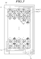
- FIG. 3 is an exemplary diagram illustrating a touch sensor structure within a touch area of the display panel according to the embodiments of the present disclosure
- FIG. 4 is another exemplary diagram of a touch panel in the display device according to the embodiments of the present disclosure.
- FIG. 5 is a diagram illustrating a non-mesh-type touch electrode in the display panel according to the embodiments of the present disclosure
- FIG. 6 is a diagram illustrating a mesh-type touch electrode in the touch panel according to the embodiments of the present disclosure
- FIG. 7 is a diagram for explaining a correspondence relationship between a mesh-type touch electrode TE and sub-pixels arranged on a touch panel TSP in the display device according to the embodiments of the present disclosure.
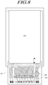
- FIG. 8 is a diagram illustrating a structure in which touch lines and data link lines are disposed in a non-display area according to a touch sensor structure of the display panel according to the embodiments of the present disclosure
- FIG. 9 is a cross-sectional view of a portion of FIG. 8
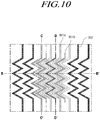
- FIG. 10 is a diagram schematically illustrating the touch lines and data link lines disposed in the bendable area of FIG. 8 according to an embodiment of the present disclosure
- FIG. 11 is a cross-sectional view of a portion of FIG. 10
- FIG. 12 is a cross-sectional view taken along line C-C' in FIG. 10
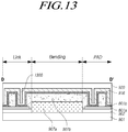
- FIG. 13 is a cross-sectional view taken along line D-D' in FIG. 10
- FIG. 14 is a diagram schematically illustrating the touch lines and data link lines disposed in the bendable area of FIG. 8 according to another embodiment of the present disclosure
- FIG. 15 is a cross-sectional view of a portion of FIG. 14
- FIG. 16 is a cross-sectional view taken along line D-D' in FIG. 14
- FIG. 17 is a diagram illustrating a structure in which touch lines are disposed in a non-display area according to a touch sensor structure of the display panel according to the embodiments of the present disclosure
- FIG. 17 is a diagram illustrating a structure in which touch lines are disposed in a non-display area according to a touch sensor structure of the display panel according to the embodiments of the present disclosure
- FIG. 18 is a diagram illustrating a portion of FIG. 17 according to an embodiment of the present disclosure
- FIG. 19 is a cross-sectional view of a portion of FIG. 18
- FIG. 20 is a diagram illustrating a portion of FIG. 17 according to another embodiment of the present disclosure
- FIG. 21 is a cross-sectional view of a portion of FIG. 20
- FIG. 22 is a diagram illustrating a partial configuration in FIG. 21 in more detail.
- FIG. 1 is a system configuration diagram of a display device according to embodiments of the present disclosure.
- a display device may provide an image display function for displaying images and a touch sensing function for sensing a user's touch.
- a display device may include: a display panel DISP in which a plurality of data lines and a plurality of gate lines are arranged for image display and a plurality of sub pixels defined by the plurality of data lines and the plurality of gate lines are arranged; a display driving circuit configured to drive the plurality of data lines and the plurality of gate lines; and the like.
- the display driving circuit may include a data driving circuit DDC configured to drive data lines, a gate driving circuit GDC configured to drive gate lines, a display controller D-CTR configured to control the data driving circuit DDC and the gate driving circuit GDC, and the like.
- the display device may include a touch panel TSP, in which a plurality of touch electrodes TE are disposed, as a touch sensor for touch sensing, and a touch sensing circuit TSC configured to perform driving and sensing processing of the touch panel TSP, and the like.
- a touch panel TSP in which a plurality of touch electrodes TE are disposed, as a touch sensor for touch sensing, and a touch sensing circuit TSC configured to perform driving and sensing processing of the touch panel TSP, and the like.
- the touch sensing circuit TSC supplies a driving signal to the touch panel TSP in order to drive the touch panel TSP, detects a sensing signal from the touch panel TSP, and senses presence or absence of a touch and/or a touch position (touch coordinates).
- Such a touch sensing circuit TSC may include a touch driving circuit TDC configured to supply a driving signal and to receive a sensing signal, a touch controller T-CTR configured to calculate presence or absence of a touch and/or a touch position (touch coordinates), and the like.
- the touch sensing circuit TSC may be implemented with one or more components (e.g., integrated circuits), and may be implemented separately from the display driving circuit.
- the entirety or a part of the touch sensing circuit TSC may be integrated with the display driving circuit and one or more of the internal circuits of the display driving circuit.
- the touch driving circuit TDC of the touch sensing circuit TSC can be implemented as an integrated circuit together with the data driving circuit DDC of the display driving circuit.
- the display device is capable of sensing a touch based on a capacitance formed on the touch electrodes TE.
- the display device adopts a capacitance-based touch sensing scheme, in which a touch may be sensed by a mutual-capacitance-based touch sensing scheme or by a self-capacitance-based touch sensing scheme.
- FIGS. 2 to 4 are three exemplary diagrams of a touch panel TSP in the display device according to the embodiments of the present disclosure, in which FIGS. 2 and 3 are exemplary diagrams of a touch panel TSP when the display device according to the embodiments of the present disclosure senses a touch by the mutual-capacitance-based touch sensing scheme and FIG. 4 is an exemplary diagram of a touch panel TSP when the display device according to the embodiments of the present disclosure senses a touch by the self-capacitance-based touch sensing scheme.
- a plurality of touch electrodes TE arranged in a touch panel TSP may be classified into a driving touch electrode (also referred to as a driving electrode, a transmission electrode, or a driving line) to which a driving signal is applied, and a sensing touch electrode (also referred to as a sensing electrode, a reception electrode, or a sensing line) from which a sensing signal is sensed and which forms a capacitance with the driving electrode.
- a driving touch electrode also referred to as a driving electrode, a transmission electrode, or a driving line
- a sensing touch electrode also referred to as a sensing electrode, a reception electrode, or a sensing line
- the driving touch electrodes arranged in the same row (or the same column) are electrically connected to each other by an integration method (or by a connection method using a bridge pattern) so as to form one driving touch electrode line DEL.
- sensing touch electrodes (Sensing TE) in the touch electrodes TE
- the sensing touch electrodes arranged in the same column (or the same row) are electrically connected to each other by a bridge pattern BP (or by an integration method) so as to form one sensing touch electrode line SEL.
- the touch sensing circuit TSC applies a driving signal to one or more driving touch electrode lines DEL and receives a sensing signal from one or more sensing touch electrode lines SEL. Based on the received sensing signal, the presence or absence and/or coordinates of a touch are detected based on a change in capacitance (mutual-capacitance) between the driving touch electrode lines DEL and the sensing touch electrode lines SEL depending on the presence or absence of a pointer such as a finger or a pen.
- each of the plurality of driving touch electrode lines DEL and each of the plurality of sensing touch electrode lines SEL are electrically connected to a touch driving circuit TDC via one or more touch lines TL.
- each of the plurality of driving touch electrode lines DEL is electrically connected to the touch driving circuit TDC via one or more driving touch lines TLd.
- each of the plurality of sensing touch electrode lines SEL is electrically connected to the touch driving circuit TDC via one or more sensing touch lines TLs.
- each touch electrode TE disposed in the touch panel TSP has both the role of a driving touch electrode (driving signal application) and the role of a sensing touch electrode (sensing signal detection).
- a driving signal is applied to each touch electrode TE, and a sensing signal is received via the touch electrode TE to which the driving signal is applied. Therefore, in the self-capacitance-based touch sensing scheme, a driving electrode and a sensing electrode are not separately distinguished from each other.
- the touch sensing circuit TSC applies a driving signal to at least one touch electrode TE, receives a sensing signal from the touch electrode TE to which a driving signal is applied, and detects the presence or absence and/or coordinates of a touch based on a change in capacitance between a pointer such as a finger or a pen and the touch electrode TE, based on the received sensing signal.
- each of the plurality of touch electrodes TE is electrically connected to the touch driving circuit TDC via one or more touch lines TL.
- the display device may sense a touch by the mutual-capacitance-based touch sensing scheme, or may sense a touch by the self-capacitance-based touch sensing scheme.
- the mutual-capacitance-based touch sensing scheme is applied to the display device and the touch panel TSP according to the embodiments of the present disclosure.
- the self-capacitance-based touch sensing scheme may also be equally applied to the display device and the touch panel TSP according to the embodiments of the present disclosure.
- the touch panel TSP may be of an externally-attached type manufactured separately from a display panel DISP and bonded to the display panel DISP, or may be of a built-in type which is manufactured together with the display panel DISP and is present inside the display panel DISP.
- the touch panel TSP is of a built-in type in which the touch panel TSP exists inside the display panel DISP.
- the touch electrodes TE and the touch lines TL are electrodes and signal lines existing inside the display panel DISP.
- the display panel DISP of the display device may be of various types such as an OLED panel and an LCD panel.
- an OLED panel will be mainly described as an example.
- FIG. 5 is a diagram illustrating a non-mesh-type touch electrode TE disposed on the touch panel TSP in the display device according to the embodiments of the present disclosure.
- each of the plurality of touch electrodes TE disposed on the touch panel TSP may be of a non-mesh type.
- the non-mesh-type touch electrode TE may be a plate-shaped metal electrode having no open area.
- the touch electrodes TE may be transparent electrodes.
- FIG. 6 is a diagram illustrating a mesh-type touch electrode disposed on a touch panel TSP in the display device according to the embodiments of the present disclosure.
- each of the plurality of touch electrodes TE disposed on the touch panel TSP may be of a mesh type.
- the mesh-type touch electrode TE may be made of an electrode metal EM patterned in a mesh type.
- a plurality of open areas OA may exist in the area of the mesh-type touch electrode TE.
- FIG. 7 is a diagram for explaining a correspondence relationship between a mesh-type touch electrode TE disposed on a touch panel TSP and sub-pixels in the display device according to the embodiments of the present disclosure.
- each of the plurality of open areas OA existing in the area of a touch electrode TE made of an electrode metal EM patterned in a mesh type, may correspond to a light-emitting region of one or more sub-pixels.
- each of the plurality of open areas OA, existing in the area of one touch electrode TE may correspond to at least one of red, green, and blue sub-pixels.
- each of the plurality of open areas OA, existing in the area of one touch electrode TE may correspond to at least one of red, green, blue, and white sub-pixels.
- the light-emitting area of one or more sub-pixels exists in each of the open areas OA of each touch electrode TE in a plan view, it is possible to further increase the opening ratio and light emission efficiency of a display panel DISP while enabling touch sensing.
- the outline of one touch electrode TE may have an approximately rhombic or rectangular shape (including a square shape), for example, and an open area OA corresponding to a hole in one touch electrode TE may also have a rhombic or rectangular shape (including a square shape), for example.
- the shape of the touch electrode TE and the shape of the open area OA may be variously modified and designed in consideration of the shape of sub-pixels, the arrangement structure of the sub-pixels, touch sensitivity, and the like.
- FIG. 8 is a diagram illustrating a structure in which touch lines and data link lines are disposed in a non-display area according to a touch sensor structure of the display panel according to the embodiments of the present disclosure.
- a plurality of data link lines 801 and a plurality of touch lines 802 are disposed on the non-display area which is an outer area of the display area A/A of the display panel DISP.
- the data link lines 801 may be formed by extending the data lines DL or may be electrically connected to the data lines DL.
- the data link lines 801 may be formed of a material, which is the same as or different from the material of the data lines DL, and may be disposed on a layer, which is the same as or different from the layer of the data lines DL.
- the touch lines 802 are electrically connected to the touch electrodes TE and may be formed of the same material as an electrode metal EM that forms the touch electrode TE.
- a data pad is provided at the end of each data link line 801 to be electrically connected to the data driving circuit DDC.
- a touch pad is provided at an end of each touch line 802 to be electrically connected to the touch driver circuit TDC.
- the plurality of data link lines 801 and the plurality of touch lines 802, disposed on the non-display area may be disposed in a first bendable area BA which may be the entire non-display area or a portion of the non-display area.
- the first bendable area BA may become a bent area by bending a portion of the substrate of the display panel DISP.
- the data link lines 801 and the touch lines 802 themselves are bent, electrical connection to the data driving circuit DDC or the touch driving circuit TDC can be more easily performed.
- FIG. 9 is a cross-sectional view of a portion of FIG. 8 .
- FIG. 9 is a cross-sectional view taken along line A-A in FIG. 8 .
- the cross-sectional structure of the display panel DISP will be described with reference to FIG. 9 .
- a polyimide layer 901 is placed on a substrate or a back plate.
- the polyimide layer 901 may be placed on the substrate or may be present without the substrate.
- the substrate may be present without the polyimide layer 901. That is, in this case, the substrate may be regarded as the polyimide layer 901.
- the substrate may be flexible or non-flexible.
- first buffer layer 902 and the second buffer layer 903 are placed and a gate insulating film 904 and a multilayered insulating film 905 are placed on the second buffer layer 903.
- a source/drain layer is present on an inorganic film layer.
- various signal lines such as data lines DL and source/drain electrodes 906 of various transistors are formed in a display area A/A.
- the data link line 801 or the like may be formed in a non-display area in the same layer as the source/drain layer.
- a planarization layer 907 made of an organic material is placed on the source/drain layer.
- a first electrode 908 is located at the light-emitting position of each sub-pixel, and a bank 910 is placed on the first electrode 908.
- the first electrode 908 since the first electrode 908 is present in each sub-pixel, the first electrode 908 may be called a pixel electrode.
- an organic light-emitting layer 911 is placed on the first electrode 911 between two adjacent banks 910.
- a second electrode 909 is placed on the organic light-emitting layer 911.
- the second electrode 909 may be a common electrode formed in common to all sub-pixel areas.
- an encapsulation layer for preventing penetration of moisture, air, and the like may be present.
- the encapsulation layer may be laminated in a single layer or in two or more layers. Further, the encapsulation layer may be formed of a metallic layer, or may be formed by laminating organic and inorganic layers in two or more layers.
- FIG. 9 illustrates a case in which the encapsulation layer 914 is formed by laminating a first encapsulation layer 912, a second encapsulation layer 913, and a third encapsulation layer 914.
- the first encapsulation layer 912 may be a first inorganic film
- the second encapsulation layer 913 may be an organic film
- the third encapsulation layer 913 may be a second inorganic film.
- a touch buffer layer 915 is placed on the encapsulation layer or the third sealing layer 913 and the touch insulating film 916 is placed on the touch buffer layer 915.
- touch electrodes 917 are formed on the touch insulating film 916.
- the touch electrodes 917 illustrated in FIG. 9 may be driving touch electrodes TEd or sensing touch electrodes TEs.
- bridge patterns 918 may be formed between the touch buffer layer 915 and the touch insulating film 916.
- the bridge patterns 918 connect two or more sensing touch electrodes TEs, and when the touch electrodes 917 are the sensing touch electrodes TEs, the bridge patterns 918 connect two or more driving touch electrodes TEd.
- the touch electrodes 917 and the bridge patterns 918 are made of an electrode metal EM.
- the touch electrodes 917 and the bridge patterns 918 may be patterned as a mesh having a plurality of open areas therein, at least some of the open areas corresponding to a light-emitting area of at least one sub-pixel.
- a protective film 920 is placed on the touch insulating film 916 and the touch electrodes 917.
- the protective film 920 may extend from the display area A/A to the non-display area.
- FIG. 10 is a diagram schematically illustrating the touch lines and data link lines disposed in the first bendable area of FIG. 8 according to an embodiment of the present disclosure.
- the plurality of data link lines 801 and the plurality of touch lines 802 are disposed in the first bendable area BA of FIG. 8 .
- FIG. 10 only illustrates some of the data link lines 801 and the touch lines 802 of FIG. 10 schematically.
- the plurality of data link lines 801 and the plurality of touch lines 802 disposed on the first bendable area BA may be disposed on the same plane while forming a zigzag pattern.
- the damage of the data link lines 801 and the touch lines 802 may be minimized, despite an external force applied due to the curvature of the first bendable area BA when the first bendable area BA is bent.
- FIG. 11 is a cross-sectional view of a portion of FIG. 10 . Specifically, FIG. 11 is a cross-sectional view taken along line B-B' in FIG. 10 .
- FIG. 11 a structure, in which a polyimide layer 901, a first planarization layer 907a, a second planarization layer 907b, a touch insulating film 916, and a protection film 920 are laminated, is illustrated in the cross section of the first bendable area BA of FIG. 8 .
- the plurality of data link lines 801 are disposed on the first planarization layer 907a in the first bendable area BA.
- the plurality of data link lines 801 may be made of a source/drain metal.
- inter-line short-circuit may occur as the number of lines increase.
- the plurality of data link lines 801 may be alternately disposed in two or more layers in the first bendable area BA.
- the plurality of data link lines 801 are disposed on the first planarization layer 907a, and the remaining data link lines 801 are disposed on the second planarization layer 907b.
- the plurality of data link lines 801 are disposed in two or more layers.
- the plurality of data link lines 801 disposed in two or more layers may be alternately disposed, which is for a structure in which the plurality of data link lines 801 disposed on the same layer are disposed in the first bendable area BA in such a manner that some of the plurality of data link lines 801 are located to jump to another layer and the remaining data link lines 801 are located on the existing layer.
- the plurality of data link lines 801 on the first planarization layer 907a may not align with the plurality of data link lines 801 on the second planarization layer 907b.
- first data link lines 801a the line disposed on a first one of the two or more layers may be defined as first data link lines 801a
- second data link lines 801b the line disposed on a second layer of two or more layers.
- the second data link lines 801b are disposed on an upper layer and the first data link lines 801a are disposed on a lower layer.
- the upper layer is a layer further away from the polyamide layer 901 than the lower layer.
- the second data link lines 801b may be disposed on the second planarization layer 907b
- the first data link lines 801a may be disposed on the first planarization layer 907a.
- the plurality of touch lines 802 are disposed on the second planarization layer 907b of the first bendable area BA.
- the plurality of touch lines 802 may be formed of an electrode metal EM.
- the plurality of touch lines 802 may include touch lines 802b, which are connected to the touch electrodes 917, and touch lines 802a, which are connected to a bridge pattern 918, in which the touch lines 802b and the touch lines 802a are dually disposed in different layers.
- the touch lines 802b connected to the touch electrodes 917 may be disposed in a layer higher than the touch lines 802a connected to the bridge pattern 918.
- the touch lines 802b connected to the touch electrodes 917 may be disposed on the touch insulating film 916 and the touch lines 802a connected to the bridge pattern 918 may be disposed on the second planarization layer 907b.
- the data link lines 801 disposed on one of the two or more layers may be made of the same metal as at least one touch line 802 among the plurality of touch lines 802.
- the metal may be an electrode metal EM.
- the bridge patterns 918 or the plurality of touch electrodes 917 may be arranged to overlap the bank 910 of at least one sub-pixel.
- the second data link lines 801b may be connected to at least one of the plurality of touch lines 802 and may be made of the same metal as the touch lines 802.
- the second data link lines 801b disposed on the upper layer may be formed of the same metal as the at least one touch line 802 among the plurality of touch lines 802.
- the metal constituting the first data link lines 801a and the metal constituting the second data link lines 801b may be different from each other.
- the second data link lines 801b may be disposed on the same layer as the touch lines 802a and may be made of the electrode metal EM that constitutes the touch lines 802a. Since the second data link lines 801b and the touch lines 802a may be simultaneously manufactured in the same process, it is not necessary to perform a separate process for applying the alternate structure.
- first data link lines 801a are disposed on the first planarization layer 907a and are made of a source/drain metal
- second data link lines 802b are disposed on the second planarization layer 907b and are made of an electrode metal EM.
- FIG. 12 is a cross-sectional view taken along line C-C' in FIG. 10
- FIG. 13 is a cross-sectional view taken along line D-D' in FIG. 10 .
- the first data link line 801a is continuously disposed from a link area of the outer non-display area of the display panel DISP to a pad area.
- the first data link line 801a extends from the link area of the outer non-display area of the display panel DISP to the first bendable area BA and is broken in the first bendable area BA.
- the first data link line 801a is electrically connected to the second data link line 801b, which is located at the upper layer, via at least one via hole 1300.
- the first data link line 801a in the cross section along line C-C' in FIG. 10 is disposed on the first planarization layer 907a in the first bendable area BA so as to transmit a signal, and the first data link line 801a in the cross section along line D-D' in FIG. 10 jumps onto the second planarization layer 907b in the first bendable area BA and transmits a signal to the second data link line 801b disposed on the second planarization layer 907b.
- the second data link line 801b disposed on the second planarization layer 907b in the cross section along line D-D' in FIG. 10 , is again electrically connected to the first data link line 801a, disposed on the first planarization layer 907a, via a via hole 1300 which passes through the second planarization layer 907b.
- the data link lines 801 are alternately placed in different layers only in the first bendable area BA where the space restriction is more severe, and in the areas other than the first bendable area BA, the data link lines 801 are placed on the same layer, thereby making it possible to have an efficient line structure without applying the alternate structure to the entire non-display area.
- the touch buffer layer 915 may also be located in the PAD area between the second planarization layer 907b and the touch insulating film 916.
- the second data link line 801b is electrically connected to the first data link line 801a via the via hole 1300.
- the second data link line 801b is formed on the touch buffer layer 915. Therefore, the via hole 1300 passes through both the second planarization layer 907b and the touch buffer layer 915 to allow electrical contact of the second data link line 801b and the first data link line 801a.
- the touch insulating film 916 As the touch insulating film 916 is disposed on the second data link line 801b, the touch insulating film 916 defines the via hole 1300 as shown in FIG. 13 .
- the plurality of touch lines 802, disposed on the touch insulating film 916 may extend to the pad area.
- Such touch lines may connect to the first data link line 801a in the pad area via a touch contact hole such that the touch lines are electrically connected to the first data link line 801a.
- the touch contact hole may therefore pass through the touch insulating film 916, the second planarization layer 907b and the touch buffer layer 915.
- the touch sensor 917 is connected to the touch driving circuit via the electrical connection of the touch lines to the first data link line 801a.
- Touch line connects to first data link line 801a via a via hole in the pad area.
- First data link line 801a electrically connects to touch line.
- FIG. 14 is a diagram schematically illustrating the touch lines and data link lines disposed in the first bendable area of FIG. 8 according to another embodiment of the present disclosure. Descriptions of components, which are the same or similar to those of FIGS. 10 to 13 , will be omitted in the following description.
- the plurality of data link lines 801 and the plurality of touch lines 802 are disposed in the first bendable area BA of FIG. 8 .
- some of the plurality of data link lines 801 in FIG. 14 are configured as dual lines in two or more layers again.
- FIG. 15 is a cross-sectional view taken along line B-B' in FIG. 14 . More specifically, referring to FIG. 15 , the plurality of data link lines 801 may further include, in addition to the first data link lines 801a and the second data link lines 801b, a plurality of third data link lines 801c provided on the layer above the second data link lines 801b so as to overlap the second data link lines 801b.
- the third data link lines 801c are located on the touch insulating film 916 so as to be located on a layer above the first data link lines 801a and the second data link lines 801b.
- the third data link lines 801c may be located on the same layer as the touch lines 802b located on the touch insulating film 916 and may be made of the same metal as the touch lines 802b. In this case, the third data link lines 801c is made of an electrode metal EM.
- FIG. 16 is a cross-sectional view taken along line D-D' in FIG. 14 .
- the third data link line 801c is located on the touch insulating film 916 which is a layer above the second data link line 801b.
- the third data link line 801c is electrically connected to the second data line 801b through at least one via hole 1600 and is also electrically connected to the first data line 801a through the second data line 801b.
- the resistance of the lines can be lowered, thereby enabling effective signal transmission.
- FIG. 17 is a diagram illustrating a structure in which touch lines are disposed in a non-display area according to a touch sensor structure of the display panel according to the embodiments of the present disclosure.
- the plurality of touch lines 802 are disposed in the non-display area of the display panel DISP, particularly, in a bezel area.
- the bottom surface of the display panel DISP is only made of the polyimide layer 901 or the substrate is flexible, at least a portion of the display area A/A of the display panel DISP can be folded.
- some of the plurality of touch lines 802 pass the second bendable areas FA of the display panel DISP.
- FIG. 18 is a diagram illustrating a portion of FIG. 17 according to an embodiment of the present disclosure
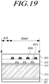
- FIG. 19 is a cross-sectional view of a portion of FIG. 18 .
- the plurality of touch lines 802, passing through the second bendable area FA of the display panel DISP, may be disposed on the same plane while forming a zigzag pattern.
- the damage of the touch lines 802 can be minimized, despite the external force applied due to the curvature of the second bendable area FA when the second bendable area FA is bent.
- the plurality of touch lines 802, passing through the second bendable area FA may be alternately disposed in two or more layers.
- the touch lines 802a are disposed on one of two or more layers, and the touch lines 802b are disposed on another one of the two or more layers.
- the touch lines 802a and 802b may be lines electrically connected to the touch electrodes 917 and the bridge pattern 918 as described above.
- touch lines 802a and 802b are formed in this alternate structure, as compared with a case where the touch lines 802a and 802b are disposed on different layers to overlap the same line as dual lines, it is possible to form respective touch lines 802a and 802b to be closer to each other, thereby implementing a narrow bezel.
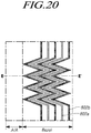
- FIG. 20 is a diagram illustrating a portion of FIG. 17 according to another embodiment of the present disclosure
- FIG. 21 is a cross-sectional view of a portion of FIG. 20
- FIG. 22 is a diagram illustrating a partial configuration in FIG. 21 in more detail.
- the touch line 802b closest to the display area A/A of the display panel DISP is in contact with the boundary of the display area A/A, unlike the case illustrated in FIG. 18 .
- the touch lines 802a and 802b are alternately disposed, so that the touch lines 802b adjacent to the display area A/A located in the upper layer are capable of being shifted in the same bezel size, and thus it is possible to secure a wider area per one line.
- the display panel DISP is capable of having a structure more resistant to an external force applied due to the folding of the second bendable area FA, thereby preventing the touch lines 802a and 802b from being cracked.
- the zigzag angle of the touch lines 802a and 802b may be variable to a point where the bent portion of the touch line 802b closest to the display area A/A of the display panel DISP meets the boundary of the display area A/A.
- the bent angle ⁇ of the zigzag pattern may be variable to a range where the bent portions of the touch lines 802b meet the display area A/A of the display panel DISP.
Landscapes
- Engineering & Computer Science (AREA)
- Theoretical Computer Science (AREA)
- General Engineering & Computer Science (AREA)
- Human Computer Interaction (AREA)
- Physics & Mathematics (AREA)
- General Physics & Mathematics (AREA)
- Computer Hardware Design (AREA)
- Computer Networks & Wireless Communication (AREA)
- Microelectronics & Electronic Packaging (AREA)
- Devices For Indicating Variable Information By Combining Individual Elements (AREA)
- Electroluminescent Light Sources (AREA)
- Position Input By Displaying (AREA)
Applications Claiming Priority (1)
| Application Number | Priority Date | Filing Date | Title |
|---|---|---|---|
| KR1020170141558A KR102588343B1 (ko) | 2017-10-27 | 2017-10-27 | 터치 디스플레이 장치 |
Publications (3)
| Publication Number | Publication Date |
|---|---|
| EP3477442A2 true EP3477442A2 (de) | 2019-05-01 |
| EP3477442A3 EP3477442A3 (de) | 2019-06-26 |
| EP3477442B1 EP3477442B1 (de) | 2021-09-29 |
Family
ID=63762351
Family Applications (1)
| Application Number | Title | Priority Date | Filing Date |
|---|---|---|---|
| EP18198574.8A Active EP3477442B1 (de) | 2017-10-27 | 2018-10-04 | Anzeigevorrichtung |
Country Status (5)
| Country | Link |
|---|---|
| US (3) | US10768742B2 (de) |
| EP (1) | EP3477442B1 (de) |
| KR (1) | KR102588343B1 (de) |
| CN (2) | CN114625286B (de) |
| TW (1) | TWI683246B (de) |
Cited By (2)
| Publication number | Priority date | Publication date | Assignee | Title |
|---|---|---|---|---|
| CN112151577A (zh) * | 2019-06-28 | 2020-12-29 | 乐金显示有限公司 | 显示装置 |
| EP4033554A4 (de) * | 2019-09-17 | 2023-09-27 | Jrd Communication (Shenzhen) Ltd. | Berührungsbildschirm und mobiles endgerät |
Families Citing this family (18)
| Publication number | Priority date | Publication date | Assignee | Title |
|---|---|---|---|---|
| KR102380755B1 (ko) * | 2017-10-25 | 2022-03-30 | 엘지디스플레이 주식회사 | 터치 디스플레이 패널 및 터치 디스플레이 장치 |
| US11404525B2 (en) * | 2018-03-01 | 2022-08-02 | Sharp Kabushiki Kaisha | Display device and method for manufacturing display device |
| JP6946220B2 (ja) * | 2018-03-26 | 2021-10-06 | 株式会社ジャパンディスプレイ | 表示装置 |
| KR102640726B1 (ko) * | 2018-04-18 | 2024-02-27 | 삼성디스플레이 주식회사 | 유기 발광 표시 장치 |
| KR102883834B1 (ko) * | 2019-01-30 | 2025-11-10 | 삼성디스플레이 주식회사 | 디스플레이 장치 |
| CN110164933B (zh) * | 2019-05-24 | 2021-05-18 | 苏州清越光电科技股份有限公司 | 显示面板及显示装置 |
| KR102810071B1 (ko) | 2019-08-19 | 2025-05-21 | 엘지디스플레이 주식회사 | 터치 디스플레이 장치 |
| KR102774908B1 (ko) | 2020-05-27 | 2025-03-05 | 삼성디스플레이 주식회사 | 전자 장치 |
| CN112433632B (zh) * | 2020-11-19 | 2022-06-21 | 湖北长江新型显示产业创新中心有限公司 | 一种显示面板及其制备方法、显示装置 |
| KR20220097671A (ko) | 2020-12-30 | 2022-07-08 | 삼성디스플레이 주식회사 | 디스플레이 패널 |
| CN115315810B (zh) * | 2021-03-04 | 2025-04-01 | 京东方科技集团股份有限公司 | 显示面板及其制造方法、显示装置 |
| KR20230026595A (ko) | 2021-08-17 | 2023-02-27 | 삼성디스플레이 주식회사 | 표시 장치 |
| CN113782559B (zh) * | 2021-09-14 | 2023-11-07 | 业成科技(成都)有限公司 | 导电模组及显示装置 |
| CN115808984A (zh) * | 2021-09-14 | 2023-03-17 | 京东方科技集团股份有限公司 | 显示基板及显示装置 |
| KR102909822B1 (ko) * | 2021-12-24 | 2026-01-07 | 엘지디스플레이 주식회사 | 커브드 디스플레이 장치 |
| KR20230103605A (ko) * | 2021-12-31 | 2023-07-07 | 엘지디스플레이 주식회사 | 디스플레이 장치 |
| EP4517414A4 (de) | 2022-05-26 | 2025-07-02 | Boe Technology Group Co Ltd | Berührungsanzeigetafel und anzeigevorrichtung |
| KR20250001298A (ko) * | 2023-06-28 | 2025-01-06 | 엘지디스플레이 주식회사 | 표시 장치 및 표시 패널 |
Citations (1)
| Publication number | Priority date | Publication date | Assignee | Title |
|---|---|---|---|---|
| EP3217265A1 (de) * | 2016-03-11 | 2017-09-13 | Samsung Display Co., Ltd. | Anzeigevorrichtung und verfahren zur herstellung davon |
Family Cites Families (14)
| Publication number | Priority date | Publication date | Assignee | Title |
|---|---|---|---|---|
| KR101520423B1 (ko) * | 2011-04-21 | 2015-05-14 | 엘지디스플레이 주식회사 | 터치센서 인셀 타입 액정표시장치용 어레이 기판 및 이의 제조방법 |
| US9195108B2 (en) * | 2012-08-21 | 2015-11-24 | Apple Inc. | Displays with bent signal lines |
| KR102058699B1 (ko) * | 2013-01-24 | 2019-12-26 | 삼성디스플레이 주식회사 | 터치 및 휨 감지 기능을 가지는 플렉서블 표시장치 |
| US9276055B1 (en) * | 2014-08-31 | 2016-03-01 | Lg Display Co., Ltd. | Display device with micro cover layer and manufacturing method for the same |
| US9356087B1 (en) * | 2014-12-10 | 2016-05-31 | Lg Display Co., Ltd. | Flexible display device with bridged wire traces |
| KR101678590B1 (ko) * | 2014-12-26 | 2016-11-23 | 엘지디스플레이 주식회사 | 액정표시패널 및 이를 이용한 액정표시장치 |
| US10168844B2 (en) * | 2015-06-26 | 2019-01-01 | Samsung Display Co., Ltd. | Flexible display device |
| KR102394723B1 (ko) * | 2015-09-30 | 2022-05-09 | 엘지디스플레이 주식회사 | 터치 스크린 패널 및 이를 포함하는 표시 장치 |
| US10361385B2 (en) * | 2016-02-12 | 2019-07-23 | Samsung Display Co., Ltd. | Display device |
| KR102505879B1 (ko) * | 2016-03-24 | 2023-03-06 | 삼성디스플레이 주식회사 | 디스플레이 장치 |
| KR102451726B1 (ko) * | 2016-03-28 | 2022-10-07 | 삼성디스플레이 주식회사 | 표시 장치 및 이의 제조 방법 |
| KR102601207B1 (ko) * | 2016-07-29 | 2023-11-13 | 삼성디스플레이 주식회사 | 표시장치 |
| CN106898635B (zh) * | 2017-02-28 | 2020-04-07 | 上海天马微电子有限公司 | 显示面板、显示装置 |
| CN106959783B (zh) * | 2017-04-05 | 2020-06-26 | 上海中航光电子有限公司 | 阵列基板、触控面板和触控装置 |
-
2017
- 2017-10-27 KR KR1020170141558A patent/KR102588343B1/ko active Active
-
2018
- 2018-10-04 EP EP18198574.8A patent/EP3477442B1/de active Active
- 2018-10-15 TW TW107136215A patent/TWI683246B/zh active
- 2018-10-24 US US16/169,927 patent/US10768742B2/en active Active
- 2018-10-25 CN CN202210300497.3A patent/CN114625286B/zh active Active
- 2018-10-25 CN CN201811249306.5A patent/CN109725757B/zh active Active
-
2020
- 2020-07-31 US US16/944,721 patent/US11237592B2/en active Active
-
2021
- 2021-12-21 US US17/558,082 patent/US11460883B2/en active Active
Patent Citations (1)
| Publication number | Priority date | Publication date | Assignee | Title |
|---|---|---|---|---|
| EP3217265A1 (de) * | 2016-03-11 | 2017-09-13 | Samsung Display Co., Ltd. | Anzeigevorrichtung und verfahren zur herstellung davon |
Cited By (5)
| Publication number | Priority date | Publication date | Assignee | Title |
|---|---|---|---|---|
| CN112151577A (zh) * | 2019-06-28 | 2020-12-29 | 乐金显示有限公司 | 显示装置 |
| EP3757734A1 (de) * | 2019-06-28 | 2020-12-30 | LG Display Co., Ltd. | Berührungsempfindliche anzeigevorrichtung mit reduziertem randbereich |
| US11195888B2 (en) | 2019-06-28 | 2021-12-07 | Lg Display Co., Ltd. | Display device |
| CN112151577B (zh) * | 2019-06-28 | 2025-09-19 | 乐金显示有限公司 | 显示装置 |
| EP4033554A4 (de) * | 2019-09-17 | 2023-09-27 | Jrd Communication (Shenzhen) Ltd. | Berührungsbildschirm und mobiles endgerät |
Also Published As
| Publication number | Publication date |
|---|---|
| US11237592B2 (en) | 2022-02-01 |
| US10768742B2 (en) | 2020-09-08 |
| TW201923530A (zh) | 2019-06-16 |
| CN109725757B (zh) | 2022-04-12 |
| US20220113760A1 (en) | 2022-04-14 |
| EP3477442A3 (de) | 2019-06-26 |
| CN114625286A (zh) | 2022-06-14 |
| US20200363899A1 (en) | 2020-11-19 |
| CN114625286B (zh) | 2025-04-15 |
| CN109725757A (zh) | 2019-05-07 |
| US11460883B2 (en) | 2022-10-04 |
| KR20190047549A (ko) | 2019-05-08 |
| US20190129567A1 (en) | 2019-05-02 |
| EP3477442B1 (de) | 2021-09-29 |
| KR102588343B1 (ko) | 2023-10-11 |
| TWI683246B (zh) | 2020-01-21 |
Similar Documents
| Publication | Publication Date | Title |
|---|---|---|
| US11460883B2 (en) | Display device | |
| KR102500568B1 (ko) | 터치표시장치 및 표시패널 | |
| KR102861579B1 (ko) | 터치스크린 내장형 유기발광표시패널 및 유기발광표시장치 | |
| US11275459B2 (en) | Touch display device and touch display panel having a curved active area and improving a touch sensitivity at a curved portion | |
| US11157102B2 (en) | Touch display device and panel | |
| US11550193B2 (en) | Display device | |
| KR102526215B1 (ko) | 터치패널 및 이를 포함하는 터치표시장치 | |
| US10976871B2 (en) | Touch display device and panel including mesh type electrodes | |
| JP6375361B2 (ja) | タッチスクリーン内蔵型有機発光表示パネル及び有機発光表示装置 | |
| US11199930B2 (en) | Touch display device and method for manufacturing touch display device |
Legal Events
| Date | Code | Title | Description |
|---|---|---|---|
| PUAI | Public reference made under article 153(3) epc to a published international application that has entered the european phase |
Free format text: ORIGINAL CODE: 0009012 |
|
| STAA | Information on the status of an ep patent application or granted ep patent |
Free format text: STATUS: REQUEST FOR EXAMINATION WAS MADE |
|
| 17P | Request for examination filed |
Effective date: 20181004 |
|
| AK | Designated contracting states |
Kind code of ref document: A2 Designated state(s): AL AT BE BG CH CY CZ DE DK EE ES FI FR GB GR HR HU IE IS IT LI LT LU LV MC MK MT NL NO PL PT RO RS SE SI SK SM TR |
|
| AX | Request for extension of the european patent |
Extension state: BA ME |
|
| PUAL | Search report despatched |
Free format text: ORIGINAL CODE: 0009013 |
|
| AK | Designated contracting states |
Kind code of ref document: A3 Designated state(s): AL AT BE BG CH CY CZ DE DK EE ES FI FR GB GR HR HU IE IS IT LI LT LU LV MC MK MT NL NO PL PT RO RS SE SI SK SM TR |
|
| AX | Request for extension of the european patent |
Extension state: BA ME |
|
| RIC1 | Information provided on ipc code assigned before grant |
Ipc: G06F 3/041 20060101AFI20190520BHEP Ipc: H01L 51/00 20060101ALI20190520BHEP Ipc: G06F 1/16 20060101ALI20190520BHEP |
|
| RBV | Designated contracting states (corrected) |
Designated state(s): AL AT BE BG CH CY CZ DE DK EE ES FI FR GB GR HR HU IE IS IT LI LT LU LV MC MK MT NL NO PL PT RO RS SE SI SK SM TR |
|
| STAA | Information on the status of an ep patent application or granted ep patent |
Free format text: STATUS: EXAMINATION IS IN PROGRESS |
|
| 17Q | First examination report despatched |
Effective date: 20200507 |
|
| GRAP | Despatch of communication of intention to grant a patent |
Free format text: ORIGINAL CODE: EPIDOSNIGR1 |
|
| STAA | Information on the status of an ep patent application or granted ep patent |
Free format text: STATUS: GRANT OF PATENT IS INTENDED |
|
| INTG | Intention to grant announced |
Effective date: 20210416 |
|
| GRAS | Grant fee paid |
Free format text: ORIGINAL CODE: EPIDOSNIGR3 |
|
| GRAA | (expected) grant |
Free format text: ORIGINAL CODE: 0009210 |
|
| STAA | Information on the status of an ep patent application or granted ep patent |
Free format text: STATUS: THE PATENT HAS BEEN GRANTED |
|
| AK | Designated contracting states |
Kind code of ref document: B1 Designated state(s): AL AT BE BG CH CY CZ DE DK EE ES FI FR GB GR HR HU IE IS IT LI LT LU LV MC MK MT NL NO PL PT RO RS SE SI SK SM TR |
|
| REG | Reference to a national code |
Ref country code: GB Ref legal event code: FG4D |
|
| REG | Reference to a national code |
Ref country code: DE Ref legal event code: R096 Ref document number: 602018024186 Country of ref document: DE |
|
| REG | Reference to a national code |
Ref country code: CH Ref legal event code: EP Ref country code: AT Ref legal event code: REF Ref document number: 1434789 Country of ref document: AT Kind code of ref document: T Effective date: 20211015 |
|
| REG | Reference to a national code |
Ref country code: IE Ref legal event code: FG4D |
|
| REG | Reference to a national code |
Ref country code: LT Ref legal event code: MG9D |
|
| PG25 | Lapsed in a contracting state [announced via postgrant information from national office to epo] |
Ref country code: SE Free format text: LAPSE BECAUSE OF FAILURE TO SUBMIT A TRANSLATION OF THE DESCRIPTION OR TO PAY THE FEE WITHIN THE PRESCRIBED TIME-LIMIT Effective date: 20210929 Ref country code: RS Free format text: LAPSE BECAUSE OF FAILURE TO SUBMIT A TRANSLATION OF THE DESCRIPTION OR TO PAY THE FEE WITHIN THE PRESCRIBED TIME-LIMIT Effective date: 20210929 Ref country code: HR Free format text: LAPSE BECAUSE OF FAILURE TO SUBMIT A TRANSLATION OF THE DESCRIPTION OR TO PAY THE FEE WITHIN THE PRESCRIBED TIME-LIMIT Effective date: 20210929 Ref country code: FI Free format text: LAPSE BECAUSE OF FAILURE TO SUBMIT A TRANSLATION OF THE DESCRIPTION OR TO PAY THE FEE WITHIN THE PRESCRIBED TIME-LIMIT Effective date: 20210929 Ref country code: LT Free format text: LAPSE BECAUSE OF FAILURE TO SUBMIT A TRANSLATION OF THE DESCRIPTION OR TO PAY THE FEE WITHIN THE PRESCRIBED TIME-LIMIT Effective date: 20210929 Ref country code: BG Free format text: LAPSE BECAUSE OF FAILURE TO SUBMIT A TRANSLATION OF THE DESCRIPTION OR TO PAY THE FEE WITHIN THE PRESCRIBED TIME-LIMIT Effective date: 20211229 Ref country code: NO Free format text: LAPSE BECAUSE OF FAILURE TO SUBMIT A TRANSLATION OF THE DESCRIPTION OR TO PAY THE FEE WITHIN THE PRESCRIBED TIME-LIMIT Effective date: 20211229 |
|
| REG | Reference to a national code |
Ref country code: NL Ref legal event code: MP Effective date: 20210929 |
|
| REG | Reference to a national code |
Ref country code: AT Ref legal event code: MK05 Ref document number: 1434789 Country of ref document: AT Kind code of ref document: T Effective date: 20210929 |
|
| PG25 | Lapsed in a contracting state [announced via postgrant information from national office to epo] |
Ref country code: LV Free format text: LAPSE BECAUSE OF FAILURE TO SUBMIT A TRANSLATION OF THE DESCRIPTION OR TO PAY THE FEE WITHIN THE PRESCRIBED TIME-LIMIT Effective date: 20210929 Ref country code: GR Free format text: LAPSE BECAUSE OF FAILURE TO SUBMIT A TRANSLATION OF THE DESCRIPTION OR TO PAY THE FEE WITHIN THE PRESCRIBED TIME-LIMIT Effective date: 20211230 |
|
| PG25 | Lapsed in a contracting state [announced via postgrant information from national office to epo] |
Ref country code: AT Free format text: LAPSE BECAUSE OF FAILURE TO SUBMIT A TRANSLATION OF THE DESCRIPTION OR TO PAY THE FEE WITHIN THE PRESCRIBED TIME-LIMIT Effective date: 20210929 |
|
| REG | Reference to a national code |
Ref country code: CH Ref legal event code: PL |
|
| PG25 | Lapsed in a contracting state [announced via postgrant information from national office to epo] |
Ref country code: IS Free format text: LAPSE BECAUSE OF FAILURE TO SUBMIT A TRANSLATION OF THE DESCRIPTION OR TO PAY THE FEE WITHIN THE PRESCRIBED TIME-LIMIT Effective date: 20220129 Ref country code: SK Free format text: LAPSE BECAUSE OF FAILURE TO SUBMIT A TRANSLATION OF THE DESCRIPTION OR TO PAY THE FEE WITHIN THE PRESCRIBED TIME-LIMIT Effective date: 20210929 Ref country code: RO Free format text: LAPSE BECAUSE OF FAILURE TO SUBMIT A TRANSLATION OF THE DESCRIPTION OR TO PAY THE FEE WITHIN THE PRESCRIBED TIME-LIMIT Effective date: 20210929 Ref country code: PT Free format text: LAPSE BECAUSE OF FAILURE TO SUBMIT A TRANSLATION OF THE DESCRIPTION OR TO PAY THE FEE WITHIN THE PRESCRIBED TIME-LIMIT Effective date: 20220131 Ref country code: PL Free format text: LAPSE BECAUSE OF FAILURE TO SUBMIT A TRANSLATION OF THE DESCRIPTION OR TO PAY THE FEE WITHIN THE PRESCRIBED TIME-LIMIT Effective date: 20210929 Ref country code: NL Free format text: LAPSE BECAUSE OF FAILURE TO SUBMIT A TRANSLATION OF THE DESCRIPTION OR TO PAY THE FEE WITHIN THE PRESCRIBED TIME-LIMIT Effective date: 20210929 Ref country code: ES Free format text: LAPSE BECAUSE OF FAILURE TO SUBMIT A TRANSLATION OF THE DESCRIPTION OR TO PAY THE FEE WITHIN THE PRESCRIBED TIME-LIMIT Effective date: 20210929 Ref country code: EE Free format text: LAPSE BECAUSE OF FAILURE TO SUBMIT A TRANSLATION OF THE DESCRIPTION OR TO PAY THE FEE WITHIN THE PRESCRIBED TIME-LIMIT Effective date: 20210929 Ref country code: CZ Free format text: LAPSE BECAUSE OF FAILURE TO SUBMIT A TRANSLATION OF THE DESCRIPTION OR TO PAY THE FEE WITHIN THE PRESCRIBED TIME-LIMIT Effective date: 20210929 Ref country code: AL Free format text: LAPSE BECAUSE OF FAILURE TO SUBMIT A TRANSLATION OF THE DESCRIPTION OR TO PAY THE FEE WITHIN THE PRESCRIBED TIME-LIMIT Effective date: 20210929 |
|
| REG | Reference to a national code |
Ref country code: BE Ref legal event code: MM Effective date: 20211031 |
|
| PG25 | Lapsed in a contracting state [announced via postgrant information from national office to epo] |
Ref country code: MC Free format text: LAPSE BECAUSE OF FAILURE TO SUBMIT A TRANSLATION OF THE DESCRIPTION OR TO PAY THE FEE WITHIN THE PRESCRIBED TIME-LIMIT Effective date: 20210929 |
|
| REG | Reference to a national code |
Ref country code: DE Ref legal event code: R097 Ref document number: 602018024186 Country of ref document: DE |
|
| PG25 | Lapsed in a contracting state [announced via postgrant information from national office to epo] |
Ref country code: LU Free format text: LAPSE BECAUSE OF NON-PAYMENT OF DUE FEES Effective date: 20211004 Ref country code: DK Free format text: LAPSE BECAUSE OF FAILURE TO SUBMIT A TRANSLATION OF THE DESCRIPTION OR TO PAY THE FEE WITHIN THE PRESCRIBED TIME-LIMIT Effective date: 20210929 Ref country code: BE Free format text: LAPSE BECAUSE OF NON-PAYMENT OF DUE FEES Effective date: 20211031 |
|
| PLBE | No opposition filed within time limit |
Free format text: ORIGINAL CODE: 0009261 |
|
| STAA | Information on the status of an ep patent application or granted ep patent |
Free format text: STATUS: NO OPPOSITION FILED WITHIN TIME LIMIT |
|
| PG25 | Lapsed in a contracting state [announced via postgrant information from national office to epo] |
Ref country code: LI Free format text: LAPSE BECAUSE OF NON-PAYMENT OF DUE FEES Effective date: 20211031 Ref country code: CH Free format text: LAPSE BECAUSE OF NON-PAYMENT OF DUE FEES Effective date: 20211031 |
|
| 26N | No opposition filed |
Effective date: 20220630 |
|
| PG25 | Lapsed in a contracting state [announced via postgrant information from national office to epo] |
Ref country code: IE Free format text: LAPSE BECAUSE OF NON-PAYMENT OF DUE FEES Effective date: 20211004 |
|
| PG25 | Lapsed in a contracting state [announced via postgrant information from national office to epo] |
Ref country code: SI Free format text: LAPSE BECAUSE OF FAILURE TO SUBMIT A TRANSLATION OF THE DESCRIPTION OR TO PAY THE FEE WITHIN THE PRESCRIBED TIME-LIMIT Effective date: 20210929 |
|
| PG25 | Lapsed in a contracting state [announced via postgrant information from national office to epo] |
Ref country code: IT Free format text: LAPSE BECAUSE OF FAILURE TO SUBMIT A TRANSLATION OF THE DESCRIPTION OR TO PAY THE FEE WITHIN THE PRESCRIBED TIME-LIMIT Effective date: 20210929 |
|
| PG25 | Lapsed in a contracting state [announced via postgrant information from national office to epo] |
Ref country code: CY Free format text: LAPSE BECAUSE OF FAILURE TO SUBMIT A TRANSLATION OF THE DESCRIPTION OR TO PAY THE FEE WITHIN THE PRESCRIBED TIME-LIMIT Effective date: 20210929 |
|
| PG25 | Lapsed in a contracting state [announced via postgrant information from national office to epo] |
Ref country code: SM Free format text: LAPSE BECAUSE OF FAILURE TO SUBMIT A TRANSLATION OF THE DESCRIPTION OR TO PAY THE FEE WITHIN THE PRESCRIBED TIME-LIMIT Effective date: 20210929 Ref country code: HU Free format text: LAPSE BECAUSE OF FAILURE TO SUBMIT A TRANSLATION OF THE DESCRIPTION OR TO PAY THE FEE WITHIN THE PRESCRIBED TIME-LIMIT; INVALID AB INITIO Effective date: 20181004 |
|
| PG25 | Lapsed in a contracting state [announced via postgrant information from national office to epo] |
Ref country code: MK Free format text: LAPSE BECAUSE OF FAILURE TO SUBMIT A TRANSLATION OF THE DESCRIPTION OR TO PAY THE FEE WITHIN THE PRESCRIBED TIME-LIMIT Effective date: 20210929 |
|
| PG25 | Lapsed in a contracting state [announced via postgrant information from national office to epo] |
Ref country code: MT Free format text: LAPSE BECAUSE OF FAILURE TO SUBMIT A TRANSLATION OF THE DESCRIPTION OR TO PAY THE FEE WITHIN THE PRESCRIBED TIME-LIMIT Effective date: 20210929 |
|
| PGFP | Annual fee paid to national office [announced via postgrant information from national office to epo] |
Ref country code: GB Payment date: 20250820 Year of fee payment: 8 |
|
| PGFP | Annual fee paid to national office [announced via postgrant information from national office to epo] |
Ref country code: FR Payment date: 20250821 Year of fee payment: 8 |
|
| PG25 | Lapsed in a contracting state [announced via postgrant information from national office to epo] |
Ref country code: TR Free format text: LAPSE BECAUSE OF FAILURE TO SUBMIT A TRANSLATION OF THE DESCRIPTION OR TO PAY THE FEE WITHIN THE PRESCRIBED TIME-LIMIT Effective date: 20210929 |
|
| PGFP | Annual fee paid to national office [announced via postgrant information from national office to epo] |
Ref country code: DE Payment date: 20250820 Year of fee payment: 8 |