EP3477790A2 - Appareil à utiliser dans une zone à risque d'explosion - Google Patents
Appareil à utiliser dans une zone à risque d'explosion Download PDFInfo
- Publication number
- EP3477790A2 EP3477790A2 EP18000811.2A EP18000811A EP3477790A2 EP 3477790 A2 EP3477790 A2 EP 3477790A2 EP 18000811 A EP18000811 A EP 18000811A EP 3477790 A2 EP3477790 A2 EP 3477790A2
- Authority
- EP
- European Patent Office
- Prior art keywords
- power supply
- supply part
- contacts
- circuit
- switches
- Prior art date
- Legal status (The legal status is an assumption and is not a legal conclusion. Google has not performed a legal analysis and makes no representation as to the accuracy of the status listed.)
- Granted
Links
Images




Classifications
-
- H—ELECTRICITY
- H01—ELECTRIC ELEMENTS
- H01R—ELECTRICALLY-CONDUCTIVE CONNECTIONS; STRUCTURAL ASSOCIATIONS OF A PLURALITY OF MUTUALLY-INSULATED ELECTRICAL CONNECTING ELEMENTS; COUPLING DEVICES; CURRENT COLLECTORS
- H01R13/00—Details of coupling devices of the kinds covered by groups H01R12/70 or H01R24/00 - H01R33/00
- H01R13/66—Structural association with built-in electrical component
- H01R13/70—Structural association with built-in electrical component with built-in switch
- H01R13/713—Structural association with built-in electrical component with built-in switch the switch being a safety switch
-
- H—ELECTRICITY
- H01—ELECTRIC ELEMENTS
- H01M—PROCESSES OR MEANS, e.g. BATTERIES, FOR THE DIRECT CONVERSION OF CHEMICAL ENERGY INTO ELECTRICAL ENERGY
- H01M10/00—Secondary cells; Manufacture thereof
- H01M10/42—Methods or arrangements for servicing or maintenance of secondary cells or secondary half-cells
- H01M10/425—Structural combination with electronic components, e.g. electronic circuits integrated to the outside of the casing
-
- H—ELECTRICITY
- H01—ELECTRIC ELEMENTS
- H01M—PROCESSES OR MEANS, e.g. BATTERIES, FOR THE DIRECT CONVERSION OF CHEMICAL ENERGY INTO ELECTRICAL ENERGY
- H01M50/00—Constructional details or processes of manufacture of the non-active parts of electrochemical cells other than fuel cells, e.g. hybrid cells
- H01M50/50—Current conducting connections for cells or batteries
- H01M50/572—Means for preventing undesired use or discharge
- H01M50/574—Devices or arrangements for the interruption of current
-
- H—ELECTRICITY
- H01—ELECTRIC ELEMENTS
- H01R—ELECTRICALLY-CONDUCTIVE CONNECTIONS; STRUCTURAL ASSOCIATIONS OF A PLURALITY OF MUTUALLY-INSULATED ELECTRICAL CONNECTING ELEMENTS; COUPLING DEVICES; CURRENT COLLECTORS
- H01R13/00—Details of coupling devices of the kinds covered by groups H01R12/70 or H01R24/00 - H01R33/00
- H01R13/02—Contact members
- H01R13/22—Contacts for co-operating by abutting
- H01R13/24—Contacts for co-operating by abutting resilient; resiliently-mounted
- H01R13/2464—Contacts for co-operating by abutting resilient; resiliently-mounted characterized by the contact point
- H01R13/2471—Contacts for co-operating by abutting resilient; resiliently-mounted characterized by the contact point pin shaped
-
- H—ELECTRICITY
- H01—ELECTRIC ELEMENTS
- H01R—ELECTRICALLY-CONDUCTIVE CONNECTIONS; STRUCTURAL ASSOCIATIONS OF A PLURALITY OF MUTUALLY-INSULATED ELECTRICAL CONNECTING ELEMENTS; COUPLING DEVICES; CURRENT COLLECTORS
- H01R13/00—Details of coupling devices of the kinds covered by groups H01R12/70 or H01R24/00 - H01R33/00
- H01R13/46—Bases; Cases
- H01R13/502—Bases; Cases composed of different pieces
-
- H—ELECTRICITY
- H01—ELECTRIC ELEMENTS
- H01R—ELECTRICALLY-CONDUCTIVE CONNECTIONS; STRUCTURAL ASSOCIATIONS OF A PLURALITY OF MUTUALLY-INSULATED ELECTRICAL CONNECTING ELEMENTS; COUPLING DEVICES; CURRENT COLLECTORS
- H01R13/00—Details of coupling devices of the kinds covered by groups H01R12/70 or H01R24/00 - H01R33/00
- H01R13/46—Bases; Cases
- H01R13/533—Bases, cases made for use in extreme conditions, e.g. high temperature, radiation, vibration, corrosive environment, pressure
-
- H—ELECTRICITY
- H01—ELECTRIC ELEMENTS
- H01R—ELECTRICALLY-CONDUCTIVE CONNECTIONS; STRUCTURAL ASSOCIATIONS OF A PLURALITY OF MUTUALLY-INSULATED ELECTRICAL CONNECTING ELEMENTS; COUPLING DEVICES; CURRENT COLLECTORS
- H01R13/00—Details of coupling devices of the kinds covered by groups H01R12/70 or H01R24/00 - H01R33/00
- H01R13/66—Structural association with built-in electrical component
- H01R13/70—Structural association with built-in electrical component with built-in switch
- H01R13/703—Structural association with built-in electrical component with built-in switch operated by engagement or disengagement of coupling parts, e.g. dual-continuity coupling part
- H01R13/7036—Structural association with built-in electrical component with built-in switch operated by engagement or disengagement of coupling parts, e.g. dual-continuity coupling part the switch being in series with coupling part, e.g. dead coupling, explosion proof coupling
- H01R13/7037—Structural association with built-in electrical component with built-in switch operated by engagement or disengagement of coupling parts, e.g. dual-continuity coupling part the switch being in series with coupling part, e.g. dead coupling, explosion proof coupling making use of a magnetically operated switch
-
- H—ELECTRICITY
- H02—GENERATION; CONVERSION OR DISTRIBUTION OF ELECTRIC POWER
- H02J—ELECTRIC POWER NETWORKS; CIRCUIT ARRANGEMENTS OR SYSTEMS FOR SUPPLYING OR DISTRIBUTING ELECTRIC POWER; SYSTEMS FOR STORING ELECTRIC ENERGY
- H02J7/00—Circuit arrangements for charging or discharging batteries or for supplying loads from batteries
- H02J7/60—Circuit arrangements for charging or discharging batteries or for supplying loads from batteries including safety or protection arrangements
- H02J7/663—Circuit arrangements for charging or discharging batteries or for supplying loads from batteries including safety or protection arrangements using battery or load disconnect circuits
-
- H—ELECTRICITY
- H03—ELECTRONIC CIRCUITRY
- H03K—PULSE TECHNIQUE
- H03K17/00—Electronic switching or gating, i.e. not by contact-making and –breaking
- H03K17/10—Modifications for increasing the maximum permissible switched voltage
- H03K17/102—Modifications for increasing the maximum permissible switched voltage in field-effect transistor switches
-
- H—ELECTRICITY
- H05—ELECTRIC TECHNIQUES NOT OTHERWISE PROVIDED FOR
- H05K—PRINTED CIRCUITS; CASINGS OR CONSTRUCTIONAL DETAILS OF ELECTRIC APPARATUS; MANUFACTURE OF ASSEMBLAGES OF ELECTRICAL COMPONENTS
- H05K5/00—Casings, cabinets or drawers for electric apparatus
- H05K5/0086—Casings, cabinets or drawers for electric apparatus portable, e.g. battery operated apparatus
-
- H—ELECTRICITY
- H01—ELECTRIC ELEMENTS
- H01M—PROCESSES OR MEANS, e.g. BATTERIES, FOR THE DIRECT CONVERSION OF CHEMICAL ENERGY INTO ELECTRICAL ENERGY
- H01M2200/00—Safety devices for primary or secondary batteries
-
- Y—GENERAL TAGGING OF NEW TECHNOLOGICAL DEVELOPMENTS; GENERAL TAGGING OF CROSS-SECTIONAL TECHNOLOGIES SPANNING OVER SEVERAL SECTIONS OF THE IPC; TECHNICAL SUBJECTS COVERED BY FORMER USPC CROSS-REFERENCE ART COLLECTIONS [XRACs] AND DIGESTS
- Y02—TECHNOLOGIES OR APPLICATIONS FOR MITIGATION OR ADAPTATION AGAINST CLIMATE CHANGE
- Y02E—REDUCTION OF GREENHOUSE GAS [GHG] EMISSIONS, RELATED TO ENERGY GENERATION, TRANSMISSION OR DISTRIBUTION
- Y02E60/00—Enabling technologies; Technologies with a potential or indirect contribution to GHG emissions mitigation
- Y02E60/10—Energy storage using batteries
Definitions
- the invention relates to a device for use in hazardous areas according to the preamble of claim 1.
- a power supply unit in the form of at least one battery or at least one battery.
- Such devices include, for example, gauges, panels, analyzers, mobile computers, and the like. It is not possible to change the power supply unit in the Ex area, because in the area of contact between the supply contacts, with which the device and the power supply unit or module are electrically connected to each other, a spark can occur which trigger ignition of a potentially explosive atmosphere in the Ex area can. For this reason, the devices for changing the power supply unit must be removed from the Ex area in order to carry out the change of the power supply unit in the safe area.
- the invention is based on the object, the generic device in such a way that a change of the power supply part in the Ex area is possible.
- the device according to the invention is characterized in that the supply contacts of the device and the power supply part each switch are connected upstream, with which the supply contacts are disconnected from power before removing the power supply part.
- the circuit is provided, which controls the switches so that the supply contacts are de-energized. If so then the supply contacts of the device and energy supply parts are disconnected from each other, no spark can arise as a result of the dead state. Therefore, a change of the energy supply part can be carried out in the Ex area.
- the device according to the invention can be used in all defined Ex areas (zones 0, 1, 2 and divisions 1, 2).
- the circuit controls the switches in the connection of the power supply part with the device so that the supply contacts can only have voltage when they are already plugged together.
- a simple, reliable and inexpensive solution is to use as switches transistors, in particular FETs.
- the device and the power supply part advantageously each have at least two switches, which are controlled independently of one another. This redundancy of the switches ensures a high degree of safety. If the device is used, for example, in Zone 1, then two switches are sufficient for the device and the power supply unit. If an application in the zone 0 is provided, then three independently controllable switches are provided for the device and the power supply part.
- the circuit is advantageously designed so that it generates control signals for drive circuits, with which each individual switch can be controlled independently.
- the circuit has device-side and energy-side switching elements on.
- the device-side switching elements actuate the power-side switches and the power-side switching elements the device-side switch. This mutual entanglement ensures that the energy supply part can be exchanged in the hazardous area without a spark being generated. Without the device-triggered signal, the supply contact of the power supply unit remains closed. Without the signal triggered by the power supply unit, the supply contact of the device remains closed.
- the circuit as a switching elements surface contacts and cooperating with them contact elements, which are preferably spring contact pins.
- the surface contacts are provided on a shorting bar. On it, the surface contacts can be positioned in the required position. The shorting bar can then be easily installed with the pre-assembled surface contacts.
- the contact elements are arranged on a contact strip. Also, it can be pre-populated with the contact elements and then mounted in a simple manner.
- the circuit can also have permanent magnets and magnetic sensors as switching elements. When the power supply is released from the device, the permanent magnets move away from the magnetic sensors, causing the switches to be energized to de-energize the supply contacts between the power supply and the device.
- the circuit may have proximity sensors and inductive or capacitive elements cooperating with them as switching elements. When the power supply unit is removed from the device, the inductive or capacitive elements leave the detection range of the proximity sensors, which then de-energize the supply contacts via the switches.
- the housing of the device and / or the housing of the power supply part is provided with at least one multi-stage link guide, in which engages at least one sliding block.
- the slotted guide ensures that in conjunction with the sliding block, the circuit is first actuated, which makes the supply contacts, as long as they are still connected to each other, de-energized.
- the slotted guide is designed so that when removing the power supply part of the device in a first stage, the power supply contacts are first switched off via the circuit.
- a part of such a device 1 is shown, which may be, for example, a display device, a measuring device, an analysis device, a mobile computer or the like. It has a receptacle 2 for a power supply part 3, which is provided with a housing 4, in which there is at least one battery or at least one rechargeable battery.
- the housing 4 contains a battery or a battery pack, which consists of several individual cells.
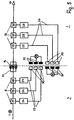
- Fig. 1 schematically shows the circuit configuration of the power supply part 3 and the device. 1
- Indicated at 5 are battery cells which are parts of the battery packs. These packs may have one or more primary cells or one or more secondary cells 5.
- a charge / discharge circuit 6 is accommodated in the housing 4. Such circuits are known and are therefore not explained in detail. With this circuit 6 is also a control and monitoring of the battery cells. 5
- housing 4 has batteries or battery packs, then various control or monitoring elements can also be accommodated in the housing 4.
- a battery circuit is shown, the positive pole 7 is separated over at least two, in the embodiment via three series-connected switch 8 of output terminals 9 of a positive output pole 10, which forms a supply contact.
- the switches 8 are advantageously transistors, in particular FETs. In the illustrated embodiment, three switches 8 are provided. The number of these switches 8 depends on which hazardous area zone or division the device 1 is to be used with the power supply part 3. When used in the zone 1, two switches 8 are sufficient, while three switches 8 are provided for use in the ex-zone zone. When used in Division 1 three Schlter are provided. This redundancy of the switch 8 ensures that in case of failure of the switch 8, the reliability remains ensured.
- the negative pole 11 of the circuit is connected to a negative output terminal 12 (supply contact), which is provided with corresponding output terminals 13.
- the power supply part 3 can be used in the Ex zones 0, 1, 2 or divisions 1, 2, the two output poles 10, 12 each have three output terminals 9, 13.
- the device 1 is provided with a corresponding positive input terminal 14 (supply contact) and a corresponding negative input terminal 15 (supply contact). Both input poles 14, 15 have a number of output terminals 9, 13 corresponding number of positive input terminals 16 and negative input terminals 17.
- the positive input terminal 14 of the device 1 is at least two, in the illustrated embodiment, three in series switches 18 connected to the positive terminal 19 and the negative input terminal 15 to the negative terminal 19.
- the switches 18 are advantageously transistors, in particular FETs.
- the number of switches 18 in turn depends on which zone or division the device is to be used.
- the redundancy of the switch 18 ensures that in case of failure of one of the switches, the reliability of the device is guaranteed in each Ex area.
- At least one signal line 21 is provided for communication between the power supply part 3 and the device 1 via at least one signal line 23 of the device is conductively connected.
- These signal lines 21, 23 are advantageously bidirectional communication lines.
- the switches 8 in the form of the transistors are each controlled by drive circuits 24, which are known per se.
- the switches 18 in the form of the transistors are each controlled by drive circuits 25 in a known manner.
- the drive circuits 24, 25 operate independently of each other and control one of the transistors 8, 18, respectively.
- the control signal 26 for the drive circuits 24 is generated in the device 1 and the control signal 27 for the drive circuits 25 in the power supply part 3.
- the shorting bar 28 may be incorporated depending on the design of the contacts in different positions, such as vertical, horizontal or oblique.
- contacts 29, which are advantageously flat and made of electrically conductive, for example, metallic material.
- the short-circuiting strip 28 has a basic body 31 made of electrically insulating material, which for example has a rectangular outline.
- the contacts 29 are fastened in a suitable manner on the base body 31 of the short-circuiting strip 28.
- the contacts 29 can be glued or plugged or screwed onto the base body 28, for example.
- Another possibility is to metallize the main body 31 to form the contacts 29 (plating) or to coat galvanically.
- the contacts 29 may have any suitable shape.
- the flat contacts 29 have a sloping contact side 32 which merges at one end into an arcuate end piece 33 which extends in the direction of the upper side of the main body 31.
- the contact side 32 passes approximately at right angles into a straight end piece 34, which extends to the main body.
- the flat contacts 29 extend for example perpendicular to the longitudinal direction of the shorting bar 28th
- the contacts 29 are advantageously identical to one another and are at a distance, advantageously at the same distance, next to each other ( 6 and 7 ).
- the main body 31 of the shorting bar 28 is provided with a top 35 which according to Fig. 6 has an exemplary rectangular outline, but is slightly smaller than the main body 31. Seen in plan view on the shorting bar 28 ( Fig. 6 ), Thus, the peripheral edge of the attachment 35 has a small distance from the peripheral edge of the body 31.
- the top of the attachment 35 extends obliquely, as in particular Fig. 8 shows.
- the removable form of the shorting bar 28 is not intended to be limiting. It may have any other suitable design and shape, depending on how the power supply part 3 and / or the device 1 are formed.
- the interacting with the contacts 29 contact elements 30 are located on a contact strip 36, as exemplified in the Fig. 9 to 11 is shown.
- the contact strip 36 has a main body 37, which consists of electrically insulating material, such as plastic, and in the mounting holes 37 'are provided. It has an example approximately rectangular shape and is provided with through holes 38 through which the contact elements 30 protrude. They are advantageously designed as spring contact pins. They protrude beyond the upper side 39 of the main body 37.
- the contact elements 30 have spherical contact surfaces 40, whereby a reliable contact with the contacts 29 is ensured.
- the other End of the contact elements 30 is located within a recess 41 in the bottom 42 of the body 37. Thus, the contact elements 30 are not on the bottom 42 of the body 37 before.
- the contact elements 30 are arranged by way of example in two rows at a distance next to and behind each other. This is only an exemplary distribution and arrangement of the contact elements 30. The respective position of the contact elements depends on the position of the contacts 29 of the short-circuiting strip 28.
- the contact elements 30 are secured in the through holes 38 in a suitable manner, for example glued or pressed.
- control lines 43, 44 ( Fig. 1 and 2 ), with which the control signals 26, 27 are supplied via the contacts 29 to the drive circuits 24, 25 ( Fig. 1 and 2 ).
- control lines 43, 44 are advantageously connectors 45, 46, so that when removing the power supply part 3 from the device 1, the signal connection to the drive circuits 24, 25 is interrupted.
- the connectors 45, 46 are located in the power supply part 3.
- the switches 8 are enabled by the device-side control signals 26 via the drive circuits 24.
- the switches 18 are enabled by the control signals 27 of the power supply part 3 via the drive circuits 25. This type of circuit ensures that without the control signal 26 of the device 1, the output pole 10 and without the control signal 27 of the power supply part 3 of the input 14 of the device 1 remains closed.
- the output terminals 9, 13 and the input terminals 16, 17 are each provided in triplicate and can be opposite to the connectors 22, 45, 46 or be designed nacheilend, so that they are not contacted simultaneously during installation or removal of the power supply part 3 or from each other. It is also possible, the output terminals 9, 13 and the input terminals 16, 17 perform opposite to each other or lagging.
- the control signals 26, 27 are supplied independently to the respective drive circuits 24, 25.
- the control lines 43, 44 are insulated from each other, so that the control signals 26, 27 can be fed undisturbed to the respective drive circuit 24, 25.
- the control signals 26, 27 have electrically different potential.
- the drive circuits 24, 25 may be discretely constructed from respective electrical / electronic components. But they can also be present as integrated circuits.
- the contacts 29 of the shorting bar 28 are also isolated from each other, so that there is no connection to other circuit parts of the device 1 and the power supply part 3.
- the supply of the control signals 26, 27 to the drive circuits 24, 25 takes place with the aid of the contact elements 30 of the contact strip 36.
- the control signals 26, 27 are supplied to the drive circuits 24, 25 in isolation from other signals.
- the power supply part 3 is located. If the power supply part 3 to the receiving compartment 2 are removed, is a multi-stage form of expression, based on the Fig. 12 to 15 is explained, ensures that the power supply part can only be removed when the supply contacts 10, 14; 12, 15 between the power supply part and the device 1 are energized or de-energized. As a result, no spark can occur when removing the power supply part 3.
- the supply of the control signals 26, 27 to the associated drive circuits 24, 25 may also be effected by switches or contact spring tongues, which are mounted on a bar or directly in / on the housing 4 of the power supply part 3 or in / on the housing of the device 1.
- Fig. 3 In the embodiment according to Fig. 3 are provided instead of the immediately coming into contact with each other contacts 29 and contact elements 30 magnets 47 and 48 magnetic sensors.
- the control signals 26, 27 are generated by magnetic excitation and supplied from the magnetic sensors 48 to the drive circuits 24, 25.
- the device 1 and the power supply part 3 are each provided with three magnets 47 and three magnetic sensors 48. If the power supply part 3 is inserted into the receptacle 2 of the device 1, the magnetic sensors 48 detect the respective magnets 47 and thereby generate the control signals 26, 27.
- the switches 8, 18 are enabled in the form of transistors via a mutual entanglement , so that in turn it is ensured that the supply contacts 10, 14; 12, 13 remain closed when the control signals 26, 27 are not triggered.
- the magnets 47 located in the power supply part 3 are detected by the corresponding, independently operating magnetic sensors 48 in the device 1.
- the independently operating magnetic sensors 48 in the power supply part 3 detect the corresponding magnets 47 in the device 1.
- the magnets 47 which are permanent magnets, and the magnetic sensors 48 work together without contact.
- the circuit of this embodiment is the same and operates in the same manner as in the previous embodiment.
- the control signals 26, 27 are generated inductively.
- the magnets 47 and proximity sensors 49 are provided.
- the device 1 and the power supply part 3 each have three permanent magnets 47 and three proximity sensors 49.
- the proximity sensors 49 are connected to a respective one of the drive circuits 24, 25.
- proximity sensors 49 that are energized upon the approach of metals, such as iron, may be used.
- the triggering elements 47 could be metal pieces or surfaces. When these metal pieces 47 approach the proximity sensors 49, the control signals 26, 27 are generated.
- the proximity sensors 49 of the energy supply part 3 approach the permanent magnet 47 of the device 1 and the permanent magnets 47 of the energy supply part 3 approach the proximity sensors 49 of the device 1.
- the proximity sensors 49 operate independently of each other.
- Fig. 5 shows an embodiment in which the control signals 26, 27 are capacitively generated.
- the device 1 and the power supply part 3 each have the proximity sensors 50 which generate the control signals 26, 27 and supply the drive circuits 24, 25 independently of each other.
- the device 1 and the power supply part 3 are also provided with capacitively exciting surfaces 51 which face the respective proximity sensors 50 when the power supply part 3 is inserted. As these surfaces 51 approach the proximity sensors 50, the control signals 26, 27 are generated. The potential 52 of the power supply part 3 provided capacitively exciting surfaces 51 is generated in the power supply part 3. The potential 53 of the capacitively exciting surfaces 51 in the device 1 is generated in the device.
- Fig. 12 shows the power supply part 3 in side view.
- the flat contacts 29 On the rear side 54 of the power supply part 3 are the flat contacts 29, which are arranged in series next to each other. If the power supply part 3 is inserted into the receiving compartment 2 of the device 1, the contacts 29 are in engagement with the device-side contact elements 30, which are provided on the contact strip 36. The contact elements 30 project beyond the rear side 54 of the power supply part 3 facing side wall 55 of the receiving compartment 2.
- the contacts 29 are located by way of example in half the width of the rear wall 54 (FIG. Fig. 12 ). On both sides of the contacts 29 54 slide guides 56, 57 are provided in the rear wall, which are advantageously formed as depressions in the rear wall 54.
- the two slotted guides 56, 57 are mirror-symmetrical to each other in the example given, in order to produce a reverse rotation of the opening movement.
- a pin 58, 59 which on sliders 60, 61 (FIG. Fig. 13 ) is provided.
- the slider 60, 61 are arranged on one side 62 of the device 1 adjacent to the receiving compartment 2.
- the slides 60, 61 are recessed in the side 62.
- the pins 58, 59 are from the sliders 60, 61 inwardly from that they protrude into the slotted guides 56, 57 of the power supply part 3.
- the pins 58, 59 are in an upper horizontal portion 63, 64 of the two Slotted guides 56, 57. In this position, the sliders 60, 61 are shifted so far toward each other that they have the smallest distance from each other.
- the two slides 60, 61 are opposite to each other in the direction of arrow 1 (FIG. FIGS. 12 and 13 ) postponed.
- the pins 58, 59 provided on the slides 60, 61 pass into a vertical section 65, 66 of the slide guides 56, 57.
- the slides 60, 61 can then no longer be displaced oppositely to one another.
- the power supply part 3 is then by means of a handle 67 in the direction of arrow 2 ( Fig. 14 ) raised.
- the slotted guides 56, 57 move relative to the located in the vertical sections 65, 66 pins 58, 59, until they reach a lower horizontal portion 68, 69 of the slotted guides. Then the energy supply part can no longer be raised ( Fig. 14 ).
- the lower horizontal portions 68, 69 then go into vertically downwardly extending end portions 70, 71, which are open to the bottom 72 of the power supply part 3. This makes it possible to completely remove the power supply part 3 from the receiving compartment 2.
- the power supply part 3 is overlapped on the opposite side by a tab 73. It ensures that the power supply part 3 can be removed from the receiving compartment 2 only by the described pivoting movement.
- the multistage shape mimic described ensures that the power supply part 3 can be removed from the receiving compartment 2 only after a multi-stage unlocking process. This ensures that initially the control signals 26, 27 generating circuit 29, 30; 47, 48; 47, 49; 50, 51 the supply contacts 10, 14; 12, 15 switched off. This happens in the embodiment of the Fig. 1 and 2 in that the contact elements 30 in the form of the spring contact pins are disengaged from the contacts 29. In the embodiments according to the Fig. 3 to 5 the magnets 47 and the capacitively exciting surfaces 51 are removed by the proximity sensors 49, 50. Only upon complete removal of the power supply part 3, the supply contacts 10, 14; 12, 15 separated from each other. Since they are now dead, no spark when removing the power supply part 3 can arise.
- the power supply part 3 does not have to be able to be inserted into a receiving compartment 2 in the manner described. It is also conceivable to use the power supply in a slot. In this case, the power supply part 3 is pushed into the device 1. Even then it can be ensured that when pulling out of the power supply part 3, first the supply contacts 10, 14; 12, 15 are de-energized before the power supply is completely pulled out.
- a multi-level form of expression can be provided in the side walls of the insertion compartment.
Landscapes
- Engineering & Computer Science (AREA)
- Chemical & Material Sciences (AREA)
- Chemical Kinetics & Catalysis (AREA)
- Electrochemistry (AREA)
- General Chemical & Material Sciences (AREA)
- Microelectronics & Electronic Packaging (AREA)
- Manufacturing & Machinery (AREA)
- Power Engineering (AREA)
- Portable Nailing Machines And Staplers (AREA)
- Details Of Connecting Devices For Male And Female Coupling (AREA)
- Battery Mounting, Suspending (AREA)
- Charge And Discharge Circuits For Batteries Or The Like (AREA)
Applications Claiming Priority (1)
| Application Number | Priority Date | Filing Date | Title |
|---|---|---|---|
| DE102017010107.8A DE102017010107A1 (de) | 2017-10-26 | 2017-10-26 | Gerät zum Einsatz im Ex-Bereich |
Publications (3)
| Publication Number | Publication Date |
|---|---|
| EP3477790A2 true EP3477790A2 (fr) | 2019-05-01 |
| EP3477790A3 EP3477790A3 (fr) | 2019-07-24 |
| EP3477790B1 EP3477790B1 (fr) | 2023-10-04 |
Family
ID=63878303
Family Applications (1)
| Application Number | Title | Priority Date | Filing Date |
|---|---|---|---|
| EP18000811.2A Active EP3477790B1 (fr) | 2017-10-26 | 2018-10-15 | Appareil à utiliser dans une zone à risque d'explosion |
Country Status (6)
| Country | Link |
|---|---|
| US (1) | US10897108B2 (fr) |
| EP (1) | EP3477790B1 (fr) |
| AU (1) | AU2018250434B2 (fr) |
| DE (1) | DE102017010107A1 (fr) |
| TW (1) | TWI710191B (fr) |
| ZA (1) | ZA201806187B (fr) |
Families Citing this family (1)
| Publication number | Priority date | Publication date | Assignee | Title |
|---|---|---|---|---|
| DE102024119228A1 (de) * | 2024-07-05 | 2026-01-08 | Einhell Germany Ag | Akkumulator für Arbeitsgeräte |
Family Cites Families (12)
| Publication number | Priority date | Publication date | Assignee | Title |
|---|---|---|---|---|
| DE2740160A1 (de) * | 1977-09-02 | 1979-03-08 | Auergesellschaft Gmbh | Stromversorgungsteil fuer messgeraete |
| DE19748553A1 (de) * | 1997-11-04 | 1999-05-20 | Aeg Starkstrom Anlagenbau Magd | Einschub für einen elektrischen Schaltschrank |
| DE19838492A1 (de) * | 1998-08-25 | 2000-03-09 | Stahl R Schaltgeraete Gmbh | Explosionsgeschützte Steckverbindungsanordnung |
| DE10049346A1 (de) * | 1999-10-08 | 2001-04-12 | Tyco Electronics Amp Gmbh | Steckeranordnung mit einem schwenkbaren Deckel |
| US7550943B2 (en) * | 2006-09-19 | 2009-06-23 | Eveready Battery Company, Inc. | Intrinsically safe battery-powered device |
| DE102006047039A1 (de) * | 2006-10-02 | 2007-11-08 | Leoni Bordnetz-Systeme Gmbh | Kontaktverbindung, insbesondere zur lösbaren elektrischen Anbindung eines elektrischen Antriebsmotors eines Kraftfahrzeugs |
| TW200937788A (en) * | 2008-02-29 | 2009-09-01 | Chaun-Yuan Chen | An overheat safety protection of power supply socket when overloaded |
| TW201004098A (en) * | 2008-07-14 | 2010-01-16 | Lite On Technology Corp | Energy storage device, access device, and a combination thereof |
| US8094426B2 (en) * | 2009-06-02 | 2012-01-10 | Eaton Corporation | Electrical switching apparatus providing coordinated opening with a circuit interrupter and method of operating the same |
| DE102013213042B4 (de) * | 2013-07-04 | 2022-05-25 | Ecom Instruments Gmbh | Elektronische Schaltungsanordnung zur Verwendung in einem explosionsgefährdeten Bereich |
| DE102013219950B4 (de) | 2013-10-01 | 2018-12-13 | Ecom Instruments Gmbh | Elektronische Schaltungsanordnung |
| JP6660696B2 (ja) * | 2015-09-17 | 2020-03-11 | 三菱重工業株式会社 | 防爆機器 |
-
2017
- 2017-10-26 DE DE102017010107.8A patent/DE102017010107A1/de not_active Withdrawn
-
2018
- 2018-09-14 ZA ZA2018/06187A patent/ZA201806187B/en unknown
- 2018-09-19 TW TW107132992A patent/TWI710191B/zh not_active IP Right Cessation
- 2018-10-15 EP EP18000811.2A patent/EP3477790B1/fr active Active
- 2018-10-18 AU AU2018250434A patent/AU2018250434B2/en active Active
- 2018-10-19 US US16/165,218 patent/US10897108B2/en active Active
Non-Patent Citations (1)
| Title |
|---|
| None |
Also Published As
| Publication number | Publication date |
|---|---|
| US10897108B2 (en) | 2021-01-19 |
| TWI710191B (zh) | 2020-11-11 |
| TW201924171A (zh) | 2019-06-16 |
| EP3477790B1 (fr) | 2023-10-04 |
| ZA201806187B (en) | 2022-03-30 |
| AU2018250434B2 (en) | 2021-09-30 |
| AU2018250434A1 (en) | 2019-05-16 |
| DE102017010107A1 (de) | 2019-05-16 |
| US20190131750A1 (en) | 2019-05-02 |
| EP3477790A3 (fr) | 2019-07-24 |
Similar Documents
| Publication | Publication Date | Title |
|---|---|---|
| DE102004054360B4 (de) | Elektrische Steckverbinderkupplung mit Schaltfunktion | |
| EP2909059B1 (fr) | Dispositif de charge d'un véhicule électrique à une borne de recharge | |
| DE1048189B (de) | Elektrischer Rasierapparat | |
| DE2730660A1 (de) | Elektrische kupplungsvorrichtung | |
| WO2008135183A1 (fr) | Dispositif de contrôle de la fixation d'une carte de circuits imprimés sur un support | |
| DE102010063783A1 (de) | Feldgerät mit einer Batterieeinheit | |
| EP2715871A1 (fr) | Ensemble dispositif de contrôle et de connexion et dispositif de connexion | |
| DE69834450T2 (de) | Fernsehkamera | |
| DE10003267C2 (de) | Stromkreisunterbrechereinrichtung | |
| DE202018006661U1 (de) | Modularer Steckverbinder austauschbarer Modul-Leiterplatte | |
| DE102021110929A1 (de) | System und verfahren zum autonomen laden eines elektrofahrzeugs | |
| EP1131987A1 (fr) | Systeme de montage pour cartes imprimees electriques avec contacts de centrage sur des elements frontaux et contacts de reception distincts en particulier avec des lames de contact dans le chassis | |
| EP3477790B1 (fr) | Appareil à utiliser dans une zone à risque d'explosion | |
| DE2046430B2 (de) | Prüfanordnung | |
| DE69508055T2 (de) | Apparat mit unterdrückung von transienten spannungen | |
| EP3032694A1 (fr) | Pack batterie à capacité totale commutable | |
| DE10040893A1 (de) | Struktur von elektrischen Anschlüssen zum Herstellen eines elektrischen Kontakts zwischen einem Batterieteil und einer elektrischen Vorrichtung | |
| DE102020003168A1 (de) | Energiespeicher mit Gehäuse und Brückenstecker | |
| DE4407083A1 (de) | Verbindungsstecker | |
| DE19748553A1 (de) | Einschub für einen elektrischen Schaltschrank | |
| EP4525218A1 (fr) | Système de connecteur et système de distribution d'énergie électrique | |
| EP3214415B1 (fr) | Capteur comprenant un microprocesseur et procédé de fourniture et d'introduction d'un signal de capteur dans un bus d'installation d'un dispositif d'automatisation de bâtiment | |
| DE202016107303U1 (de) | Batterieklemme, Batterieklemmenanordnung und Batterieaufnahme für einen Handsender für Gebäude- oder Einfriedungsabschlusssysteme | |
| DE20023631U1 (de) | Struktur von elektrischen Anschlüssen zum Herstellen eines elektrischen Kontakts zwischen einem Batterieteil und einer elektrischen Vorrichtung | |
| DE102024127324A1 (de) | Anschlusssystem zum elektrischen Verbinden zweier Hochspannungskomponenten und Kraftfahrzeug damit |
Legal Events
| Date | Code | Title | Description |
|---|---|---|---|
| PUAI | Public reference made under article 153(3) epc to a published international application that has entered the european phase |
Free format text: ORIGINAL CODE: 0009012 |
|
| STAA | Information on the status of an ep patent application or granted ep patent |
Free format text: STATUS: THE APPLICATION HAS BEEN PUBLISHED |
|
| AK | Designated contracting states |
Kind code of ref document: A2 Designated state(s): AL AT BE BG CH CY CZ DE DK EE ES FI FR GB GR HR HU IE IS IT LI LT LU LV MC MK MT NL NO PL PT RO RS SE SI SK SM TR |
|
| AX | Request for extension of the european patent |
Extension state: BA ME |
|
| PUAL | Search report despatched |
Free format text: ORIGINAL CODE: 0009013 |
|
| AK | Designated contracting states |
Kind code of ref document: A3 Designated state(s): AL AT BE BG CH CY CZ DE DK EE ES FI FR GB GR HR HU IE IS IT LI LT LU LV MC MK MT NL NO PL PT RO RS SE SI SK SM TR |
|
| AX | Request for extension of the european patent |
Extension state: BA ME |
|
| RIC1 | Information provided on ipc code assigned before grant |
Ipc: H03K 17/10 20060101ALI20190620BHEP Ipc: H01R 13/703 20060101AFI20190620BHEP |
|
| STAA | Information on the status of an ep patent application or granted ep patent |
Free format text: STATUS: REQUEST FOR EXAMINATION WAS MADE |
|
| 17P | Request for examination filed |
Effective date: 20200120 |
|
| RBV | Designated contracting states (corrected) |
Designated state(s): AL AT BE BG CH CY CZ DE DK EE ES FI FR GB GR HR HU IE IS IT LI LT LU LV MC MK MT NL NO PL PT RO RS SE SI SK SM TR |
|
| REG | Reference to a national code |
Ref legal event code: R079 Free format text: PREVIOUS MAIN CLASS: H01R0013703000 Ipc: H03K0017100000 Ref country code: DE Ref legal event code: R079 Ref document number: 502018013353 Country of ref document: DE Free format text: PREVIOUS MAIN CLASS: H01R0013703000 Ipc: H03K0017100000 |
|
| GRAP | Despatch of communication of intention to grant a patent |
Free format text: ORIGINAL CODE: EPIDOSNIGR1 |
|
| STAA | Information on the status of an ep patent application or granted ep patent |
Free format text: STATUS: GRANT OF PATENT IS INTENDED |
|
| RIC1 | Information provided on ipc code assigned before grant |
Ipc: H01M 50/574 20210101ALI20230316BHEP Ipc: H01R 13/703 20060101ALI20230316BHEP Ipc: H03K 17/10 20060101AFI20230316BHEP |
|
| INTG | Intention to grant announced |
Effective date: 20230417 |
|
| GRAS | Grant fee paid |
Free format text: ORIGINAL CODE: EPIDOSNIGR3 |
|
| GRAA | (expected) grant |
Free format text: ORIGINAL CODE: 0009210 |
|
| STAA | Information on the status of an ep patent application or granted ep patent |
Free format text: STATUS: THE PATENT HAS BEEN GRANTED |
|
| AK | Designated contracting states |
Kind code of ref document: B1 Designated state(s): AL AT BE BG CH CY CZ DE DK EE ES FI FR GB GR HR HU IE IS IT LI LT LU LV MC MK MT NL NO PL PT RO RS SE SI SK SM TR |
|
| REG | Reference to a national code |
Ref country code: GB Ref legal event code: FG4D Free format text: NOT ENGLISH |
|
| REG | Reference to a national code |
Ref country code: CH Ref legal event code: EP |
|
| REG | Reference to a national code |
Ref country code: IE Ref legal event code: FG4D Free format text: LANGUAGE OF EP DOCUMENT: GERMAN |
|
| REG | Reference to a national code |
Ref country code: DE Ref legal event code: R096 Ref document number: 502018013353 Country of ref document: DE |
|
| REG | Reference to a national code |
Ref country code: LT Ref legal event code: MG9D |
|
| REG | Reference to a national code |
Ref country code: NL Ref legal event code: MP Effective date: 20231004 |
|
| PG25 | Lapsed in a contracting state [announced via postgrant information from national office to epo] |
Ref country code: NL Free format text: LAPSE BECAUSE OF FAILURE TO SUBMIT A TRANSLATION OF THE DESCRIPTION OR TO PAY THE FEE WITHIN THE PRESCRIBED TIME-LIMIT Effective date: 20231004 |
|
| PG25 | Lapsed in a contracting state [announced via postgrant information from national office to epo] |
Ref country code: GR Free format text: LAPSE BECAUSE OF FAILURE TO SUBMIT A TRANSLATION OF THE DESCRIPTION OR TO PAY THE FEE WITHIN THE PRESCRIBED TIME-LIMIT Effective date: 20240105 |
|
| PG25 | Lapsed in a contracting state [announced via postgrant information from national office to epo] |
Ref country code: IS Free format text: LAPSE BECAUSE OF FAILURE TO SUBMIT A TRANSLATION OF THE DESCRIPTION OR TO PAY THE FEE WITHIN THE PRESCRIBED TIME-LIMIT Effective date: 20240204 |
|
| PG25 | Lapsed in a contracting state [announced via postgrant information from national office to epo] |
Ref country code: LT Free format text: LAPSE BECAUSE OF FAILURE TO SUBMIT A TRANSLATION OF THE DESCRIPTION OR TO PAY THE FEE WITHIN THE PRESCRIBED TIME-LIMIT Effective date: 20231004 |
|
| PG25 | Lapsed in a contracting state [announced via postgrant information from national office to epo] |
Ref country code: ES Free format text: LAPSE BECAUSE OF FAILURE TO SUBMIT A TRANSLATION OF THE DESCRIPTION OR TO PAY THE FEE WITHIN THE PRESCRIBED TIME-LIMIT Effective date: 20231004 |
|
| PG25 | Lapsed in a contracting state [announced via postgrant information from national office to epo] |
Ref country code: LT Free format text: LAPSE BECAUSE OF FAILURE TO SUBMIT A TRANSLATION OF THE DESCRIPTION OR TO PAY THE FEE WITHIN THE PRESCRIBED TIME-LIMIT Effective date: 20231004 Ref country code: IS Free format text: LAPSE BECAUSE OF FAILURE TO SUBMIT A TRANSLATION OF THE DESCRIPTION OR TO PAY THE FEE WITHIN THE PRESCRIBED TIME-LIMIT Effective date: 20240204 Ref country code: GR Free format text: LAPSE BECAUSE OF FAILURE TO SUBMIT A TRANSLATION OF THE DESCRIPTION OR TO PAY THE FEE WITHIN THE PRESCRIBED TIME-LIMIT Effective date: 20240105 Ref country code: ES Free format text: LAPSE BECAUSE OF FAILURE TO SUBMIT A TRANSLATION OF THE DESCRIPTION OR TO PAY THE FEE WITHIN THE PRESCRIBED TIME-LIMIT Effective date: 20231004 Ref country code: BG Free format text: LAPSE BECAUSE OF FAILURE TO SUBMIT A TRANSLATION OF THE DESCRIPTION OR TO PAY THE FEE WITHIN THE PRESCRIBED TIME-LIMIT Effective date: 20240104 Ref country code: PT Free format text: LAPSE BECAUSE OF FAILURE TO SUBMIT A TRANSLATION OF THE DESCRIPTION OR TO PAY THE FEE WITHIN THE PRESCRIBED TIME-LIMIT Effective date: 20240205 |
|
| PG25 | Lapsed in a contracting state [announced via postgrant information from national office to epo] |
Ref country code: SE Free format text: LAPSE BECAUSE OF FAILURE TO SUBMIT A TRANSLATION OF THE DESCRIPTION OR TO PAY THE FEE WITHIN THE PRESCRIBED TIME-LIMIT Effective date: 20231004 Ref country code: RS Free format text: LAPSE BECAUSE OF FAILURE TO SUBMIT A TRANSLATION OF THE DESCRIPTION OR TO PAY THE FEE WITHIN THE PRESCRIBED TIME-LIMIT Effective date: 20231004 Ref country code: PL Free format text: LAPSE BECAUSE OF FAILURE TO SUBMIT A TRANSLATION OF THE DESCRIPTION OR TO PAY THE FEE WITHIN THE PRESCRIBED TIME-LIMIT Effective date: 20231004 Ref country code: NO Free format text: LAPSE BECAUSE OF FAILURE TO SUBMIT A TRANSLATION OF THE DESCRIPTION OR TO PAY THE FEE WITHIN THE PRESCRIBED TIME-LIMIT Effective date: 20240104 Ref country code: LV Free format text: LAPSE BECAUSE OF FAILURE TO SUBMIT A TRANSLATION OF THE DESCRIPTION OR TO PAY THE FEE WITHIN THE PRESCRIBED TIME-LIMIT Effective date: 20231004 Ref country code: HR Free format text: LAPSE BECAUSE OF FAILURE TO SUBMIT A TRANSLATION OF THE DESCRIPTION OR TO PAY THE FEE WITHIN THE PRESCRIBED TIME-LIMIT Effective date: 20231004 |
|
| REG | Reference to a national code |
Ref country code: CH Ref legal event code: PL |
|
| REG | Reference to a national code |
Ref country code: BE Ref legal event code: MM Effective date: 20231031 |
|
| PG25 | Lapsed in a contracting state [announced via postgrant information from national office to epo] |
Ref country code: LU Free format text: LAPSE BECAUSE OF NON-PAYMENT OF DUE FEES Effective date: 20231015 |
|
| PG25 | Lapsed in a contracting state [announced via postgrant information from national office to epo] |
Ref country code: LU Free format text: LAPSE BECAUSE OF NON-PAYMENT OF DUE FEES Effective date: 20231015 |
|
| REG | Reference to a national code |
Ref country code: DE Ref legal event code: R097 Ref document number: 502018013353 Country of ref document: DE |
|
| PG25 | Lapsed in a contracting state [announced via postgrant information from national office to epo] |
Ref country code: DK Free format text: LAPSE BECAUSE OF FAILURE TO SUBMIT A TRANSLATION OF THE DESCRIPTION OR TO PAY THE FEE WITHIN THE PRESCRIBED TIME-LIMIT Effective date: 20231004 |
|
| PG25 | Lapsed in a contracting state [announced via postgrant information from national office to epo] |
Ref country code: CH Free format text: LAPSE BECAUSE OF NON-PAYMENT OF DUE FEES Effective date: 20231031 |
|
| PG25 | Lapsed in a contracting state [announced via postgrant information from national office to epo] |
Ref country code: CZ Free format text: LAPSE BECAUSE OF FAILURE TO SUBMIT A TRANSLATION OF THE DESCRIPTION OR TO PAY THE FEE WITHIN THE PRESCRIBED TIME-LIMIT Effective date: 20231004 |
|
| PG25 | Lapsed in a contracting state [announced via postgrant information from national office to epo] |
Ref country code: SK Free format text: LAPSE BECAUSE OF FAILURE TO SUBMIT A TRANSLATION OF THE DESCRIPTION OR TO PAY THE FEE WITHIN THE PRESCRIBED TIME-LIMIT Effective date: 20231004 |
|
| PG25 | Lapsed in a contracting state [announced via postgrant information from national office to epo] |
Ref country code: SM Free format text: LAPSE BECAUSE OF FAILURE TO SUBMIT A TRANSLATION OF THE DESCRIPTION OR TO PAY THE FEE WITHIN THE PRESCRIBED TIME-LIMIT Effective date: 20231004 Ref country code: SK Free format text: LAPSE BECAUSE OF FAILURE TO SUBMIT A TRANSLATION OF THE DESCRIPTION OR TO PAY THE FEE WITHIN THE PRESCRIBED TIME-LIMIT Effective date: 20231004 Ref country code: RO Free format text: LAPSE BECAUSE OF FAILURE TO SUBMIT A TRANSLATION OF THE DESCRIPTION OR TO PAY THE FEE WITHIN THE PRESCRIBED TIME-LIMIT Effective date: 20231004 Ref country code: IT Free format text: LAPSE BECAUSE OF FAILURE TO SUBMIT A TRANSLATION OF THE DESCRIPTION OR TO PAY THE FEE WITHIN THE PRESCRIBED TIME-LIMIT Effective date: 20231004 Ref country code: EE Free format text: LAPSE BECAUSE OF FAILURE TO SUBMIT A TRANSLATION OF THE DESCRIPTION OR TO PAY THE FEE WITHIN THE PRESCRIBED TIME-LIMIT Effective date: 20231004 Ref country code: DK Free format text: LAPSE BECAUSE OF FAILURE TO SUBMIT A TRANSLATION OF THE DESCRIPTION OR TO PAY THE FEE WITHIN THE PRESCRIBED TIME-LIMIT Effective date: 20231004 Ref country code: CZ Free format text: LAPSE BECAUSE OF FAILURE TO SUBMIT A TRANSLATION OF THE DESCRIPTION OR TO PAY THE FEE WITHIN THE PRESCRIBED TIME-LIMIT Effective date: 20231004 Ref country code: CH Free format text: LAPSE BECAUSE OF NON-PAYMENT OF DUE FEES Effective date: 20231031 |
|
| PLBE | No opposition filed within time limit |
Free format text: ORIGINAL CODE: 0009261 |
|
| STAA | Information on the status of an ep patent application or granted ep patent |
Free format text: STATUS: NO OPPOSITION FILED WITHIN TIME LIMIT |
|
| PG25 | Lapsed in a contracting state [announced via postgrant information from national office to epo] |
Ref country code: MC Free format text: LAPSE BECAUSE OF FAILURE TO SUBMIT A TRANSLATION OF THE DESCRIPTION OR TO PAY THE FEE WITHIN THE PRESCRIBED TIME-LIMIT Effective date: 20231004 |
|
| PG25 | Lapsed in a contracting state [announced via postgrant information from national office to epo] |
Ref country code: MC Free format text: LAPSE BECAUSE OF FAILURE TO SUBMIT A TRANSLATION OF THE DESCRIPTION OR TO PAY THE FEE WITHIN THE PRESCRIBED TIME-LIMIT Effective date: 20231004 Ref country code: BE Free format text: LAPSE BECAUSE OF NON-PAYMENT OF DUE FEES Effective date: 20231031 |
|
| 26N | No opposition filed |
Effective date: 20240705 |
|
| PG25 | Lapsed in a contracting state [announced via postgrant information from national office to epo] |
Ref country code: IE Free format text: LAPSE BECAUSE OF NON-PAYMENT OF DUE FEES Effective date: 20231015 |
|
| PG25 | Lapsed in a contracting state [announced via postgrant information from national office to epo] |
Ref country code: SI Free format text: LAPSE BECAUSE OF FAILURE TO SUBMIT A TRANSLATION OF THE DESCRIPTION OR TO PAY THE FEE WITHIN THE PRESCRIBED TIME-LIMIT Effective date: 20231004 |
|
| PG25 | Lapsed in a contracting state [announced via postgrant information from national office to epo] |
Ref country code: SI Free format text: LAPSE BECAUSE OF FAILURE TO SUBMIT A TRANSLATION OF THE DESCRIPTION OR TO PAY THE FEE WITHIN THE PRESCRIBED TIME-LIMIT Effective date: 20231004 Ref country code: IE Free format text: LAPSE BECAUSE OF NON-PAYMENT OF DUE FEES Effective date: 20231015 |
|
| REG | Reference to a national code |
Ref country code: AT Ref legal event code: MM01 Ref document number: 1618810 Country of ref document: AT Kind code of ref document: T Effective date: 20231015 |
|
| PG25 | Lapsed in a contracting state [announced via postgrant information from national office to epo] |
Ref country code: AT Free format text: LAPSE BECAUSE OF NON-PAYMENT OF DUE FEES Effective date: 20231015 |
|
| PG25 | Lapsed in a contracting state [announced via postgrant information from national office to epo] |
Ref country code: AT Free format text: LAPSE BECAUSE OF NON-PAYMENT OF DUE FEES Effective date: 20231015 |
|
| PG25 | Lapsed in a contracting state [announced via postgrant information from national office to epo] |
Ref country code: FI Free format text: LAPSE BECAUSE OF FAILURE TO SUBMIT A TRANSLATION OF THE DESCRIPTION OR TO PAY THE FEE WITHIN THE PRESCRIBED TIME-LIMIT Effective date: 20231004 |
|
| PG25 | Lapsed in a contracting state [announced via postgrant information from national office to epo] |
Ref country code: CY Free format text: LAPSE BECAUSE OF FAILURE TO SUBMIT A TRANSLATION OF THE DESCRIPTION OR TO PAY THE FEE WITHIN THE PRESCRIBED TIME-LIMIT; INVALID AB INITIO Effective date: 20181015 |
|
| PG25 | Lapsed in a contracting state [announced via postgrant information from national office to epo] |
Ref country code: HU Free format text: LAPSE BECAUSE OF FAILURE TO SUBMIT A TRANSLATION OF THE DESCRIPTION OR TO PAY THE FEE WITHIN THE PRESCRIBED TIME-LIMIT; INVALID AB INITIO Effective date: 20181015 |
|
| PGFP | Annual fee paid to national office [announced via postgrant information from national office to epo] |
Ref country code: GB Payment date: 20250922 Year of fee payment: 8 |
|
| PG25 | Lapsed in a contracting state [announced via postgrant information from national office to epo] |
Ref country code: TR Free format text: LAPSE BECAUSE OF FAILURE TO SUBMIT A TRANSLATION OF THE DESCRIPTION OR TO PAY THE FEE WITHIN THE PRESCRIBED TIME-LIMIT Effective date: 20231004 |
|
| PGFP | Annual fee paid to national office [announced via postgrant information from national office to epo] |
Ref country code: DE Payment date: 20251029 Year of fee payment: 8 |
|
| PGFP | Annual fee paid to national office [announced via postgrant information from national office to epo] |
Ref country code: FR Payment date: 20251001 Year of fee payment: 8 |