EP3477800B1 - Procédé de production d'une bougie d'allumage - Google Patents
Procédé de production d'une bougie d'allumage Download PDFInfo
- Publication number
- EP3477800B1 EP3477800B1 EP17815012.4A EP17815012A EP3477800B1 EP 3477800 B1 EP3477800 B1 EP 3477800B1 EP 17815012 A EP17815012 A EP 17815012A EP 3477800 B1 EP3477800 B1 EP 3477800B1
- Authority
- EP
- European Patent Office
- Prior art keywords
- electrode
- base material
- electrode base
- tip
- contact
- Prior art date
- Legal status (The legal status is an assumption and is not a legal conclusion. Google has not performed a legal analysis and makes no representation as to the accuracy of the status listed.)
- Active
Links
Images

Classifications
-
- H—ELECTRICITY
- H01—ELECTRIC ELEMENTS
- H01T—SPARK GAPS; OVERVOLTAGE ARRESTERS USING SPARK GAPS; SPARKING PLUGS; CORONA DEVICES; GENERATING IONS TO BE INTRODUCED INTO NON-ENCLOSED GASES
- H01T13/00—Sparking plugs
- H01T13/20—Sparking plugs characterised by features of the electrodes or insulation
- H01T13/32—Sparking plugs characterised by features of the electrodes or insulation characterised by features of the earthed electrode
-
- H—ELECTRICITY
- H01—ELECTRIC ELEMENTS
- H01T—SPARK GAPS; OVERVOLTAGE ARRESTERS USING SPARK GAPS; SPARKING PLUGS; CORONA DEVICES; GENERATING IONS TO BE INTRODUCED INTO NON-ENCLOSED GASES
- H01T21/00—Apparatus or processes specially adapted for the manufacture or maintenance of spark gaps or sparking plugs
- H01T21/02—Apparatus or processes specially adapted for the manufacture or maintenance of spark gaps or sparking plugs of sparking plugs
Definitions
- the present invention relates to a method for manufacturing a spark plug and particularly relates to a method for manufacturing a spark plug such that variations in welding of an electrode base material and a tip can be suppressed.
- a spark plug which includes: a ground electrode in which a tip containing a noble metal is joined to an electrode base material; and a center electrode opposing the ground electrode with a spark gap therebetween.
- Resistance welding is one of the methods for joining the electrode base material and the tip together. Resistance welding is performed by applying current between the first electrode and the second electrode, in a state where the electrode base material and the tip stacked with each other are in contact with a first electrode and a second electrode, respectively.
- Patent Document 1 discloses a technique in which the surface of the electrode base material is ground and then resistance welding is performed in a state where the tip is stacked on the ground surface.
- Patent Document 1 Japanese Patent Application Laid-Open ( kokai ) No. 2004-186152
- EP2667465 A1 discloses a method for manufacturing a spark plug by joining a tip containing a noble metal to an electrode base material by means of resistance welding in which current is applied between a first electrode and a second electrode, to obtain a ground electrode, the method comprising: a welding step of performing resistance welding by applying current between the first electrode and the second electrode, after bringing the first surface of the electrode base material and the tip into contact with each other, bringing the first electrode into contact with the second surface of the electrode base material, and bringing the second electrode into contact with the tip.
- JP2015153724 A discloses another example welding method for manufacturing a spark plug.
- the above-described conventional technique has the following problem.
- resistance welding the electrode base material and the tip are melted and bonded to each other by Joule heat generated by contact resistance between the electrode base material and the tip.
- variations occur in contact resistance between the electrode base material and the first electrode and contact resistance between the tip and the second electrode, variations occur in welding of the tip and the electrode base material.
- the present invention has been made in order to solve the aforementioned problem, and an object of the present invention is to provide a method for manufacturing a spark plug such that variations in welding of an electrode base material and a tip can be suppressed.
- a tip containing a noble metal is joined to an electrode base material by means of resistance welding in which current is applied between a first electrode and a second electrode, so that a ground electrode is obtained.
- a first step a first surface having an area larger than or equal to an area making contact with the tip is produced on the electrode base material by performing at least one of polishing and grinding thereon.
- a second step a second surface having an area larger than or equal to an area making contact with the first electrode is produced on the electrode base material by performing at least one of polishing and grinding thereon.
- resistance welding is performed by applying current between the first electrode and the second electrode, after the first surface of the electrode base material and the tip have been brought into contact with each other, the first electrode has been brought into contact with the second surface of the electrode base material, and the second electrode has been brought into contact with the tip. Since variations in contact resistance between the electrode base material and the first electrode and variations in contact resistance between the tip and the second electrode can be suppressed, an effect of suppressing variations in welding of the electrode base material and the tip can be obtained.
- An arithmetic average roughness of the first surface is not less than an arithmetic average roughness of the second surface. Since the Joule heat that melts the tip and the electrode base material during welding depends on the contact resistance between the first surface of the electrode base material and the tip, in a case where the arithmetic average roughness of the first surface is set to be not less than the arithmetic average roughness of the second surface, the contact resistance between the first surface of the electrode base material and the tip can be ensured. Since the Joule heat generated between the tip and the electrode base material can be ensured, an effect of ensuring joining strength between the electrode base material and the tip can be obtained.
- the arithmetic average roughness of each of the first surface and the second surface of the electrode base material is 2 to 4 ⁇ m
- the arithmetic average roughness of each of a third surface and a fourth surface of the tip is 0.4 to 0.8 ⁇ m.
- the method for manufacturing the spark plug according to a second aspect of the present invention includes an assembling step of assembling a tubular insulator and a tubular metal shell to which the electrode base material is joined, wherein after the assembling step, an electrode base material adjusting step is performed.
- an effect of further improving the joining strength between the electrode base material and the tip can be obtained.
- the method for manufacturing the spark plug according to a third aspect of the present invention includes a third step of producing the third surface on the tip by performing at least one of polishing and grinding thereon, and a fourth step of producing the fourth surface on the tip by performing at least one of polishing and grinding thereon. As a result, the arithmetic average roughness of each of the third surface and the fourth surface of the tip can be easily adjusted.
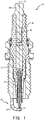
- FIG. 1 is a cross-sectional view of a spark plug 10, according to an embodiment of the present invention, taken along a plane including a central axis O thereof.
- the spark plug 10 includes a metal shell 11, a ground electrode 12, an insulator 15, a center electrode 17, and a metal terminal 18.
- the metal shell 11 is a substantially cylindrical member that is fixed in a thread hole of an internal combustion engine (not shown).
- the ground electrode 12 includes: an electrode base material 13 that is made of metal (e.g., a nickel-based alloy) and that is joined to a front end of the metal shell 11; and a tip 14 that is joined to the front end of the electrode base material 13.
- the electrode base material 13 is a rod-shaped member that is bent toward the central axis O so as to intersect the central axis O.
- the tip 14 is a plate-shaped member formed of a noble metal such as platinum, iridium, ruthenium, or rhodium, or an alloy containing such a noble metal as a principal component, and is joined to the electrode base material 13 by means of resistance welding.
- the insulator 15 is a substantially cylindrical member formed of alumina or the like that has excellent mechanical property and insulation property at a high temperature, has an axial hole 16 that penetrates therethrough along the central axis O, and has an outer circumference on which the metal shell 11 is fixed.
- the center electrode 17 is a rod-shaped electrode that is inserted into the axial hole 16 and held by the insulator 15, and opposes the tip 14 of the ground electrode 12 with a spark gap therebetween.
- the metal terminal 18 is a rod-shaped member to which a high-voltage cable (not shown) is connected, and a front side of the metal terminal 18 is disposed in the insulator 15.
- the spark plug 10 is manufactured by, for example, a method described below. Firstly, the center electrode 17 is inserted into the axial hole 16 of the insulator 15. The center electrode 17 is disposed such that the front end thereof is exposed to the outside from the front end of the axial hole 16. After the metal terminal 18 is inserted into the axial hole 16, so that electrical connection is ensured between the metal terminal 18 and the center electrode 17, the metal shell 11 to which the ground electrode 12 has been joined in advance is assembled to the outer circumference of the insulator 15. After the tip 14 has been joined to the electrode base material 13 of the ground electrode 12 by means of resistance welding, the electrode base material 13 is bent such that the tip 14 opposes the center electrode 17 in the axial direction, so that the spark plug 10 is obtained.
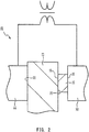
- FIG. 2 is a schematic view of a resistance welding machine 20 used in a welding step.
- a portion of the electrode base material 13 in a longitudinal direction is not shown.
- the resistance welding machine 20 includes a first electrode 21 and a second electrode 22 to both of which a transformer is connected. Welding of the electrode base material 13 and the tip 14 is performed by means of resistance welding in which current is applied between the first electrode 21 and the second electrode 22, after the electrode base material 13 and the tip 14 have been brought into contact with each other, the first electrode 21 has been brought into contact with the electrode base material 13, and the second electrode 22 has been brought into contact with the tip 14.
- a first surface 31 of the electrode base material 13 makes contact with a third surface 33 of the tip 14.
- a contact surface 21a of the first electrode 21 is brought into contact with a second surface 32 of the electrode base material 13, and a contact surface 22a of the second electrode 22 is brought into contact with a fourth surface 34 of the tip 14.
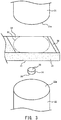
- FIG. 3 is a perspective view of the tip 14 and the electrode base material 13. In FIG. 3 , a portion of the electrode base material 13 in the longitudinal direction is not shown. FIG. 3 shows a state before resistance welding is performed.
- the electrode base material 13 has the second surface 32 and the first surface 31 that is different from the second surface 32.
- the second surface 32 is a surface having an area larger than or equal to an area 35 making contact with the contact surface 21a of the first electrode 21, and is produced by performing at least one of polishing and grinding on the electrode base material 13.
- the first surface 31 is a surface having an area larger than or equal to an area making contact with the third surface 33 of the tip 14, and is produced by performing at least one of polishing and grinding on the electrode base material 13.
- the first surface 31 is provided on a surface reverse to the second surface 32.
- the tip 14 has the fourth surface 34 on the back of the third surface 33.
- the third surface 33 is a surface having an area smaller than or equal to an area making contact with the first surface 31 of the electrode base material 13
- the fourth surface 34 is a surface having an area smaller than or equal to an area making contact with the contact surface 22a of the second electrode 22. It is noted that the third surface 33 and the fourth surface 34 may be formed by punching out a plate material having a predetermined surface roughness in a predetermined size, or may be formed by performing at least one of polishing and grinding on the tip 14.
- the second surface 32 of the electrode base material 13 is produced in such a size that the contact surface 21a of the first electrode 21 does not make contact with a surface 36 (the surface on which grinding or polishing is not performed) other than the second surface 32.
- a surface 36 the surface on which grinding or polishing is not performed
- only the second surface 32 can be easily brought into contact with the contact surface 21a of the first electrode 21.
- the diameter of the contact surface 21a of the first electrode 21 is greater than the width of the electrode base material 13, when an electrode surface 21a makes contact with the electrode base material 13, the contact surface 21a protrudes in a width direction of the electrode base material 13.
- the area of the first surface 31 of the electrode base material 13 is made larger than the area of the third surface 33 of the tip 14. Therefore, the entirety of the third surface 33 of the tip 14 can be easily brought into contact with the first surface 31.
- the area of the contact surface 22a of the second electrode 22 is made larger than the area of the fourth surface 34 of the tip 14. Therefore, the entirety of the fourth surface 34 of the tip 14 can be easily brought into contact with the contact surface 22a of the second electrode 22.
- the first surface 31 and the second surface 32 are each produced by a mechanical means using a grinding stone, a polishing material, a polishing cloth, abrasive paper, a polishing disc, a polishing belt, a polishing sleeve, a polishing wheel, a polishing brush, or the like. Grinding is an operation of chipping away at the surface and physically scraping the surface, and polishing is an operation of polishing the surface and decreasing surface roughness. Both polishing and grinding can be performed on the electrode base material 13, and only any one of grinding and polishing can also be performed on the electrode base material 13.
- polishing is suitably performed. This is because, since the amount to be chipped away from the surface by polishing can be further reduced as compared with that by grinding, surface roughness can be small while preventing decrease in accuracy of the dimensions of the electrode base material 13, and oxide film, oil film, and the like that attach to the surface can further be removed. It is noted that dry type grinding or dry type polishing that allows dispensing with an operation of drying or removing attachment after grinding or polishing is suitably used.
- the arithmetic average roughness of the first surface 31 is set to be not less than the arithmetic average roughness of the second surface 32. That is, Joule heat generated in the tip 14 and the electrode base material 13 depends on the contact resistance between the first surface 31 of the electrode base material 13 and the third surface 33 of the tip 14.
- the contact resistance between the tip 14 and the electrode base material 13 can be greater than the contact resistance between the first electrode 21 and the electrode base material 13. Since the contact resistance between the first surface 31 of the electrode base material 13 and the tip 14 can be ensured, Joule heat generated between the tip 14 and the electrode base material 13 can be ensured. As a result, joining strength between the electrode base material 13 and the tip 14 can be ensured.
- An arithmetic average roughness Ra is measured on the basis of JIS B0601 (1994 Editi on).
- the arithmetic average roughness Ra is measured by means of VK-X110/X100 (manufactured by KEYENCE CORPORATION), which is a non-contact type shape measuring laser microscope.
- the arithmetic average roughness of each of the first surface 31 and the second surface 32 of the electrode base material 13 is 2 to 4 ⁇ m.
- the arithmetic average roughness of each of the third surface 33 and the fourth surface 34 of the tip 14 is 0.4 to 0.8 ⁇ m.
- the arithmetic average roughness of each of the third surface 33 and the fourth surface 34 of the tip 14 is 0.4 to 0.8 ⁇ m, in a case where the arithmetic average roughness of each of the first surface 31 and the second surface 32 of the electrode base material 13 is greater than 4 ⁇ m or less than 2 ⁇ m, the joining strength between the electrode base material 13 and the tip 14 tends to decrease.
- each electrode base material is formed from a nickel-based alloy, and each tip is formed from a platinum-nickel alloy. Dry type polishing was performed on a front surface and a rear surface of each electrode base material by means of a polishing belt, so that a rectangular-shaped first surface and a rectangular-shaped second surface each having a length of 6 mm and a width of 2.7 mm were produced on the front surface and the rear surface, respectively, of the electrode base material. Similarly, dry type polishing was performed on a front surface and a rear surface of each tip, so that a third surface and a fourth surface were produced on the front surface and the rear surface, respectively, of the tip.
- the arithmetic average roughness Ra of each of the first surface and the second surface of each of the 30 electrode base materials and the arithmetic average roughness Ra of each of the third surface and the fourth surface of each of the 30 tips were measured in a non-contact manner by means of VK-X110/X100 (manufactured by KEYENCE CORPORATION), which is the shape measuring laser microscope.
- the arithmetic average roughness of each of the first surface and the second surface of the electrode base material was obtained by measuring a rectangular range of 2.7 mm ⁇ 1 mm of the first surface or the second surface.
- the arithmetic average roughness of each of the first surface and the second surface was in the range of 2.8 to 3.5 ⁇ m, and the arithmetic average roughness of each of the third surface and the fourth surface was in the range of 0.45 to 0.8 ⁇ m.
- the tip was placed on the second electrode such that the fourth surface made contact with the second electrode of a resistance welding machine (power supply system was a single-phase AC system), the third surface of the tip and the first surface of the electrode base material were stacked with each other, and the first electrode was pressed onto the second surface of the electrode base material.
- Resistance welding was performed by pressing the first electrode and the second electrode to apply a load of 330N in the thickness direction of the tip and the electrode base material, and by applying current between the first electrode and the second electrode (the number of current application cycles was 7, and the number of slopes that are a rise of the applied current was 2).
- the first electrode and the second electrode each were a cylindrical electrode having a diameter of 5 mm.
- the first electrode succeeded in not making contact with the surface other than the second surface.
- the output of power supply of the resistance welding machine was made constant, each of the 30 tips and each of the 30 electrode base materials were mutually welded, and a standard deviation of effective values (A) of current during 30 times of welding was measured.
- a standard deviation of effective values (A) of current during 30 times of welding was measured as similar to Example 1, except that dry type polishing was performed on the front surface and the rear surface of each electrode base material by means of the polishing belt, so that a rectangular-shaped first surface and a rectangular-shaped second surface each having a length of 3 mm and a width of 2.7 mm were produced on the front surface and the rear surface, respectively, of the electrode base material.
- Comparative Example 1 is different from Example 1 in that the length of the second surface was shorter than the diameter of the first electrode.
- the first electrode had a diameter of 5 mm and the second surface, produced on the electrode base material, had a size of 3 mm ⁇ 2.7 mm, in Comparative Example 1, the first electrode made contact also with the unpolished surface other than the second surface. The entirety of the third surface of the tip made contact with the first surface produced on the electrode base material.
- a standard deviation of effective values (A) of current during 30 times of welding was measured as similar to Example 1, except that dry type polishing was performed on each electrode base material by means of the polishing belt so that a rectangular-shaped second surface having a length of 3 mm and a width of 2.7 mm was produced on the electrode base material.
- Comparative Example 2 is different from Example 1 in that the length of the second surface was shorter than the diameter of the first electrode and that the first surface was not produced on the electrode base material.
- the first electrode had a diameter of 5 mm and the second surface, produced on the electrode base material, had a size of 3 mm ⁇ 2.7 mm, in Comparative Example 2, the first electrode made contact also with the unpolished surface other than the second surface. In addition, since the first surface was not produced on the electrode base material, the tip made contact with the unpolished surface of the electrode base material.
- a standard deviation of effective values (A) of current during 30 times of welding was measured as similar to Example 1, except that polishing was not performed on each electrode base material.
- Comparative Example 3 is different from Example 1 in that the first surface and the second surface were not produced on the electrode base material.
- the arithmetic average roughness was measured for the front surface and the rear surface of the electrode base material on which polishing was not performed, the arithmetic surface roughness was 2.5 to 3.0 ⁇ m. Since, in Comparative Example 3, the first surface and the second surface were not produced on the electrode base material, the tip and the first electrode made contact with the respective unpolished surfaces of the electrode base material.
- FIG. 4 shows the measurement results of a standard deviation of effective values (A). It was found that, as shown in FIG. 4 , the standard deviation became smaller in descending order of Comparative Example 3, Comparative Example 2, and Comparative Example 1, and that Example 1 was able to have the smallest standard deviation of the four.
- Comparative Example 1 is different from Example 1 in that the first electrode makes contact also with the unpolished surface other than the second surface. It is assumed that, when the first electrode makes contact with the unpolished surface other than the second surface, variations in contact resistance between the first electrode and the electrode base material become greater because of foreign matter, such as oil film or impurities, which attach to the unpolished surface. Accordingly, it is assumed that variations in effective values during welding became greater. In Example 1, variations in welding of the electrode base material and the tip can be suppressed, since the smaller the standard deviation of effective values during welding is, the less the individual difference among ground electrodes obtained by welding is.
- rectangular-shaped electrode base materials each formed from a nickel-based alloy
- disc-shaped tips each having a diameter of 1 mm and a thickness of 0.4 mm
- Dry type polishing was performed on the front surface and the rear surface of each electrode base material by means of the polishing disc, so that a rectangular-shaped first surface and a rectangular-shaped second surface each having a length of 6 mm and a width of 2.7 mm were produced on the front surface and the rear surface, respectively, of the electrode base material.
- dry type polishing was performed on the front surface and the rear surface of each tip, so that a third surface and a fourth surface were produced on the front surface and the rear surface, respectively, of the tip.
- the arithmetic average roughness Ra of each of the first surface and the second surface of each electrode base material was measured (the measurement range was a rectangular range of 2.7 mm ⁇ 1 mm) by means of the laser microscope (VK-X110/X100), and the electrode base materials were classified into 10 sample classes (each sample class contains 10 samples) within the range of arithmetic average roughness of 0.75 ⁇ m to 5.75 ⁇ m (a sample class width of 0.5 ⁇ m). A total of 100 tips were prepared in which the arithmetic average roughness of each of the third surface and the fourth surface was 0.45 to 0.8 ⁇ m.
- resistance welding was performed, by means of the resistance welding machine (power supply system was a single-phase AC system) used in Example 1, by applying current (target effective value of 1000 A) between the first electrode and the second electrode (the number of current application cycles was 7, and the number of slopes that are a rise of the applied current was 2) while applying a load of 330N in the thickness direction of the tip and the electrode base material.
- a thermal cyclic test was performed in which 1000 cycles were performed on the samples with, as one cycle, a cycle in which the root of the tip was heated for two minutes by means of a burner, such that the temperature of the root became 1000°C, and was allowed to cool for one minute.
- a polished cross-sectional surface including the central axis of the tip was produced.
- the polished cross-sectional surface was observed by means of a metallograph, and a length L of oxide scale (a portion from which the tip was separated) present between the electrode base material and the tip was measured.
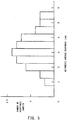
- FIG. 5 is a histogram showing the number of acceptable samples in the thermal cyclic test. It was found that, as shown in FIG. 5 , when a sample class value was 2 to 4 ⁇ m, the number of acceptable samples was not less than five. It is assumed that, when the sample class value is not less than 4.5 ⁇ m or the sample class value is not more than 1.5 ⁇ m, the total area where the tip and the electrode base material melt due to resistance welding became small, and strength against shearing force due to thermal expansion, of the electrode base material, which is generated in the thermal cyclic test decreases.
- rectangular plate-shaped electrode base materials each formed from a nickel-based alloy
- disc-shaped tips each having a diameter of 1 mm and a thickness of 0.4 mm
- Dry type polishing was performed on the front surface and the rear surface of each electrode base material by means of the polishing disc, so that a rectangular-shaped first surface and a rectangular-shaped second surface each having a length of 6 mm and a width of 2.7 mm were produced on the front surface and the rear surface, respectively, of the electrode base material.
- dry type polishing was performed on the front surface and the rear surface of each tip, so that a third surface and a fourth surface were produced on the front surface and the rear surface, respectively, of the tip.
- the arithmetic average roughness Ra of each of the first surface and the second surface of each electrode base material was measured (the measurement range was a rectangular range of 2.7 mm ⁇ 1 mm) by means of the laser microscope (VK-X110/X100), and the electrode base materials were classified into Samples 1 to 3 each having the first surface (surface on the tip side) and the second surface (surface on the first electrode side) both of which have various arithmetic average roughness.
- the sample class width was 0.5 ⁇ m, and each Sample contained 10 samples.
- a total of 30 tips were prepared in which the arithmetic average roughness of each of the third surface and the fourth surface was 0.45 to 0.8 ⁇ m.
- resistance welding was performed, by means of the resistance welding machine (power supply system was a single-phase AC system) used in Example 1, by applying current (target effective value of 1000 A) between the first electrode and the second electrode (the number of current application cycles was 7, and the number of slopes that are a rise of the applied current was 2) while applying a load of 330N in the thickness direction of the tip and the electrode base material.
- current target effective value of 1000 A
- the thermal cyclic test was performed as similar to that of Example 2, and, after the test, the polished cross-sectional surface including the central axis of the tip was produced.
- the polished cross-sectional surface was observed by means of the metallograph, and the length L of oxide scale (a portion from which the tip was separated) present between the electrode base material and the tip was measured.
- the Sample in which not less than five of the 10 samples had a value that exceeded 0.3, the value being obtained by dividing the length L(mm) by the diameter of the tip (1 mm), was evaluated as unacceptable.
- the Sample in which less than five of the 10 samples had a value that was not more than 0.3, was evaluated as acceptable.
- Sample class value ( ⁇ m) Results First surface Second surface Sample 1 2 4 Unacceptable Sample 2 3 3 Acceptable Sample 3 4 2 Acceptable
- Table 1 is a list of the test results. As indicated in Table 1, Samples 2 and 3, in which the arithmetic average roughness of the first surface (surface on the tip side) was not less than the arithmetic average roughness of the second surface (surface on the first electrode side), were evaluated as acceptable, and Sample 1, in which the arithmetic average roughness of the first surface was less than the arithmetic average roughness of the second surface, was evaluated as unacceptable. It is assumed that, since Samples 2 and 3 each had the arithmetic average roughness of the first surface that was not less than the arithmetic average roughness of the second surface, Samples 2 and 3 each ensured contact resistance between the first surface of the electrode base material and the tip. As a result, it is assumed that Joule heat during resistance welding was ensured and joining strength between the electrode base material and the tip was ensured, so that Samples 2 and 3 were evaluated as acceptable in the thermal cyclic test.
- Samples of the spark plug were manufactured as follows. Firstly, after the center electrode was inserted into the axial hole of the insulator, electrical connection was ensured between the metal terminal inserted into the axial hole and the center electrode. Next, the metal shell to which the electrode base material of the ground electrode was joined in advance was assembled to the outer circumference of the insulator. Next, after dry type polishing was performed on the electrode base material by means of a polishing brush, the tip on which dry type polishing was performed was joined to the electrode base material by means of resistance welding, so that 10 samples of the spark plug were obtained.
- rectangular-shaped electrode base materials each formed from a nickel-based alloy
- disc-shaped tips each having a diameter of 1 mm and a thickness of 0.4 mm
- dry type polishing a rectangular-shaped first surface and a rectangular-shaped second surface each having a length of 6 mm and a width of 2.7 mm were produced on the front surface and the rear surface, respectively, of each electrode base material.
- a third surface and a fourth surface were produced on the front surface and the rear surface, respectively, of each tip.
- the arithmetic average roughness of each of the first surface and the second surface measured (the measurement range was a rectangular range of 2.7 mm ⁇ 1 mm) by means of the laser microscope (VK-X110/X100) was 3 ⁇ m.
- the arithmetic average roughness of each of the third surface and the fourth surface, measured similarly, was 0.45 to 0.8 ⁇ m.
- Example 5 10 samples in Example 5 were manufactured as similar to Example 4, except that after the electrode base material of the ground electrode was joined to the metal shell, dry type polishing was performed on the electrode base material by means of the polishing brush, the metal shell was then assembled to the insulator, and resistance welding was performed on the tip and the electrode base material after the assembly.
- a notch was formed in the fourth surface (surface on the side opposite to the tip) of the electrode base material and the electrode base material was bent by 90 degrees, separation occurred between the tip and the electrode base material in four of the 10 samples.
- Example 4 and Example 5 are compared with each other, since the number of samples in which separation occurred was less in Example 4 than in Example 5, adhesion between the tip and the electrode base material was more stable in Example 4 than in Example 5. It is assumed that, since, in Example 5, polishing was performed on the electrode base material of the ground electrode before the metal shell was assembled to the insulator, foreign matter such as oxide film attached to the front surface of the electrode base material in the time period from the end of polishing to the start of resistance welding.
- Example 4 polishing was performed on the electrode base material of the ground electrode after the metal shell was assembled to the insulator, foreign matter such as oxide film is hardly generated on the front surface of the electrode base material in the time period from the end of polishing to the start of resistance welding. Accordingly, it is assumed that, in Example 4, variations in adhesion strength of the tip was suppressed.
- the present invention has been described based on the embodiments, the present invention is not limited to the above embodiments at all. It can be easily understood that various modifications can be devised without departing from the gist of the present invention.
- the shapes and the dimensions of the electrode base material 13 and the tip 14 are mere examples and may be set as appropriate.
- the resistance welding machine in which the power supply system is a single-phase AC system
- the resistance welding machine is not limited thereto.
- a power supply system such as a single-phase DC system, an inverter system, a capacitor system, and the like, may be set as appropriate.
- the present invention is not limited thereto.
- a pressing member (not shown) that presses, together with the second electrode 22, the electrode base material 13 and the tip 14 may be disposed on the straight line on which the second electrode 22 is located, and the first electrode 21 for current application, independently of the pressing member, may be provided to make contact with the electrode base material 13.
- the second surface may be produced at any position where the first electrode 21 makes contact with the electrode base material 13.
Landscapes
- Engineering & Computer Science (AREA)
- Manufacturing & Machinery (AREA)
- Spark Plugs (AREA)
Claims (3)
- Procédé de fabrication d'une bougie d'allumage (10) par la jonction d'une pointe (14) contenant un métal noble à un matériau de base d'électrode (13) au moyen d'un soudage par résistance dans lequel un courant est appliqué entre une première électrode (21) et une deuxième électrode (22), afin d'obtenir une électrode de masse (12), le procédé comprenant :une étape de réglage de matériau de base d'électrode comportant une première étape consistant à produire, sur le matériau de base d'électrode (13), une première surface (31) ayant une superficie supérieure ou égale à une superficie venant en contact avec la pointe (14), en effectuant au moins l'un parmi un polissage et un meulage sur le matériau de base d'électrode (13), et une deuxième étape consistant à produire, sur le matériau de base d'électrode (13), une deuxième surface (32) ayant une superficie supérieure ou égale à une superficie venant en contact avec la première électrode (21), en effectuant au moins l'un parmi un polissage et un meulage sur le matériau de base d'électrode (13) ; etune étape de soudage consistant à effectuer un soudage par résistance en appliquant un courant entre la première électrode (21) et la deuxième électrode (22), après avoir mis la première surface (31) du matériau de base d'électrode (13) et la pointe (14) en contact l'une avec l'autre, à mettre la première électrode (21) en contact avec la deuxième surface (32) du matériau de base d'électrode (13), et à mettre la deuxième électrode (22) en contact avec la pointe (14), dans lequelà l'étape de réglage de matériau de base d'électrode, une rugosité moyenne arithmétique de la première surface (31) est fixée pour ne pas être inférieure à une rugosité moyenne arithmétique de la deuxième surface (32),dans lequeldans le cas où une surface de la pointe (14), venant en contact avec le matériau de base d'électrode (13) est définie comme une troisième surface (33), et une surface de la pointe (14) venant en contact avec la deuxième électrode (22) est définie comme une quatrième surface (34),la rugosité moyenne arithmétique de chacune parmi la première surface (31) et la deuxième surface (32) du matériau de base d'électrode (13) est de 2 à 4 µm, et une rugosité moyenne arithmétique de chacune parmi la troisième surface (33) et la quatrième surface (34) de la pointe (14) est de 0,4 à 0,8 µm.
- Procédé de fabrication la bougie d'allumage (10) selon la revendication 1, comprenant en outre
une étape d'assemblage consistant à assembler une enveloppe métallique tubulaire (11), à laquelle le matériau de base d'électrode (13) est relié, à une circonférence extérieure d'un isolateur tubulaire (15), dans lequel
après l'étape d'assemblage, l'étape de réglage de matériau de base d'électrode est effectuée. - Procédé de fabrication la bougie d'allumage (10) selon la revendication 1, comprenant en outre :une troisième étape consistant à produire la troisième surface (33) sur la pointe (14) en effectuant au moins l'un parmi un polissage et un meulage sur celle-ci ; etune quatrième étape consistant à produire la quatrième surface (34) sur la pointe (14) en effectuant au moins l'un parmi un polissage et un meulage sur celle-ci.
Applications Claiming Priority (3)
| Application Number | Priority Date | Filing Date | Title |
|---|---|---|---|
| JP2016123876 | 2016-06-22 | ||
| JP2017059596A JP6166004B1 (ja) | 2016-06-22 | 2017-03-24 | スパークプラグの製造方法 |
| PCT/JP2017/016253 WO2017221541A1 (fr) | 2016-06-22 | 2017-04-25 | Procédé de production d'une bougie d'allumage |
Publications (3)
| Publication Number | Publication Date |
|---|---|
| EP3477800A1 EP3477800A1 (fr) | 2019-05-01 |
| EP3477800A4 EP3477800A4 (fr) | 2020-02-26 |
| EP3477800B1 true EP3477800B1 (fr) | 2020-11-18 |
Family
ID=59351401
Family Applications (1)
| Application Number | Title | Priority Date | Filing Date |
|---|---|---|---|
| EP17815012.4A Active EP3477800B1 (fr) | 2016-06-22 | 2017-04-25 | Procédé de production d'une bougie d'allumage |
Country Status (5)
| Country | Link |
|---|---|
| US (1) | US20190334323A1 (fr) |
| EP (1) | EP3477800B1 (fr) |
| JP (1) | JP6166004B1 (fr) |
| CN (1) | CN109417277B (fr) |
| WO (1) | WO2017221541A1 (fr) |
Families Citing this family (2)
| Publication number | Priority date | Publication date | Assignee | Title |
|---|---|---|---|---|
| JP6595546B2 (ja) * | 2017-09-06 | 2019-10-23 | 日本特殊陶業株式会社 | スパークプラグの製造方法 |
| JP7136915B2 (ja) * | 2018-10-31 | 2022-09-13 | 京セラ株式会社 | ヒータ |
Family Cites Families (5)
| Publication number | Priority date | Publication date | Assignee | Title |
|---|---|---|---|---|
| JP3269032B2 (ja) * | 1997-09-01 | 2002-03-25 | 日本特殊陶業株式会社 | スパークプラグ及びそれを用いた内燃機関用点火システム |
| JP2003123937A (ja) * | 2001-10-16 | 2003-04-25 | Denso Corp | スパークプラグおよびその製造方法 |
| JP4964281B2 (ja) * | 2009-09-11 | 2012-06-27 | 日本特殊陶業株式会社 | スパークプラグ |
| EP2667465B1 (fr) * | 2011-01-20 | 2019-11-20 | Ngk Spark Plug Co., Ltd. | Procédé de fabrication pour bougie d'allumage |
| JP6138712B2 (ja) * | 2014-02-19 | 2017-05-31 | 日本特殊陶業株式会社 | スパークプラグの製造方法 |
-
2017
- 2017-03-24 JP JP2017059596A patent/JP6166004B1/ja active Active
- 2017-04-25 CN CN201780038435.7A patent/CN109417277B/zh active Active
- 2017-04-25 EP EP17815012.4A patent/EP3477800B1/fr active Active
- 2017-04-25 WO PCT/JP2017/016253 patent/WO2017221541A1/fr not_active Ceased
- 2017-04-25 US US16/310,863 patent/US20190334323A1/en not_active Abandoned
Non-Patent Citations (1)
| Title |
|---|
| None * |
Also Published As
| Publication number | Publication date |
|---|---|
| CN109417277B (zh) | 2020-05-19 |
| EP3477800A1 (fr) | 2019-05-01 |
| JP6166004B1 (ja) | 2017-07-19 |
| JP2018006324A (ja) | 2018-01-11 |
| CN109417277A (zh) | 2019-03-01 |
| EP3477800A4 (fr) | 2020-02-26 |
| US20190334323A1 (en) | 2019-10-31 |
| WO2017221541A1 (fr) | 2017-12-28 |
Similar Documents
| Publication | Publication Date | Title |
|---|---|---|
| KR101019813B1 (ko) | 스파크 플러그 제조방법 및 스파크 플러그 | |
| EP2325959B1 (fr) | Bougie d allumage | |
| JP6795879B2 (ja) | 抵抗器及びその製造方法 | |
| JP6634927B2 (ja) | スパークプラグ及びスパークプラグの製造方法 | |
| JP5938392B2 (ja) | スパークプラグ | |
| KR101562151B1 (ko) | 점화 플러그용 클래드 전극 및 그 제조 방법 | |
| US6285106B1 (en) | Commutator | |
| EP3477800B1 (fr) | Procédé de production d'une bougie d'allumage | |
| JP6664320B2 (ja) | チップヒューズ及びその製造方法 | |
| Masomtob et al. | Parametric study of spot welding between Li-ion battery cells and sheet metal connectors | |
| KR101912502B1 (ko) | 스파크 플러그 및 그 제조 방법 | |
| EP2669724B1 (fr) | Connecteur pour fusion de fibres optiques | |
| JP2004158220A (ja) | スパークプラグ及びその製造方法 | |
| JP2009182144A (ja) | 抵抗器およびその製造方法 | |
| US20130277338A1 (en) | Resistance Welding Head with Parallel Electrodes | |
| KR101536085B1 (ko) | 스파크 플러그 | |
| JP6574738B2 (ja) | スパークプラグ | |
| EP2568548B1 (fr) | Procédé de fabrication d'une bougie d'allumage | |
| CN108788423A (zh) | 一种用于超薄板与小直径棒材之间t型连接的焊接装置 | |
| US3177560A (en) | Process for producing a thermistor | |
| JPH10112374A (ja) | スパークプラグおよびその製造方法 | |
| JPH07235363A (ja) | 内燃機関用スパークプラグの製造方法 | |
| WO2019049440A1 (fr) | Procédé de fabrication d'une bougie d'allumage | |
| US20190363521A1 (en) | Method for manufacturing spark plug | |
| JP2664742B2 (ja) | 電気接点の製造方法 |
Legal Events
| Date | Code | Title | Description |
|---|---|---|---|
| STAA | Information on the status of an ep patent application or granted ep patent |
Free format text: STATUS: THE INTERNATIONAL PUBLICATION HAS BEEN MADE |
|
| PUAI | Public reference made under article 153(3) epc to a published international application that has entered the european phase |
Free format text: ORIGINAL CODE: 0009012 |
|
| STAA | Information on the status of an ep patent application or granted ep patent |
Free format text: STATUS: REQUEST FOR EXAMINATION WAS MADE |
|
| 17P | Request for examination filed |
Effective date: 20181221 |
|
| AK | Designated contracting states |
Kind code of ref document: A1 Designated state(s): AL AT BE BG CH CY CZ DE DK EE ES FI FR GB GR HR HU IE IS IT LI LT LU LV MC MK MT NL NO PL PT RO RS SE SI SK SM TR |
|
| AX | Request for extension of the european patent |
Extension state: BA ME |
|
| DAV | Request for validation of the european patent (deleted) | ||
| DAX | Request for extension of the european patent (deleted) | ||
| RIN1 | Information on inventor provided before grant (corrected) |
Inventor name: SHIMAMURA, TAKUYA |
|
| REG | Reference to a national code |
Ref country code: DE Ref legal event code: R079 Ref document number: 602017027950 Country of ref document: DE Free format text: PREVIOUS MAIN CLASS: H01T0013200000 Ipc: H01T0021020000 |
|
| A4 | Supplementary search report drawn up and despatched |
Effective date: 20200123 |
|
| RIC1 | Information provided on ipc code assigned before grant |
Ipc: H01T 21/02 20060101AFI20200117BHEP Ipc: H01T 13/32 20060101ALI20200117BHEP |
|
| GRAP | Despatch of communication of intention to grant a patent |
Free format text: ORIGINAL CODE: EPIDOSNIGR1 |
|
| STAA | Information on the status of an ep patent application or granted ep patent |
Free format text: STATUS: GRANT OF PATENT IS INTENDED |
|
| INTG | Intention to grant announced |
Effective date: 20200803 |
|
| GRAS | Grant fee paid |
Free format text: ORIGINAL CODE: EPIDOSNIGR3 |
|
| GRAA | (expected) grant |
Free format text: ORIGINAL CODE: 0009210 |
|
| STAA | Information on the status of an ep patent application or granted ep patent |
Free format text: STATUS: THE PATENT HAS BEEN GRANTED |
|
| AK | Designated contracting states |
Kind code of ref document: B1 Designated state(s): AL AT BE BG CH CY CZ DE DK EE ES FI FR GB GR HR HU IE IS IT LI LT LU LV MC MK MT NL NO PL PT RO RS SE SI SK SM TR |
|
| REG | Reference to a national code |
Ref country code: GB Ref legal event code: FG4D |
|
| REG | Reference to a national code |
Ref country code: CH Ref legal event code: EP |
|
| REG | Reference to a national code |
Ref country code: IE Ref legal event code: FG4D |
|
| REG | Reference to a national code |
Ref country code: DE Ref legal event code: R096 Ref document number: 602017027950 Country of ref document: DE |
|
| REG | Reference to a national code |
Ref country code: AT Ref legal event code: REF Ref document number: 1336795 Country of ref document: AT Kind code of ref document: T Effective date: 20201215 |
|
| REG | Reference to a national code |
Ref country code: AT Ref legal event code: MK05 Ref document number: 1336795 Country of ref document: AT Kind code of ref document: T Effective date: 20201118 |
|
| REG | Reference to a national code |
Ref country code: NL Ref legal event code: MP Effective date: 20201118 |
|
| PG25 | Lapsed in a contracting state [announced via postgrant information from national office to epo] |
Ref country code: PT Free format text: LAPSE BECAUSE OF FAILURE TO SUBMIT A TRANSLATION OF THE DESCRIPTION OR TO PAY THE FEE WITHIN THE PRESCRIBED TIME-LIMIT Effective date: 20210318 Ref country code: RS Free format text: LAPSE BECAUSE OF FAILURE TO SUBMIT A TRANSLATION OF THE DESCRIPTION OR TO PAY THE FEE WITHIN THE PRESCRIBED TIME-LIMIT Effective date: 20201118 Ref country code: FI Free format text: LAPSE BECAUSE OF FAILURE TO SUBMIT A TRANSLATION OF THE DESCRIPTION OR TO PAY THE FEE WITHIN THE PRESCRIBED TIME-LIMIT Effective date: 20201118 Ref country code: NO Free format text: LAPSE BECAUSE OF FAILURE TO SUBMIT A TRANSLATION OF THE DESCRIPTION OR TO PAY THE FEE WITHIN THE PRESCRIBED TIME-LIMIT Effective date: 20210218 Ref country code: GR Free format text: LAPSE BECAUSE OF FAILURE TO SUBMIT A TRANSLATION OF THE DESCRIPTION OR TO PAY THE FEE WITHIN THE PRESCRIBED TIME-LIMIT Effective date: 20210219 |
|
| PG25 | Lapsed in a contracting state [announced via postgrant information from national office to epo] |
Ref country code: AT Free format text: LAPSE BECAUSE OF FAILURE TO SUBMIT A TRANSLATION OF THE DESCRIPTION OR TO PAY THE FEE WITHIN THE PRESCRIBED TIME-LIMIT Effective date: 20201118 Ref country code: BG Free format text: LAPSE BECAUSE OF FAILURE TO SUBMIT A TRANSLATION OF THE DESCRIPTION OR TO PAY THE FEE WITHIN THE PRESCRIBED TIME-LIMIT Effective date: 20210218 Ref country code: SE Free format text: LAPSE BECAUSE OF FAILURE TO SUBMIT A TRANSLATION OF THE DESCRIPTION OR TO PAY THE FEE WITHIN THE PRESCRIBED TIME-LIMIT Effective date: 20201118 Ref country code: LV Free format text: LAPSE BECAUSE OF FAILURE TO SUBMIT A TRANSLATION OF THE DESCRIPTION OR TO PAY THE FEE WITHIN THE PRESCRIBED TIME-LIMIT Effective date: 20201118 Ref country code: PL Free format text: LAPSE BECAUSE OF FAILURE TO SUBMIT A TRANSLATION OF THE DESCRIPTION OR TO PAY THE FEE WITHIN THE PRESCRIBED TIME-LIMIT Effective date: 20201118 Ref country code: IS Free format text: LAPSE BECAUSE OF FAILURE TO SUBMIT A TRANSLATION OF THE DESCRIPTION OR TO PAY THE FEE WITHIN THE PRESCRIBED TIME-LIMIT Effective date: 20210318 |
|
| REG | Reference to a national code |
Ref country code: LT Ref legal event code: MG9D |
|
| PG25 | Lapsed in a contracting state [announced via postgrant information from national office to epo] |
Ref country code: HR Free format text: LAPSE BECAUSE OF FAILURE TO SUBMIT A TRANSLATION OF THE DESCRIPTION OR TO PAY THE FEE WITHIN THE PRESCRIBED TIME-LIMIT Effective date: 20201118 |
|
| PG25 | Lapsed in a contracting state [announced via postgrant information from national office to epo] |
Ref country code: RO Free format text: LAPSE BECAUSE OF FAILURE TO SUBMIT A TRANSLATION OF THE DESCRIPTION OR TO PAY THE FEE WITHIN THE PRESCRIBED TIME-LIMIT Effective date: 20201118 Ref country code: SK Free format text: LAPSE BECAUSE OF FAILURE TO SUBMIT A TRANSLATION OF THE DESCRIPTION OR TO PAY THE FEE WITHIN THE PRESCRIBED TIME-LIMIT Effective date: 20201118 Ref country code: SM Free format text: LAPSE BECAUSE OF FAILURE TO SUBMIT A TRANSLATION OF THE DESCRIPTION OR TO PAY THE FEE WITHIN THE PRESCRIBED TIME-LIMIT Effective date: 20201118 Ref country code: EE Free format text: LAPSE BECAUSE OF FAILURE TO SUBMIT A TRANSLATION OF THE DESCRIPTION OR TO PAY THE FEE WITHIN THE PRESCRIBED TIME-LIMIT Effective date: 20201118 Ref country code: CZ Free format text: LAPSE BECAUSE OF FAILURE TO SUBMIT A TRANSLATION OF THE DESCRIPTION OR TO PAY THE FEE WITHIN THE PRESCRIBED TIME-LIMIT Effective date: 20201118 Ref country code: LT Free format text: LAPSE BECAUSE OF FAILURE TO SUBMIT A TRANSLATION OF THE DESCRIPTION OR TO PAY THE FEE WITHIN THE PRESCRIBED TIME-LIMIT Effective date: 20201118 |
|
| REG | Reference to a national code |
Ref country code: DE Ref legal event code: R097 Ref document number: 602017027950 Country of ref document: DE |
|
| PG25 | Lapsed in a contracting state [announced via postgrant information from national office to epo] |
Ref country code: DK Free format text: LAPSE BECAUSE OF FAILURE TO SUBMIT A TRANSLATION OF THE DESCRIPTION OR TO PAY THE FEE WITHIN THE PRESCRIBED TIME-LIMIT Effective date: 20201118 |
|
| PLBE | No opposition filed within time limit |
Free format text: ORIGINAL CODE: 0009261 |
|
| STAA | Information on the status of an ep patent application or granted ep patent |
Free format text: STATUS: NO OPPOSITION FILED WITHIN TIME LIMIT |
|
| 26N | No opposition filed |
Effective date: 20210819 |
|
| PG25 | Lapsed in a contracting state [announced via postgrant information from national office to epo] |
Ref country code: IT Free format text: LAPSE BECAUSE OF FAILURE TO SUBMIT A TRANSLATION OF THE DESCRIPTION OR TO PAY THE FEE WITHIN THE PRESCRIBED TIME-LIMIT Effective date: 20201118 Ref country code: NL Free format text: LAPSE BECAUSE OF FAILURE TO SUBMIT A TRANSLATION OF THE DESCRIPTION OR TO PAY THE FEE WITHIN THE PRESCRIBED TIME-LIMIT Effective date: 20201118 Ref country code: AL Free format text: LAPSE BECAUSE OF FAILURE TO SUBMIT A TRANSLATION OF THE DESCRIPTION OR TO PAY THE FEE WITHIN THE PRESCRIBED TIME-LIMIT Effective date: 20201118 |
|
| PG25 | Lapsed in a contracting state [announced via postgrant information from national office to epo] |
Ref country code: MC Free format text: LAPSE BECAUSE OF FAILURE TO SUBMIT A TRANSLATION OF THE DESCRIPTION OR TO PAY THE FEE WITHIN THE PRESCRIBED TIME-LIMIT Effective date: 20201118 Ref country code: SI Free format text: LAPSE BECAUSE OF FAILURE TO SUBMIT A TRANSLATION OF THE DESCRIPTION OR TO PAY THE FEE WITHIN THE PRESCRIBED TIME-LIMIT Effective date: 20201118 |
|
| GBPC | Gb: european patent ceased through non-payment of renewal fee |
Effective date: 20210425 |
|
| PG25 | Lapsed in a contracting state [announced via postgrant information from national office to epo] |
Ref country code: LU Free format text: LAPSE BECAUSE OF NON-PAYMENT OF DUE FEES Effective date: 20210425 |
|
| REG | Reference to a national code |
Ref country code: BE Ref legal event code: MM Effective date: 20210430 |
|
| PG25 | Lapsed in a contracting state [announced via postgrant information from national office to epo] |
Ref country code: LI Free format text: LAPSE BECAUSE OF NON-PAYMENT OF DUE FEES Effective date: 20210430 Ref country code: CH Free format text: LAPSE BECAUSE OF NON-PAYMENT OF DUE FEES Effective date: 20210430 Ref country code: FR Free format text: LAPSE BECAUSE OF NON-PAYMENT OF DUE FEES Effective date: 20210430 Ref country code: GB Free format text: LAPSE BECAUSE OF NON-PAYMENT OF DUE FEES Effective date: 20210425 Ref country code: ES Free format text: LAPSE BECAUSE OF FAILURE TO SUBMIT A TRANSLATION OF THE DESCRIPTION OR TO PAY THE FEE WITHIN THE PRESCRIBED TIME-LIMIT Effective date: 20201118 |
|
| PG25 | Lapsed in a contracting state [announced via postgrant information from national office to epo] |
Ref country code: IE Free format text: LAPSE BECAUSE OF NON-PAYMENT OF DUE FEES Effective date: 20210425 |
|
| PG25 | Lapsed in a contracting state [announced via postgrant information from national office to epo] |
Ref country code: IS Free format text: LAPSE BECAUSE OF FAILURE TO SUBMIT A TRANSLATION OF THE DESCRIPTION OR TO PAY THE FEE WITHIN THE PRESCRIBED TIME-LIMIT Effective date: 20210318 |
|
| PG25 | Lapsed in a contracting state [announced via postgrant information from national office to epo] |
Ref country code: BE Free format text: LAPSE BECAUSE OF NON-PAYMENT OF DUE FEES Effective date: 20210430 |
|
| P01 | Opt-out of the competence of the unified patent court (upc) registered |
Effective date: 20230512 |
|
| PG25 | Lapsed in a contracting state [announced via postgrant information from national office to epo] |
Ref country code: CY Free format text: LAPSE BECAUSE OF FAILURE TO SUBMIT A TRANSLATION OF THE DESCRIPTION OR TO PAY THE FEE WITHIN THE PRESCRIBED TIME-LIMIT Effective date: 20201118 |
|
| PG25 | Lapsed in a contracting state [announced via postgrant information from national office to epo] |
Ref country code: HU Free format text: LAPSE BECAUSE OF FAILURE TO SUBMIT A TRANSLATION OF THE DESCRIPTION OR TO PAY THE FEE WITHIN THE PRESCRIBED TIME-LIMIT; INVALID AB INITIO Effective date: 20170425 |
|
| REG | Reference to a national code |
Ref country code: DE Ref legal event code: R081 Ref document number: 602017027950 Country of ref document: DE Owner name: NITERRA CO., LTD., NAGOYA-SHI, JP Free format text: FORMER OWNER: NGK SPARK PLUG CO., LTD., NAGOYA-SHI, AICHI, JP |
|
| PG25 | Lapsed in a contracting state [announced via postgrant information from national office to epo] |
Ref country code: MK Free format text: LAPSE BECAUSE OF FAILURE TO SUBMIT A TRANSLATION OF THE DESCRIPTION OR TO PAY THE FEE WITHIN THE PRESCRIBED TIME-LIMIT Effective date: 20201118 |
|
| PG25 | Lapsed in a contracting state [announced via postgrant information from national office to epo] |
Ref country code: TR Free format text: LAPSE BECAUSE OF FAILURE TO SUBMIT A TRANSLATION OF THE DESCRIPTION OR TO PAY THE FEE WITHIN THE PRESCRIBED TIME-LIMIT Effective date: 20201118 |
|
| PG25 | Lapsed in a contracting state [announced via postgrant information from national office to epo] |
Ref country code: MT Free format text: LAPSE BECAUSE OF FAILURE TO SUBMIT A TRANSLATION OF THE DESCRIPTION OR TO PAY THE FEE WITHIN THE PRESCRIBED TIME-LIMIT Effective date: 20201118 |
|
| PGFP | Annual fee paid to national office [announced via postgrant information from national office to epo] |
Ref country code: DE Payment date: 20250305 Year of fee payment: 9 |