EP3479409B1 - Optoelektronische vorrichtung mit dreidimensionalen dioden - Google Patents
Optoelektronische vorrichtung mit dreidimensionalen dioden Download PDFInfo
- Publication number
- EP3479409B1 EP3479409B1 EP17742491.8A EP17742491A EP3479409B1 EP 3479409 B1 EP3479409 B1 EP 3479409B1 EP 17742491 A EP17742491 A EP 17742491A EP 3479409 B1 EP3479409 B1 EP 3479409B1
- Authority
- EP
- European Patent Office
- Prior art keywords
- nucleation
- diodes
- conductive
- optoelectronic device
- insulating layer
- Prior art date
- Legal status (The legal status is an assumption and is not a legal conclusion. Google has not performed a legal analysis and makes no representation as to the accuracy of the status listed.)
- Active
Links
Images


Classifications
-
- H—ELECTRICITY
- H10—SEMICONDUCTOR DEVICES; ELECTRIC SOLID-STATE DEVICES NOT OTHERWISE PROVIDED FOR
- H10H—INORGANIC LIGHT-EMITTING SEMICONDUCTOR DEVICES HAVING POTENTIAL BARRIERS
- H10H29/00—Integrated devices, or assemblies of multiple devices, comprising at least one light-emitting semiconductor element covered by group H10H20/00
- H10H29/10—Integrated devices comprising at least one light-emitting semiconductor component covered by group H10H20/00
- H10H29/14—Integrated devices comprising at least one light-emitting semiconductor component covered by group H10H20/00 comprising multiple light-emitting semiconductor components
- H10H29/142—Two-dimensional arrangements, e.g. asymmetric LED layout
-
- H—ELECTRICITY
- H10—SEMICONDUCTOR DEVICES; ELECTRIC SOLID-STATE DEVICES NOT OTHERWISE PROVIDED FOR
- H10H—INORGANIC LIGHT-EMITTING SEMICONDUCTOR DEVICES HAVING POTENTIAL BARRIERS
- H10H20/00—Individual inorganic light-emitting semiconductor devices having potential barriers, e.g. light-emitting diodes [LED]
- H10H20/01—Manufacture or treatment
- H10H20/011—Manufacture or treatment of bodies, e.g. forming semiconductor layers
- H10H20/013—Manufacture or treatment of bodies, e.g. forming semiconductor layers having light-emitting regions comprising only Group III-V materials
- H10H20/0133—Manufacture or treatment of bodies, e.g. forming semiconductor layers having light-emitting regions comprising only Group III-V materials with a substrate not being Group III-V materials
- H10H20/01335—Manufacture or treatment of bodies, e.g. forming semiconductor layers having light-emitting regions comprising only Group III-V materials with a substrate not being Group III-V materials the light-emitting regions comprising nitride materials
-
- H—ELECTRICITY
- H10—SEMICONDUCTOR DEVICES; ELECTRIC SOLID-STATE DEVICES NOT OTHERWISE PROVIDED FOR
- H10F—INORGANIC SEMICONDUCTOR DEVICES SENSITIVE TO INFRARED RADIATION, LIGHT, ELECTROMAGNETIC RADIATION OF SHORTER WAVELENGTH OR CORPUSCULAR RADIATION
- H10F39/00—Integrated devices, or assemblies of multiple devices, comprising at least one element covered by group H10F30/00, e.g. radiation detectors comprising photodiode arrays
- H10F39/10—Integrated devices
- H10F39/107—Integrated devices having multiple elements covered by H10F30/00 in a repetitive configuration, e.g. radiation detectors comprising photodiode arrays
-
- H—ELECTRICITY
- H10—SEMICONDUCTOR DEVICES; ELECTRIC SOLID-STATE DEVICES NOT OTHERWISE PROVIDED FOR
- H10F—INORGANIC SEMICONDUCTOR DEVICES SENSITIVE TO INFRARED RADIATION, LIGHT, ELECTROMAGNETIC RADIATION OF SHORTER WAVELENGTH OR CORPUSCULAR RADIATION
- H10F71/00—Manufacture or treatment of devices covered by this subclass
- H10F71/127—The active layers comprising only Group III-V materials, e.g. GaAs or InP
- H10F71/1276—The active layers comprising only Group III-V materials, e.g. GaAs or InP comprising growth substrates not made of Group III-V materials
-
- H—ELECTRICITY
- H10—SEMICONDUCTOR DEVICES; ELECTRIC SOLID-STATE DEVICES NOT OTHERWISE PROVIDED FOR
- H10F—INORGANIC SEMICONDUCTOR DEVICES SENSITIVE TO INFRARED RADIATION, LIGHT, ELECTROMAGNETIC RADIATION OF SHORTER WAVELENGTH OR CORPUSCULAR RADIATION
- H10F71/00—Manufacture or treatment of devices covered by this subclass
- H10F71/127—The active layers comprising only Group III-V materials, e.g. GaAs or InP
- H10F71/1278—The active layers comprising only Group III-V materials, e.g. GaAs or InP comprising nitrides, e.g. GaN
-
- H—ELECTRICITY
- H10—SEMICONDUCTOR DEVICES; ELECTRIC SOLID-STATE DEVICES NOT OTHERWISE PROVIDED FOR
- H10F—INORGANIC SEMICONDUCTOR DEVICES SENSITIVE TO INFRARED RADIATION, LIGHT, ELECTROMAGNETIC RADIATION OF SHORTER WAVELENGTH OR CORPUSCULAR RADIATION
- H10F77/00—Constructional details of devices covered by this subclass
- H10F77/10—Semiconductor bodies
- H10F77/12—Active materials
- H10F77/124—Active materials comprising only Group III-V materials, e.g. GaAs
- H10F77/1246—III-V nitrides, e.g. GaN
-
- H—ELECTRICITY
- H10—SEMICONDUCTOR DEVICES; ELECTRIC SOLID-STATE DEVICES NOT OTHERWISE PROVIDED FOR
- H10F—INORGANIC SEMICONDUCTOR DEVICES SENSITIVE TO INFRARED RADIATION, LIGHT, ELECTROMAGNETIC RADIATION OF SHORTER WAVELENGTH OR CORPUSCULAR RADIATION
- H10F77/00—Constructional details of devices covered by this subclass
- H10F77/10—Semiconductor bodies
- H10F77/14—Shape of semiconductor bodies; Shapes, relative sizes or dispositions of semiconductor regions within semiconductor bodies
- H10F77/147—Shapes of bodies
-
- H—ELECTRICITY
- H10—SEMICONDUCTOR DEVICES; ELECTRIC SOLID-STATE DEVICES NOT OTHERWISE PROVIDED FOR
- H10F—INORGANIC SEMICONDUCTOR DEVICES SENSITIVE TO INFRARED RADIATION, LIGHT, ELECTROMAGNETIC RADIATION OF SHORTER WAVELENGTH OR CORPUSCULAR RADIATION
- H10F77/00—Constructional details of devices covered by this subclass
- H10F77/20—Electrodes
- H10F77/206—Electrodes for devices having potential barriers
-
- H—ELECTRICITY
- H10—SEMICONDUCTOR DEVICES; ELECTRIC SOLID-STATE DEVICES NOT OTHERWISE PROVIDED FOR
- H10F—INORGANIC SEMICONDUCTOR DEVICES SENSITIVE TO INFRARED RADIATION, LIGHT, ELECTROMAGNETIC RADIATION OF SHORTER WAVELENGTH OR CORPUSCULAR RADIATION
- H10F77/00—Constructional details of devices covered by this subclass
- H10F77/40—Optical elements or arrangements
- H10F77/413—Optical elements or arrangements directly associated or integrated with the devices, e.g. back reflectors
-
- H—ELECTRICITY
- H10—SEMICONDUCTOR DEVICES; ELECTRIC SOLID-STATE DEVICES NOT OTHERWISE PROVIDED FOR
- H10F—INORGANIC SEMICONDUCTOR DEVICES SENSITIVE TO INFRARED RADIATION, LIGHT, ELECTROMAGNETIC RADIATION OF SHORTER WAVELENGTH OR CORPUSCULAR RADIATION
- H10F77/00—Constructional details of devices covered by this subclass
- H10F77/93—Interconnections
- H10F77/933—Interconnections for devices having potential barriers
-
- H—ELECTRICITY
- H10—SEMICONDUCTOR DEVICES; ELECTRIC SOLID-STATE DEVICES NOT OTHERWISE PROVIDED FOR
- H10H—INORGANIC LIGHT-EMITTING SEMICONDUCTOR DEVICES HAVING POTENTIAL BARRIERS
- H10H20/00—Individual inorganic light-emitting semiconductor devices having potential barriers, e.g. light-emitting diodes [LED]
- H10H20/80—Constructional details
- H10H20/81—Bodies
- H10H20/817—Bodies characterised by the crystal structures or orientations, e.g. polycrystalline, amorphous or porous
- H10H20/818—Bodies characterised by the crystal structures or orientations, e.g. polycrystalline, amorphous or porous within the light-emitting regions
-
- H—ELECTRICITY
- H10—SEMICONDUCTOR DEVICES; ELECTRIC SOLID-STATE DEVICES NOT OTHERWISE PROVIDED FOR
- H10H—INORGANIC LIGHT-EMITTING SEMICONDUCTOR DEVICES HAVING POTENTIAL BARRIERS
- H10H20/00—Individual inorganic light-emitting semiconductor devices having potential barriers, e.g. light-emitting diodes [LED]
- H10H20/80—Constructional details
- H10H20/81—Bodies
- H10H20/819—Bodies characterised by their shape, e.g. curved or truncated substrates
- H10H20/821—Bodies characterised by their shape, e.g. curved or truncated substrates of the light-emitting regions, e.g. non-planar junctions
-
- H—ELECTRICITY
- H10—SEMICONDUCTOR DEVICES; ELECTRIC SOLID-STATE DEVICES NOT OTHERWISE PROVIDED FOR
- H10H—INORGANIC LIGHT-EMITTING SEMICONDUCTOR DEVICES HAVING POTENTIAL BARRIERS
- H10H20/00—Individual inorganic light-emitting semiconductor devices having potential barriers, e.g. light-emitting diodes [LED]
- H10H20/80—Constructional details
- H10H20/81—Bodies
- H10H20/822—Materials of the light-emitting regions
- H10H20/824—Materials of the light-emitting regions comprising only Group III-V materials, e.g. GaP
- H10H20/825—Materials of the light-emitting regions comprising only Group III-V materials, e.g. GaP containing nitrogen, e.g. GaN
-
- H—ELECTRICITY
- H10—SEMICONDUCTOR DEVICES; ELECTRIC SOLID-STATE DEVICES NOT OTHERWISE PROVIDED FOR
- H10H—INORGANIC LIGHT-EMITTING SEMICONDUCTOR DEVICES HAVING POTENTIAL BARRIERS
- H10H20/00—Individual inorganic light-emitting semiconductor devices having potential barriers, e.g. light-emitting diodes [LED]
- H10H20/80—Constructional details
- H10H20/83—Electrodes
- H10H20/831—Electrodes characterised by their shape
- H10H20/8314—Electrodes characterised by their shape extending at least partially onto an outer side surface of the bodies
-
- H—ELECTRICITY
- H10—SEMICONDUCTOR DEVICES; ELECTRIC SOLID-STATE DEVICES NOT OTHERWISE PROVIDED FOR
- H10H—INORGANIC LIGHT-EMITTING SEMICONDUCTOR DEVICES HAVING POTENTIAL BARRIERS
- H10H20/00—Individual inorganic light-emitting semiconductor devices having potential barriers, e.g. light-emitting diodes [LED]
- H10H20/80—Constructional details
- H10H20/83—Electrodes
- H10H20/832—Electrodes characterised by their material
- H10H20/833—Transparent materials
-
- H—ELECTRICITY
- H10—SEMICONDUCTOR DEVICES; ELECTRIC SOLID-STATE DEVICES NOT OTHERWISE PROVIDED FOR
- H10H—INORGANIC LIGHT-EMITTING SEMICONDUCTOR DEVICES HAVING POTENTIAL BARRIERS
- H10H20/00—Individual inorganic light-emitting semiconductor devices having potential barriers, e.g. light-emitting diodes [LED]
- H10H20/80—Constructional details
- H10H20/84—Coatings, e.g. passivation layers or antireflective coatings
- H10H20/841—Reflective coatings, e.g. dielectric Bragg reflectors
-
- H—ELECTRICITY
- H10—SEMICONDUCTOR DEVICES; ELECTRIC SOLID-STATE DEVICES NOT OTHERWISE PROVIDED FOR
- H10H—INORGANIC LIGHT-EMITTING SEMICONDUCTOR DEVICES HAVING POTENTIAL BARRIERS
- H10H20/00—Individual inorganic light-emitting semiconductor devices having potential barriers, e.g. light-emitting diodes [LED]
- H10H20/80—Constructional details
- H10H20/85—Packages
- H10H20/857—Interconnections, e.g. lead-frames, bond wires or solder balls
-
- H—ELECTRICITY
- H10—SEMICONDUCTOR DEVICES; ELECTRIC SOLID-STATE DEVICES NOT OTHERWISE PROVIDED FOR
- H10F—INORGANIC SEMICONDUCTOR DEVICES SENSITIVE TO INFRARED RADIATION, LIGHT, ELECTROMAGNETIC RADIATION OF SHORTER WAVELENGTH OR CORPUSCULAR RADIATION
- H10F77/00—Constructional details of devices covered by this subclass
- H10F77/10—Semiconductor bodies
- H10F77/14—Shape of semiconductor bodies; Shapes, relative sizes or dispositions of semiconductor regions within semiconductor bodies
- H10F77/143—Shape of semiconductor bodies; Shapes, relative sizes or dispositions of semiconductor regions within semiconductor bodies comprising quantum structures
- H10F77/1437—Quantum wires or nanorods
-
- H—ELECTRICITY
- H10—SEMICONDUCTOR DEVICES; ELECTRIC SOLID-STATE DEVICES NOT OTHERWISE PROVIDED FOR
- H10H—INORGANIC LIGHT-EMITTING SEMICONDUCTOR DEVICES HAVING POTENTIAL BARRIERS
- H10H20/00—Individual inorganic light-emitting semiconductor devices having potential barriers, e.g. light-emitting diodes [LED]
- H10H20/80—Constructional details
- H10H20/81—Bodies
- H10H20/811—Bodies having quantum effect structures or superlattices, e.g. tunnel junctions
- H10H20/812—Bodies having quantum effect structures or superlattices, e.g. tunnel junctions within the light-emitting regions, e.g. having quantum confinement structures
Definitions
- the field of the invention is that of optoelectronic devices with light-emitting diodes or photodiodes.
- the invention applies to the field of light-emitting diode array devices such as lighting devices, display screens and image projectors, as well as to the field of photodiode array devices such as photodetectors. and sensors.
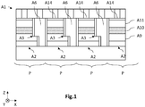
- this optoelectronic device A1 comprises a plurality of light-emitting diodes A2 each comprising a stack of a p-doped portion A11 and of an n-doped portion A9 separated from each other by an active zone A10 from which is mainly generated the light radiation from diode A2.
- the light-emitting diodes A2 have a so-called mesa structure, that is to say they are obtained from a stack of semiconductor layers intended to form the portions A9, A11 doped n and p as well as the active zone A10, a localized etching being carried out so as to individualize the light-emitting diodes A2 from one another.
- Each diode A2 has an L-shape, the sides of which are coated with an insulating layer, except at the level of a step A3 formed by the n-doped portion A9.
- First electrodes A14 rest on the upper surface of the p-doped portions A11 and second electrodes A6 extend between the diodes A2 and come into contact with the cutouts A3 formed by the n-doped portions A9.
- a display pixel then comprises the stack of doped portions A9, A11, of the active zone A10, and of the first electrode A14, as well as the second electrode A6 adjacent to the stack.
- a connection structure is assembled on the upper face of the matrix of light-emitting diodes and is intended to be hybridized to an integrated control circuit.
- This optoelectronic device however has the drawback of requiring an etching step of the doped semiconductor layers and of the active layer in order to individualize the diodes. Now, this etching step can lead to the formation of structural defects liable to degrade the optical and / or electronic properties of the diodes.
- the ratio between the emissive area of each diode on the area of each pixel is reduced by the need to form a step in the n-doped portion and by the presence of the second electrode which extends between the diodes so as to come into contact with this recess. This thus reduces the maximum light intensity relative to each pixel.
- the document WO2014 / 064276 describes a method of manufacturing an optoelectronic device comprising epitaxial wire diodes from nucleation pads which rest on a substrate and are separated from each other by a dielectric zone extending in the substrate.
- WO2014 / 056762 describes a method of manufacturing an optoelectronic device comprising the elimination of the growth substrate and the elimination of an upper part of the diodes to then allow them to be electrically polarized by means of conductive strips.
- the document US2013 / 112944 describes an optoelectronic device comprising a plurality of wire diodes arranged in distinct pixels, the wire diodes of the same pixel being covered with a conductive layer.
- the support may comprise an electrically insulating substrate, an upper face of which forms said front face, or may comprise a layer or a substrate, semiconductor or electrically conductor, coated with a so-called lower insulating layer, one face of which forms said front face.
- Each nucleation conductive strip can extend longitudinally on the front face, being electrically separated from its neighbors, transversely, by said intermediate insulating layer.
- Each upper conductive strip can extend longitudinally over the intermediate insulating layer, being electrically separated from its neighbors, transversely, by a so-called upper insulating layer.
- the upper conductive strips may be of an at least partially transparent conductive material, and may at least partially cover the second doped portions.
- Each upper conductive strip may include parts covering the second doped portions of a set of diodes, said so-called covering parts being connected to one another by so-called connecting parts resting on the intermediate insulating layer.
- the connecting parts of the upper conductive strips can be coated at least in part with a metal layer.
- the optoelectronic device may include first connection pads resting on said rear face, and electrically connected to the conductive nucleation strips by first orifices passing through the support and filled with a conductive material, and / or may include second connection pads resting on said rear face, and electrically connected to the upper conductive strips by second orifices passing through the support and the intermediate insulating layer and filled with a conductive material.
- the optoelectronic device may comprise an integrated control circuit assembled to the support and electrically connected to the nucleation conductive strips and to the upper conductive strips, adapted to apply a potential difference, sequentially, to different subsets of diodes, the diode or diodes of 'a same subset being in contact with the same nucleation conductive strip and with the same upper conductive strip, the diode (s) of different diode subsets being in contact with different nucleation conductive strips and / or of different upper conductive bands.
- At least one diode in contact with a first conductive nucleation strip and a first upper conductive strip may be connected in series with at least another diode, the latter being in contact with a second conductive nucleation strip distinct from the first nucleation strip and a second upper conductive strip distinct from the first upper strip.
- the support can be formed from a substrate made of a monocrystalline material forming an upper surface, on which rests a so-called lower insulating layer made of a dielectric material, epitaxied from the upper surface of the substrate and forming an opposite upper surface, the conductive strips nucleation being in a material comprising a transition metal forming a crystalline nucleating material, epitaxied from the upper surface of the lower insulating layer and forming a nucleation surface on which the first doped portions of said diodes are in contact.
- the material of the lower insulating layer can be chosen from aluminum nitride and oxides of aluminum, titanium, hafnium, magnesium and zirconium, and has a hexagonal, face-centered cubic or orthorhombic crystal structure.
- the material of the nucleation conductive bands can be chosen from titanium, vanadium, chromium, zirconium, niobium, molybdenum, hafnium, tantalum and tungsten, or from a nitride or a carbide of titanium or vanadium , chromium, zirconium, niobium, molybdenum, hafnium, tantalum and tungsten, and exhibits a face-centered hexagonal or cubic crystal structure. It may as a variant be a material based on gallium nitride, for example GaN, AIGaN, InGaN, or AlInGaN.
- the monocrystalline material of the substrate can be chosen from a III-V compound, a II-VI compound, or an element or compound IV, and has a face-centered hexagonal or cubic crystal structure.
- the invention also relates to a method for producing the optoelectronic device according to any one of the preceding characteristics, comprising a step of epitaxial growth of the conductive bands of nucleation by cathodic sputtering at a growth temperature between room temperature and 500 ° C. .
- an optoelectronic device with diodes for example light emitting diodes having a three-dimensional shape which each have a first doped portion and a second doped portion arranged to form a p-n junction.
- the diodes can be light emitting diodes adapted to emit light radiation or be photodiodes adapted to receive light radiation.
- the three-dimensional shape of the diodes may be such that the diodes have a wire shape, a pad shape, a pyramidal shape or the like.
- the first doped portions of the diodes extend along a longitudinal axis substantially orthogonal to the main plane of the support.
- the optoelectronic device comprises first electrodes adapted to bring the first doped portions of the diodes to a first electric potential V1, and second electrodes adapted to bring the second doped portions to a second electric potential V2.
- the first electrodes are in the form of conductive nucleation bands, distinct from one another, on which the first doped portions rest and are in contact.
- the second electrodes are in the form of so-called upper conductive strips, distinct from each other, in contact with the second doped portions.
- a three-dimensional direct coordinate system (X, Y, Z), where the X and Y axes form a plane parallel to the main plane of the substrate, and where the Z axis is oriented in a substantially orthogonal manner to the growing side of the substrate.
- the terms “vertical” and “vertically” are understood to relate to an orientation substantially parallel to the Z axis
- the terms “lower” and “upper” are understood to relate to an increasing positioning when one moves away from the growth face of the substrate in the + Z direction.
- conductive strip is meant an area of a semiconductor or conductive material, deposited in a thin layer, which has a longitudinal dimension in the plane (X, Y), or length, greater than the transverse dimension in the plane (X, Y ), or width, and the thickness dimension along the Z axis.
- Each conductive nucleation strip of index i is in contact with a set D i of several diodes which are in contact with different upper conductive strips.
- each upper conductive strip of index j is in contact with a set D j of several diodes which are in contact with different conductive nucleation strips.
- the diode (s) which are in contact with the same conductive nucleation strip of index i and of the same upper conductive strip of index j form a pixel P of indices i, j.
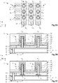
- FIGS. 2A, 2B and 2C are schematic and partial views, respectively in top view, in cross section along plane AA and along plane BB, of an optoelectronic device 1 with light-emitting diodes 2 according to a first embodiment.
- each pixel P ij comprises a single diode, but it may alternatively comprise a plurality of diodes.
- each nucleation conductive strip 6 i is in contact with a set D i of diodes, distributed into subsets P ij distinct from one another.
- Each subset P ij of diodes of the same nucleation conductive strip 6 i is in contact with the same upper conductive strip 14 of index j and form a pixel P ij .
- the support 3 has two faces, called front 3b and rear 3a, opposite to each other. It can be a one-piece structure, or be formed from a stack of layers such as a substrate 4 of the SOI type (for Silicon On Insulator, in English). It comprises an electrically insulating material at the level of the front face 3b. It can thus be formed, for example, of a one-piece insulating substrate 4, or be formed of a semiconductor or conductive substrate 4, the upper face of which is coated with an insulating layer 5.
- the material of the substrate 4 can be electrically insulating, such as for example a silicon oxide (for example SiO2) or sapphire, or be a semiconductor material for example chosen from III-V compounds comprising at least one element from column III and at least one element from column V of the periodic table, compounds II-VI or elements or compounds IV.
- a silicon oxide for example SiO2
- a semiconductor material for example chosen from III-V compounds comprising at least one element from column III and at least one element from column V of the periodic table, compounds II-VI or elements or compounds IV.
- it can be silicon, germanium, silicon carbide.
- the semiconductor material of the substrate 4 is monocrystalline silicon.
- the substrate 4 can have a thickness of between 50 nm and 1500 ⁇ m, depending on whether it has been thinned or not.
- the support has been thinned in order to allow electrical contact to be taken up on the rear face 3a
- it has a thickness for example between 10 ⁇ m and 300 ⁇ m, preferably between 10 ⁇ m and 100 ⁇ m.
- it has a thickness of between 300 ⁇ m and 1500 ⁇ m, for example equal to approximately 725 ⁇ m.
- the support is formed from a semiconductor substrate 4, the upper face of which is coated with a so-called lower insulating layer 5 made of a dielectric material.
- the lower insulating layer 5 provides electrical insulation between the conductive nucleation strips 6 i and the substrate 4 when the latter is electrically conductive.
- the material of the lower insulating layer 5 can be a silicon oxide (for example SiO2) or aluminum (for example Al2O3), a silicon nitride SiNx or aluminum AIN, a silicon oxynitride SiOxNy, or any other material. adapted.
- the thickness of the lower insulating layer 5 may be between 5 nm and 500 nm, preferably between 10 nm and 100 nm, for example equal to approximately 30 nm.
- the substrate can be omitted and the support can then be formed from a deposited layer, for example a reflective layer, possibly metallic, allowing the reflection of the incident light radiation. emitted by the diodes 2.
- the steps of removing the substrate and depositing the layer of the support can be carried out after the diodes have been produced.
- the first polarization electrodes are arranged so as to allow the application of a first electric potential V1 i to different sets of diodes. They take the form of a plurality of nucleation conductive strips 6 i which rest on the front face 3b of the support, here the upper face of the lower insulating layer 5. Each nucleation conductive strip 6 i has an upper face, opposite to the front face 3b of the support, which forms a nucleation surface on which each first doped portion 9 of diode 2 is in contact.
- the nucleation conductive bands 6 i are distinct from one another and may have an electric potential V1 i which varies over time, the value of which may be different from one band to another.
- Each conductive nucleation strip 6 of index i is in contact with a set D i of diodes at the level of the first doped portions 9 thereof, the sets of diodes being different from a conductive nucleation strip 6 i to l 'other.
- the nucleation conductive bands 6 i are made of an electrically conductive material suitable for the nucleation and the growth of the first doped portions 9.
- This material may be gallium nitride GaN, or an alloy based on gallium nitride, for example gallium and aluminum nitride AlGaN, gallium and indium nitride InGaN, or even gallium, aluminum and indium nitride AlInGaN.
- the nucleation conductive bands 6 i can alternatively be made of a material comprising a transition metal.
- It can be chosen from titanium, vanadium, chromium, zirconium, niobium, molybdenum, hafnium, tantalum and tungsten, or from a nitride or a transition metal carbide, for example of titanium, of zirconium, hafnium, vanadium, niobium, tantalum, chromium, molybdenum, tantalum, or a combination of these compounds.
- the transition metals, as well as their nitrides and carbides, have the advantages of allowing the nucleation of the first doped portions 9 and of having an electrical conductivity close to that of the metals.
- the nucleation conductive strips 6 i have a thickness for example between 5 nm and 500 nm, preferably between 10 nm and 100 nm, for example equal to approximately 30 nm. They have a transverse dimension in the plane (X, Y), or width, for example between 20 nm and 50 ⁇ m, preferably between 200 nm and 10 ⁇ m, preferably between 800 nm and 5 ⁇ m, for example equal to approximately 1 ⁇ m.
- the nucleation conductive bands 6 i are spaced transversely from one another by a distance for example between 500 nm and 20 ⁇ m, preferably between 1000 nm and 2000 nm, for example equal to 1500 nm.
- the optoelectronic device 1 further comprises a so-called intermediate insulating layer 7 which covers the front face 3b of the support, and in particular covers the conductive nucleation bands 6 i . It forms a growth mask allowing epitaxial growth of the first doped portions 9 of the diodes from through openings 8 opening locally on the nucleation surfaces. In addition, it extends so as to separate each conductive nucleation strip 6 i , transversely, from its neighbors. It also participates in ensuring the electrical insulation between the nucleation conductive bands 6 i and the upper conductive bands 14 j .
- the intermediate insulating layer 7 is made of one or more dielectric materials such as, for example, a silicon oxide (for example SiO2) or a silicon nitride (for example Si3N4 or SiN), or even a silicon oxynitride, an oxide of silicon. aluminum (eg Al2O3) or an oxide of hafnium (eg HfO2).
- the thickness of the intermediate insulating layer 7 may be between 5 nm and 500 nm, preferably between 30 nm and 300 nm, for example equal to approximately 100 nm.
- Each light-emitting diode 2 comprises a first doped portion 9, of three-dimensional shape.
- the first doped portions 9 have an elongated shape along a longitudinal axis ⁇ , that is to say, the longitudinal dimension of which along the longitudinal axis ⁇ is greater than the transverse dimensions.
- the first doped portions 9 are then called “wires”, “nanowires” or “microwires”.
- the transverse dimensions of the wires 9, that is to say their dimensions in a plane orthogonal to the longitudinal axis ⁇ can be between 10 nm and 10 ⁇ m, for example between 100 nm and 10 ⁇ m, and preferably between 100 nm and 5 ⁇ m.
- the height of the wires 9, that is to say their longitudinal dimension along the longitudinal axis ⁇ , is greater than the transverse dimensions, for example 2 times, 5 times and preferably at least 10 times greater.
- the cross section of the wires 9, in a plane orthogonal to the longitudinal axis ⁇ , can have different shapes, for example a circular, oval, polygonal, for example triangular, square, rectangular or even hexagonal shape.
- the diameter is defined here as being a quantity associated with the perimeter of the wire at the level of a straight section. It may be the diameter of a disc having the same area as the cross section of the wire.
- the local diameter is the diameter of the wire at a given height thereof along the longitudinal axis ⁇ .
- the mean diameter is the average, eg arithmetic, of local diameters along the wire or a portion thereof.
- Each first doped portion 9 extends from the nucleation surface of a conductive nucleation strip 6 i , along a longitudinal axis ⁇ oriented substantially orthogonal to the plane (X, Y).
- Each diode 2 further comprises an active zone and a second doped portion 11.
- the wire 9 here forms the heart of a light emitting diode. 2 in the core / shell configuration, the active zone and the second doped portion 11 covering the lateral border of a so-called upper part 13 of the wire 9.
- the wires 9 comprise a lower part 12 which is in contact with the nucleation surfaces and is surrounded by by the intermediate insulating layer 7. This lower part 12 is extended by the upper part 13 which is located outside the growth openings 8 and is covered by the active zone and the second doped portion 11.
- the wires 9 can be made of a crystalline material epitaxied from the nucleation surface.
- the material of the wires 9 predominantly comprises a first semiconductor compound which can be chosen from III-V compounds and in particular from III-N compounds, from II-VI compounds or from compounds or elements IV.
- III-V compounds can be compounds such as GaN, InGaN, AIGaN, AIN, InN or AlInGaN, or even compounds such as AsGa or InP.
- II-VI compounds can be CdTe, HgTe, CdHgTe, ZnO, ZnMgO, CdZnO, CdZnMgO.
- Elements or compounds IV can be Si, C, Ge, SiC, SiGe, GeC.
- the wires 9 thus form the first portions of the diodes, and are doped according to a first type of conductivity, here of type n.
- the wires 9 are made of n-type doped GaN, in particular with silicon. They have here an average diameter of between 10 nm and 10 ⁇ m, for example between 500 nm and 5 ⁇ m and is here substantially equal to 500 nm.
- the height of the wires 9 can be between 100 nm and 100 ⁇ m, for example between 500 nm and 50 ⁇ m, and is here substantially equal to 5 ⁇ m.
- the active area is the portion of diode 2 at which the main part of the light radiation from the diode is emitted. It can comprise at least one quantum well made of a semiconductor compound having a band gap energy lower than those of the wire 9 and of the second doped portion 11. It covers here the upper edge and the side edge of the wire 9. It can include a single quantum well or a plurality of quantum wells in the form of layers or boxes interposed between barrier layers. Alternatively, the active area may not include a quantum well. It can have a band gap energy substantially equal to that of the wire 9 and of the second doped portion 11. It can be made from a semiconductor compound that is not intentionally doped.
- the second doped portion 11 forms a layer which covers and at least partially surrounds the active zone. It is produced from a second semiconductor compound doped according to a second type of conductivity opposite to the first type, that is to say here of p type.
- the second semiconductor compound may be the same as the first semiconductor compound of the yarn or may include the first semiconductor compound and further one or more additional elements.
- the second doped portion 11 may be GaN or InGaN, p-type doped in particular with magnesium.
- the thickness of the second doped portion 11 may be between 20nm and 500nm, and may be equal to approximately 150nm.
- the types of conductivity of the first and second portions 9, 11 can be reversed.
- the second doped portion 11 may further comprise an intermediate electron blocking layer (not shown) located at the interface with the active zone.
- the electron blocking layer can here be formed from a ternary III-N compound, for example AlGaN or AlInN, advantageously p-doped. It makes it possible to increase the rate of radiative recombinations in the active zone.
- the second polarization electrodes 14 j are arranged so as to allow the application of a second electric potential V2 j to different sets of diodes. They take the form of a plurality of so-called upper conductive strips 14 j which rest on the upper face of the intermediate insulating layer 7. They are distinct from each other and may have an electrical potential V2 j which varies over time, including the value may be different from one band to another. They are also electrically separated from the nucleation conductive strips 6i by the intermediate insulating layer 7. They can extend longitudinally in the plane (X, Y) in a rectilinear or curved manner, parallel to each other.
- each upper conductive strip 14 j extends longitudinally and comprises parts 15 j covering the second doped portions 11 of said diodes 2 which are interconnected by so-called connecting parts 16 j extending substantially. flat on the upper face of the intermediate insulating layer 7.
- Each upper conductive strip 14 of index j is in contact with a set D j of diodes 2 at the level of the second doped portions 11 thereof, the sets D j of diodes 2 being different from an upper conductive strip 14 j to the other.
- the upper conductive bands 14 j extend transversely to the nucleation conductive bands 6 i , so that a set D i of diodes 2 in contact with a nucleation conductive band 6 of index i is not identical to a set D j of diodes 2 in contact with an upper conductive strip 14 j .
- the intersection between a set D i of diodes 2 of a nucleation conductive strip 6 of index i with a set D j of diodes 2 of an upper conductive strip 14 of index j forms a pixel P ij .
- the upper conductive strips 14 j are made of an electrically conductive material, and, when they cover the second doped portions 11, advantageously transparent to the light radiation emitted by the diodes. It can be, for example, an indium tin oxide (ITO, for Indium Tin Oxide in English) or a zinc oxide doped with gallium (GZO, for Gallium doped Zinc Oxide in English), even doped with aluminum or indium.
- ITO indium tin oxide
- GZO gallium doped Zinc Oxide in English
- transparent, or at least partially transparent is meant a material which transmits at least 50% of the incident light, and preferably at least 80% or even more.
- the upper conductive strips 14 j have a thickness for example between 5 nm and 500 nm, preferably between 10 nm and 100 nm, for example equal to approximately 50 nm. They have a transverse dimension in the plane (X, Y), or width, for example between 20 nm and 50 ⁇ m, preferably between 200 nm and 10 ⁇ m, preferably between 800 nm and 5 ⁇ m, for example equal to approximately 1.5 ⁇ m. The width is such that each upper conductive strip 14 j is electrically separated from its neighbors.
- the length of the upper conductive strips 14 j is such that each upper conductive strip 14 j is in contact with the second doped portions 11 of a set of diodes 2 which are in contact with different nucleation conductive strips 6 i .
- the upper conductive strips 14 j are spaced transversely from one another by a distance for example between 1000 nm and 10 ⁇ m, preferably between 1000 nm and 3000 nm, for example equal to 2500 nm.
- It can be made of a dielectric material transparent to light radiation. emitted by the diodes, for example, an oxide of silicon (for example SiO2) or aluminum (for example Al2O3), a silicon nitride SiNx or aluminum AIN, a silicon oxynitride SiOxNy, or any other suitable material. It has a thickness for example between 5 nm and 500 nm, preferably between 50 nm and 300 nm, for example equal to approximately 100 nm.
- a reflective layer 19 is present between the diodes 2 and rests on the upper insulating layer 18 without however covering the wires 9. It is made of a material suitable for reflecting the incident light radiation emitted by the diodes 2 in the direction of outside the optoelectronic device 1, in the + Z direction.
- the material can be a metal, for example aluminum, silver, gold, copper, or a combination thereof, or any other suitable material.
- the reflective layer 19 has a thickness for example between 10 nm and 2 ⁇ m, preferably between 100 nm and 500 nm, for example equal to approximately 200 nm.
- an encapsulation layer 20 covers the diodes. It is made of a dielectric material at least partially transparent to the light radiation emitted by the diodes, and can be, for example, a silicon oxide (for example SiO2) or aluminum (for example Al2O3), a silicon nitride SiNx or aluminum AIN, a silicon oxynitride SiOxNy, or any other suitable material.
- the thickness of the encapsulation layer 20 is such that it covers the diodes, in particular at their top. It is included, for example, between 500nm and 50 ⁇ m.
- the optoelectronic device 1 also comprises a plurality of first connection pads 21 i each being electrically connected to a conductive nucleation strip 6 i .
- the first connection pads 21 i can be located on the front face 3b or on the rear face 3a of the support. In this example, the electrical connection is made on the rear face 3a of the support.
- first through orifices 22 i extend between the front 3b and rear 3a faces of the support and each open out onto a conductive nucleation strip 6 i .
- the through orifices 22 i are filled with a conductive material 23 and are in contact, on the one hand with the material of the conductive nucleation strip 6 i and on the other hand with a first connection pad 21 i .
- the flanks of the through holes 22 i are coated with an insulating layer 24.
- the filling material 23 and that of the first connection pads 21 i can be copper, gold, aluminum or any other suitable conductive material.
- the optoelectronic device 1 also comprises a plurality of second connection pads 25 j each being electrically connected to an upper conductive strip 14 j .
- the second connection pads 25 j can be located on the front face 3b or on the rear face 3a of the support. In this example, the electrical connection is made on the rear face 3a of the support.
- second through orifices 26 j extend between the front 3b and rear 3a faces of the support and each open out onto an upper conductive strip 14 j .
- the through orifices 26 j are filled with a conductive material 23 and are in contact, on the one hand with the material of the upper conductive strip 14 j and on the other hand with a second connection pad 25 j .
- the flanks of the through holes 26 j are coated with an insulating layer 24.
- the filling material 23 and that of the second connection pads 25 j can be made of copper, gold, aluminum or any other suitable conductive material.
- An insulating layer 27 may cover the rear face 3a of the support so as to electrically insulate the first and second connection pads 21 i and 25 j from the material of the substrate 4.
- the optoelectronic device 1 comprises an integrated control circuit (not shown) assembled to the support, and electrically connected to the conductive strips of nucleation 6 i via the first connection pads 21 i , and to the upper conductive strips 14 j via the second connection pads 25 j .
- the integrated control circuit may include electronic components, for example transistors, so as to control the application of an electric potential difference, simultaneously or sequentially, to the various pixels P ij of diodes.
- the hybridization of the control circuit to the support can be carried out by direct bonding (or bonding by molecular adhesion, direct bonding ) of the metal-metal and dielectric-dielectric type. It may as a variant be carried out by intermediate connection elements made of a fusible conductive material, such as indium balls, coming into contact with the various first and second connection pads of the optoelectronic device 1.
- the control circuit can be connected to the first and second connection pads 21 i and 25 j by means of soldered electrical wires ( wire bonding, in English), in particular when the connection pads are located on the front face 3b of the support.
- the optoelectronic device 1 comprises a plurality of diodes 2 distributed in a matrix of pixels which can be activated independently of each other by means of the first and second polarization electrodes which are in the form of conductive strips distinct from each other.
- the fact that the first polarization electrodes have an additional function of nucleation surface makes it possible to simplify the structure as well as the production process.
- Each pixel may further include a developed area of the active area substantially equal to or greater than the area, in the (X, Y) plane, of the pixel, so that the maximum light emission intensity of the optoelectronic device 1 can be greater than that of the optoelectronic device 1 of the prior art mentioned above. A high light intensity and high resolution optoelectronic device 1 is thus obtained.
- the optical and / or electronic properties of the diodes 2 exhibit improved homogeneity from one diode to another.
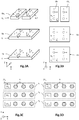
- the substrate 4 has an upper surface 4b formed by a monocrystalline material;
- the lower insulating layer 5 is made of a crystalline material epitaxied from the upper surface 4b of the substrate 4; and
- the nucleation conductive bands 6i are made of a material comprising a transition metal epitaxied from the crystalline material of the lower insulating layer 5.
- the substrate 4 comprises a monocrystalline growth material at least at the level of the upper surface 4b.
- the growth material is formed from a single crystal and therefore does not include several crystals separated from each other by grain boundaries.
- the material of the substrate 4 has crystallographic properties, in terms of lattice parameter and type of structure, suitable for the epitaxial growth of a crystalline material of the lower insulating layer 5.
- it preferably has a crystalline structure of the type. face-centered cubic oriented in the [111] direction or a hexagonal crystal structure oriented in the [0001] direction.
- the material of the substrate 4 is monocrystalline silicon, with a face-centered cubic-type crystal structure, the growth plane of which is oriented in the [111] direction, and the lattice parameter a s of which is approximately 3.84 ⁇ .
- the lower insulating layer 5 is made of a crystalline material epitaxied from the upper surface 4b of the substrate 4.
- the material of the lower insulating layer 5 comprises a crystal lattice in epitaxial relation with that of the monocrystalline material of the substrate.
- the crystal lattice of the material of the lower insulating layer 5 has an elementary cell defined in particular by its crystallographic axes denoted here, purely by way of illustration, a i , b i , c i .
- the crystal lattice therefore has an alignment of at least one crystallographic axis a i , b i oriented in the plane of the material and of at least one crystallographic axis c i oriented orthogonally to the plane of the material, with the crystallographic axes a s , b s and c s of the single crystal material of the substrate, respectively.
- This results in the fact that the crystallographic axis a i is substantially parallel, at any point of the upper surface 5b, to the crystallographic axis a s , just like, respectively, the crystallographic axes b i and c i relative to the axes crystallographic b s and c s .
- each crystallographic axis a i , b i , c i is substantially identical at all points of the upper surface 5b.
- the crystallographic axes a i are substantially identical, that is to say mutually parallel, at any point of the upper surface 5b, just like, respectively, the crystallographic axes b i and c i .
- a polycrystalline material is formed, unlike a monocrystalline material, of several crystals separated from each other by grain boundaries.
- the material of the lower insulating layer 5 exhibits crystallographic properties, in terms of lattice parameter and type of crystal structure, such that it is suitable for being epitaxied from the single crystal material of the substrate 4. It is furthermore suitable for allow the epitaxial growth of the nucleation conductive bands 6 i of a material comprising a transition metal from the upper surface 5b. It preferably has a lattice parameter such that the lattice mismatch with the monocrystalline material of the substrate 4 is less than or equal to 20%.
- the type of the crystal structure is such that its crystallographic axes a i , b i , c i can be respectively parallel to the axes a s , b s , c s of the single crystal material of the substrate.
- the crystal structure may be of the face-centered cubic type, oriented in the [111] direction, or of the hexagonal type oriented in the [0001] direction, or even of the orthorhombic type oriented in the [111] direction.
- the material of the lower insulating layer 5 is aluminum nitride AlN, with a mesh parameter of approximately 3.11 ⁇ , and with a crystalline structure of the hexagonal type, the growth plane of which is oriented in the [0001] direction.
- the nucleation conductive bands 6 i are made of a material comprising a transition metal epitaxied from the upper surface 5b of the lower insulating layer 5.
- the nucleation material comprises a crystal lattice epitaxially related to that of the material of the nucleation. lower insulating layer 5.
- the crystal lattice of the nucleating material has an elementary cell defined in particular by its crystallographic axes denoted here, purely by way of illustration, a n , b n , c n .
- the crystal lattice therefore has an alignment of at least one crystallographic axis a n , b n oriented in the plane of the material and at least one crystallographic axis c n oriented orthogonally to the plane of the material, with the crystallographic axes a i , b i , and c i , of the material of the lower insulating layer 5, respectively, at the level of the upper surface 5b.
- each crystallographic axis a n is identical at all points of the nucleation surface 6b.
- the crystallographic axes a n are identical, that is to say mutually parallel, at all points of the nucleation surface 6b, just like, respectively, the crystallographic axes b n and c n .
- the nucleation material exhibits crystallographic properties, in terms of lattice parameter and type of structure, such that it can be epitaxied from the material of the lower insulating layer 5. It is furthermore suitable for epitaxial growth, at from the nucleation surface 6b, of a wire 9. Preferably, it thus has a mesh parameter such that the mesh mismatch with the material of the lower insulating layer 5 is less than or equal to 20%.
- the type of the crystal structure is such that its crystallographic axes a n , b n , c n can be respectively parallel to the axes a i , b i , c i of the material of the lower insulating layer 5.
- the crystal structure can be respectively be of the face-centered cubic type, oriented in the direction [111] or of the hexagonal type oriented in the direction [0001], or even of the orthorhombic type oriented in the direction [111].
- the nucleation material comprises a transition metal, i.e. it can be a transition metal or a compound comprising a transition metal, for example a nitride or a carbide of a transition metal . Transition metals, as well as their nitrides and carbides, have in particular the advantage of good electrical conductivity, close to that of metals.
- the nucleation material can be chosen from titanium Ti, zirconium Zr, hafnium Hf, vanadium V, niobium Nb, tantalum Ta, chromium Cr, molybdenum Mo and tungsten W, a nitride of these elements TiN , ZrN, HfN, VN, NbN, TaN, CrN, MoN, or WN, or a carbide of these elements TiC, ZrC, HfC, VC, NbC, TaC, CrC, MoC, WC.
- the transition metal nitrides and carbides may contain an atomic proportion of transition metal other than 50%.
- the nucleation material is chosen from a nitride of titanium TiN, zirconium ZrN, hafnium HfN, vanadium VN, niobium NbN, tantalum TaN, chromium CrN, molybdenum MoN or tungsten WN, or a titanium TiN, zirconium ZrN, hafnium HfN, vanadium VN, niobium NbN, or tantalum TaN carbide.
- the nucleation material is chosen from a nitride or a carbide of titanium TiN, TiC, of zirconium ZrN, ZrC, of hafnium HfN, HfC, of vanadium VN, VC, of niobium NbN, NbC, or of tantalum TaN, TaC.
- the nucleation material is chosen from a nitride of titanium TiN, zirconium ZrN, hafnium HfN, niobium NbN, or tantalum TaN.
- the nucleation material is chosen from a hafnium HfN or niobium NbN nitride.
- the first doped portions 9 of the diodes 2 are epitaxied from the nucleation surfaces 6b of the various nucleation conductive bands 6 i .
- the wire material has a crystal lattice epitaxially related to that of the nucleation material.
- the crystal lattice of the wire material has an elementary mesh defined in particular by its crystallographic axes denoted here, purely by way of illustration, a f , b f , c f .
- the crystallographic axes a f , b f , c f of the wire material are respectively substantially parallel to the crystallographic axes a n , b n , c n of the nucleation material at the level of the nucleation surface 6b.
- the crystallographic axis a f is parallel to the crystallographic axis a n of the nucleation surface 6b. It is the same for the crystallographic axes b f and c f relative to the crystallographic axes b n and c n .
- each crystallographic axis a f , b f , c f is identical from one wire 9 to another.
- the crystallographic axes a f are identical, that is to say parallel to each other, from one wire to the other. It is the same for the crystallographic axes b n and c n .
- the wires exhibit substantially identical crystallographic properties, in terms of orientation and position of the crystal lattice.
- the optoelectronic device 1 thus exhibits substantially homogeneous crystallographic properties at the level of the wires, which helps to homogenize the electrical and / or optical properties of the light-emitting diodes 2.
- the transition metal nitride nucleation portions are epitaxial and not only textured when they are deposited on an epitaxial lower insulating layer, and not directly from it. the upper surface 4b of the single crystal material of the substrate.
- the epitaxial crystalline material comprises a crystal lattice, or crystal structure, in epitaxial relation with that of the nucleation material from which it is epitaxied.
- epitaxy relationship is meant that the epitaxial material exhibits an alignment of the crystallographic orientations of its crystal lattice, in at least one direction in the plane of the material and at least one direction orthogonal to the plane of the material, with those of the crystal lattice of the material. nucleation material.
- the plane of the epitaxial material is here a plane of growth of the material, parallel to the nucleation surface. The alignment is preferably carried out within 30 °, or even within 10 °.
- a crystalline material is epitaxied from a nucleating crystalline material, i.e.
- the epitaxial relationship between these two crystalline materials results in the fact that at least a crystallographic axis of the crystal lattice of the epitaxial material, oriented in the plane of the epitaxial material, for example a e and / or b e , and at least one crystallographic axis, oriented orthogonally to the plane, for example c e , are respectively substantially parallel to the crystallographic axes a n and / or b n , and c n of the crystal lattice of the nucleation material.
- An epitaxial material is a particular case of so-called textured materials in the sense that the textured materials have a preferential crystallographic direction oriented orthogonally to the plane of the material, but do not have a preferential crystallographic direction oriented in the plane of the material. Furthermore, the preferential crystallographic direction orthogonal to the plane of the textured material is not, or only slightly, dependent on the crystalline properties of the nucleation material. Thus, a textured material has a single preferred crystallographic direction, for example that of the c axis and not three preferred directions. The lattice of the textured material then has a polycrystalline structure in which the different crystalline domains, separated by grain boundaries, are all oriented along the same privileged crystallographic axis c.
- the c axes of the crystalline domains are mutually parallel but the a axes, like the b axes, are not mutually parallel and are oriented in a substantially random manner.
- This preferred crystallographic direction is not, or is not very dependent on the crystalline properties of the nucleation material.
- the wires 9, here in GaN epitaxied by MOCVD when they are epitaxied from a textured nucleation material and not epitaxied, all have the same direction of growth, the latter being substantially parallel to the crystallographic axis c n .
- the hexagonal shape of the wires 9 is not oriented identically from one wire to another, which reflects the fact that the crystallographic axes a f and b f are not respectively oriented in such a way. identical from one wire to another.
- the wires 9 then have crystallographic properties that are different from one wire to another, which can result in a certain inhomogeneity in the electrical and / or optical properties of the light-emitting diodes 2.
- the wires 9, here in GaN epitaxied by MOCVD when they are epitaxied from an epitaxial nucleation material and not textured, all have the same direction of growth, the latter being substantially parallel to the crystallographic axis c n .
- the hexagonal shape of the wires 9 is here oriented identically for all the wires 9, which reflects the fact that the crystallographic axes a f and b f are respectively oriented identically from one wire to the other. 'other.
- the wires 9 have crystallographic properties, in terms of orientation and position of the crystal lattice, which are substantially identical.
- the device optoelectronics 1 thus exhibits substantially homogeneous crystallographic properties at the level of the wires 9, which helps to homogenize the electrical and / or optical properties of the light-emitting diodes 2.
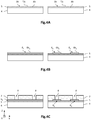
- FIGS. 4A to 4I schematically and partially illustrate, in cross section, various steps of an exemplary method of making the optoelectronic device 1 according to the preferred embodiment described above.
- Each figure illustrates a sectional view along the plane AA (left) and a sectional view along the plane BB (right).
- the substrate 4 is provided, the material of which is monocrystalline at least at the level of the upper surface.
- the substrate 4 is made of silicon, the structure of which is of the face-centered cubic type oriented in the direction [111]. Its mesh parameter in the plane of the upper surface is of the order of 3.84 ⁇ .
- the lower insulating layer 5 is deposited, so as to cover the upper surface of the substrate, by a method of the chemical vapor deposition (CVD) type, for example with organometallic precursors (MOCVD, for Metal-Organic Chemical Vapor Déposition, in English) or by a method of the epitaxy type by molecular beams (MBE, for Molecular-Beam Epitaxy, in English), of the hydride vapor phase epitaxy (HVPE, for Hybrid Vapor Phase Epitaxy) , in English), of the type epitaxy by atomic layer (ALE, for Atomic Layer Epitaxy, in English) or deposition by atomic layer (ALD, for Atomic Layer Deposition, in English), even by evaporation or by cathodic sputtering (sputtering, in English) English).
- CVD chemical vapor deposition
- MOCVD Metal-Organic Chemical Vapor Déposition
- MBE molecular beams
- HVPE hydride vapor phase
- the material of the lower insulating layer 5 is epitaxial aluminum nitride, the crystal structure of which is of the hexagonal type and is oriented in the [0001] direction. Its mesh parameter in the (X, Y) plane is of the order of 3.11 ⁇ . It is filed by MOCVD.
- the nominal V / III ratio defined as the ratio between the molar flux of elements from column V on the molar flux of elements from column III, i.e. here the N / Al ratio, is included between 200 and 1000.
- the pressure is of the order of 75 torr.
- the growth temperature T measured at the level of the substrate, may firstly be greater than or equal to 750 ° C. for the nucleation phase, then secondly of the order of 950 ° C. for the growth phase.
- the nucleation conductive bands 6i are formed on the upper surface of the lower insulating layer 5.
- the growth is carried out epitaxial of a layer of a nucleation material in a material comprising a transition metal, for example by a cathode sputtering technique, the growth temperature of which is advantageously between room temperature, for example 20 ° C, and 1000 ° C.
- the nucleation bands are also epitaxial when they are deposited by sputtering with a growth temperature between room temperature, for example 20 ° C, and 500 ° C, for example a temperature substantially equal to 400 ° vs.
- the power can be of the order of 400W.
- the pressure can be of the order of 8.10 -3 torr.
- High temperature sputtering and chemical vapor deposition techniques can also be used.
- the etching of the continuous layer of nucleation material is then carried out by conventional photolithography and etching techniques to form a plurality of nucleation conductive bands 6i distinct from each other.
- a crystallization annealing step can be carried out so as to obtain a monocrystalline nucleation material.
- the annealing can be carried out at an annealing temperature corresponding substantially to the crystallization temperature of the nucleation material, namely 1620 ° C. in the case here of the transition metal nitride.
- the crystallization of the nucleating material can also be obtained at an annealing temperature lower than the crystallization temperature, for example in a temperature range from 600 ° C to 1620 ° C, preferably between 800 ° C and 1200 ° C, for example equal to approximately 1000 ° C.
- the annealing can be carried out for a duration for example greater than 1 min, preferably greater than 5 min, or even 10 min, for example 20 min. It can be carried out under a flow of nitrogen (N2) and ammonia (NH3).
- the pressure can be of the order of 75 torr.
- the intermediate insulating layer 7 forming a growth mask is then deposited and the through openings 8 are produced.
- a layer of a dielectric material is thus deposited so as to cover the nucleation conductive bands 6i and the lower insulating layer 5, then through openings 8 are formed so as to open locally on the nucleation surfaces.
- the dielectric material is, for example, a silicon oxide (for example SiO2) or a silicon nitride (for example Si3N4), or even a stack of several different dielectric materials. It is selectively etched with respect to the material of the nucleation conductive bands 6i.
- the lateral dimensions of the openings are smaller than the width of the conductive nucleation bands 6i, for example at least two times smaller.
- the wires 9 are formed, here in GaN, by epitaxial growth from the nucleation surfaces of the various nucleation conductive bands 6 i , through the openings of the intermediate insulating layer 7, for example according to a process identical or similar to that described in the document WO2012 / 136665 .
- the growth temperature is brought to a first value T 1 , for example between 950 ° C and 1100 ° C, and in particular between 990 ° C and 1060 ° C.
- the nominal V / III ratio here the N / Ga ratio, has a first value (V / III) 1 of between 10 and 100 approximately, for example approximately equal to 30.
- the elements of group III and of group V come from precursors injected into the epitaxy reactor, for example trimethylgallium (TMGa) or triethylgallium (TEGa) for gallium, and ammonia (NH 3 ) for nitrogen.
- TMGa trimethylgallium
- TMGa triethylgallium
- NH 3 ammonia
- the H 2 / N 2 ratio has a first value (H 2 / N 2 ) 1 greater than or equal to 60/40, preferably greater than or equal to 70/30, or even more, for example substantially equal to 90/10.
- the pressure can be set at around 100mbar.
- first doped portions 9 are obtained in the form of wires which extend along the longitudinal axis ⁇ from the nucleation surfaces.
- the first semiconductor compound of the first doped portions 9, namely here GaN, is n-type doped with silicon.
- the lower part 12 of the wires 9 is located in the openings of the intermediate insulating layer 7, and extends along the longitudinal axis ⁇ by the upper part 13.
- the upper part 13 of the wires 9 is located in the openings of the intermediate insulating layer 7, and extends along the longitudinal axis ⁇ by the upper part 13.
- the active zones are formed by epitaxial growth from the exposed surface of the wires 9, that is to say here on the upper part 13 of the wires 9. More precisely, a stack of barrier layers and at least a layer forming a quantum well, said layers being alternated in the direction of epitaxial growth.
- the layers forming the quantum wells and the barrier layers can be made of InGaN, with different atomic proportions for the quantum well layers and the barrier layers.
- the barrier layers are made of In x Ga (1-x) N with x equal to approximately 18 atomic%
- the quantum well layers are also made of In y Ga (1-y) N, with y greater than x, for example of the order of 25 atomic%, so as to improve the quantum confinement of the charge carriers in the quantum wells.
- the formation of the barrier layers and of the quantum well layers can be carried out at a growth temperature value T 3 substantially equal to the value T 2 , namely here 750 ° C.
- the V / III ratio has a value (V / III) 3 substantially equal to the value (V / III) 2 .
- the H 2 / N 2 ratio has a value substantially equal to the value (H 2 / N 2 ) 2 during the formation of the barrier layers and has a value substantially less than the value (H 2 / N 2 ) 2 during the formation of quantum well layers, for example 1/99.
- the pressure can remain unchanged. In this way, barrier layers of InGaN with approximately 18 atomic% indium are obtained and quantum well layers of InGaN with approximately 25 atomic% indium.
- the second p-doped portions are then formed by epitaxial growth so as to cover and at least partially surround the active areas.
- the growth temperature can be brought to a fourth value T 4 greater than the value T 3 , for example of the order of 885 ° C.
- the V / III ratio can be brought to a fourth value (V / III) 4 greater than the value (V / III) 3 , for example of the order of 4000.
- the H 2 / N 2 ratio is increased to a fourth value (H 2 / N 2 ) 4 greater than the value (H 2 / N 2 ) 2 , for example of the order of 15/85.
- the pressure can be reduced to a value of the order of 300mbar.
- p-doped second portions 11 are obtained, for example made of GaN or p-type doped InGaN, which here continuously cover and surround the active areas.
- the second p-doped portions 11 and the active areas thus form the shells of the diodes 2 in the core / shell configuration.
- the active zone and the second doped portion 11 of the diodes 2 cover the upper part 13 of each wire, from the upper surface of the intermediate insulating layer 7.
- the upper conductive strips 14 j distinct from each other, which extend over the upper surface of the intermediate insulating layer 7 and come into contact with the second doped portions 11 of diodes.
- a continuous layer of a conductive material and here partially transparent to the light radiation emitted by the diodes is deposited in a conformal manner.
- the upper conductive strips 14 j which are distinct from each other, are formed. They comprise here each of the parts which cover the second doped portions 11 of a set D j of diodes, these covering parts 15 j being connected in pairs by connecting parts 16 j which extend over the upper surface of the layer. intermediate insulation 7.
- the connecting parts 16 j of the upper conductive strips 14 j are covered by a metal layer 17 adapted to reduce the electrical resistance of the upper conductive strips 14 j and thus improve the flow of electric current.
- This metal layer 17 is deposited on the upper conductive strips 14 j and then is etched so as to cover only the connecting parts 16 j and not the covering parts 15 j .
- This metal layer 17 can be made of one or more materials chosen from aluminum, silver, gold or any other suitable material, and has a thickness for example between 5nm and 200nm, preferably between 10nm and 100nm, for example equal to approximately 30nm.
- the layer metal 17 can be deposited prior to the deposition of the upper conductive strips 14 j . It is etched so as not to extend around the second doped portions 11 along the Z axis.
- the upper insulating layer 18 is deposited so as to continuously cover the upper conductive strips 14 j , the metal layer 17 and the intermediate insulating layer 7.
- the upper insulating layer 18 is made of a dielectric material such as, for example, , a silicon oxide (for example SiO2) or a silicon nitride (for example Si3N4), or even a stack of several different dielectric materials.
- a reflective layer 19 is then deposited so as to cover the surface of the upper insulating layer 18 without covering the wires 9.
- the reflective layer 19 thus extends essentially in the plane (X, Y).
- This reflective layer 19 can be made of one or more materials chosen from aluminum, silver, gold or any other suitable material, and has a thickness for example between 20nm and 1500nm, preferably between 400nm and 800nm. The thickness of the reflective layer 19 is chosen so that the incident light radiation emitted by the diodes 2 is reflected in the + Z direction.
- an encapsulation layer 20 is deposited so as to completely cover the diodes.
- the encapsulation layer 20 is made of a dielectric material transparent to the light radiation emitted by the diodes 2, such as, for example, a silicon oxide (for example SiO2) or a silicon nitride (for example Si3N4), or even a stacking of several different dielectric materials.
- the thickness of the encapsulation layer 20 is for example between 250 nm and 50 ⁇ m.
- the first connection pads 21 i and the second connection pads 25 j are then carried out .
- the substrate 4 is thinnered, then the first through orifices 22 i are produced, opening out at the level of the conductive nucleation bands 6 i as well as the second through orifices 26 j emerging at the level of the upper conductive strips 14 j .
- the sides of the through-holes can be coated with an insulating layer 24, then a conductive material 23 fills the interior of the through-holes.
- the first and second connection pads 21 i and 25 j are then formed, respectively, at each first and second orifice passing through 22 i and 26 j .
- Hybridization of the support to an integrated control circuit is then carried out by molecular bonding, by wiring by wire, or by connection by means of conductive elements and fuses.
- the method for producing the optoelectronic device 1 has the advantage of not having to carry out an electrical individualization of the diodes 2 by means of insulating trenches formed between the diodes 2 from the front face 3b of the support.
- the diodes 2 are here individualized by the first and second electrodes which are in the form of conductive strips distinct from each other.
- the support has improved mechanical strength, which in particular facilitates hybridization to the control circuit.
- the diodes 2 have optical and / or electronic properties preserved insofar as the individualization of the diodes 2 does not require, as in the example of the prior art mentioned above, an etching of the doped portions and of the active area.
- the homogeneity of the optical and / or electronic properties of the diodes 2 is further improved when the diodes 2 are formed from conductive bands of nucleation 6i in epitaxial relation with the monocrystalline material of the substrate.
- each pixel P ij can include several diodes.
- the application of a potential difference to the pixel P ij leads to an activation of the diodes 2 of this pixel, the diodes 2 of the other pixels remaining deactivated.
- the optoelectronic device 1 may include an integrated routing circuit 28 comprising electrical interconnections 29 ensuring a series connection of several pixels between them.
- the diodes 2 of the pixel P 1 are connected in series with the diodes 2 of the pixel P 2 by means of the electrical interconnections 29 of the routing circuit 28 connected to the first and second through orifices 22 i , 26 j .
- the integrated routing circuit 28 can be assembled and electrically connected to the control circuit (not shown) by means of the connection pads 21 i , 25 j .
- a potential difference can be applied to the pixels P1 and P2 connected in series, by means of the connection pads 21 2 and 25 1 .
- connection pad 25 1 is applied to the upper conductive strip 14 1 of the pixel P 1 via the through-hole 26 1 and the interconnection 29.1
- the electrical potential of the connection pad 21 2 is applied to the nucleation conductive strip 6 2 of the pixel P 2 via the through orifice 22 2 and the interconnection 29.3.
- the pixels P 1 and P 2 are connected in series by the electrical connection of the nucleation conductive strip 6 1 of the pixel P 1 with the upper conductive strip 14 2 of the pixel P 2 made by the through holes 22 1 and 26 2 and l 'interconnection 29.2.
- the interconnection 29.2 can be omitted and the through holes 22 1 and 26 2 can be in electrical contact directly in the substrate 4.
- the optoelectronic device 1 can comprise one or more electrical interconnections 30 located at the level of the intermediate insulating layer 7, allowing, in this example, the placing in series of the diodes 2 of the pixel P 1 with the diodes 2 of the pixel P 2 .
- the electrical interconnection 30 is formed here of a through orifice filled with a conductive material opening on the one hand on the nucleation conductive strip 6 1 of the pixel P 1 and on the other hand on the upper conductive strip 14 2 of the pixel P 2 .
- a routing circuit 28 is provided and ensures the electrical polarization of the pixels P 1 and P 2 connected in series, by means of the interconnections 29.1 and 29.3.
- Examples of figures 6A and 6B are given purely by way of illustration and other electrical interconnection configurations internal or formed in an integrated routing circuit are possible so as to ensure a connection of the pixels in series or in parallel. Furthermore, as a variant and as mentioned above, the electrical connection pads can be located on the front face or on the rear face of the support.
- an optoelectronic device 1 with light-emitting diodes 2 which can advantageously form a display screen or an image projector with high light intensity and high spatial resolution.
- the invention also applies to the field of photodiodes adapted to receive and detect light radiation and to convert it into electrical signals relating to the various pixels.
- Three-dimensional diodes 2 of the wire type have been described, but the invention also applies to the first doped portions in the form of three-dimensional pads whose height along the Z axis is of the same order of magnitude as its transverse dimensions in the plane ( X, Y), as well as to the first doped portions in the form of possibly truncated pyramids.
- Diodes 2 in core / shell configuration have been described where the active areas and the second doped portions cover the sides and the top of the wires 9.
- the invention also applies to the axial configuration of the diodes 2 where the active areas and the second doped portions cover only the top of the wires.
- nucleation conductive bands vis-à-vis the upper conductive bands
- other orientations are possible, where the nucleation bands and the upper bands form for example two by two an angle non-zero less than or greater than 90 °.
Landscapes
- Led Devices (AREA)
Claims (15)
- Optoelektronische Vorrichtung (1), die aufweist:- einen Träger, der gegenüberliegende so genannte Rück- (3a) und Vorderseiten (3b) aufweist;- eine Vielzahl erster Leitungsbänder (6i), die erste Polarisationselektroden bilden, die sich voneinander unterscheiden und auf der Vorderseite (3b) ruhen, hergestellt aus einem elektrisch leitenden Material;- eine isolierende Zwischenschicht (7), die die ersten Leitungsbänder (6i) bedeckt und Durchgangsöffnungen (8) aufweist, die auf die ersten Leitungsbänder (6i) münden;- eine Vielzahl von Dioden (2), die je einen ersten dreidimensionalen dotierten Abschnitt (9) und einen zweiten dotierten Abschnitt (11) aufweisen, die so angeordnet sind, dass sie einen p-n-Übergang formen, wobei die ersten dotierten Abschnitte (9) durch die Durchgangsöffnungen (8) hindurch mit den ersten Leitungsbändern (6i) in Kontakt sind und sich gemäß einer Längsachse im Wesentlichen orthogonal zur Vorderseite (3b) erstrecken;- eine Vielzahl oberer Leitungsbänder (14j), die zweite Polarisationselektroden bilden, die sich voneinander unterscheiden und auf der isolierenden Zwischenschicht (7) ruhen, wobei jedes obere Leitungsband (14j) so angeordnet ist, dass es mit zweiten dotierten Abschnitten (11) einer Einheit von Dioden (2) in Kontakt ist, deren erste dotierte Abschnitte (9) mit verschiedenen ersten Leitungsbändern (6i) in Kontakt sind; dadurch gekennzeichnet, dass die ersten Leitungsbänder (6i) Nukleations-Leitungsbänder sind, die aus einem elektrisch leitenden Material hergestellt sind, das für das Wachsen der ersten dotierten Abschnitte (9) der Dioden (2) geeignet ist.
- Optoelektronische Vorrichtung (1) nach Anspruch 1, wobei der Träger ein elektrisch isolierendes Substrat (4) aufweist, von dem eine Oberseite (4b) die Vorderseite (3b) bildet, oder eine Schicht oder ein Substrat (4), halbleitend oder elektrisch leitend, aufweist, das mit einer so genannten unteren isolierenden Schicht (5) beschichtet ist, von der eine Seite die Vorderseite (3b) bildet.
- Optoelektronische Vorrichtung (1) nach Anspruch 1 oder 2, wobei jedes Nukleations-Leitungsband (6i) sich in Längsrichtung auf der Vorderseite (3b) erstreckt und durch die isolierende Zwischenschicht (7) von seinen Nachbarn in Querrichtung elektrisch getrennt wird.
- Optoelektronische Vorrichtung (1) nach einem der Ansprüche 1 bis 3, wobei jedes obere Leitungsband (14j) sich in Längsrichtung auf der isolierenden Zwischenschicht (7) erstreckt und durch eine so genannte obere isolierende Schicht (18) von seinen Nachbarn in Querrichtung elektrisch getrennt wird.
- Optoelektronische Vorrichtung (1) nach einem der Ansprüche 1 bis 4, wobei die oberen Leitungsbänder (14j) aus einem zumindest teilweise transparenten leitenden Material sind und die zweiten dotierten Abschnitte (11) zumindest teilweise abdecken.
- Optoelektronische Vorrichtung (1) nach Anspruch 5, wobei jedes obere Leitungsband (14j) Teile (15j) aufweist, die die zweiten dotierten Abschnitte (11) einer Einheit von Dioden (2) abdecken, wobei die abdeckenden Teile (15j) durch so genannte Verbindungsteile (16j) miteinander verbunden sind, die auf der isolierenden Zwischenschicht (7) ruhen.
- Optoelektronische Vorrichtung (1) nach Anspruch 6, wobei die Verbindungsteile (16j) der oberen Leitungsbänder (14j) zumindest zum Teil mit einer Metallschicht (19) beschichtet sind.
- Optoelektronische Vorrichtung (1) nach einem der Ansprüche 1 bis 7, die erste Anschlusskontakte (21i) aufweist, die auf der Rückseite (3a) ruhen und mit den Nukleations-Leitungsbändern (6i) durch erste Öffnungen (22i) elektrisch verbunden sind, die den Träger durchqueren und mit einem leitenden Material gefüllt sind, und/oder zweite Anschlusskontakte (25j) aufweist, die auf der Rückseite (3a) ruhen und mit den oberen Leitungsbänder (14j) durch zweite Öffnungen (26j) elektrisch verbunden sind, die den Träger und die isolierende Zwischenschicht (7) durchqueren und mit einem leitenden Material gefüllt sind.
- Optoelektronische Vorrichtung (1) nach einem der Ansprüche 1 bis 8, die einen integrierten Steuerschaltkreis aufweist, der mit dem Träger zusammengebaut und mit den Nukleations-Leitungsbändern (6i) und den oberen Leitungsbändern (14j) elektrisch verbunden ist, geeignet, um sequentiell eine Potentialdifferenz an verschiedene Teileinheiten (Pij) von Dioden (2) anzuwenden, wobei die Diode oder die Dioden (2) einer gleichen Teileinheit (Pij) mit einem gleichen Nukleations-Leitungsband (6i) und einem gleichen oberen Leitungsband (14j) in Kontakt ist(sind), wobei die Diode oder die Dioden (2) verschiedener Teileinheiten mit verschiedenen Nukleations-Leitungsbändern (6i) und/oder verschiedenen oberen Leitungsbändern (14j) in Kontakt sind.
- Optoelektronische Vorrichtung (1) nach einem der Ansprüche 1 bis 9, wobei mindestens eine Diode (2ij) in Kontakt mit einem ersten Nukleations-Leitungsband (6i) und einem ersten oberen Leitungsband (14j) mit mindestens einer weiteren Diode (2i'j') in Reihe geschaltet ist, wobei diese mit einem zweiten Nukleations-Leitungsband (6i'≠i) anders als das erste Nukleationsband (6i) und einem zweiten oberen Leitungsband (14j'≠j) anders als das erste obere Band (14j) in Kontakt ist.
- Optoelektronische Vorrichtung (1) nach einem der Ansprüche 1 bis 10, wobei der Träger von einem Substrat (4) aus einem monokristallinen Material gebildet wird, das eine Oberfläche (4b) bildet, auf der eine so genannte untere isolierende Schicht (5) aus einem dielektrischen Material ruht, epitaxiert ausgehend von der Oberfläche (4b) des Substrats und eine gegenüberliegende Oberfläche (5b) bildend, wobei die Nukleations-Leitungsbänder (6i) aus einem Material sind, das ein Übergangsmetall aufweist, das ein kristallines Nukleationsmaterial bildet, epitaxiert ausgehend von der Oberfläche (5b) der unteren isolierenden Schicht (5) und eine Nukleationsfläche (6bi) bildend, auf der die ersten dotierten Abschnitte (9) der Dioden (2) in Kontakt sind.
- Optoelektronische Vorrichtung (1) nach Anspruch 11, wobei das Material der unteren isolierenden Schicht (5) ausgewählt wird aus Aluminiumnitrid und den Aluminium-, Titan-, Hafnium-, Magnesium- und Zirkonoxiden, und eine hexagonale, kubisch-flächenzentrierte oder orthorhombische Kristallstruktur aufweist.
- Optoelektronische Vorrichtung (1) nach Anspruch 11 oder 12, wobei das Material der Nukleations-Leitungsbänder (6i) ausgewählt wird aus Titan, Vanadium, Chrom, Zirkon, Niob, Molybdän, Hafnium, Tantal und Wolfram, oder aus einem Nitrid oder Karbid von Titan, Vanadium, Chrom, Zirkon, Niob, Molybdän, Hafnium, Tantal und Wolfram, und eine hexagonale oder kubisch-flächenzentrierte Kristallstruktur aufweist, oder ein Material auf der Basis von Galliumnitrid ist.
- Optoelektronische Vorrichtung (1) nach einem der Ansprüche 11 bis 13, wobei das monokristalline Material des Substrats (4) ausgewählt wird aus einer III-V-Verbindung, einer II-VI-Verbindung, oder einem IV-Element oder einer IV-Verbindung, und eine hexagonale oder kubisch-flächenzentrierte Kristallstruktur aufweist.
- Verfahren zur Herstellung der optoelektronischen Vorrichtung (1) nach einem der Ansprüche 1 bis 14, das einen Schritt des epitaxialen Wachstums der Nukleations-Leitungsbänder (6) durch Kathodenzerstäubung bei einer Wachstumstemperatur zwischen der Umgebungstemperatur und 500°C aufweist.
Applications Claiming Priority (2)
| Application Number | Priority Date | Filing Date | Title |
|---|---|---|---|
| FR1656218A FR3053531B1 (fr) | 2016-06-30 | 2016-06-30 | Dispositif optoelectronique a diodes tridimensionnelles |
| PCT/FR2017/051693 WO2018002498A1 (fr) | 2016-06-30 | 2017-06-26 | Dispositif optoelectronique a diodes tridimensionnelles |
Publications (2)
| Publication Number | Publication Date |
|---|---|
| EP3479409A1 EP3479409A1 (de) | 2019-05-08 |
| EP3479409B1 true EP3479409B1 (de) | 2021-08-04 |
Family
ID=57583152
Family Applications (1)
| Application Number | Title | Priority Date | Filing Date |
|---|---|---|---|
| EP17742491.8A Active EP3479409B1 (de) | 2016-06-30 | 2017-06-26 | Optoelektronische vorrichtung mit dreidimensionalen dioden |
Country Status (6)
| Country | Link |
|---|---|
| US (1) | US10886427B2 (de) |
| EP (1) | EP3479409B1 (de) |
| KR (1) | KR102429890B1 (de) |
| CN (1) | CN109417084B (de) |
| FR (1) | FR3053531B1 (de) |
| WO (1) | WO2018002498A1 (de) |
Families Citing this family (14)
| Publication number | Priority date | Publication date | Assignee | Title |
|---|---|---|---|---|
| KR102699567B1 (ko) * | 2016-07-11 | 2024-08-29 | 삼성디스플레이 주식회사 | 초소형 발광 소자를 포함하는 픽셀 구조체, 표시장치 및 그 제조방법 |
| KR102587958B1 (ko) * | 2017-02-03 | 2023-10-11 | 삼성전자주식회사 | 메타 광학 소자 및 그 제조 방법 |
| CN110832660B (zh) * | 2017-05-17 | 2023-07-28 | Oti照明公司 | 在图案化涂层上选择性沉积传导性涂层的方法和包括传导性涂层的装置 |
| FR3076078B1 (fr) * | 2017-12-27 | 2021-11-26 | Aledia | Dispositif optoelectronique a matrice de diodes tridimensionnelles |
| CN109979957B (zh) * | 2019-03-15 | 2024-05-17 | 广东省半导体产业技术研究院 | 半导体发光器件及其制作方法 |
| FR3098013B1 (fr) * | 2019-06-25 | 2021-07-02 | Commissariat Energie Atomique | Procédé de fabrication d'un dispositif optoélectronique à diodes électroluminescentes de type axial |
| WO2021084049A1 (en) | 2019-10-29 | 2021-05-06 | Osram Opto Semiconductors Gmbh | An optoelectronic device |
| WO2021110333A1 (en) | 2019-12-06 | 2021-06-10 | Osram Opto Semiconductors Gmbh | Optoelectronic device |
| DE112020005978T5 (de) | 2019-12-06 | 2022-09-22 | Osram Opto Semiconductors GmbH | Fenster oder oberfläche eines fahrzeugs mit mindestens einem optoelektronischen bauelement |
| WO2021110334A1 (en) | 2019-12-06 | 2021-06-10 | Osram Opto Semiconductors Gmbh | Apparatus comprising a carrier with optoelectronic elements and method for manufacturing the apparatus |
| US12388058B2 (en) * | 2019-12-06 | 2025-08-12 | Osram Opto Semiconductors Gmbh | Optoelectronic device |
| FR3125921B1 (fr) | 2021-07-30 | 2023-07-07 | Commissariat Energie Atomique | Procédé de fabrication d’un dispositif optoélectronique comportant une étape de réalisation d’une couche mince conductrice de manière conforme et continue par dépôt directif |
| KR102567895B1 (ko) * | 2021-08-19 | 2023-08-17 | 청주대학교 산학협력단 | 분산 마이크로 전극 그리드를 갖는 3차원 투명 태양전지 |
| KR20230033773A (ko) * | 2021-09-01 | 2023-03-09 | 삼성디스플레이 주식회사 | 발광 소자 및 이를 포함하는 표시 장치 |
Family Cites Families (16)
| Publication number | Priority date | Publication date | Assignee | Title |
|---|---|---|---|---|
| US20110127544A1 (en) * | 2008-05-06 | 2011-06-02 | Kyma Technologies | Group iii nitride templates and related heterostructures, devices, and methods for making them |
| DE102011007271B4 (de) * | 2010-04-19 | 2022-08-11 | Electronics And Telecommunications Research Institute | Feldeffekttransistor mit variablem Gate |
| FR2973936B1 (fr) | 2011-04-05 | 2014-01-31 | Commissariat Energie Atomique | Procede de croissance selective sur une structure semiconductrice |
| KR101258583B1 (ko) * | 2011-10-21 | 2013-05-02 | 삼성전자주식회사 | 나노 로드 발광 소자 및 그 제조 방법 |
| KR101269053B1 (ko) * | 2011-11-09 | 2013-06-04 | 삼성전자주식회사 | 나노 로드 발광 소자 및 그 제조 방법 |
| FR2984599B1 (fr) * | 2011-12-20 | 2014-01-17 | Commissariat Energie Atomique | Procede de fabrication d'un micro- ou nano- fil semiconducteur, structure semiconductrice comportant un tel micro- ou nano- fil et procede de fabrication d'une structure semiconductrice |
| DE102012109594A1 (de) * | 2012-10-09 | 2014-04-10 | Osram Opto Semiconductors Gmbh | Verfahren zur Herstellung eines optoelektronischen Halbleiterbauteils und optoelektronisches Halbleiterbauteil |
| US9537044B2 (en) * | 2012-10-26 | 2017-01-03 | Aledia | Optoelectric device and method for manufacturing the same |
| FR3005788B1 (fr) * | 2013-05-14 | 2016-10-21 | Commissariat Energie Atomique | Dispositif optoelectronique et son procede de fabrication |
| FR3011381B1 (fr) * | 2013-09-30 | 2017-12-08 | Aledia | Dispositif optoelectronique a diodes electroluminescentes |
| US9099573B2 (en) | 2013-10-31 | 2015-08-04 | Samsung Electronics Co., Ltd. | Nano-structure semiconductor light emitting device |
| US9450147B2 (en) * | 2013-12-27 | 2016-09-20 | Apple Inc. | LED with internally confined current injection area |
| EP2960950B1 (de) | 2014-06-26 | 2023-01-25 | AZUR SPACE Solar Power GmbH | Mehrfach-solarzelle |
| CN104900746B (zh) * | 2015-05-14 | 2017-04-12 | 南京大学 | 一种基于径向结叠层结构的三原色光电探测方法 |
| WO2017031265A1 (en) * | 2015-08-18 | 2017-02-23 | Wake Forest University | Frequency dependent light emitting devices |
| US20170207365A1 (en) * | 2016-01-20 | 2017-07-20 | Google Inc. | Layered active region light emitting diode |
-
2016
- 2016-06-30 FR FR1656218A patent/FR3053531B1/fr not_active Expired - Fee Related
-
2017
- 2017-06-26 CN CN201780040945.8A patent/CN109417084B/zh active Active
- 2017-06-26 US US16/313,749 patent/US10886427B2/en active Active
- 2017-06-26 WO PCT/FR2017/051693 patent/WO2018002498A1/fr not_active Ceased
- 2017-06-26 KR KR1020197002890A patent/KR102429890B1/ko active Active
- 2017-06-26 EP EP17742491.8A patent/EP3479409B1/de active Active
Also Published As
| Publication number | Publication date |
|---|---|
| KR102429890B1 (ko) | 2022-08-04 |
| FR3053531A1 (fr) | 2018-01-05 |
| US20190172970A1 (en) | 2019-06-06 |
| CN109417084B (zh) | 2023-09-19 |
| EP3479409A1 (de) | 2019-05-08 |
| WO2018002498A1 (fr) | 2018-01-04 |
| US10886427B2 (en) | 2021-01-05 |
| CN109417084A (zh) | 2019-03-01 |
| KR20190089839A (ko) | 2019-07-31 |
| FR3053531B1 (fr) | 2018-08-17 |
Similar Documents
| Publication | Publication Date | Title |
|---|---|---|
| EP3646383B1 (de) | Optoelektronische vorrichtung mit dreidimensionalen halbleiterstrukturen in axialer anordnung | |
| EP3782193B1 (de) | Herstellungsverfahren einer optoelektronischen vorrichtung mit diodenmatrix | |
| EP3479409A1 (de) | Optoelektronische vorrichtung mit dreidimensionalen dioden | |
| EP3053200B1 (de) | Optoelektronisches bauteil mit leuchtdioden | |
| EP3384537B1 (de) | Optoelektronische vorrichtung mit tridimensionalen halbleiterstrukturen in axialer konfiguration | |
| EP3248227B1 (de) | Optoelektronisches halbleiterbauelement und herstellungsverfahren davon | |
| FR3061607A1 (fr) | Dispositif optoelectronique a diodes electroluminescentes | |
| WO2018002497A1 (fr) | Structure de nucleation adaptee a la croissance epitaxiale d'elements semiconducteurs tridimensionnels | |
| EP3891813A1 (de) | Mehrfarbige elektrolumineszierende anzeigevorrichtung und verfahren zur herstellung einer solchen vorrichtung | |
| EP3347917B1 (de) | Elektrolumineszente vorrichtung mit integriertem lichtsensor | |
| EP3732725B1 (de) | Optoelektronische vorrichtung mit einer matrix aus dreidimensionalen dioden | |
| EP3053201B1 (de) | Optoelektronische vorrichtung mit leuchtdioden | |
| WO2017093645A1 (fr) | Dispositif optoelectronique comportant des structures semiconductrices tridimensionnelles a portion monocristalline elargie | |
| WO2019002720A1 (fr) | Dispositif optoelectronique | |
| FR3114682A1 (fr) | Dispositif optoelectronique a diodes electroluminescentes a affichage couleur | |
| EP4082047B1 (de) | Dreidimensionale optoelektronische bauelementevorrichtung zum laserschneiden und verfahren zum laserschneiden einer solchen vorrichtung |
Legal Events
| Date | Code | Title | Description |
|---|---|---|---|
| STAA | Information on the status of an ep patent application or granted ep patent |
Free format text: STATUS: UNKNOWN |
|
| STAA | Information on the status of an ep patent application or granted ep patent |
Free format text: STATUS: THE INTERNATIONAL PUBLICATION HAS BEEN MADE |
|
| PUAI | Public reference made under article 153(3) epc to a published international application that has entered the european phase |
Free format text: ORIGINAL CODE: 0009012 |
|
| STAA | Information on the status of an ep patent application or granted ep patent |
Free format text: STATUS: REQUEST FOR EXAMINATION WAS MADE |
|
| 17P | Request for examination filed |
Effective date: 20181221 |
|
| AK | Designated contracting states |
Kind code of ref document: A1 Designated state(s): AL AT BE BG CH CY CZ DE DK EE ES FI FR GB GR HR HU IE IS IT LI LT LU LV MC MK MT NL NO PL PT RO RS SE SI SK SM TR |
|
| AX | Request for extension of the european patent |
Extension state: BA ME |
|
| DAV | Request for validation of the european patent (deleted) | ||
| DAX | Request for extension of the european patent (deleted) | ||
| GRAP | Despatch of communication of intention to grant a patent |
Free format text: ORIGINAL CODE: EPIDOSNIGR1 |
|
| STAA | Information on the status of an ep patent application or granted ep patent |
Free format text: STATUS: GRANT OF PATENT IS INTENDED |
|
| INTG | Intention to grant announced |
Effective date: 20210305 |
|
| GRAS | Grant fee paid |
Free format text: ORIGINAL CODE: EPIDOSNIGR3 |
|
| GRAA | (expected) grant |
Free format text: ORIGINAL CODE: 0009210 |
|
| STAA | Information on the status of an ep patent application or granted ep patent |
Free format text: STATUS: THE PATENT HAS BEEN GRANTED |
|
| AK | Designated contracting states |
Kind code of ref document: B1 Designated state(s): AL AT BE BG CH CY CZ DE DK EE ES FI FR GB GR HR HU IE IS IT LI LT LU LV MC MK MT NL NO PL PT RO RS SE SI SK SM TR |
|
| REG | Reference to a national code |
Ref country code: GB Ref legal event code: FG4D Free format text: NOT ENGLISH |
|
| REG | Reference to a national code |
Ref country code: AT Ref legal event code: REF Ref document number: 1417877 Country of ref document: AT Kind code of ref document: T Effective date: 20210815 |
|
| REG | Reference to a national code |
Ref country code: CH Ref legal event code: EP |
|
| REG | Reference to a national code |
Ref country code: DE Ref legal event code: R096 Ref document number: 602017043381 Country of ref document: DE |
|
| REG | Reference to a national code |
Ref country code: IE Ref legal event code: FG4D Free format text: LANGUAGE OF EP DOCUMENT: FRENCH |
|
| REG | Reference to a national code |
Ref country code: LT Ref legal event code: MG9D |
|
| REG | Reference to a national code |
Ref country code: NL Ref legal event code: MP Effective date: 20210804 |
|
| REG | Reference to a national code |
Ref country code: AT Ref legal event code: MK05 Ref document number: 1417877 Country of ref document: AT Kind code of ref document: T Effective date: 20210804 |
|
| PG25 | Lapsed in a contracting state [announced via postgrant information from national office to epo] |
Ref country code: HR Free format text: LAPSE BECAUSE OF FAILURE TO SUBMIT A TRANSLATION OF THE DESCRIPTION OR TO PAY THE FEE WITHIN THE PRESCRIBED TIME-LIMIT Effective date: 20210804 Ref country code: SE Free format text: LAPSE BECAUSE OF FAILURE TO SUBMIT A TRANSLATION OF THE DESCRIPTION OR TO PAY THE FEE WITHIN THE PRESCRIBED TIME-LIMIT Effective date: 20210804 Ref country code: RS Free format text: LAPSE BECAUSE OF FAILURE TO SUBMIT A TRANSLATION OF THE DESCRIPTION OR TO PAY THE FEE WITHIN THE PRESCRIBED TIME-LIMIT Effective date: 20210804 Ref country code: AT Free format text: LAPSE BECAUSE OF FAILURE TO SUBMIT A TRANSLATION OF THE DESCRIPTION OR TO PAY THE FEE WITHIN THE PRESCRIBED TIME-LIMIT Effective date: 20210804 Ref country code: BG Free format text: LAPSE BECAUSE OF FAILURE TO SUBMIT A TRANSLATION OF THE DESCRIPTION OR TO PAY THE FEE WITHIN THE PRESCRIBED TIME-LIMIT Effective date: 20211104 Ref country code: LT Free format text: LAPSE BECAUSE OF FAILURE TO SUBMIT A TRANSLATION OF THE DESCRIPTION OR TO PAY THE FEE WITHIN THE PRESCRIBED TIME-LIMIT Effective date: 20210804 Ref country code: NO Free format text: LAPSE BECAUSE OF FAILURE TO SUBMIT A TRANSLATION OF THE DESCRIPTION OR TO PAY THE FEE WITHIN THE PRESCRIBED TIME-LIMIT Effective date: 20211104 Ref country code: PT Free format text: LAPSE BECAUSE OF FAILURE TO SUBMIT A TRANSLATION OF THE DESCRIPTION OR TO PAY THE FEE WITHIN THE PRESCRIBED TIME-LIMIT Effective date: 20211206 Ref country code: FI Free format text: LAPSE BECAUSE OF FAILURE TO SUBMIT A TRANSLATION OF THE DESCRIPTION OR TO PAY THE FEE WITHIN THE PRESCRIBED TIME-LIMIT Effective date: 20210804 Ref country code: ES Free format text: LAPSE BECAUSE OF FAILURE TO SUBMIT A TRANSLATION OF THE DESCRIPTION OR TO PAY THE FEE WITHIN THE PRESCRIBED TIME-LIMIT Effective date: 20210804 |
|
| PG25 | Lapsed in a contracting state [announced via postgrant information from national office to epo] |
Ref country code: PL Free format text: LAPSE BECAUSE OF FAILURE TO SUBMIT A TRANSLATION OF THE DESCRIPTION OR TO PAY THE FEE WITHIN THE PRESCRIBED TIME-LIMIT Effective date: 20210804 Ref country code: LV Free format text: LAPSE BECAUSE OF FAILURE TO SUBMIT A TRANSLATION OF THE DESCRIPTION OR TO PAY THE FEE WITHIN THE PRESCRIBED TIME-LIMIT Effective date: 20210804 |
|
| PG25 | Lapsed in a contracting state [announced via postgrant information from national office to epo] |
Ref country code: NL Free format text: LAPSE BECAUSE OF FAILURE TO SUBMIT A TRANSLATION OF THE DESCRIPTION OR TO PAY THE FEE WITHIN THE PRESCRIBED TIME-LIMIT Effective date: 20210804 |
|
| PG25 | Lapsed in a contracting state [announced via postgrant information from national office to epo] |
Ref country code: DK Free format text: LAPSE BECAUSE OF FAILURE TO SUBMIT A TRANSLATION OF THE DESCRIPTION OR TO PAY THE FEE WITHIN THE PRESCRIBED TIME-LIMIT Effective date: 20210804 |
|
| REG | Reference to a national code |
Ref country code: DE Ref legal event code: R097 Ref document number: 602017043381 Country of ref document: DE |
|
| PG25 | Lapsed in a contracting state [announced via postgrant information from national office to epo] |
Ref country code: SM Free format text: LAPSE BECAUSE OF FAILURE TO SUBMIT A TRANSLATION OF THE DESCRIPTION OR TO PAY THE FEE WITHIN THE PRESCRIBED TIME-LIMIT Effective date: 20210804 Ref country code: SK Free format text: LAPSE BECAUSE OF FAILURE TO SUBMIT A TRANSLATION OF THE DESCRIPTION OR TO PAY THE FEE WITHIN THE PRESCRIBED TIME-LIMIT Effective date: 20210804 Ref country code: RO Free format text: LAPSE BECAUSE OF FAILURE TO SUBMIT A TRANSLATION OF THE DESCRIPTION OR TO PAY THE FEE WITHIN THE PRESCRIBED TIME-LIMIT Effective date: 20210804 Ref country code: EE Free format text: LAPSE BECAUSE OF FAILURE TO SUBMIT A TRANSLATION OF THE DESCRIPTION OR TO PAY THE FEE WITHIN THE PRESCRIBED TIME-LIMIT Effective date: 20210804 Ref country code: CZ Free format text: LAPSE BECAUSE OF FAILURE TO SUBMIT A TRANSLATION OF THE DESCRIPTION OR TO PAY THE FEE WITHIN THE PRESCRIBED TIME-LIMIT Effective date: 20210804 Ref country code: AL Free format text: LAPSE BECAUSE OF FAILURE TO SUBMIT A TRANSLATION OF THE DESCRIPTION OR TO PAY THE FEE WITHIN THE PRESCRIBED TIME-LIMIT Effective date: 20210804 |
|
| PLBE | No opposition filed within time limit |
Free format text: ORIGINAL CODE: 0009261 |
|
| STAA | Information on the status of an ep patent application or granted ep patent |
Free format text: STATUS: NO OPPOSITION FILED WITHIN TIME LIMIT |
|
| 26N | No opposition filed |
Effective date: 20220506 |
|
| PG25 | Lapsed in a contracting state [announced via postgrant information from national office to epo] |
Ref country code: IT Free format text: LAPSE BECAUSE OF FAILURE TO SUBMIT A TRANSLATION OF THE DESCRIPTION OR TO PAY THE FEE WITHIN THE PRESCRIBED TIME-LIMIT Effective date: 20210804 |
|
| PG25 | Lapsed in a contracting state [announced via postgrant information from national office to epo] |
Ref country code: SI Free format text: LAPSE BECAUSE OF FAILURE TO SUBMIT A TRANSLATION OF THE DESCRIPTION OR TO PAY THE FEE WITHIN THE PRESCRIBED TIME-LIMIT Effective date: 20210804 |
|
| PG25 | Lapsed in a contracting state [announced via postgrant information from national office to epo] |
Ref country code: MC Free format text: LAPSE BECAUSE OF FAILURE TO SUBMIT A TRANSLATION OF THE DESCRIPTION OR TO PAY THE FEE WITHIN THE PRESCRIBED TIME-LIMIT Effective date: 20210804 |
|
| REG | Reference to a national code |
Ref country code: CH Ref legal event code: PL |
|
| REG | Reference to a national code |
Ref country code: BE Ref legal event code: MM Effective date: 20220630 |
|
| PG25 | Lapsed in a contracting state [announced via postgrant information from national office to epo] |
Ref country code: LU Free format text: LAPSE BECAUSE OF NON-PAYMENT OF DUE FEES Effective date: 20220626 Ref country code: LI Free format text: LAPSE BECAUSE OF NON-PAYMENT OF DUE FEES Effective date: 20220630 Ref country code: IE Free format text: LAPSE BECAUSE OF NON-PAYMENT OF DUE FEES Effective date: 20220626 Ref country code: CH Free format text: LAPSE BECAUSE OF NON-PAYMENT OF DUE FEES Effective date: 20220630 |
|
| PG25 | Lapsed in a contracting state [announced via postgrant information from national office to epo] |
Ref country code: BE Free format text: LAPSE BECAUSE OF NON-PAYMENT OF DUE FEES Effective date: 20220630 |
|
| PG25 | Lapsed in a contracting state [announced via postgrant information from national office to epo] |
Ref country code: HU Free format text: LAPSE BECAUSE OF FAILURE TO SUBMIT A TRANSLATION OF THE DESCRIPTION OR TO PAY THE FEE WITHIN THE PRESCRIBED TIME-LIMIT; INVALID AB INITIO Effective date: 20170626 |
|
| PG25 | Lapsed in a contracting state [announced via postgrant information from national office to epo] |
Ref country code: MK Free format text: LAPSE BECAUSE OF FAILURE TO SUBMIT A TRANSLATION OF THE DESCRIPTION OR TO PAY THE FEE WITHIN THE PRESCRIBED TIME-LIMIT Effective date: 20210804 Ref country code: CY Free format text: LAPSE BECAUSE OF FAILURE TO SUBMIT A TRANSLATION OF THE DESCRIPTION OR TO PAY THE FEE WITHIN THE PRESCRIBED TIME-LIMIT Effective date: 20210804 |
|
| PG25 | Lapsed in a contracting state [announced via postgrant information from national office to epo] |
Ref country code: MT Free format text: LAPSE BECAUSE OF FAILURE TO SUBMIT A TRANSLATION OF THE DESCRIPTION OR TO PAY THE FEE WITHIN THE PRESCRIBED TIME-LIMIT Effective date: 20210804 |
|
| REG | Reference to a national code |
Ref country code: DE Ref legal event code: R079 Ref document number: 602017043381 Country of ref document: DE Free format text: PREVIOUS MAIN CLASS: H01L0027150000 Ipc: H10H0029140000 |
|
| PG25 | Lapsed in a contracting state [announced via postgrant information from national office to epo] |
Ref country code: GR Free format text: LAPSE BECAUSE OF NON-PAYMENT OF DUE FEES Effective date: 20210804 |
|
| PG25 | Lapsed in a contracting state [announced via postgrant information from national office to epo] |
Ref country code: GR Free format text: LAPSE BECAUSE OF NON-PAYMENT OF DUE FEES Effective date: 20210804 |
|
| PGFP | Annual fee paid to national office [announced via postgrant information from national office to epo] |
Ref country code: DE Payment date: 20250627 Year of fee payment: 9 |
|
| PGFP | Annual fee paid to national office [announced via postgrant information from national office to epo] |
Ref country code: GB Payment date: 20250630 Year of fee payment: 9 |
|
| PGFP | Annual fee paid to national office [announced via postgrant information from national office to epo] |
Ref country code: FR Payment date: 20250619 Year of fee payment: 9 |
|
| PG25 | Lapsed in a contracting state [announced via postgrant information from national office to epo] |
Ref country code: TR Free format text: LAPSE BECAUSE OF FAILURE TO SUBMIT A TRANSLATION OF THE DESCRIPTION OR TO PAY THE FEE WITHIN THE PRESCRIBED TIME-LIMIT Effective date: 20210804 |