EP3480583B1 - Procédé de fabrication de sonde - Google Patents
Procédé de fabrication de sonde Download PDFInfo
- Publication number
- EP3480583B1 EP3480583B1 EP17820345.1A EP17820345A EP3480583B1 EP 3480583 B1 EP3480583 B1 EP 3480583B1 EP 17820345 A EP17820345 A EP 17820345A EP 3480583 B1 EP3480583 B1 EP 3480583B1
- Authority
- EP
- European Patent Office
- Prior art keywords
- cantilever
- probe
- metal
- needle
- solution
- Prior art date
- Legal status (The legal status is an assumption and is not a legal conclusion. Google has not performed a legal analysis and makes no representation as to the accuracy of the status listed.)
- Active
Links
Images




Classifications
-
- G—PHYSICS
- G01—MEASURING; TESTING
- G01N—INVESTIGATING OR ANALYSING MATERIALS BY DETERMINING THEIR CHEMICAL OR PHYSICAL PROPERTIES
- G01N21/00—Investigating or analysing materials by the use of optical means, i.e. using sub-millimetre waves, infrared, visible or ultraviolet light
- G01N21/62—Systems in which the material investigated is excited whereby it emits light or causes a change in wavelength of the incident light
- G01N21/63—Systems in which the material investigated is excited whereby it emits light or causes a change in wavelength of the incident light optically excited
- G01N21/65—Raman scattering
- G01N21/658—Raman scattering enhancement Raman, e.g. surface plasmons
-
- G—PHYSICS
- G01—MEASURING; TESTING
- G01Q—SCANNING-PROBE TECHNIQUES OR APPARATUS; APPLICATIONS OF SCANNING-PROBE TECHNIQUES, e.g. SCANNING PROBE MICROSCOPY [SPM]
- G01Q70/00—General aspects of SPM probes, their manufacture or their related instrumentation, insofar as they are not specially adapted to a single SPM technique covered by group G01Q60/00
- G01Q70/16—Probe manufacture
- G01Q70/18—Functionalisation
-
- C—CHEMISTRY; METALLURGY
- C23—COATING METALLIC MATERIAL; COATING MATERIAL WITH METALLIC MATERIAL; CHEMICAL SURFACE TREATMENT; DIFFUSION TREATMENT OF METALLIC MATERIAL; COATING BY VACUUM EVAPORATION, BY SPUTTERING, BY ION IMPLANTATION OR BY CHEMICAL VAPOUR DEPOSITION, IN GENERAL; INHIBITING CORROSION OF METALLIC MATERIAL OR INCRUSTATION IN GENERAL
- C23C—COATING METALLIC MATERIAL; COATING MATERIAL WITH METALLIC MATERIAL; SURFACE TREATMENT OF METALLIC MATERIAL BY DIFFUSION INTO THE SURFACE, BY CHEMICAL CONVERSION OR SUBSTITUTION; COATING BY VACUUM EVAPORATION, BY SPUTTERING, BY ION IMPLANTATION OR BY CHEMICAL VAPOUR DEPOSITION, IN GENERAL
- C23C18/00—Chemical coating by decomposition of either liquid compounds or solutions of the coating forming compounds, without leaving reaction products of surface material in the coating; Contact plating
- C23C18/54—Contact plating, i.e. electroless electrochemical plating
-
- G—PHYSICS
- G01—MEASURING; TESTING
- G01N—INVESTIGATING OR ANALYSING MATERIALS BY DETERMINING THEIR CHEMICAL OR PHYSICAL PROPERTIES
- G01N21/00—Investigating or analysing materials by the use of optical means, i.e. using sub-millimetre waves, infrared, visible or ultraviolet light
- G01N21/62—Systems in which the material investigated is excited whereby it emits light or causes a change in wavelength of the incident light
- G01N21/63—Systems in which the material investigated is excited whereby it emits light or causes a change in wavelength of the incident light optically excited
- G01N21/65—Raman scattering
-
- G—PHYSICS
- G01—MEASURING; TESTING
- G01Q—SCANNING-PROBE TECHNIQUES OR APPARATUS; APPLICATIONS OF SCANNING-PROBE TECHNIQUES, e.g. SCANNING PROBE MICROSCOPY [SPM]
- G01Q60/00—Particular types of SPM [Scanning Probe Microscopy] or microscopes; Essential components thereof
- G01Q60/18—SNOM [Scanning Near-Field Optical Microscopy] or apparatus therefor, e.g. SNOM probes
- G01Q60/22—Probes, their manufacture, or their related instrumentation, e.g. holders
-
- G—PHYSICS
- G01—MEASURING; TESTING
- G01Q—SCANNING-PROBE TECHNIQUES OR APPARATUS; APPLICATIONS OF SCANNING-PROBE TECHNIQUES, e.g. SCANNING PROBE MICROSCOPY [SPM]
- G01Q60/00—Particular types of SPM [Scanning Probe Microscopy] or microscopes; Essential components thereof
- G01Q60/24—AFM [Atomic Force Microscopy] or apparatus therefor, e.g. AFM probes
- G01Q60/38—Probes, their manufacture, or their related instrumentation, e.g. holders
- G01Q60/40—Conductive probes
-
- G—PHYSICS
- G01—MEASURING; TESTING
- G01Q—SCANNING-PROBE TECHNIQUES OR APPARATUS; APPLICATIONS OF SCANNING-PROBE TECHNIQUES, e.g. SCANNING PROBE MICROSCOPY [SPM]
- G01Q60/00—Particular types of SPM [Scanning Probe Microscopy] or microscopes; Essential components thereof
- G01Q60/24—AFM [Atomic Force Microscopy] or apparatus therefor, e.g. AFM probes
- G01Q60/38—Probes, their manufacture, or their related instrumentation, e.g. holders
- G01Q60/42—Functionalisation
-
- G—PHYSICS
- G01—MEASURING; TESTING
- G01Q—SCANNING-PROBE TECHNIQUES OR APPARATUS; APPLICATIONS OF SCANNING-PROBE TECHNIQUES, e.g. SCANNING PROBE MICROSCOPY [SPM]
- G01Q70/00—General aspects of SPM probes, their manufacture or their related instrumentation, insofar as they are not specially adapted to a single SPM technique covered by group G01Q60/00
- G01Q70/08—Probe characteristics
- G01Q70/14—Particular materials
-
- G—PHYSICS
- G01—MEASURING; TESTING
- G01N—INVESTIGATING OR ANALYSING MATERIALS BY DETERMINING THEIR CHEMICAL OR PHYSICAL PROPERTIES
- G01N21/00—Investigating or analysing materials by the use of optical means, i.e. using sub-millimetre waves, infrared, visible or ultraviolet light
- G01N21/62—Systems in which the material investigated is excited whereby it emits light or causes a change in wavelength of the incident light
- G01N21/63—Systems in which the material investigated is excited whereby it emits light or causes a change in wavelength of the incident light optically excited
- G01N21/65—Raman scattering
- G01N2021/653—Coherent methods [CARS]
- G01N2021/656—Raman microprobe
Definitions
- the present invention relates to a probe for measuring tip-enhanced Raman scattering and to a probe manufacturing method.
- Tip-enhanced Raman scattering is a method in which the metal-made tip end of a probe is brought close to or made contact with a sample, light is applied to the tip end of the probe, and enhanced Raman scattering light is made to be generated from the sample. Localized plasmons are induced by applying light to the metal-made tip end of the probe, a locally enhanced electric field is generated, and Raman scattering light is enhanced. Raman spectroscopic analysis for a minute area of the sample is made possible by tip-enhanced Raman scattering.
- a metal probe for STM (Scanning Tunneling Microscope) or a probe obtained by depositing a metal on a probe for AFM (Atomic Force Microscope) has been used conventionally as the probe.
- Japanese Patent Application Laid-Open Publication No. 2009-156602 discloses a probe that is coated with silver by vapor deposition.
- US 2006/0043276 A1 describes a method for manufacturing a probe for a near-field microscope, wherein a cantilever made of silicon and having a probe whose shape is a quadrangular pyramid is immersed in a silver nitrate aqueous solution so that the whole cantilever is covered with silver crystals.
- WANG J ET AL "Controllable method for the preparation of metallized probes for efficient scanning near-field optical Raman microscopy", APPLIED PHYSICS LETTERS, A I P PUBLISHING LLC, US, vol. 86, no.
- the enhancement degree of Raman scattering light due to tip-enhanced Raman scattering depends on the sizes and shapes of metallic nanostructures formed at the tip end of a probe.
- the conventional metal vapor deposition method since the probe is entirely coated with a metal, it is difficult to make the sizes and shapes of the metal nanostructures formed at the tip end of the probe to the sizes and shapes suited for the wavelengths of various kinds of excitation light for Raman spectroscopy. Furthermore, the conventional method has a problem of requiring large facilities, such as a vacuum chamber and a vacuum pump, to perform metal vapor deposition.
- the present disclosure is made in consideration of the above-mentioned circumstances, and objects of the present disclosure is to provide a probe manufacturing method capable of simplifying the manufacturing of a probe and capable of properly controlling the sizes and shapes of metal nanostructures and to provide a probe.
- the present invention provides a method for manufacturing a probe protruding from a cantilever with the features of claim 1 and a method for manufacturing a probe protruding from a cantilever with the features of claim 2.
- the cantilever part of which is coated with the first metal having a Fermi level higher than that of the semiconductor serving as the material thereof, is dipped into the solution containing the ions of the second metal.
- the needle-shaped body protrudes from the cantilever.
- the electrons of the semiconductor effectively flow out to the solution due to the presence of the first metal, and the structures of the second metal are precipitated at the tip end of the needle-shaped body.
- the probe for tip-enhanced Raman scattering in which the metal structures are fixed to the tip end of the needle-shaped body is manufactured.
- the first metal tends to be oxidized, and the ions of the second metal tend to be reduced.
- the first metal is oxidized, electrons flow from the metal coat to the cantilever, electrons flow out from the tip end of the needle-shaped body to the solution, and the ions of the second metal are reduced.
- the structures of the second metal are precipitated at the tip end of the needle-shaped body.
- the first metal is aluminum, chromium, iron, titanium, zirconium, magnesium, manganese, zinc, nickel, or tin.
- the first metal is aluminum, chromium, iron, titanium, zirconium, magnesium, manganese, zinc, nickel, or tin, electrons are supplied from the metal coat to the needle-shaped body in the case that part of the cantilever is coated with the metal coat made of these metals.
- the dipping is interrupted, the needle-shaped body is dried, and the cantilever is dipped into the solution again.
- the needle-shaped body is dried once, and the cantilever is dipped into the solution again.
- the seed of the metal structures is formed by the first dipping, and the metal structures are made to grow further by the second dipping.
- the solution is a solution containing ions of silver, gold, platinum, iridium, palladium, copper or bismuth.
- the solution contains the ions of silver, gold, platinum, iridium, palladium, copper or bismuth
- the metal structures of silver, gold, platinum, iridium, palladium, copper or bismuth are precipitated at the tip end of the needle-shaped body. Tip-enhanced Raman scattering can be measured using the probe containing these metal structures.
- the method for manufacturing the probe according to an aspect of the present inventon is characterized by further comprising the step of: removing part of the structures contained in a degraded probe, reducing the structures or removing substances adhered to the structures.
- the probe is reconditioned by removing degraded part of the metal structures contained in the degraded probe or by reducing the degraded part.
- Fig. 1 is a schematic view showing a probe for tip-enhanced Raman scattering.
- a probe holder 1 is made of Si (silicon) and is formed in a flat plate shape.
- a cantilever 11 is provided at one end of the probe holder 1.
- the cantilever 11 is shown enlarged in the figure.
- a probe 12 is provided at the end section of the cantilever 11. Furthermore, the tip end portion of the probe 12 is shown enlarged in the figure.
- the probe 12 includes a needle-shaped body 13 protruding from the cantilever 11 and an aggregate 14 of metallic structures fixed to the tip end of the needle-shaped body 13.
- the cantilever 11 has two faces having a front-rear relationship, and the needle-shaped body 13 protrudes from one face of the cantilever 11.
- the cantilever 11 is assumed to include the needle-shaped body 13.
- the needle-shaped body 13 is made of Si, has a pyramid shape and is integrated with the cantilever 11 by Si.
- the cantilever 11 including the needle-shaped body 13 is formed of a single crystal of Si.
- the aggregate 14 of metallic structures is formed by aggregating a plurality of metallic structures.
- the metallic structures are Ag nanostructures formed of nano-sized Ag (silver).
- the size of each of the Ag nanostructures is a few nm or more and less than 1 ⁇ m, and the size of the aggregate 14 of the Ag nanostructures is a few ⁇ m or less.
- the probe 12 for tip-enhanced Raman scattering is manufactured from an AFM probe.
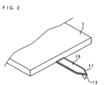
- Fig. 2 is a schematic perspective view showing the AFM probe.
- the needle-shaped body 13 protrudes from the end section of the cantilever 11 provided at one end of the probe holder 1.
- a metal coat 15 is formed on the rear face of the cantilever 11.
- the metal coat 15 is obtained by coating the rear face of the cantilever 11 with aluminum. In other words, the portion where the metal coat 15 is formed is located on the face different from the face on which the needle-shaped body 13 is provided.
- the aluminum constituting the metal coat 15 corresponds to a first metal.
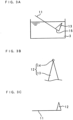
- Figs. 3A, 3B and 3C are schematic views showing a method for manufacturing the probe 12 for tip-enhanced Raman scattering according to Embodiment 1.
- the cantilever 11 from the end section of which the needle-shaped body 13 protrudes, is dipped into an aqueous silver nitrate solution 3.
- the aqueous silver nitrate solution 3 is a solution containing Ag ions.
- the Ag ions contained in the aqueous silver nitrate solution 3 correspond to the ions of a second metal.
- a reducing agent for reducing metal ions is not contained in the aqueous silver nitrate solution 3.
- the cantilever 11 is dipped into the aqueous silver nitrate solution 3 so that the needle-shaped body 13 and at least part of the metal coat 15 formed on the rear face of the cantilever 11 are dipped into the aqueous silver nitrate solution 3. Furthermore, it is desirable that the cantilever 11 should be dipped into the aqueous silver nitrate solution 3 so that the tip end of the needle-shaped body 13 is directed upward. Ag is precipitated and Ag nanostructures are made to grow at the tip end of the needle-shaped body 13 by dipping the cantilever 11 into the aqueous silver nitrate solution 3.
- the Fermi level of the aluminum constituting the metal coat 15 is higher than the Fermi level of Si.
- the electrons inside the aluminum enter the Si constituting the cantilever 11.
- the electrons of the Si pass through the natural oxide film of the Si and flow out into the aqueous silver nitrate solution 3.
- the Ag ions in the aqueous silver nitrate solution 3 are reduced by the electrons having flowed out, and Ag nanostructures are precipitated. Since the electrons are most likely to flow out from the tip end of the needle-shaped body 13, the electrons of the Si mainly flow out from the tip end of the needle-shaped body 13 into the aqueous silver nitrate solution 3.
- the Ag nanostructures are precipitated and made to grow at the tip end of the needle-shaped body 13.
- the electrons are likely to flow out from the tip end of the needle-shaped body 13, and the Ag nanostructures are likely to be precipitated.
- the electrons are more likely to flow out, and the Ag nanostructures are more likely to be precipitated.
- the curvature of the tip end of the needle-shaped body 13 is larger, the electrons are more likely to flow out from the tip end of the needle-shaped body 13.
- the cantilever 11 After the cantilever 11 is dipped into the aqueous silver nitride solution 3 for an appropriate period of time, the cantilever 11 is taken out from the aqueous silver nitride solution 3 and washed. The washing, however, is not essential. As shown in Fig. 3B , the aggregate 14 of the Ag nanostructures is formed at the tip end of the needle-shaped body 13. In addition to the tip end of the needle-shaped body 13, the Ag nanostructures are also precipitated sometimes along the ridge lines of the cantilever 11 including the needle-shaped body 13.
- the size and shape of the aggregate 14 of the Ag nanostructures can be controlled, for example, by adjusting the concentration of the aqueous silver nitride solution 3 or the time during which the cantilever 11 is dipped into the aqueous silver nitride solution 3.
- the probe 12 for tip-enhanced Raman scattering in which the aggregate 14 of the Ag nanostructures is fixed to the tip end of the needle-shaped body 13 protruding from the cantilever 11 is manufactured as described above.
- Fig. 4 is a block diagram showing a configuration of a Raman scattering measurement apparatus.
- the Raman scattering measurement apparatus is equipped with a sample stand 5 on which a sample 2 is placed, the cantilever 11, the probe 12, an irradiation section 61 for applying laser light, and a lens 4 for converging the laser light from the irradiation section 61 to the tip end section of the probe 12 that is brought close to or made contact with the sample 2.
- the probe 12 is provided at the end section of the cantilever 11.
- the sample stand 5 has a sample placement face 51.
- the sample 2 can have any shape such as a flat plate, although the sample 2 having a granular shape is shown in Fig. 4 .
- the Raman scattering measurement apparatus is further equipped with a drive section 66 for moving the cantilever 11, a laser light source 67, an optical sensor 68, a signal processing section 69, and a control section 65.
- the drive section 66 brings the probe 12 close to the sample 2 placed on the sample placement face 51 by moving the cantilever 11.
- the laser light source 67 applies laser light to the rear face of the cantilever 11.
- the laser light is reflected by the metal coat 15 provided on the rear face of the cantilever 11.
- the optical sensor 68 detects the reflected laser light and outputs a signal indicating the result of the detection to the signal processing section 69.
- the laser light is indicated by dashed arrows.
- the cantilever 11 In the case that the tip end section of the probe 12 is brought close to or made contact with the sample 2, the cantilever 11 is bent by an atomic force, the position at which the laser light is detected by the optical sensor 68 is deviated, and the signal processing section 69 detects the bending of the cantilever 11.
- the change in the bending amount of the cantilever 11 corresponds to the change in the distance between the probe 12 and the surface of the sample 2.
- the signal processing section 69 controls the operation of the drive section 66 so that the bending of the cantilever 11 becomes constant.
- the control section 65 controls the operation of the signal processing section 69, thereby controlling the movement of the probe 12.
- the Raman scattering measurement apparatus may be configured to measure the current flowing between the probe 12 and the sample 2 and to control the movement of the probe 12 on the basis of the measured current.
- the Raman scattering measurement apparatus is further equipped with a beam splitter 62, a spectroscope 63, a detection section 64 for detecting light, and a drive section 50 for moving the sample stand 5 in the up-down direction or the left-right direction.
- the laser light applied by the irradiation section 61 passes through the beam splitter 62, is converged by the lens 4, and is applied to the tip end section of the probe 12 that is brought close to or made contact with the sample 2.
- the aggregate 14 of the Ag nanostructures formed at the tip end of the needle-shaped body 13 is included at the tip end section of the probe 12.
- the state of being brought close to is herein the state in which the aggregate 14 of the Ag nanostructures has approached the surface of the sample 2 to the distance to the extent that localized plasmons are induced on the surface of the sample 2 by the applied light, that a locally enhanced electric field is generated, and that tip-enhanced Raman scattering in which Raman scattering light is enhanced is generated.
- Tip-enhanced Raman scattering is generated at the portion on the sample 2 to which the tip end section of the probe 12 is brought close or with which the tip end section of the probe 12 is made contact and to which the laser light is applied.
- the generated Raman scattering light is condensed by the lens 4, is reflected by the beam splitter 62, and enters the spectroscope 63.
- the Raman scattering measurement apparatus is equipped with optical systems composed of numerous optical components, such as mirrors, lenses and filters, for guiding, condensing and separating the laser light and the Raman scattering light.
- optical systems other than the lens 4 and the beam splitter 62 are not shown.
- the spectroscope 63 disperses the incident Raman scattering light.
- the detection section 64 detects the light of various wavelengths dispersed by the spectroscope 63 and outputs signals corresponding to the detection intensity of the light of various wavelengths to the control section 65.
- the control section 65 controls the wavelengths of the light dispersed by the spectroscope 63 and the signals output from the detection section 64 are input to the control section 65, whereby the control section 65 generates a Raman spectrum on the basis of the wavelengths of the dispersed light and the detection intensity of the light indicated by the input signals. In this way, Tip-enhanced Raman scattering is measured.
- the control section 65 controls the operation of the drive section 50 to moves the sample stand 5, thereby making it possible to measure Tip-enhanced Raman scattering at various portions on the sample stand 5.
- the probe 12 in which the aggregate 14 of the Ag nanostructures is fixed to the tip end of the needle-shaped body 13 is manufactured by dipping the cantilever 11, from which the needle-shaped body 13 protrudes and on the rear face of which the metal coat 15 is formed, into the aqueous silver nitride solution 3. Since the Ag nanostructures are precipitated at the tip end of the needle-shaped body 13 by simply dipping the cantilever 11 into the aqueous silver nitride solution 3, the probe 12 for tip-enhanced Raman scattering can be manufactured with little labor without requiring large facilities for vacuum deposition.
- the size and shape of the aggregate 14 of the Ag nanostructures can be controlled by adjusting the concentration of the aqueous silver nitride solution 3 into which the cantilever 11 is dipped or by adjusting the dipping time.
- the size and shape of the aggregate 14 of the Ag nanostructures to be formed on the probe 12 can be controlled freely, whereby it is possible to form the aggregate 14 suited for the wavelengths of the laser light for Raman scattering.
- the probe 12 capable of obtaining the desired degree of enhancement at the time when tip-enhanced Raman scattering is measured can be manufactured by controlling the size and shape of the aggregate 14 of the Ag nanostructures.
- the entire face of the needle-shaped body 13 is not coated with Ag, and the aggregate 14 of the Ag nanostructures is concentratedly formed mainly at the tip end of the needle-shaped body 13.
- the first metal constituting the metal coat 15 may be metals other than aluminum, provided that the metals have Fermi levels higher than that of Si.
- the first metal may be chromium, iron, titanium, zirconium, magnesium, manganese, zinc, nickel, or tin.
- the cantilever 11 including the needle-shaped body 13 may be made of Si having a water resistant film such as a natural oxide film on the surface, or may partially contains Si having no water resistant film.
- the cantilever 11 may also be made of a semiconductor having a water resistant film such as a natural oxide film on the surface, other than Si.
- the first metal is a metal having a Fermi level higher than that of the semiconductor constituting the cantilever 11. What's more, the metal coat 15 made of the first metal may be formed at portions other than the rear face of the cantilever 11.
- the solution containing Ag ions may be solutions other than the aqueous silver nitride solution 3.
- the ions of the second metal contained in the solution into which the cantilever 11 is dipped may be the ions of metals other than Ag. Complex ions are included in the ions of the metal.
- the Fermi level of the solution containing the ions of the second metal or the chemical potential of the electrons in the solution containing the ions of the second metal is preferably lower than the Fermi level of the semiconductor constituting the cantilever 11.
- the Fermi levels referred to in this description respectively indicate Fermi levels before the semiconductor makes contact with a metal or a solution. What's more, although the Fermi level is a term used in semiconductor physics and the chemical potential of the electrons is a term used in solid-state physics and electrochemistry, the Fermi level of the solution containing the ions of the second metal is almost equivalent to the chemical potential of the electrons in the solution containing the ions of the second metal. Alternatively, the Fermi level of the second metal is preferably lower than the Fermi level of the semiconductor constituting the cantilever 11.
- the Fermi level of the solution containing the ions of the second metal should be lower than the Fermi level of the semiconductor constituting the cantilever 11 and that the Fermi level of the second metal should be lower than the Fermi level of the semiconductor constituting the cantilever 11.
- the second metal is, for example, Au (gold), platinum, iridium, palladium, copper or bismuth.
- solutions containing the ions of these metals are used, and the structures of these metals are formed at the tip end of the needle-shaped body 13.
- the probe 12 in which the aggregate of Au nanostructures precipitated at the tip end of the needle-shaped body 13 is manufactured using an aqueous potassium chloroaurate solution. Even in the case that the probe 12 in which the structures of Au, platinum, iridium, palladium, copper or bismuth are precipitated at the tip end of the needle-shaped body 13, tip-enhanced Raman scattering can be measured.
- the structure of the probe 12 is similar to that in Embodiment 1.
- the cantilever 11 is provided at one end of the probe holder 1, and the probe 12 is provided at the end section of the cantilever 11.
- the metal coat 15 is formed on the rear face of the cantilever 11.
- the probe 12 includes the needle-shaped body 13 protruding from the cantilever 11 and the aggregate 14 of metallic structures fixed to the tip end of the needle-shaped body 13.
- the metallic structures in this embodiment are Ag nanostructures.
- the first metal constituting the metal coat 15 is, for example, aluminum.
- the metal coat 15 desirably makes ohmic contact with the cantilever 11.
- the probe 12 is manufactured by dipping the cantilever 11 into a solution containing the ions of the second metal.
- the first metal constituting the metal coat 15 is a metal having an ionization tendency larger than that of the second metal.
- the Fermi level of the first metal in this embodiment may be not more than the Fermi level of the semiconductor constituting the cantilever 11 including the needle-shaped body 13. It is desirable that the cantilever 11 should be made of n-type Si and that the metal coat 15 should make ohmic contact with the cantilever 11.
- the second metal is Ag
- the first metal is aluminum
- the solution containing the ions of the second metal is the aqueous silver nitride solution 3.
- Aluminum has an ionization tendency larger than that of Ag.
- aluminum has a Fermi level lower than that of n-type Si.
- the Fermi level of the first metal is lower than the Fermi level of the semiconductor, the first metal makes Schottky contact with the semiconductor.
- the semiconductor is low-resistance highly doped n-type Si, the first metal makes ohmic contact with the semiconductor due to a quantum-mechanical tunneling phenomenon.
- an AFM probe in which a metal coat made of metal aluminum makes ohmic contact with the cantilever made of n-type Si having a resistance of 0.01 ⁇ cm is commercially available.
- the probe 12 is manufactured by dipping the cantilever 11 into the aqueous silver nitride solution 3.
- the cantilever 11 from the end section of which the needle-shaped body 13 protrudes, is dipped into the aqueous silver nitride solution 3.
- No reducing agent is contained in the aqueous silver nitrate solution 3.
- the cantilever 11 is dipped into the aqueous silver nitrate solution 3 so that the needle-shaped body 13 and at least part of the metal coat 15 are dipped into the aqueous silver nitrate solution 3.
- the ionization tendency of the aluminum constituting the metal coat 15 is larger than the ionization tendency of Ag.
- the aluminum inside the metal coat 15 tends to be oxidized, and the Ag ions inside the aqueous silver nitride solution 3 tend to be reduced.
- the Ag ions When aluminum is oxidized, electrons are emitted from the aluminum.
- the Ag ions When the Ag ions are reduced, the Ag ions absorb electrons. In other words, in the case that the cantilever 11 is dipped into the aqueous silver nitride solution 3, electrons flow from the aluminum inside the metal coat 15 to the Ag ions inside the aqueous silver nitride solution 3.
- the cantilever 11 Since negative carriers are contained in n-type Si, in the case that the cantilever 11 is made of n-type Si, electrons are likely to move inside the cantilever 11 including the needle-shaped body 13. Electrons are likely to flow out from the tip end of the needle-shaped body 13 into the aqueous silver nitride solution 3, and the Ag nanostructures are likely to be precipitated. Hence, the cantilever 11 is desirably made of an n-type semiconductor. What's more, as the curvature of the tip end of the needle-shaped body 13 is larger, electrons are more likely to flow out from the tip end of the needle-shaped body 13.
- the cantilever 11 After the cantilever 11 is dipped into the aqueous silver nitride solution 3 for an appropriate period of time, the cantilever 11 is taken out from the aqueous silver nitride solution 3 and washed. The washing, however, is not essential.
- the aggregate 14 of the Ag nanostructures is formed at the tip end of the needle-shaped body 13.
- the probe 12 in which the aggregate 14 of the Ag nanostructures is fixed to the tip end of the needle-shaped body 13 is manufactured.
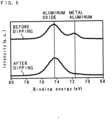
- Fig. 5 is a characteristic graph indicating the analysis result of XPS (X-ray Photoelectron Spectroscopy) for the metal coat 15.
- the horizontal axis represents binding energy
- the vertical axis represents the intensity of photoelectrons.
- the binding energy of aluminum oxide and the binding energy of metal aluminum are indicated by dotted lines.
- Fig. 5 shows the spectrum indicating the result of XPS conducted for the metal coat 15 before the dipping of the cantilever 11 into the aqueous silver nitride solution 3 and the spectrum indicating the result of XPS conducted for the metal coat 15 after the dipping of the cantilever 11 into the aqueous silver nitride solution 3.
- the configuration of the Raman scattering measurement apparatus equipped with the probe 12 is similar to that in Embodiment 1. Also in this embodiment, the Raman scattering measurement apparatus can measure tip-enhanced Raman scattering using the probe 12 in which the aggregate 14 of the Ag nanostructures is fixed to the tip end of the needle-shaped body 13.
- Fig. 6 is a view showing actual examples of the probe 12.
- Fig. 6 shows a plurality of photographs obtained by photographing the tip ends of the needle-shaped bodies 13 of the probes 12 having been manufactured under a plurality of conditions.
- OMCL-AC160TS made by Olympus was used, and each probe 12 was manufactured by dipping the cantilever 11 into the aqueous silver nitride solution 3.
- the aqueous silver nitride solution 3 three kinds of solutions having silver nitrate concentrations of 0.05 mM, 0.1 mM and 1 mM were used. M herein represents mole/L.
- the dipping time during which the cantilever 11 was dipped in the aqueous silver nitride solution 3 was set to two kinds of values, 10 s and 60 s.
- Fig. 6 shows six photographs arranged in two lines and three rows.
- the respective two photographs in the left row, the intermediate row and the right row are photographs obtained by photographing the tip ends of the needle-shaped bodies 13 of the probes 12 having been manufactured at respective silver nitrate concentrations of 0.05 mM, 0.1 mM and 1 mM.
- the respective three photographs in the upper line and the lower line are photographs obtained by photographing the tip ends of the needle-shaped bodies 13 of the probes 12 having been manufactured at respective dipping time values of 10 s and 60 s.
- Each photograph shows the aggregate 14 of the Ag nanostructures. As the concentration of silver nitride is higher and as the dipping time is longer, the size of the aggregate 14 of the Ag nanostructures becomes larger.
- the aggregate 14 of the Ag nanostructures in the probe 12 having been manufactured at a silver nitrate concentration of 0.1 mM and at a dipping time value of 10 s had a size most suitable for measuring tip-enhanced Raman scattering.
- the probe 12 for tip-enhanced Raman scattering can be manufactured with little labor by dipping the cantilever 11, on the rear face of which the metal coat 15 is formed, into the aqueous silver nitride solution 3.
- the size and shape of the aggregate 14 of the Ag nanostructures to be formed on the probe 12 can be controlled freely by adjusting the concentration of the aqueous silver nitride solution 3 into which the cantilever 11 is dipped or by adjusting the dipping time, whereby it is possible to form the aggregate 14 suited for the wavelengths of the laser light for Raman scattering.
- the probe 12 capable of obtaining the desired degree of enhancement at the time when tip-enhanced Raman scattering is measured can be manufactured.
- the solution containing Ag ions may be solutions other than the aqueous silver nitride solution 3.
- the first metal constituting the metal coat 15 may be metals other than aluminum, provided that the ionization tendency of the first metal is larger than the ionization tendency of the second metal, and the ions of the second metal contained in the solution into which the cantilever 11 is dipped may be the ions of metals other than Ag.
- the first metal may be chromium, iron, titanium, zirconium, magnesium, manganese, zinc, nickel, or tin.
- the second metal may be Au (gold), platinum, iridium, palladium, copper, or bismuth.
- the metal coat 15 may be formed at portions other than the rear face of the cantilever 11, provided that the portions are other than the portion positioned at the tip end of the needle-shaped body 13.
- the Fermi level of the solution containing the ions of the second metal is lower than the Fermi level of the semiconductor constituting the cantilever 11 including the needle-shaped body 13. Since the Fermi level of the solution is lower than the Fermi level of the semiconductor, electrons are likely to flow out from the tip end of the needle-shaped body 13 to the solution, and the structures of the second metal are likely to be precipitated.
- the cantilever 11 may be made of semiconductors other than an n-type Si. In the case that the cantilever 11 is made of a p-type semiconductor, the metal coat 15 makes Schottky contact with the cantilever 11. Even in the case that the cantilever 11 is made of a p-type semiconductor or an intrinsic semiconductor, electrons move inside the semiconductor, and the structures of the second metal are precipitated at the tip end of the needle-shaped body 13, whereby the probe 12 is manufactured.
- the probe 12 is manufactured.
- the portion of the cantilever 11 covered with the metal coat 15 includes the tip end of the needle-shaped body 13.
- the ionization tendency of the first metal, such as aluminum, constituting the metal coat 15 is larger than the ionization tendency of the second metal, such as Ag.
- the probe 12 is manufactured.
- the ionization tendency of the first metal is larger than the ionization tendency of the second metal.
- electrons flow out from the cantilever 11 to the solution.
- electrons are likely to flow out from the tip end of the needle-shaped body 13, and as the curvature of the tip end of the needle-shaped body 13 is larger, electrons are more likely to flow out from the tip end of the needle-shaped body 13.
- the structures of the second metal are precipitated at the tip end of the needle-shaped body 13, whereby the probe 12 is manufactured.
- the metal coat 15 is not formed on the cantilever 11, and the probe 12 is provided at the end section of the cantilever 11.
- the probe 12 includes the needle-shaped body 13 protruding from the cantilever 11 and the aggregate 14 of metallic structures fixed to the tip end of the needle-shaped body 13.
- the cantilever 11 including the needle-shaped body 13 is made of an n-type Si.
- the metallic structures in this embodiment are Ag nanostructures.
- the probe 12 is manufactured by dipping the cantilever 11 into the aqueous silver nitride solution 3.
- the Fermi level of the aqueous silver nitride solution 3 is lower than the Fermi level of the n-type Si constituting the cantilever 11.
- the cantilever 11, from the end section of which the needle-shaped body 13 protrudes, is dipped into the aqueous silver nitride solution 3.
- No reducing agent is contained in the aqueous silver nitrate solution 3.
- the cantilever 11 is dipped into the aqueous silver nitride solution 3 so that the needle-shaped body 13 is dipped into the aqueous silver nitride solution 3.
- the cantilever 11 After the cantilever 11 is dipped into the aqueous silver nitride solution 3 for an appropriate period of time, the cantilever 11 is taken out from the aqueous silver nitride solution 3 and washed. The washing, however, is not essential.
- the aggregate 14 of the Ag nanostructures is formed at the tip end of the needle-shaped body 13.
- the probe 12 in which the aggregate 14 of the Ag nanostructures is fixed to the tip end of the needle-shaped body 13 is manufactured although the dipping time is required to be longer than in Embodiments 1 and 2.
- the Raman scattering measurement apparatus can measure tip-enhanced Raman scattering.
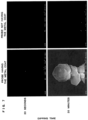
- Fig. 7 is a view showing actual examples of the probe 12 having the metal coat 15 formed on the cantilever 11 and the probe 12 not having the metal coat 15.
- Fig. 7 shows a plurality of photographs obtained by photographing the tip end of the probe 12 manufactured using the cantilever 11 having the metal coat 15 as in Embodiment 2, and by photographing the tip end of the probe 12 manufactured using the cantilever 11 not having the metal coat 15.
- the OMCL-AC160TS made by Olympus was used
- the OMCL-AC160TN made by Olympus was used as the probe holder 1 provided with the cantilever 11 not having the metal coat 15.
- the probes 12 were manufactured by dipping the cantilever 11 into the aqueous silver nitride solution 3.
- the silver nitrate concentration of the aqueous silver nitride solution 3 was set to 0.1 mM.
- the dipping time during which the cantilever 11 was dipped in the aqueous silver nitride solution was set to two kinds of values, 30 seconds and 30 minutes.
- Fig. 7 shows four photographs arranged in two lines and two rows.
- the two photographs in the left row are photographs obtained by photographing the tip ends of the needle-shaped bodies 13 of the probes 12 having been manufactured using the cantilevers 11 having the metal coat 15 formed thereon.
- the two photographs in the right row are photographs obtained by photographing the tip ends of the needle-shaped bodies 13 of the probes 12 having been manufactured using the cantilevers 11 not having the metal coat 15.
- the probes 12 shown in the photographs in the right row are the probes 12 manufactured by the manufacturing method according to this embodiment.
- the respective two photographs in the upper line and the lower line are photographs obtained by photographing the tip ends of the needle-shaped bodies 13 of the probes 12 having been manufactured at dipping time values of 30 seconds and 30 minutes, respectively.
- Each photograph shows the aggregate 14 of the Ag nanostructures.
- the size of the aggregate 14 of the Ag nanostructures is smaller even though the dipping time is the same.
- the aggregate 14 of the Ag nanostructures is made to grow further.
- the probe 12 containing the aggregate 14 of the Ag nanostructures having a sufficiently large size can be manufactured by making the dipping time sufficiently long.
- the probe 12 for tip-enhanced Raman scattering can be manufactured with little labor by dipping the cantilever 11 into the aqueous silver nitride solution 3.
- the size and shape of the aggregate 14 of the Ag nanostructures to be formed on the probe 12 can be controlled freely by adjusting the concentration of the aqueous silver nitride solution 3 into which the cantilever 11 is dipped or by adjusting the dipping time, whereby it is possible to form the aggregate 14 suited for the wavelengths of the laser light for Raman scattering.
- the probe 12 capable of obtaining the desired degree of enhancement at the time when tip-enhanced Raman scattering is measured can be manufactured.
- the solution containing Ag ions may be solutions other than the aqueous silver nitride solution 3.
- the ions of the second metal contained in the solution into which the cantilever 11 is dipped may be ions of metals other than Ag.
- the second metal may be Au (gold), platinum, iridium, palladium, copper, or bismuth.
- the Fermi level of the solution containing the ions of the second metal or the chemical potential of the electrons in the solution containing the ions of the second metal is preferably lower than the Fermi level of the semiconductor constituting the cantilever 11 including the needle-shaped body 13.
- the cantilever 11 may be made of semiconductors other than an n-type Si. Even in the case that the cantilever 11 is made of a p-type semiconductor or an intrinsic semiconductor, thermally excited electrons move inside the semiconductor, the structures of the second metal are precipitated at the tip end of the needle-shaped body 13, whereby the probe 12 is manufactured.
- Figs. 8A, 8B, 8C and 8D are schematic views showing a method for manufacturing the probe 12 according to Embodiment 4 which does not form part of the invention.
- the configuration of the probe 12 to be manufactured by the manufacturing method according to Embodiment 4 is similar to the configuration according to Embodiment 1, 2 or 3.
- the cantilever 11 similar to those according to Embodiments 1 to 3 is dipped into the aqueous silver nitride solution 3. Ag is precipitated at the tip end of the needle-shaped body 13 and the seed of the Ag nanostructures is formed.
- the cantilever 11 is pulled out from the aqueous silver nitride solution 3, and the needle-shaped body 13 is washed and dried as shown in Fig. 8B .
- the cantilever 11 is dipped into the aqueous silver nitride solution 3 again as shown in Fig. 8C .
- the Ag nanostructures are made to grow from the seed of the Ag nanostructures having been formed at the tip end of the needle-shaped body 13.
- the cantilever 11 is taken out from the aqueous silver nitride solution 3.
- the probe 12 for tip-enhanced Raman scattering in which the aggregate 14 of the Ag nanostructures is fixed to the tip end of the needle-shaped body 13 is manufactured as shown in Fig. 8D .
- the configuration of the Raman scattering measurement apparatus equipped with the probe 12 is similar to that in Embodiment 1.
- the probe 12 for tip-enhanced Raman scattering is manufactured by dipping the cantilever 11 into the aqueous silver nitride solution 3, by drying the needle-shaped body 13 once, and by dipping the cantilever 11 into the aqueous silver nitride solution 3 again.
- the aggregate 14 of the Ag nanostructures having a sharper or larger shape is obtained in some cases.
- the aggregate 14 of the Ag nanostructures can be made to grow further, and the probe 12 capable of obtaining the desired degree of enhancement at the time when tip-enhanced Raman scattering is measured can be manufactured.
- the solution containing Ag ions may be solutions other than the aqueous silver nitride solution 3.
- the ions of the second metal contained in the solution into which the cantilever 11 is dipped may be ions of metals other than Ag.
- the second metal may be Au (gold), platinum, iridium, palladium, copper, or bismuth.
- the solution into which the cantilever 11 is dipped first may be different from the solution into which the cantilever 11 is dipped again.
- a manufacturing kit for manufacturing the probe 12 can be used to execute the method for manufacturing the probes 12 according to Embodiments 1 to 4.
- the manufacturing kit includes the cantilever 11 and a solution such as the aqueous silver nitride solution 3 containing the ions of the second metal.
- the cantilever 11 included in the manufacturing kit is provided on the probe holder 1, and the metal coat 15 may be formed on the cantilever 11 or may not be formed.
- the solution included in the manufacturing kit may be used as the raw solution or may be diluted and used.
- the user can manufacture the probe 12 by dipping the cantilever 11 included in the manufacturing kit into the solution included in the manufacturing kit for an appropriate period of time.
- the cantilever 11 may not be included in the manufacturing kit.
- the user can manufacture the probe 12 using, for example, a commercially-available general-purpose cantilever 11 and the solution included in the manufacturing kit.
- the probe 12 having been manufactured by the manufacturing methods according to Embodiments 1 to 4 is used continuously to measure tip-enhanced Raman scattering
- the probe 12 is degraded by the deformation, oxidation or sulfurization of the aggregate 14 of metallic structures fixed to the tip end of the needle-shaped body 13.
- the probe 12 is also degraded in the case that substances other than the aggregate 14 of metallic structures adhere to the aggregate.
- the probe 12 is exposed to the atmosphere, the substances in the atmosphere are adsorbed by the aggregate 14 of metallic structures.
- the probe 12 is also degraded during its storage period.
- the enhancement of Raman scattering light becomes insufficient when tip-enhanced Raman scattering is measured.
- a reconditioned probe 12 is manufactured from a degraded probe 12.
- the probe 12 is reconditioned by removing part of the aggregate 14 of metallic structures from the degraded probe 12, by reducing the aggregate 14 of metallic structures or by removing substances adhered to aggregate 14 of metallic structures.
- the removal of part of the aggregate 14 of metallic structures and the removal of the adhered substances are executed by applying short-wavelength light, such as ultraviolet light, to the tip end of the needle-shaped body 13.
- short-wavelength light such as ultraviolet light
- Part of the aggregate 14 of metallic structures or the substances adhered to the aggregate 14 of metallic structures are removed from the needle-shaped body 13 by applying the short-wavelength light.
- a stripping solution is used to remove part of the aggregate 14 of metallic structures and to remove the adhered substances.
- Part of the aggregate 14 of metallic structures and the substances adhered to the aggregate 14 of metallic structures are removed from the probe 12 by dipping the probe 12 into a stripping solution, such as hydrochloric acid, sulfuric acid, nitric acid, acetic acid, thio nitric acid, etc.
- the degraded probe is reconditioned by removing degraded part of the aggregate 14 of metallic structures.
- the degraded probe is reconditioned by removing the substances adhered to the aggregate 14 of metallic structures.
- a reconditioned probe 12 is manufactured.
- the reconditioned probe 12 may be manufactured by executing any one of the manufacturing methods according to Embodiments 1 to 4 using the cantilever 11 from which part or whole of the aggregate 14 of metallic structures has been removed from the needle-shaped body 13.
- the reduction of the aggregate 14 of the metallic structures is performed by heating or a method in which a reducing agent is used.
- Part of the aggregate 14 of metallic structures is reduced by dipping the probe 12 into a solution in which a reducing agent, such as NaBH 4 , is used as a solute.
- the degraded probe 12 is reconditioned by reducing oxidized part of the aggregate 14 of metallic structures. In this way, the reconditioned probe 12 is manufactured.
- the measurement of tip-enhanced Raman scattering can be made using the manufactured probe 12.
- the probe 12 can be reconditioned so that the desired degree of enhancement is obtained at the time when tip-enhanced Raman scattering is measured.
- the cantilever 11 can be recycled.
- the manufacturing kit for manufacturing the probe 12 can be used to execute the method for manufacturing the probe 12 according to the embodiment.
- the manufacturing kit includes the cantilever 11, a solution such as the aqueous silver nitride solution 3 containing the ions of the second metal, and a reconditioning liquid for reconditioning the probe 12.
- the metal coat 15 may be formed on the cantilever 11, or may not be formed.
- the reconditioning liquid is a stripping solution, such as hydrochloric acid, sulfuric acid, nitric acid, acetic acid, thio nitric acid, etc. or a solution in which a reducing agent, such as NaBH 4 , is used as a solute.
- Each of the solution and the reconditioning liquid included in the manufacturing kit may be used as the raw solution or may be diluted and used.
- the user can manufacture the probe 12 by dipping the cantilever 11 included in the manufacturing kit into the solution included in the manufacturing kit. Furthermore, the user can manufacture a reconditioned probe 12 by dipping a used probe 12 into the reconditioning liquid for an appropriate period of time.
- the cantilever 11 may not be included in the manufacturing kit.
- the solution containing the ions of the second metal is an aqueous solution in Embodiments 1 to 5 described above
- the solution containing the ions of the second metal into which the cantilever 11 is to be dipped may be a solution in which a solvent other than water, such as an organic solvent, is used.
Landscapes
- Chemical & Material Sciences (AREA)
- Health & Medical Sciences (AREA)
- General Health & Medical Sciences (AREA)
- General Physics & Mathematics (AREA)
- Nuclear Medicine, Radiotherapy & Molecular Imaging (AREA)
- Physics & Mathematics (AREA)
- Radiology & Medical Imaging (AREA)
- Immunology (AREA)
- Analytical Chemistry (AREA)
- Biochemistry (AREA)
- Life Sciences & Earth Sciences (AREA)
- Pathology (AREA)
- Chemical Kinetics & Catalysis (AREA)
- General Chemical & Material Sciences (AREA)
- Electrochemistry (AREA)
- Engineering & Computer Science (AREA)
- Materials Engineering (AREA)
- Mechanical Engineering (AREA)
- Metallurgy (AREA)
- Organic Chemistry (AREA)
- Investigating, Analyzing Materials By Fluorescence Or Luminescence (AREA)
- Chemically Coating (AREA)
Claims (7)
- Procédé de fabrication d'une sonde (12) faisant saillie depuis un porte-à-faux (11), comprenant l'étape consistant à :immerger le porte-à-faux (11) constitué d'un semi-conducteur, le porte-à-faux présentant une partie revêtue d'un premier métal et présentant une autre partie non revêtue du premier métal depuis laquelle un corps en forme d'aiguille (13) fait saillie, dans une solution (3) contenant des ions d'un second métal et ne contenant pas d'agent de réduction pour réduire les ions du second métal, pour fabriquer une sonde (12) dans laquelle des structures (14) du second métal sont précipitées sur une extrémité de pointe du corps en forme d'aiguille (13), dans lequelun niveau de Fermi du premier métal est supérieur à un niveau de Fermi du semi-conducteur, etun niveau de Fermi de la solution (3) est inférieur au niveau de Fermi du semi-conducteur.
- Procédé de fabrication d'une sonde (12) faisant saillie depuis un porte-à-faux (11), comprenant l'étape consistant à :immerger le porte-à-faux (11) constitué d'un semi-conducteur, le porte-à-faux présentant une partie revêtue d'un premier métal et présentant une autre partie non revêtue du premier métal depuis laquelle un corps en forme d'aiguille (13) fait saillie, dans une solution (3) contenant des ions d'un second métal et ne contenant pas d'agent de réduction pour réduire les ions du second métal, pour fabriquer une sonde (12) dans laquelle des structures (14) du second métal sont précipitées sur une extrémité de pointe du corps en forme d'aiguille (13), dans lequelun niveau de Fermi du premier métal n'est pas supérieur au niveau de Fermi du semi-conducteur,un niveau de Fermi de la solution (3) est inférieur au niveau de Fermi du semi-conducteur, etle premier métal est un métal présentant une tendance à l'ionisation supérieure à celle du second métal.
- Procédé de fabrication de la sonde (12) selon la revendication 2, dans lequel le revêtement métallique assure un contact ohmique avec le porte-à-faux (11).
- Procédé de fabrication de la sonde (12) selon l'une quelconque des revendications 1 à 3, dans lequel
le premier métal est de l'aluminium, du chrome, du fer, du titane, du zirconium, du magnésium, du manganèse, du zinc, du nickel ou de l'étain. - Procédé de fabrication de la sonde (12) selon l'une quelconque des revendications 1 à 4, dans lequel
après que le porte-à-faux (11) a été immergé dans la solution (3), l'immersion est interrompue, le corps en forme d'aiguille (13) est séché et le porte-à-faux (11) est immergé à nouveau dans la solution (3). - Procédé de fabrication de la sonde (12) selon l'une quelconque des revendications 1 à 5, dans lequel
la solution (3) est une solution (3) contenant des ions d'argent, d'or, de platine, d'iridium, de palladium, de cuivre ou de bismuth. - Procédé de fabrication de la sonde (12) selon l'une quelconque des revendications 1 à 6, comprenant en outre l'étape consistant à :
retirer une partie des structures (14) contenues dans une sonde (12) dégradée, réduire les structures (14) ou retirer des substances adhérant aux structures (14).
Applications Claiming Priority (2)
| Application Number | Priority Date | Filing Date | Title |
|---|---|---|---|
| JP2016130615 | 2016-06-30 | ||
| PCT/JP2017/024240 WO2018003991A1 (fr) | 2016-06-30 | 2017-06-30 | Procédé de fabrication de sonde et sonde |
Publications (3)
| Publication Number | Publication Date |
|---|---|
| EP3480583A1 EP3480583A1 (fr) | 2019-05-08 |
| EP3480583A4 EP3480583A4 (fr) | 2020-02-26 |
| EP3480583B1 true EP3480583B1 (fr) | 2024-04-24 |
Family
ID=60786077
Family Applications (1)
| Application Number | Title | Priority Date | Filing Date |
|---|---|---|---|
| EP17820345.1A Active EP3480583B1 (fr) | 2016-06-30 | 2017-06-30 | Procédé de fabrication de sonde |
Country Status (6)
| Country | Link |
|---|---|
| US (1) | US10900905B2 (fr) |
| EP (1) | EP3480583B1 (fr) |
| JP (1) | JP6989851B2 (fr) |
| KR (1) | KR102581662B1 (fr) |
| CN (1) | CN109416326B (fr) |
| WO (1) | WO2018003991A1 (fr) |
Families Citing this family (6)
| Publication number | Priority date | Publication date | Assignee | Title |
|---|---|---|---|---|
| US10802045B2 (en) * | 2018-03-26 | 2020-10-13 | Bruker Nano, Inc. | Large radius probe |
| KR102101854B1 (ko) * | 2018-09-28 | 2020-04-20 | 전북대학교산학협력단 | 원자간력현미경 팁 및 이의 제조 방법 |
| CN110488045B (zh) * | 2019-09-11 | 2021-09-03 | 重庆医药高等专科学校 | 防脱落型探针装载设备 |
| EP3816637A1 (fr) | 2019-10-31 | 2021-05-05 | ETH Zurich | Procédé de fabrication d'une sonde |
| CN110954714B (zh) * | 2019-12-20 | 2021-10-19 | 江苏集萃微纳自动化系统与装备技术研究所有限公司 | 一种原子力显微镜的探针的刚度实时调节方法 |
| CN111693737B (zh) * | 2020-06-18 | 2021-05-07 | 中国科学院力学研究所 | 一种用于样品表面形貌测量的纳米纤维探针针尖制作方法 |
Family Cites Families (12)
| Publication number | Priority date | Publication date | Assignee | Title |
|---|---|---|---|---|
| JPH09145726A (ja) * | 1995-11-27 | 1997-06-06 | Mitsubishi Electric Corp | 原子間力顕微鏡およびカンチレバーのクリーニング方法 |
| US6002471A (en) | 1996-11-04 | 1999-12-14 | California Institute Of Technology | High resolution scanning raman microscope |
| JP4526626B2 (ja) * | 1999-12-20 | 2010-08-18 | 独立行政法人科学技術振興機構 | 電気特性評価装置 |
| US7335908B2 (en) * | 2002-07-08 | 2008-02-26 | Qunano Ab | Nanostructures and methods for manufacturing the same |
| JP4451252B2 (ja) | 2004-09-02 | 2010-04-14 | エスアイアイ・ナノテクノロジー株式会社 | 近接場顕微鏡用プローブおよびその製造方法ならびにそのプローブを用いた走査型プローブ顕微鏡 |
| JP2006153831A (ja) | 2004-10-27 | 2006-06-15 | Mitsubishi Chemicals Corp | カンチレバーセンサ、センサシステム及び検体液中の検出対象物質の検出方法 |
| JP2008051556A (ja) * | 2006-08-22 | 2008-03-06 | Sii Nanotechnology Inc | 光学式変位検出機構及びそれを用いた表面情報計測装置 |
| JP5256433B2 (ja) | 2007-12-25 | 2013-08-07 | ナノフォトン株式会社 | 散乱型近接場顕微鏡 |
| CN101299457B (zh) | 2008-05-09 | 2010-06-02 | 华南师范大学 | 无汞碱性锌锰和锌银扣式电池负极盖表面处理方法 |
| DE112010002070A5 (de) | 2009-05-22 | 2012-09-13 | Technische Universität Dresden | Vorrichtung und verfahren zur metallisierung von rastersondenspitzen |
| CN103741122A (zh) | 2014-01-20 | 2014-04-23 | 厦门大学 | 一种制备光滑尖锐afm-ters针尖的化学镀方法 |
| JP6065886B2 (ja) | 2014-07-22 | 2017-01-25 | トヨタ自動車株式会社 | 金属皮膜の成膜方法 |
-
2017
- 2017-06-30 CN CN201780038786.8A patent/CN109416326B/zh active Active
- 2017-06-30 US US16/313,761 patent/US10900905B2/en active Active
- 2017-06-30 JP JP2018525309A patent/JP6989851B2/ja active Active
- 2017-06-30 KR KR1020187037543A patent/KR102581662B1/ko active Active
- 2017-06-30 WO PCT/JP2017/024240 patent/WO2018003991A1/fr not_active Ceased
- 2017-06-30 EP EP17820345.1A patent/EP3480583B1/fr active Active
Also Published As
| Publication number | Publication date |
|---|---|
| US10900905B2 (en) | 2021-01-26 |
| CN109416326B (zh) | 2021-12-14 |
| WO2018003991A1 (fr) | 2018-01-04 |
| CN109416326A (zh) | 2019-03-01 |
| EP3480583A1 (fr) | 2019-05-08 |
| EP3480583A4 (fr) | 2020-02-26 |
| US20190170651A1 (en) | 2019-06-06 |
| JPWO2018003991A1 (ja) | 2019-06-13 |
| JP6989851B2 (ja) | 2022-01-12 |
| KR102581662B1 (ko) | 2023-09-22 |
| KR20190024901A (ko) | 2019-03-08 |
Similar Documents
| Publication | Publication Date | Title |
|---|---|---|
| EP3480583B1 (fr) | Procédé de fabrication de sonde | |
| Green et al. | SERS substrates fabricated by island lithography: the silver/pyridine system | |
| Taguchi et al. | Deep‐UV tip‐enhanced Raman scattering | |
| US7450227B2 (en) | Surface enhanced Raman spectroscopy (SERS) substrates exhibiting uniform high enhancement and stability | |
| Galopin et al. | Silicon nanowires coated with silver nanostructures as ultrasensitive interfaces for surface-enhanced Raman spectroscopy | |
| Huang et al. | Rational fabrication of silver-coated AFM TERS tips with a high enhancement and long lifetime | |
| JP4451252B2 (ja) | 近接場顕微鏡用プローブおよびその製造方法ならびにそのプローブを用いた走査型プローブ顕微鏡 | |
| Joshi et al. | based SERS active substrates on demand | |
| PL238322B1 (pl) | Sposób osadzania nanocząstek metalu na powierzchni w procesie elektrochemicznym, powierzchnia otrzymana tym sposobem i jej zastosowanie | |
| JPWO2006106818A1 (ja) | 走査型プローブ顕微鏡用カンチレバー及びそれを具備する走査型プローブ顕微鏡 | |
| Giallongo et al. | Silver nanoparticle arrays on a DVD-derived template: an easy&cheap SERS substrate | |
| JP5256433B2 (ja) | 散乱型近接場顕微鏡 | |
| RU2543691C2 (ru) | Возобновляемая подложка для детектирования поверхностно-усиленного рамановского рассеяния | |
| Yuen et al. | Surface-enhanced raman scattering: Principles, nanostructures, fabrications, and biomedical applications | |
| KR101412420B1 (ko) | 표면증강 라만 산란 센서 및 그 센싱방법 | |
| CN115561224A (zh) | 可循环利用的sers分子检测装置及其使用方法 | |
| Hu et al. | Metal-coated Si nanograss as highly sensitive SERS sensors | |
| Yan et al. | A large-scale SERS substrate fabricated by a grating-like polycarbonate template co-sputtered with AgCu mix-metal | |
| Chacha | Surface enhanced Raman scattering of DNA origami-based bowtie shaped silver nanoparticles | |
| Pavlič | Tip-Enhanced Raman Spectroscopy (TERS) under electrochemical conditions: towards the in situ characterization of functional nanomaterials | |
| WO2023100610A1 (fr) | Procédé de production d'un substrat exalté de surface et spectroscopie exaltée de surface | |
| Murugesan et al. | SERS on Bimetallic Nanostructured thin films | |
| EP2985608A1 (fr) | Pointe protégée pour TERS et son procédé de production | |
| Sai et al. | Comparison of SERS activity of sputtered, electroless-plated and nanoparticle-coated plastic fiber optic probes | |
| Agarwal et al. | Highly Ordered Nanostructures for Ultra-Sensitive SERS |
Legal Events
| Date | Code | Title | Description |
|---|---|---|---|
| STAA | Information on the status of an ep patent application or granted ep patent |
Free format text: STATUS: THE INTERNATIONAL PUBLICATION HAS BEEN MADE |
|
| PUAI | Public reference made under article 153(3) epc to a published international application that has entered the european phase |
Free format text: ORIGINAL CODE: 0009012 |
|
| STAA | Information on the status of an ep patent application or granted ep patent |
Free format text: STATUS: REQUEST FOR EXAMINATION WAS MADE |
|
| 17P | Request for examination filed |
Effective date: 20190115 |
|
| AK | Designated contracting states |
Kind code of ref document: A1 Designated state(s): AL AT BE BG CH CY CZ DE DK EE ES FI FR GB GR HR HU IE IS IT LI LT LU LV MC MK MT NL NO PL PT RO RS SE SI SK SM TR |
|
| AX | Request for extension of the european patent |
Extension state: BA ME |
|
| DAV | Request for validation of the european patent (deleted) | ||
| DAX | Request for extension of the european patent (deleted) | ||
| A4 | Supplementary search report drawn up and despatched |
Effective date: 20200128 |
|
| RIC1 | Information provided on ipc code assigned before grant |
Ipc: G01Q 60/22 20100101ALI20200122BHEP Ipc: G01N 21/65 20060101AFI20200122BHEP Ipc: G01Q 70/18 20100101ALI20200122BHEP Ipc: C23C 18/54 20060101ALI20200122BHEP Ipc: G01Q 70/14 20100101ALI20200122BHEP |
|
| STAA | Information on the status of an ep patent application or granted ep patent |
Free format text: STATUS: EXAMINATION IS IN PROGRESS |
|
| 17Q | First examination report despatched |
Effective date: 20210831 |
|
| GRAP | Despatch of communication of intention to grant a patent |
Free format text: ORIGINAL CODE: EPIDOSNIGR1 |
|
| STAA | Information on the status of an ep patent application or granted ep patent |
Free format text: STATUS: GRANT OF PATENT IS INTENDED |
|
| INTG | Intention to grant announced |
Effective date: 20231201 |
|
| P01 | Opt-out of the competence of the unified patent court (upc) registered |
Effective date: 20240124 |
|
| GRAS | Grant fee paid |
Free format text: ORIGINAL CODE: EPIDOSNIGR3 |
|
| GRAA | (expected) grant |
Free format text: ORIGINAL CODE: 0009210 |
|
| STAA | Information on the status of an ep patent application or granted ep patent |
Free format text: STATUS: THE PATENT HAS BEEN GRANTED |
|
| AK | Designated contracting states |
Kind code of ref document: B1 Designated state(s): AL AT BE BG CH CY CZ DE DK EE ES FI FR GB GR HR HU IE IS IT LI LT LU LV MC MK MT NL NO PL PT RO RS SE SI SK SM TR |
|
| RAP3 | Party data changed (applicant data changed or rights of an application transferred) |
Owner name: HORIBA, LTD. Owner name: KYOTO UNIVERSITY |
|
| REG | Reference to a national code |
Ref country code: GB Ref legal event code: FG4D |
|
| REG | Reference to a national code |
Ref country code: CH Ref legal event code: EP |
|
| REG | Reference to a national code |
Ref country code: DE Ref legal event code: R096 Ref document number: 602017081344 Country of ref document: DE |
|
| REG | Reference to a national code |
Ref country code: IE Ref legal event code: FG4D |
|
| REG | Reference to a national code |
Ref country code: LT Ref legal event code: MG9D |
|
| REG | Reference to a national code |
Ref country code: NL Ref legal event code: MP Effective date: 20240424 |
|
| REG | Reference to a national code |
Ref country code: AT Ref legal event code: MK05 Ref document number: 1680084 Country of ref document: AT Kind code of ref document: T Effective date: 20240424 |
|
| PG25 | Lapsed in a contracting state [announced via postgrant information from national office to epo] |
Ref country code: NL Free format text: LAPSE BECAUSE OF FAILURE TO SUBMIT A TRANSLATION OF THE DESCRIPTION OR TO PAY THE FEE WITHIN THE PRESCRIBED TIME-LIMIT Effective date: 20240424 |
|
| PG25 | Lapsed in a contracting state [announced via postgrant information from national office to epo] |
Ref country code: NL Free format text: LAPSE BECAUSE OF FAILURE TO SUBMIT A TRANSLATION OF THE DESCRIPTION OR TO PAY THE FEE WITHIN THE PRESCRIBED TIME-LIMIT Effective date: 20240424 |
|
| PG25 | Lapsed in a contracting state [announced via postgrant information from national office to epo] |
Ref country code: IS Free format text: LAPSE BECAUSE OF FAILURE TO SUBMIT A TRANSLATION OF THE DESCRIPTION OR TO PAY THE FEE WITHIN THE PRESCRIBED TIME-LIMIT Effective date: 20240824 |
|
| PG25 | Lapsed in a contracting state [announced via postgrant information from national office to epo] |
Ref country code: BG Free format text: LAPSE BECAUSE OF FAILURE TO SUBMIT A TRANSLATION OF THE DESCRIPTION OR TO PAY THE FEE WITHIN THE PRESCRIBED TIME-LIMIT Effective date: 20240424 |
|
| PG25 | Lapsed in a contracting state [announced via postgrant information from national office to epo] |
Ref country code: HR Free format text: LAPSE BECAUSE OF FAILURE TO SUBMIT A TRANSLATION OF THE DESCRIPTION OR TO PAY THE FEE WITHIN THE PRESCRIBED TIME-LIMIT Effective date: 20240424 Ref country code: FI Free format text: LAPSE BECAUSE OF FAILURE TO SUBMIT A TRANSLATION OF THE DESCRIPTION OR TO PAY THE FEE WITHIN THE PRESCRIBED TIME-LIMIT Effective date: 20240424 |
|
| PG25 | Lapsed in a contracting state [announced via postgrant information from national office to epo] |
Ref country code: GR Free format text: LAPSE BECAUSE OF FAILURE TO SUBMIT A TRANSLATION OF THE DESCRIPTION OR TO PAY THE FEE WITHIN THE PRESCRIBED TIME-LIMIT Effective date: 20240725 |
|
| PG25 | Lapsed in a contracting state [announced via postgrant information from national office to epo] |
Ref country code: PT Free format text: LAPSE BECAUSE OF FAILURE TO SUBMIT A TRANSLATION OF THE DESCRIPTION OR TO PAY THE FEE WITHIN THE PRESCRIBED TIME-LIMIT Effective date: 20240826 |
|
| PG25 | Lapsed in a contracting state [announced via postgrant information from national office to epo] |
Ref country code: ES Free format text: LAPSE BECAUSE OF FAILURE TO SUBMIT A TRANSLATION OF THE DESCRIPTION OR TO PAY THE FEE WITHIN THE PRESCRIBED TIME-LIMIT Effective date: 20240424 |
|
| PG25 | Lapsed in a contracting state [announced via postgrant information from national office to epo] |
Ref country code: AT Free format text: LAPSE BECAUSE OF FAILURE TO SUBMIT A TRANSLATION OF THE DESCRIPTION OR TO PAY THE FEE WITHIN THE PRESCRIBED TIME-LIMIT Effective date: 20240424 |
|
| PG25 | Lapsed in a contracting state [announced via postgrant information from national office to epo] |
Ref country code: PL Free format text: LAPSE BECAUSE OF FAILURE TO SUBMIT A TRANSLATION OF THE DESCRIPTION OR TO PAY THE FEE WITHIN THE PRESCRIBED TIME-LIMIT Effective date: 20240424 |
|
| PG25 | Lapsed in a contracting state [announced via postgrant information from national office to epo] |
Ref country code: LV Free format text: LAPSE BECAUSE OF FAILURE TO SUBMIT A TRANSLATION OF THE DESCRIPTION OR TO PAY THE FEE WITHIN THE PRESCRIBED TIME-LIMIT Effective date: 20240424 |
|
| PG25 | Lapsed in a contracting state [announced via postgrant information from national office to epo] |
Ref country code: PT Free format text: LAPSE BECAUSE OF FAILURE TO SUBMIT A TRANSLATION OF THE DESCRIPTION OR TO PAY THE FEE WITHIN THE PRESCRIBED TIME-LIMIT Effective date: 20240826 Ref country code: PL Free format text: LAPSE BECAUSE OF FAILURE TO SUBMIT A TRANSLATION OF THE DESCRIPTION OR TO PAY THE FEE WITHIN THE PRESCRIBED TIME-LIMIT Effective date: 20240424 Ref country code: NO Free format text: LAPSE BECAUSE OF FAILURE TO SUBMIT A TRANSLATION OF THE DESCRIPTION OR TO PAY THE FEE WITHIN THE PRESCRIBED TIME-LIMIT Effective date: 20240724 Ref country code: LV Free format text: LAPSE BECAUSE OF FAILURE TO SUBMIT A TRANSLATION OF THE DESCRIPTION OR TO PAY THE FEE WITHIN THE PRESCRIBED TIME-LIMIT Effective date: 20240424 Ref country code: IS Free format text: LAPSE BECAUSE OF FAILURE TO SUBMIT A TRANSLATION OF THE DESCRIPTION OR TO PAY THE FEE WITHIN THE PRESCRIBED TIME-LIMIT Effective date: 20240824 Ref country code: HR Free format text: LAPSE BECAUSE OF FAILURE TO SUBMIT A TRANSLATION OF THE DESCRIPTION OR TO PAY THE FEE WITHIN THE PRESCRIBED TIME-LIMIT Effective date: 20240424 Ref country code: GR Free format text: LAPSE BECAUSE OF FAILURE TO SUBMIT A TRANSLATION OF THE DESCRIPTION OR TO PAY THE FEE WITHIN THE PRESCRIBED TIME-LIMIT Effective date: 20240725 Ref country code: FI Free format text: LAPSE BECAUSE OF FAILURE TO SUBMIT A TRANSLATION OF THE DESCRIPTION OR TO PAY THE FEE WITHIN THE PRESCRIBED TIME-LIMIT Effective date: 20240424 Ref country code: ES Free format text: LAPSE BECAUSE OF FAILURE TO SUBMIT A TRANSLATION OF THE DESCRIPTION OR TO PAY THE FEE WITHIN THE PRESCRIBED TIME-LIMIT Effective date: 20240424 Ref country code: BG Free format text: LAPSE BECAUSE OF FAILURE TO SUBMIT A TRANSLATION OF THE DESCRIPTION OR TO PAY THE FEE WITHIN THE PRESCRIBED TIME-LIMIT Effective date: 20240424 Ref country code: AT Free format text: LAPSE BECAUSE OF FAILURE TO SUBMIT A TRANSLATION OF THE DESCRIPTION OR TO PAY THE FEE WITHIN THE PRESCRIBED TIME-LIMIT Effective date: 20240424 Ref country code: RS Free format text: LAPSE BECAUSE OF FAILURE TO SUBMIT A TRANSLATION OF THE DESCRIPTION OR TO PAY THE FEE WITHIN THE PRESCRIBED TIME-LIMIT Effective date: 20240724 |
|
| PG25 | Lapsed in a contracting state [announced via postgrant information from national office to epo] |
Ref country code: DK Free format text: LAPSE BECAUSE OF FAILURE TO SUBMIT A TRANSLATION OF THE DESCRIPTION OR TO PAY THE FEE WITHIN THE PRESCRIBED TIME-LIMIT Effective date: 20240424 |
|
| PG25 | Lapsed in a contracting state [announced via postgrant information from national office to epo] |
Ref country code: EE Free format text: LAPSE BECAUSE OF FAILURE TO SUBMIT A TRANSLATION OF THE DESCRIPTION OR TO PAY THE FEE WITHIN THE PRESCRIBED TIME-LIMIT Effective date: 20240424 |
|
| PG25 | Lapsed in a contracting state [announced via postgrant information from national office to epo] |
Ref country code: CZ Free format text: LAPSE BECAUSE OF FAILURE TO SUBMIT A TRANSLATION OF THE DESCRIPTION OR TO PAY THE FEE WITHIN THE PRESCRIBED TIME-LIMIT Effective date: 20240424 |
|
| PG25 | Lapsed in a contracting state [announced via postgrant information from national office to epo] |
Ref country code: RO Free format text: LAPSE BECAUSE OF FAILURE TO SUBMIT A TRANSLATION OF THE DESCRIPTION OR TO PAY THE FEE WITHIN THE PRESCRIBED TIME-LIMIT Effective date: 20240424 Ref country code: SK Free format text: LAPSE BECAUSE OF FAILURE TO SUBMIT A TRANSLATION OF THE DESCRIPTION OR TO PAY THE FEE WITHIN THE PRESCRIBED TIME-LIMIT Effective date: 20240424 |
|
| REG | Reference to a national code |
Ref country code: DE Ref legal event code: R097 Ref document number: 602017081344 Country of ref document: DE |
|
| PG25 | Lapsed in a contracting state [announced via postgrant information from national office to epo] |
Ref country code: SM Free format text: LAPSE BECAUSE OF FAILURE TO SUBMIT A TRANSLATION OF THE DESCRIPTION OR TO PAY THE FEE WITHIN THE PRESCRIBED TIME-LIMIT Effective date: 20240424 |
|
| PG25 | Lapsed in a contracting state [announced via postgrant information from national office to epo] |
Ref country code: SM Free format text: LAPSE BECAUSE OF FAILURE TO SUBMIT A TRANSLATION OF THE DESCRIPTION OR TO PAY THE FEE WITHIN THE PRESCRIBED TIME-LIMIT Effective date: 20240424 Ref country code: SK Free format text: LAPSE BECAUSE OF FAILURE TO SUBMIT A TRANSLATION OF THE DESCRIPTION OR TO PAY THE FEE WITHIN THE PRESCRIBED TIME-LIMIT Effective date: 20240424 Ref country code: RO Free format text: LAPSE BECAUSE OF FAILURE TO SUBMIT A TRANSLATION OF THE DESCRIPTION OR TO PAY THE FEE WITHIN THE PRESCRIBED TIME-LIMIT Effective date: 20240424 Ref country code: EE Free format text: LAPSE BECAUSE OF FAILURE TO SUBMIT A TRANSLATION OF THE DESCRIPTION OR TO PAY THE FEE WITHIN THE PRESCRIBED TIME-LIMIT Effective date: 20240424 Ref country code: DK Free format text: LAPSE BECAUSE OF FAILURE TO SUBMIT A TRANSLATION OF THE DESCRIPTION OR TO PAY THE FEE WITHIN THE PRESCRIBED TIME-LIMIT Effective date: 20240424 Ref country code: CZ Free format text: LAPSE BECAUSE OF FAILURE TO SUBMIT A TRANSLATION OF THE DESCRIPTION OR TO PAY THE FEE WITHIN THE PRESCRIBED TIME-LIMIT Effective date: 20240424 Ref country code: MC Free format text: LAPSE BECAUSE OF FAILURE TO SUBMIT A TRANSLATION OF THE DESCRIPTION OR TO PAY THE FEE WITHIN THE PRESCRIBED TIME-LIMIT Effective date: 20240424 |
|
| REG | Reference to a national code |
Ref country code: CH Ref legal event code: PL |
|
| PG25 | Lapsed in a contracting state [announced via postgrant information from national office to epo] |
Ref country code: LU Free format text: LAPSE BECAUSE OF NON-PAYMENT OF DUE FEES Effective date: 20240630 |
|
| PLBE | No opposition filed within time limit |
Free format text: ORIGINAL CODE: 0009261 |
|
| STAA | Information on the status of an ep patent application or granted ep patent |
Free format text: STATUS: NO OPPOSITION FILED WITHIN TIME LIMIT |
|
| 26N | No opposition filed |
Effective date: 20250127 |
|
| PG25 | Lapsed in a contracting state [announced via postgrant information from national office to epo] |
Ref country code: IE Free format text: LAPSE BECAUSE OF NON-PAYMENT OF DUE FEES Effective date: 20240630 |
|
| PG25 | Lapsed in a contracting state [announced via postgrant information from national office to epo] |
Ref country code: SI Free format text: LAPSE BECAUSE OF FAILURE TO SUBMIT A TRANSLATION OF THE DESCRIPTION OR TO PAY THE FEE WITHIN THE PRESCRIBED TIME-LIMIT Effective date: 20240424 Ref country code: CH Free format text: LAPSE BECAUSE OF NON-PAYMENT OF DUE FEES Effective date: 20240630 Ref country code: BE Free format text: LAPSE BECAUSE OF NON-PAYMENT OF DUE FEES Effective date: 20240630 |
|
| REG | Reference to a national code |
Ref country code: BE Ref legal event code: MM Effective date: 20240630 |
|
| PGFP | Annual fee paid to national office [announced via postgrant information from national office to epo] |
Ref country code: GB Payment date: 20250618 Year of fee payment: 9 |
|
| PGFP | Annual fee paid to national office [announced via postgrant information from national office to epo] |
Ref country code: FR Payment date: 20250625 Year of fee payment: 9 |
|
| PG25 | Lapsed in a contracting state [announced via postgrant information from national office to epo] |
Ref country code: SE Free format text: LAPSE BECAUSE OF FAILURE TO SUBMIT A TRANSLATION OF THE DESCRIPTION OR TO PAY THE FEE WITHIN THE PRESCRIBED TIME-LIMIT Effective date: 20240424 |
|
| PGFP | Annual fee paid to national office [announced via postgrant information from national office to epo] |
Ref country code: DE Payment date: 20250630 Year of fee payment: 9 |
|
| PG25 | Lapsed in a contracting state [announced via postgrant information from national office to epo] |
Ref country code: CY Free format text: LAPSE BECAUSE OF FAILURE TO SUBMIT A TRANSLATION OF THE DESCRIPTION OR TO PAY THE FEE WITHIN THE PRESCRIBED TIME-LIMIT; INVALID AB INITIO Effective date: 20170630 |
|
| PG25 | Lapsed in a contracting state [announced via postgrant information from national office to epo] |
Ref country code: IT Free format text: LAPSE BECAUSE OF FAILURE TO SUBMIT A TRANSLATION OF THE DESCRIPTION OR TO PAY THE FEE WITHIN THE PRESCRIBED TIME-LIMIT Effective date: 20240424 |
|
| PG25 | Lapsed in a contracting state [announced via postgrant information from national office to epo] |
Ref country code: HU Free format text: LAPSE BECAUSE OF FAILURE TO SUBMIT A TRANSLATION OF THE DESCRIPTION OR TO PAY THE FEE WITHIN THE PRESCRIBED TIME-LIMIT; INVALID AB INITIO Effective date: 20170630 |