EP3480846B1 - Halbleiteranordnung mit zuverlässig schaltenden steuerbaren halbleiterelementen - Google Patents
Halbleiteranordnung mit zuverlässig schaltenden steuerbaren halbleiterelementen Download PDFInfo
- Publication number
- EP3480846B1 EP3480846B1 EP17199950.1A EP17199950A EP3480846B1 EP 3480846 B1 EP3480846 B1 EP 3480846B1 EP 17199950 A EP17199950 A EP 17199950A EP 3480846 B1 EP3480846 B1 EP 3480846B1
- Authority
- EP
- European Patent Office
- Prior art keywords
- conductor track
- section
- semiconductor chips
- subset
- semiconductor
- Prior art date
- Legal status (The legal status is an assumption and is not a legal conclusion. Google has not performed a legal analysis and makes no representation as to the accuracy of the status listed.)
- Active
Links
Images


Classifications
-
- H—ELECTRICITY
- H10—SEMICONDUCTOR DEVICES; ELECTRIC SOLID-STATE DEVICES NOT OTHERWISE PROVIDED FOR
- H10W—GENERIC PACKAGES, INTERCONNECTIONS, CONNECTORS OR OTHER CONSTRUCTIONAL DETAILS OF DEVICES COVERED BY CLASS H10
- H10W70/00—Package substrates; Interposers; Redistribution layers [RDL]
- H10W70/60—Insulating or insulated package substrates; Interposers; Redistribution layers
- H10W70/62—Insulating or insulated package substrates; Interposers; Redistribution layers characterised by their interconnections
- H10W70/65—Shapes or dispositions of interconnections
- H10W70/658—Shapes or dispositions of interconnections for devices provided for in groups H10D8/00 - H10D48/00
-
- H—ELECTRICITY
- H10—SEMICONDUCTOR DEVICES; ELECTRIC SOLID-STATE DEVICES NOT OTHERWISE PROVIDED FOR
- H10W—GENERIC PACKAGES, INTERCONNECTIONS, CONNECTORS OR OTHER CONSTRUCTIONAL DETAILS OF DEVICES COVERED BY CLASS H10
- H10W70/00—Package substrates; Interposers; Redistribution layers [RDL]
- H10W70/60—Insulating or insulated package substrates; Interposers; Redistribution layers
- H10W70/611—Insulating or insulated package substrates; Interposers; Redistribution layers for connecting multiple chips together
-
- H—ELECTRICITY
- H10—SEMICONDUCTOR DEVICES; ELECTRIC SOLID-STATE DEVICES NOT OTHERWISE PROVIDED FOR
- H10W—GENERIC PACKAGES, INTERCONNECTIONS, CONNECTORS OR OTHER CONSTRUCTIONAL DETAILS OF DEVICES COVERED BY CLASS H10
- H10W70/00—Package substrates; Interposers; Redistribution layers [RDL]
- H10W70/60—Insulating or insulated package substrates; Interposers; Redistribution layers
- H10W70/62—Insulating or insulated package substrates; Interposers; Redistribution layers characterised by their interconnections
- H10W70/65—Shapes or dispositions of interconnections
-
- H—ELECTRICITY
- H10—SEMICONDUCTOR DEVICES; ELECTRIC SOLID-STATE DEVICES NOT OTHERWISE PROVIDED FOR
- H10W—GENERIC PACKAGES, INTERCONNECTIONS, CONNECTORS OR OTHER CONSTRUCTIONAL DETAILS OF DEVICES COVERED BY CLASS H10
- H10W90/00—Package configurations
-
- H—ELECTRICITY
- H10—SEMICONDUCTOR DEVICES; ELECTRIC SOLID-STATE DEVICES NOT OTHERWISE PROVIDED FOR
- H10W—GENERIC PACKAGES, INTERCONNECTIONS, CONNECTORS OR OTHER CONSTRUCTIONAL DETAILS OF DEVICES COVERED BY CLASS H10
- H10W90/00—Package configurations
- H10W90/701—Package configurations characterised by the relative positions of pads or connectors relative to package parts
-
- H—ELECTRICITY
- H10—SEMICONDUCTOR DEVICES; ELECTRIC SOLID-STATE DEVICES NOT OTHERWISE PROVIDED FOR
- H10W—GENERIC PACKAGES, INTERCONNECTIONS, CONNECTORS OR OTHER CONSTRUCTIONAL DETAILS OF DEVICES COVERED BY CLASS H10
- H10W40/00—Arrangements for thermal protection or thermal control
- H10W40/20—Arrangements for cooling
- H10W40/25—Arrangements for cooling characterised by their materials
- H10W40/255—Arrangements for cooling characterised by their materials having a laminate or multilayered structure, e.g. direct bond copper [DBC] ceramic substrates
-
- H—ELECTRICITY
- H10—SEMICONDUCTOR DEVICES; ELECTRIC SOLID-STATE DEVICES NOT OTHERWISE PROVIDED FOR
- H10W—GENERIC PACKAGES, INTERCONNECTIONS, CONNECTORS OR OTHER CONSTRUCTIONAL DETAILS OF DEVICES COVERED BY CLASS H10
- H10W72/00—Interconnections or connectors in packages
- H10W72/071—Connecting or disconnecting
- H10W72/075—Connecting or disconnecting of bond wires
- H10W72/07551—Connecting or disconnecting of bond wires characterised by changes in properties of the bond wires during the connecting
- H10W72/07552—Connecting or disconnecting of bond wires characterised by changes in properties of the bond wires during the connecting changes in structures or sizes
-
- H—ELECTRICITY
- H10—SEMICONDUCTOR DEVICES; ELECTRIC SOLID-STATE DEVICES NOT OTHERWISE PROVIDED FOR
- H10W—GENERIC PACKAGES, INTERCONNECTIONS, CONNECTORS OR OTHER CONSTRUCTIONAL DETAILS OF DEVICES COVERED BY CLASS H10
- H10W72/00—Interconnections or connectors in packages
- H10W72/50—Bond wires
- H10W72/521—Structures or relative sizes of bond wires
- H10W72/527—Multiple bond wires having different sizes
-
- H—ELECTRICITY
- H10—SEMICONDUCTOR DEVICES; ELECTRIC SOLID-STATE DEVICES NOT OTHERWISE PROVIDED FOR
- H10W—GENERIC PACKAGES, INTERCONNECTIONS, CONNECTORS OR OTHER CONSTRUCTIONAL DETAILS OF DEVICES COVERED BY CLASS H10
- H10W72/00—Interconnections or connectors in packages
- H10W72/50—Bond wires
- H10W72/531—Shapes of wire connectors
- H10W72/533—Cross-sectional shape
- H10W72/534—Cross-sectional shape being rectangular
-
- H—ELECTRICITY
- H10—SEMICONDUCTOR DEVICES; ELECTRIC SOLID-STATE DEVICES NOT OTHERWISE PROVIDED FOR
- H10W—GENERIC PACKAGES, INTERCONNECTIONS, CONNECTORS OR OTHER CONSTRUCTIONAL DETAILS OF DEVICES COVERED BY CLASS H10
- H10W72/00—Interconnections or connectors in packages
- H10W72/50—Bond wires
- H10W72/541—Dispositions of bond wires
- H10W72/5445—Dispositions of bond wires being orthogonal to a side surface of the chip, e.g. parallel arrangements
-
- H—ELECTRICITY
- H10—SEMICONDUCTOR DEVICES; ELECTRIC SOLID-STATE DEVICES NOT OTHERWISE PROVIDED FOR
- H10W—GENERIC PACKAGES, INTERCONNECTIONS, CONNECTORS OR OTHER CONSTRUCTIONAL DETAILS OF DEVICES COVERED BY CLASS H10
- H10W72/00—Interconnections or connectors in packages
- H10W72/50—Bond wires
- H10W72/541—Dispositions of bond wires
- H10W72/547—Dispositions of multiple bond wires
- H10W72/5475—Dispositions of multiple bond wires multiple bond wires connected to common bond pads at both ends of the wires
-
- H—ELECTRICITY
- H10—SEMICONDUCTOR DEVICES; ELECTRIC SOLID-STATE DEVICES NOT OTHERWISE PROVIDED FOR
- H10W—GENERIC PACKAGES, INTERCONNECTIONS, CONNECTORS OR OTHER CONSTRUCTIONAL DETAILS OF DEVICES COVERED BY CLASS H10
- H10W72/00—Interconnections or connectors in packages
- H10W72/851—Dispositions of multiple connectors or interconnections
- H10W72/874—On different surfaces
- H10W72/884—Die-attach connectors and bond wires
-
- H—ELECTRICITY
- H10—SEMICONDUCTOR DEVICES; ELECTRIC SOLID-STATE DEVICES NOT OTHERWISE PROVIDED FOR
- H10W—GENERIC PACKAGES, INTERCONNECTIONS, CONNECTORS OR OTHER CONSTRUCTIONAL DETAILS OF DEVICES COVERED BY CLASS H10
- H10W72/00—Interconnections or connectors in packages
- H10W72/90—Bond pads, in general
- H10W72/921—Structures or relative sizes of bond pads
- H10W72/926—Multiple bond pads having different sizes
-
- H—ELECTRICITY
- H10—SEMICONDUCTOR DEVICES; ELECTRIC SOLID-STATE DEVICES NOT OTHERWISE PROVIDED FOR
- H10W—GENERIC PACKAGES, INTERCONNECTIONS, CONNECTORS OR OTHER CONSTRUCTIONAL DETAILS OF DEVICES COVERED BY CLASS H10
- H10W90/00—Package configurations
- H10W90/701—Package configurations characterised by the relative positions of pads or connectors relative to package parts
- H10W90/731—Package configurations characterised by the relative positions of pads or connectors relative to package parts of die-attach connectors
- H10W90/734—Package configurations characterised by the relative positions of pads or connectors relative to package parts of die-attach connectors between a chip and a stacked insulating package substrate, interposer or RDL
-
- H—ELECTRICITY
- H10—SEMICONDUCTOR DEVICES; ELECTRIC SOLID-STATE DEVICES NOT OTHERWISE PROVIDED FOR
- H10W—GENERIC PACKAGES, INTERCONNECTIONS, CONNECTORS OR OTHER CONSTRUCTIONAL DETAILS OF DEVICES COVERED BY CLASS H10
- H10W90/00—Package configurations
- H10W90/701—Package configurations characterised by the relative positions of pads or connectors relative to package parts
- H10W90/751—Package configurations characterised by the relative positions of pads or connectors relative to package parts of bond wires
- H10W90/753—Package configurations characterised by the relative positions of pads or connectors relative to package parts of bond wires between laterally-adjacent chips
-
- H—ELECTRICITY
- H10—SEMICONDUCTOR DEVICES; ELECTRIC SOLID-STATE DEVICES NOT OTHERWISE PROVIDED FOR
- H10W—GENERIC PACKAGES, INTERCONNECTIONS, CONNECTORS OR OTHER CONSTRUCTIONAL DETAILS OF DEVICES COVERED BY CLASS H10
- H10W90/00—Package configurations
- H10W90/701—Package configurations characterised by the relative positions of pads or connectors relative to package parts
- H10W90/751—Package configurations characterised by the relative positions of pads or connectors relative to package parts of bond wires
- H10W90/754—Package configurations characterised by the relative positions of pads or connectors relative to package parts of bond wires between a chip and a stacked insulating package substrate, interposer or RDL
Definitions
- the instant disclosure relates to semiconductor arrangements having controllable semiconductor elements.
- Such a semiconductor arrangement includes at least one controllable semiconductor element, each having a first load electrode, a second load electrode, a load path formed therebetween, and a control electrode for controlling the load path.
- the arrangement may include two or more controllable semiconductor elements electrically connected in parallel such that their load paths are electrically connected in parallel, e.g. by electrically connecting the first load electrodes to one another, and by electrically connecting the second load electrodes to one another.
- the control electrodes may be electrically connected to one another.
- the two or more controllable semiconductor elements electrically connected in parallel are operated synchronously by feeding a common control voltage (e.g. provided by a controller) to the individual controllable semiconductor elements using electrical lines.
- the switching state of a controllable semiconductor element e.g. whether the load path is electrically conducting or blocking, depends on its individual control voltage, i.e. on the difference between the electric potential of the control electrode and, e.g., the first load electrode of the corresponding controllable semiconductor element
- a large current flowing through a line electrically connecting the first load electrodes can, in combination with the inevitable ohmic resistance and/or inductance of that line, lead to significantly different electric potentials at the first load electrodes of the different controllable semiconductor elements. Therefore, there may be situations in which the switching states of different controllable semiconductor elements significantly differ from each other.
- the described problems are, without being restricted to, of particular interest with regard to fast switching semiconductor elements like semiconductor elements based on silicon carbide (e.g. SiC-based MOSFETs or SiC-based IGBTs) because the silicon-carbide-based semiconductor chips presently available have small foot print areas and, therefore, low rated currents so that there is a frequent requirement of electrically connecting silicon-carbide-based semiconductor chips in parallel.
- silicon carbide e.g. SiC-based MOSFETs or SiC-based IGBTs
- Document EP 0 533 158 A2 discloses an inverter device including plural modules, each module being formed by a series circuit having a parallel circuit of a first switching device and a first diode, and a parallel circuit of a second switching device and a second diode, allowing a reduced size, high reliability, high frequency switching and low noise.
- Document US 2016/0056132 A1 discloses a circuit arrangement including at least two semiconductor chip having first and second load terminals that are each connected to one another, a first load current collecting conductor track, and also an external terminal electrically conductively connected thereto.
- first and second load terminals that are each connected to one another, a first load current collecting conductor track, and also an external terminal electrically conductively connected thereto.
- For each of the semiconductor chips there is at least one electrical connection conductor electrically conductively connected to the first load terminal of the relevant semiconductor chip and also to the first load current collecting conductor track.
- the total inductance of all the connection conductors with which the first load terminal of the second of the semiconductor chips is connected to the first load current collecting conductor track has at least twice the inductance of that section of the first load current collecting conductor track which is formed between the second connection location of the first of the semiconductor chips and the second connection location of the second of the semiconductor chips.
- the present invention is directed to a semiconductor arrangement according to claim 1.
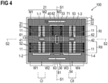
- Figure 1 is a top view illustrating a semiconductor arrangement 100
- Figure 2 is a cross-sectional view of the semiconductor arrangement of Figure 1 in a cross-sectional plane E1-E1
- Figure 3 is an electronic symbol of a controllable semiconductor element comprising a MOSFET.
- the semiconductor arrangement 100 includes a circuit board 2 and a multiplicity (here: eight) of semiconductor chips 1 arranged on the circuit board 2.
- Each of the semiconductor chips 1 comprises a semiconductor body 10, and each semiconductor body 10 (and, therefore, each of the semiconductor chips 1) comprises a controllable semiconductor element T.
- Each semiconductor chip 1 includes, in addition to the semiconductor body 10, a first load electrode 11 arranged on the semiconductor body 10, a second load electrode 12 arranged on the semiconductor body 10, and a control electrode 13 arranged on the semiconductor body 10.
- the first load electrode 11 and the control electrode 13 may be arranged on that surface of the semiconductor body 10 facing away from the circuit board 2
- the second load electrode 12 may be arranged on that surface of the semiconductor body 10 facing towards the circuit board 2.
- Each of the controllable semiconductor elements T includes a load path integrated in the semiconductor body 10 between the first and second load electrodes 11, 12 of the respective controllable semiconductor element T.
- a control voltage may be applied between the control electrode 13 and one of the first or second load electrodes 11, 12.
- the semiconductor body 10 of each of the semiconductor chips 1 includes an individual controllable semiconductor element T.
- Different controllable semiconductor elements T may be identical to each other. In this sense, “identical” may mean identical "apart from fabrication tolerances".
- suitable controllable semiconductor elements T include, without being restricted to, unipolar or bipolar transistors, thyristors, or any other controllable semiconductor elements.
- the controllable semiconductor elements T comprise transistors
- the identical controllable semiconductor elements T may comprise, e.g., IGFETs (Insulated Gate Field Effect Transistors) like MOSFETs (Metal Oxide Semiconductor Field-Effect Transistors) or IGBTs (Insulated Gate Bipolar Transistors; e.g.
- the first load electrode 11 and the second load electrode 12 may be a source electrode and a drain electrode, or a drain electrode and a source electrode, an emitter electrode and a collector electrode, or a collector electrode and an emitter electrode, and the control electrode 13 may be a gate electrode or a base electrode.
- the principles of design and operation of such semiconductor elements T are known in the art so that no further explanations are required in this regard.
- FIG 3 illustrates an electronic symbol of an exemplary controllable semiconductor element T comprising a MOSFET.
- a semiconductor chip 1 that includes a controllable semiconductor element T may optionally also include an integrated diode 14 which may, depending on the application, operate as freewheeling diode.
- the controllable semiconductor element T comprises a MOSFET, it may include an inherent body diode which forms the integrated diode 14.
- the controllable semiconductor element T comprises an RC-IGBT (reverse conducing IGBT)
- the corresponding semiconductor chip 1 may include an inherent freewheeling diode that allows for reverse conducting operation and that may form the integrated diode 14.
- the circuit board 2 includes a first metallization layer 21 which may be attached to a dielectric layer 20, and an optional second metallization layer 22 which may also be attached to the dielectric layer 20. If there is a second metallization layer 22, the dielectric layer 20 may be arranged between the first and second metallization layers 21, 22.
- each of the first and, if provided, second metallization layers 21, 22 may consist of or include, without being restricted to, one of the following materials: copper; a copper alloy; aluminum; an aluminum alloy; any other metal or alloy that remains solid during the operation of the semiconductor assembly.
- the circuit board 2 may be a ceramic substrate, that is, it may include a dielectric layer 20 which is a ceramic, e.g. a thin ceramic layer.
- the ceramic may, without being restricted to, consist of or include one of the following materials: aluminum oxide; aluminum nitride; zirconium oxide; silicon nitride; boron nitride; any other dielectric ceramic.
- the circuit board 2 may be, e.g., a Direct Copper Bonding (DCB) substrate, a Direct Aluminum Bonding (DAB) substrate, or an Active Metal Brazing (AMB) substrate.
- the circuit board 2 may be a conventional printed circuit board (PCB) having a non-ceramic dielectric layer 20.
- a non-ceramic dielectric layer 20 may consist of or include a cured resin.
- the first metallization layer 21 includes a first conductor track M1 and a second conductor track M2 arranged distant from one another.
- a conductor track of the first metallization layer 21 is completely formed by material from the first metallization layer. That is, each section of such a conductor track is electrically connected to each other section of the same conductor track only by material of that conductor track, and, therefore, only by material of the first metallization layer 21.
- the first conductor track M1 includes a base section 30, a first section 31, a second section 32 and a third section 33.
- the third section 33 is arranged between the first section 31 and the second section 32 in a horizontal direction of the circuit board 2. That is, when seen from above (see top view illustrated in Figure 1 ) the first conductor track M1 is essentially W-shaped, with the first, second and third section 31, 32, 33 forming the arms of the W and the base section 30 forming the base of the W.
- the second conductor track M2 includes a base section 40, a first section 41 and a second section 42.
- the first section 41 of the second conductor track M2 is arranged between the first section 31 and the third section 33 of the first conductor track M1
- the second section 42 of the second conductor track M2 is arranged between the second section 32 and the third section 33 of the first conductor track M1
- the third section 33 of the first conductor track M1 is arranged between the first section 41 and the second section 42 of the second conductor track M2, in a horizontal direction of the circuit board 2. That is, when seen from above (see top view illustrated in Figure 1 ) the second conductor track M2 is essentially U-shaped, with the first section 41 and the second section 42 of the second conductor track M2 forming the arms of the U and the base section 40 of the second conductor track M2 forming the base of the U.
- the multiplicity of semiconductor chips 1 includes at least four subsets of semiconductor chips 1, wherein each of the subsets includes at least one of the multiplicity of semiconductor chips 1, and wherein the subsets do not intersect.
- the semiconductor chips 1 of the first subset are labelled with 1-1
- the semiconductor chips 1 of the second subset are labelled with 1-2
- the semiconductor chips 1 of the third subset are labelled with 1-3
- the semiconductor chips 1 of the fourth subset are labelled with 1-4. That is, in the example of Figures 1 and 2 , each of the subsets includes two of the multiplicity of semiconductor chips 1.
- each of the subsets may include at least one, at least two, at least three, ... of the multiplicity of semiconductor chips 1.
- each of the subsets may include the same number of semiconductor chips 1.
- the first subset (including the semiconductor chips 1-1) and the third subset (including the semiconductor chips 1-3) may be arranged in a first row RI
- the second subset (including the semiconductor chips 1-2) and the fourth subset (including the semiconductor chips 1-4) may be arranged in a second row RII
- the first subset (including the semiconductor chips 1-1) and the second subset (including the semiconductor chips 1-2) may be arranged in a first column CI
- the third subset (including the semiconductor chips 1-3) and the fourth subset (including the semiconductor chips 1-4) may be arranged in a second column CII
- the third section 33 of the first conductor track M1 may extend between the first column CI and the second column CII.
- first and second rows RI, RII may be arranged parallel or substantially parallel to one another
- first and second columns CI and CII may be arranged parallel or substantially parallel to one another
- each of the first and second rows RI, RII may be arranged perpendicular or substantially perpendicular to each of the first and second columns CI and CII
- the third section 33 of the first conductor track M1 may be arranged parallel or substantially parallel to each of the first and second columns CI, CII.
- each of the semiconductor chips 1 is, at its second load electrode 12, electrically connected to that section of the conductor track (here: the first or second section 41, 42 of the second conductor track M2) on which it is arranged using an electrically conductive connection layer 15, e.g.
- the first load electrode 11 of each of the semiconductor chips 1-1, 1-2 of the first and second subsets is, via at least one first electrical connection W1, electrically connected to the first section 31 of the first conductor track M1 and, via at least one second electrical connection W2, to the third section 33 of the first conductor track M1.
- the first load electrode 11 of each of the semiconductor chips 1-3, 1-4 of the third and fourth subsets is, via at least one third electrical connection W3, electrically connected to the third section 33 of the first conductor track M1 and, via at least one fourth electrical connection W4, to the second section 32 of the first conductor track M1.
- the first load electrode 11 of each of the semiconductor chips 1-1, 1-2 of the first and second subsets is, via different electrical connections W1 and W2, electrically connected to both the first and third section 31, 33 of the first conductor track M1, and the first load electrode 11 of each of the semiconductor chips 1-3, 1-4 of the third and fourth subsets is, via different electrical connections W3 and W4, electrically connected to both the third and second section 33, 32 of the first conductor track M1.
- a first electrical connection W1 and a second electrical connection W2 are formed by a single connection line 51 or 52.
- a third electrical connection W3 and a fourth electrical connection W4 are formed by a single connection line 51 or 52.
- a first electrical connection W1, a second electrical connection W2, a third electrical connection W3 and a fourth electrical connection W4 are formed by a single connection line 51 or 52.
- Each of the mentioned electrical connections may be realized using any kind of electrical connection, e.g. a wire or a metal strip, which is, at respective points P of attachment electrically connected to the respective first load electrode 11 and the respective section 31, 32, 33 which it connects.
- the points P of attachment are schematically illustrated by bold oval dots.
- connection line 51, 52 is attached and thereby electrically connected at a point P of attachment to the respective first, second or third section 31, 32, 33 or to the respective first load electrode 11 using any suitable technology like soldering, welding, wire bonding, electrically conductively adhering and so on.
- wire bonding means that a wire is, at the respective point P of attachment, directly attached to and therefore directly contacts the respective first, second or third section 31, 32, 33 or the respective first load electrode 11.
- a wire may have a circular or non-circular cross-section in sections connecting different points P of attachment. At the points P of attachment, the wire may be deformed. Wires having a non-circular, flat cross-section are often referred to as ribbons.
- a single first connection line 51 e.g. a single (bonding) wire or a single metal strip, is attached and electrically connected at a first point P of attachment to the first section 31 of the first conductor track M1, at second points P of attachment to the first load electrodes 11 of one or more semiconductor chips 1-1 of the first subset, at a third point P of attachment to the third section 33 of the first conductor track M1, at fourth points P of attachment to the first load electrodes 11 of one or more semiconductor chips 1-3 of the third subset, and at a fifth point P of attachment to the second section 32 of the first conductor track M1.
- the respective electrical connections at the first, second, third, fourth and fifth points P of attachment may be realized using the same technology, e.g. one of the technologies mentioned above.
- a single second connection line 52 e.g. a single (bonding) wire or a single metal strip as illustrated in Figures 1 and 2 , is attached and electrically connected at a first point P of attachment to the first section 31 of the first conductor track M1, at second points P of attachment to the first load electrodes 11 of one or more semiconductor chips 1-2 of the second subset, at a third point P of attachment to the third section 33 of the first conductor track M1, at fourth points P of attachment to the first load electrodes 11 of one or more semiconductor chips 1-4 of the fourth subset, and at a fifth point P of attachment to the second section 32 of the first conductor track M1.
- the respective electrical connections at the first, second, third, fourth and fifth points P of attachment may be realized using the same technology, e.g. one of the technologies mentioned above.
- the mentioned electrical connections at the first, second, third, fourth and fifth points P of attachment of the first connection line 51 and at the first, second, third, fourth and fifth points P of attachment of the second connection line 52 may be realized using the same technology, e.g. one of the technologies mentioned above.
- a single first connection line 51 and/or a single second connection line 52 may run perpendicular or substantially perpendicular to each of the first, second and third sections 31, 32, 33 of the first conductor track M1.
- the load paths of the controllable semiconductor elements T integrated in the semiconductor bodies 10 of the semiconductor chips 1 of the first, second, third and fourth subsets are electrically connected in parallel because the first load electrodes 11 of the semiconductor chips 1 of the first, second, third and fourth subsets are electrically connected to one another via the first conductor track M1, and because the second load electrodes 12 of the semiconductor chips 1 of the first, second, third and fourth subsets are electrically connected to one another via the second conductor track M2.
- the first metallization layer 21 may include a third conductor track M3 arranged distant from both the first and second conductor tracks M1 and M2, respectively.
- the third conductor track M3 may be an island surrounded by the third section of the first conductor track M1.
- a single connection line 53 may be used to electrically connect the control electrodes 13 of each of the semiconductor chips 1-1, 1-3 forming the first and third subsets to the third conductor track M3, and a further single connection line 54 may be used to electrically connect the control electrodes 13 of each of the semiconductor chips 1-2, 1-4 forming the second and fourth subsets to the third conductor track M3.
- the connection line 53 is electrically connected, at points of attachment, to the control electrodes 13 of each of the semiconductor chips 1-1, 1-3 forming the first and third subsets, and to the third conductor track M3.
- connection line 54 is electrically connected, at points of attachment, to the control electrodes 13 of each of the semiconductor chips 1-2, 1-4 forming the second and fourth subsets, and to the third conductor track M3.
- the points of attachment at which the connection lines 53 and 54 are attached and electrically connected to the respective control electrodes 13 and to the third conductor track M3, are schematically illustrated by non-bold oval dots.
- the technologies for producing the respective electrical connections at these points of attachment may be the same as mentioned above.
- Switching the controllable semiconductor elements T synchronously may be achieved by a control voltage that is provided to the semiconductor arrangement 100 and evenly distributed among the controllable semiconductor elements T included in the semiconductor chips 1.
- the control voltage is the difference between a control potential which is, via the third conductor track M3 and the connection lines 53 and 54, provided to the control electrodes 13 of the semiconductor chips 1, and a reference potential which is, via the first conductor track M1 and (at least) one of the first, second, third or fourth electrical connections W1, W2, W3, W4 (e.g. one of the conductor lines 51 or 52), provided to the first load electrodes 11.
- the control potential may be provided to the third conductor track M3 via a control potential terminal 71 which is mounted on and electrically connected to the third conductor track M3.
- control potential terminal 71 may be a pin that is pressed into a sleeve mounted on (e.g. soldered to) the third conductor track M3.
- reference potential may be provided to the first conductor track M1 via at least one reference potential terminal 72 which is mounted on and electrically connected to the third section 33 of the first conductor track M1.
- each reference potential terminal 72 may be a pin that is pressed into a sleeve mounted on (e.g. soldered to) the third section 33 of the first conductor track M1.
- one of the reference potential terminals 72 may be omitted.
- Using two reference potential terminals 72 makes it possible that the electrical paths between a first one of the reference potential terminals 72 (e.g. the left one in Figures 1 and 2 ) and the first load electrode 11 of each of the semiconductor chips 1-1, 1-2 of the first and second subsets (i.e., there is one such path for each of the related semiconductor chips 1-1, 1-2) and the electrical paths between a second one of the reference potential terminals 72 (e.g.
- each of the semiconductor chips 1-3, 1-4 of the third and fourth subsets have substantially identical parasitic inductivities, substantially identical parasitic capacities and substantially identical parasitic resistances.
- the electrical paths between the control potential terminal 71 and the control electrode 13 of each of the semiconductor chips 1-1, 1-2, 1-3, 1-4 of the first, second, third and fourth subsets may have at least one of: identical or substantially identical parasitic inductivities, identical or substantially identical parasitic capacities, and identical or substantially identical parasitic resistances.
- each of the semiconductor chips 1-1, 1-2, 1-3, 1-4 of the first, second, third and fourth subsets there is an electrical path from a first load terminal 81 through the load path of the controllable semiconductor element T integrated in the corresponding semiconductor chip 1-1, 1-2, 1-3, 1-4 to a second load terminal 82 of the arrangement 100.
- These electrical paths may have at least one of: identical or substantially identical parasitic inductivities, identical or substantially identical parasitic capacities, and identical or substantially identical parasitic resistances.
- first and second load terminals 81, 82 of the arrangement 100 are shown in Figure 1.
- the first load terminal 81 serves to allow for an easy electrical connection of the first load electrodes 11.
- the first load terminal 81 may be arranged on and electrically connected to the first conductor track M1, e.g. be arranged on and electrically connected to the base section 30.
- the second load terminal 82 serves to allow for an easy electrical connection of the second load electrodes 12.
- the second load terminal 82 may be arranged on and electrically connected to the second conductor track M2, e.g. be arranged on and electrically connected to the base section 40.
- Such a load terminal 81, 82 may, without being restricted to, be e.g. a metal sheet or a metal pin or a bonding wire. Instead of a single first load terminal 81 and/or a single second load terminal 82, multiple first load terminals 81 and/or multiple second load terminals 82 may be provided.
- the electrical connection between the first or the second load terminal 81, 82 and the corresponding conductor track M1, M2 may be realized using any appropriate technology like, e.g., soldering, welding, ultrasonic bonding, or electrically conductive adhering.
- Each of the load terminals 81, 82 is optional.
- one or preferably several bonding wires may be used.
- first bonding wires could be wire bonded to the base section 30 of the first conductor track M1 in order to replace or supplement the first load terminal(s) 81
- second bonding wires could be wire bonded to the base section 40 of the second conductor track M2 in order to replace or supplement the second load terminal(s) 82.
- Such first and/or second bonding wires may be used in particular for electrically connecting the first or second load electrodes 11, 12 to a further electronic circuit that may additionally be formed on the circuit board 2 (which in this case needs to be enlarged in order to provide an additional area for carrying the further electronic circuit).
- the further circuit may include the corresponding (logical) low or high side switch of the half bridge.
- Such a corresponding (logical) low or high side switch may have a design analogously to the described arrangement.
- the logical high and low side switches may be electrically connected to one another using several (first or second) bonding wires electrically connected in parallel, or by extending one of the first or second conductor track M1, M2.
- the present invention can provide for a high degree of symmetry of the parasitic inductivities, the parasitic capacities and the parasitic resistances of the electrical interconnections (e.g. the first conductor track M1, the second conductor track M2 and the connection lines 51, 52) with which the load paths of the semiconductor chips 1 are connected in parallel, and of the electrical interconnections (e.g. the third conductor track M3 and the connection lines 53, 54) with which the control electrodes 13 are electrically interconnected.
- the electrical interconnections e.g. the first conductor track M1, the second conductor track M2 and the connection lines 51, 52
- the electrical interconnections e.g. the third conductor track M3 and the connection lines 53, 54
- the transmission characteristics of the electrical connections used for distributing a control voltage, which is supplied to the arrangement, among the semiconductor elements have a high degree of symmetry so that the control voltage is, on its way from a common control voltage input to the individual semiconductor elements, distorted substantially identical so that the individual semiconductor elements "see” almost the same (distorted) control voltage so that their switching behavior is substantially identical.
- the individual first, second, third or fourth electrical connections W1, W2, W3, W4 may exhibit at least one of (substantially) identical ohmic behaviors (ohmic resistances), (substantially) identical inductive behaviors (inductivities), and (substantially) identical capacitive behaviors (capacities). This may be achieved, e.g., if the individual the first, second, third or fourth electrical connections W1, W2, W3, W4 are of identical lengths, identical cross sectional areas, and identical materials.
- An electrically symmetrical design provides identical voltage and current transfers over the respective conductor tracks and connection lines so that, for example, identical synchronous voltage impulses of the control voltage provided to the circuit arrangement 100 via the control potential terminal 71 and the reference potential terminal(s) 72 appear at the same time and in the same shape at the end of the lines, i.e. between the first load electrode 11 and the control electrode 13 of each of the semiconductor chips 1.
- the parasitic inductivities provide for a negative feedback. That is, if there is a significant change dI/dt of the load current I flowing through the parallelized load paths with t being the time, e.g. if the load paths are switched from an electrically conductive into an electrically blocking state, an inductive voltage caused by parasitic inductivities is fed back from the load circuit (e.g. the drain-source circuit) to the control circuit (e.g. the gate-source circuit) so that it causes the semiconductor elements T to counteract the significant change dI/dt.
- the load circuit e.g. the drain-source circuit
- the control circuit e.g. the gate-source circuit
- the symmetrical design improves the transmission characteristics not only of the load circuit (which includes the parallelized load paths of the semiconductor elements T) but also of the control circuit of the semiconductor arrangement 100.
- each partial current may be a current through the parallelized load paths of the semiconductor elements T integrated in the semiconductor chips of one of the subsets
- at least one first through hole 61 e.g. one first through hole 61, two first through holes 61, ...) may be formed in the first section 41 of the second conductor track M2 between the first subset (including the semiconductor chips 1-1) and the second subset (including the semiconductor chips 1-2).
- at least one second through hole 62 e.g.
- one second through hole 62, two second through holes 62, ...) may be formed in the second section 42 of the second conductor track M2 between the third subset (including the semiconductor chips 1-3) and the fourth subset (including the semiconductor chips 1-4).
- at least one third through hole 63 e.g. one third through hole 63, two third through holes 63, ...) may be formed in the first conductor track M1 in the region between the base section 30 and the third section 33.
- the parallelized semiconductor chips 1 may be arranged within a u-shaped section of the first conductor track M1, the u-shaped section being formed by the first and second sections 31, 32 and the base section 30 of the first conductor track M1.
- a further advantage of the present invention is that each of the first load electrodes 11 are connected via an individual current path to the same (simply or non-simply connected) first conductor track M1 so that there is no requirement to provide two or more first conductor tracks M1 having substantially the same potential as the first load electrodes 11 (e.g. the drain, source, emitter or collector potential).
- each of the second load electrodes 12 may be mounted on and electrically connected to the same (simply or non-simply connected) second conductor track M2 so that there is no requirement to provide two or more second conductor tracks M2 having substantially the same potential as the second load electrodes 12 (e.g. the source, drain, collector or emitter potential).
- each of the (first, second, third and fourth) subsets includes just one semiconductor chip 1 (each including a controllable semiconductor element T), and that the number and the locations of the points P of attachment are adapted to fit with the amended number of semiconductor chips 1.
- the first, second, third and fourth subsets are arranged in two rows RI and RII and two columns CI and CII.
- a semiconductor arrangement 100 may generally have its subsets of semiconductor chips 1 arranged in two or more rows RI and RII and two or more columns CI and CII.
- the direction of an averaged load current I (averaged over the first and second conductor tracks M1 and M2) flowing at an instant of time through the parallelized load paths, may be parallel or substantially parallel to the first, second and third section 31, 32, 33 of the first conductor track M1.
- Figure 5 is a top view of a semiconductor arrangement 100 that includes a half bridge.
- the half bridge includes a low side branch LS and a high side branch HS.
- the design of the low side branch LS shows at least some of the features explained with reference to Figures 1 to 4 .
- the control potential terminal 71 and the at least one reference potential terminal 72 are not arranged in the middle between the first, second, third and fourth subsets. However, disposing the terminals 71, 72 the middle between the first, second, third and fourth subsets according to the principles explained with reference to Figures 1, 2 and 4 would also be possible.
- the multiplicity of semiconductor chips 1 includes at least four further subsets of semiconductor chips 1-1', 1-2', 1-3', 1-4' which are part of the high side branch HS, wherein each of the further subsets includes at least one of the multiplicity of semiconductor chips 1, and wherein the further subsets do not intersect.
- elements of the high side branch HS which correspond to elements of the low side branch LS are labelled with the same reference numeral supplemented by an apostrophe ( ⁇ ).
- each of the further subsets includes two of the multiplicity of semiconductor chips 1.
- each of the further subsets may include at least one, at least two, at least three, ... of the multiplicity of semiconductor chips 1.
- each of the further subsets may include the same number of semiconductor chips 1.
- each of the subsets and each of the further subsets may include the same number of semiconductor chips 1.
- the first further subset (including the semiconductor chips 1-1') and the third further subset (including the semiconductor chips 1-3') may be arranged in a first further row RI'
- the second further subset (including the semiconductor chips 1-2') and the fourth further subset (including the semiconductor chips 1-4') may be arranged in a second further row RII'
- the first further subset (including the semiconductor chips 1-1') and the second further subset (including the semiconductor chips 1-2') may be arranged in the first column CI
- the third further subset (including the semiconductor chips 1-3') and the fourth further subset (including the semiconductor chips 1-4) may be arranged in the second column CII.
- the semiconductor chips 1-1' of the first further subset and the semiconductor chips 1-2' of the second further subset are arranged on a fourth conductor track M4, and the semiconductor chips 1-3' of the third further subset and the semiconductor chips 1-4' of the fourth further subset are arranged on a fifth conductor track M5.
- Both the fourth and fifth conductor track M4, M5 may be parts of the first metallization layer 21 and spaced distant from one another and from the first, second and third conductor tracks M1, M2, M3.
- the first load electrode 11 of each of the semiconductor chips 1-1', 1-2' of the first and second further subsets is electrically connected to both a third section 43 and a fifth section 45 of the second conductor track M2.
- the first load electrode 11 of each of the semiconductor chips 1-3', 1-4' of the third and fourth further subsets is electrically connected to the fifth section 45 and to a fourth section 44 of the second conductor track. That is, the first load electrode 11 of each of the semiconductor chips 1-1', 1-2' of the first and second further subsets is, via different electrical connections, e.g. bonding wires, electrically connected to both the third and fifth section 43, 45 of the second conductor track M2, and the first load electrode 11 of each of the semiconductor chips 1-3', 1-4' of the third and fourth further subsets is, via different electrical connections, e.g. bonding wires, electrically connected to both the fifth and fourth section 45, 44 of the second conductor track M2.
- the fourth and fifth conductor tracks M4, M5 may be electrically connected via one or more electrical connections 55, e.g. bonding wires, to one another.
- the load paths of the controllable semiconductor elements T integrated in the semiconductor bodies 10 of the semiconductor chips 1 of the first, second, third and fourth subsets are electrically connected in parallel because the first load electrodes 11 of the semiconductor chips 1 of the first, second, third and fourth subsets are electrically connected to one another via the first conductor track M1, and because the second load electrodes 12 of the semiconductor chips 1 of the first, second, third and fourth subsets are electrically connected to one another via the second conductor track M2. Therefore, the load path of the low side branch LS is formed between the first and second conductor tracks M1, M2.
- the load paths of the controllable semiconductor elements T integrated in the semiconductor bodies 10 of the semiconductor chips 1 of the first, second, third and fourth further subsets are electrically connected in parallel because the first load electrodes 11 of the semiconductor chips 1 of the first, second, third and fourth further subsets are electrically connected to one another via the second conductor track M2 and via electrical connections 51', 52', and because the second load electrodes 12 of the semiconductor chips 1 of the first, second, third and fourth further subsets are electrically connected to one another via the fourth conductor track M4, the fifth conductor track M5 and the at least one electrical connection 55. Therefore, the load path of the high side branch HS is formed between the second conductor track M2 on the one hand and the fourth and fifth conductor tracks M4, M5 on the other hand.
- the load paths of the low side branch LS and the high side branch HS are electrically connected in series between the first conductor track M1 on the one hand and the fourth and fifth conductor tracks M4, M5 on the other hand.
- the load paths of the low side branch LS and the high side branch HS are electrically connected at the second conductor track M2 so that the second conductor track M2 forms a circuit node of the half bridge.
- the first metallization layer 21 may include a further third conductor track M3' arranged distant from both the first, second and third conductor tracks M1, M2 and M3.
- a single connection line 53' may be used to electrically connect the control electrodes 13 of each of the semiconductor chips 1-1', 1-3' forming the first and third further subsets to the further third conductor track M3'
- a further single connection line 54' may be used to electrically connect the control electrodes 13 of each of the semiconductor chips 1-2', 1-4' forming the second and fourth further subsets to the further third conductor track M3'.
- the further third conductor track M3' electrically interconnects the control electrodes 13 of the semiconductor chips 1 of the high side branch HS so that the semiconductor elements T integrated in the semiconductor chips 1 of the low side branch LS can be controlled synchronously via a control potential applied to the third conductor track M3' and that the semiconductor elements T integrated in the semiconductor chips 1 of the high side branch HS can be controlled synchronously via a further control potential applied to the further third conductor track M3' (and independently from the semiconductor elements T integrated in the semiconductor chips 1 of the high side branch LS).
- a further control potential for controlling the controllable semiconductor elements T integrated in the semiconductor bodies 10 of the semiconductor chips 1 of the high side branch HS i.e. for controlling the controllable semiconductor elements T integrated in the semiconductor bodies 10 of the semiconductor chips 1 of the first, second, third and fourth further subsets, may be provided to the further third conductor track M3' via a further control potential terminal 71'.
- the further control potential terminal 71' is mounted on and electrically connected to a sixth conductor track M6 which in turn is, via an electrical connection 56, e.g. a bonding wire, electrically connected to the further third conductor track M3'.
- the further control potential terminal 71' may be mounted on and electrically connected to the further third conductor track M3' so that the sixth conductor track M6 and the electrical connection 56 can be omitted.
- the design of the further control potential terminal 71' may be the same as that of the control terminal 71, and it may, e.g., be pressed into a sleeve mounted on (e.g. soldered to) the conductor track (M6 or M3') on which the further control potential terminal 71' is mounted.
- a further reference potential may be provided to the second conductor track M2 via at least one further reference potential terminal 72' which is mounted on and electrically connected to the second conductor track M2.
- each further reference potential terminal 72 may be a pin that is pressed into a sleeve mounted on (e.g. soldered to) the second conductor track M2.
- a control voltage for controlling the semiconductor elements T integrated in the semiconductor chips 1 of the low side branch LS may be provided to the low side branch LS via the at least one reference potential terminal 72 and the control terminal 71
- a further control voltage for controlling the semiconductor elements T integrated in the semiconductor chips 1 of the high side branch HS may be provided to the high side branch HS via the at least one further reference potential terminal 72' and the further control terminal 71'.
- a first electrical potential V1 of the supply voltage may be applied to the first conductor track M1 (e.g. via the first load terminal 81), and a second electrical potential V2 of the supply voltage may be applied to the fourth and/or fifth conductor track M4, M5 (e.g. via a load terminal 83 mounted on and electrically connected to the respective fourth or fifth conductor track M4, M5).
- a load terminal 83 mounted on and electrically connected to the respective fourth or fifth conductor track M4, M5
- the second electrical potential V2 is connected to the second conductor track M2.
- the first electrical potential V1 is connected to the fourth and fifth conductor tracks M4, M5.
- first plane of symmetry S1 and/or a second plane of symmetry S2 may be based on a high degree of symmetry.
- first plane of symmetry S1 and/or a second plane of symmetry S2 may be based on a high degree of symmetry.
- a further advantage that may be achieved using a semiconductor arrangement 100 according to present invention is an even temperature distribution among the semiconductor chips 1 during operation. Therefore, all semiconductor chips 1 experience substantially the same thermal stress.
Landscapes
- Semiconductor Integrated Circuits (AREA)
- Physics & Mathematics (AREA)
- Geometry (AREA)
- Junction Field-Effect Transistors (AREA)
Claims (15)
- Halbleiteranordnung, die Folgendes umfasst:eine Leiterplatte (2), die eine Metallisierungsschicht (21) mit einer ersten Leiterbahn (M1) und einer zweiten Leiterbahn (M2) umfasst;eine Vielzahl von einzelnen Halbleiterchips (1), die jeweils ein steuerbares Halbleiterelement (T), eine erste Lastelektrode (11), eine zweite Lastelektrode (12) und eine Steuerelektrode (13) umfassen, wobei die ersten Lastelektroden (11) der einzelnen Halbleiterchips (1) elektrisch miteinander verbunden sind, die zweiten Lastelektroden (12) der einzelnen Halbleiterchips (1) elektrisch miteinander verbunden sind und die Steuerelektroden (13) der einzelnen Halbleiterchips (1) elektrisch miteinander verbunden sind,wobeidie erste Leiterbahn (M1) einen Basisabschnitt (30) und einen ersten, zweiten und dritten Abschnitt (31, 32, 33) umfasst, wobei sich der Basisabschnitt (30) in einer ersten horizontalen Richtung der Leiterplatte (2) erstreckt, sich der erste, zweite und dritte Abschnitt (31, 32, 33) in einer zweiten horizontalen Richtung erstrecken, die senkrecht zu der ersten horizontalen Richtung ist, wobei der dritte Abschnitt (33) zwischen dem ersten und zweiten Abschnitt (31, 32) angeordnet ist, und wobei der Basisabschnitt (30) den ersten, den zweiten und den dritten Abschnitt (31, 32, 33) elektrisch verbindet;die zweite Leiterbahn (M2) einen Basisabschnitt (40) und einen ersten und einen zweiten Abschnitt (41, 42) umfasst, wobei sich der Basisabschnitt (40) in der ersten horizontalen Richtung erstreckt, sich der erste und der zweite Abschnitt (41, 42) in der zweiten horizontalen Richtung erstrecken und der Basisabschnitt (40) den ersten und den zweiten Abschnitt (41, 42) elektrisch verbindet;der erste Abschnitt (41) der zweiten Leiterbahn (M2) zwischen dem ersten und dem dritten Abschnitt (31, 33) der ersten Leiterbahn (M1) angeordnet ist;der zweite Abschnitt (42) der zweiten Leiterbahn (M2) zwischen dem zweiten und dem dritten Abschnitt (32, 33) der ersten Leiterbahn (M1) angeordnet ist;der dritte Abschnitt (33) der ersten Leiterbahn (M1) zwischen dem ersten und dem zweiten Abschnitt (41, 42) der zweiten Leiterbahn (M2) angeordnet ist;eine erste Teilmenge und eine zweite Teilmenge der Vielzahl von Halbleiterchips (1) auf dem ersten Abschnitt der zweiten Leiterbahn (M2) angeordnet sind;eine dritte Teilmenge und eine vierte Teilmenge der Vielzahl von Halbleiterchips (1) auf dem zweiten Abschnitt der zweiten Leiterbahn (M2) angeordnet sind;die erste Lastelektrode (11) jedes der Halbleiterchips (1) der ersten und der zweiten Teilmenge über mindestens eine erste elektrische Verbindung (51, 52) elektrisch mit dem ersten Abschnitt der ersten Leiterbahn (M1) und über mindestens eine zweite elektrische Verbindung (51, 52) mit dem dritten Abschnitt (33) der ersten Leiterbahn (M1) verbunden ist; unddie erste Lastelektrode (11) jedes der Halbleiterchips (1) der dritten und der vierten Teilmenge über mindestens eine dritte elektrische Verbindung (51, 52) elektrisch mit dem dritten Abschnitt (33) der ersten Metallisierung und über mindestens eine vierte elektrische Verbindung (51, 52) mit dem zweiten Abschnitt der ersten Leiterbahn (M1) verbunden ist.
- Halbleiteranordnung nach Anspruch 1, wobei die erste Teilmenge und die dritte Teilmenge der Vielzahl von Halbleiterchips (1) in einer ersten Reihe (RI) angeordnet sind;die zweite Teilmenge und die vierte Teilmenge der Vielzahl von Halbleiterchips (1) in einer zweiten Reihe (RII) angeordnet sind;die erste Teilmenge und die zweite Teilmenge der Vielzahl von Halbleiterchips (1) in einer ersten Spalte (CI) angeordnet sind;die dritte Teilmenge und die vierte Teilmenge der Vielzahl von Halbleiterchips (1) in einer zweiten Spalte (CII) angeordnet sind; undder dritte Abschnitt (33) der ersten Leiterbahn (M1) sich zwischen der ersten Spalte (CI) und der zweiten Spalte (CII) erstreckt.
- Halbleiteranordnung nach Anspruch 1 oder 2, wobei mindestens eines der Folgenden zutrifft:sowohl die erste Teilmenge als auch die dritte Teilmenge umfassen mindestens zwei der Halbleiterchips (1); undsowohl die zweite Teilmenge als auch die vierte Teilmenge umfassen mindestens zwei der Halbleiterchips (1).
- Halbleiteranordnung nach einem der vorhergehenden Ansprüche, die mindestens eine einzige erste Verbindungsleitung umfasst, die angebracht und elektrisch verbunden istmit dem ersten, zweiten und dritten Abschnitt (31, 32, 33) der ersten Leiterbahn (M1);mit der ersten Lastelektrode (11) von mindestens einem, mehr als einem oder allen Halbleiterchips (1) der ersten Teilmenge; undmit der ersten Lastelektrode (11) von mindestens einem, mehr als einem oder allen Halbleiterchips (1) der dritten Teilmenge.
- Halbleiteranordnung nach einem der vorhergehenden Ansprüche, die mindestens eine einzige zweite Verbindungsleitung umfasst, die angebracht und elektrisch verbunden istmit dem ersten, zweiten und dritten Abschnitt (31, 32, 33) der ersten Leiterbahn (M1);mit der ersten Lastelektrode (11) von mindestens einem, mehr als einem oder allen Halbleiterchips (1) der zweiten Teilmenge; undmit der ersten Lastelektrode (11) von mindestens einem, mehr als einem oder allen Halbleiterchips (1) der vierten Teilmenge.
- Halbleiteranordnung nach einem der vorhergehenden Ansprüche, wobeidie Metallisierungsschicht (21) eine dritte Leiterbahn (M3) umfasst; unddie Steuerelektrode (13) jedes der Halbleiterchips (1) über jeweils einen fünften elektrischen Anschluss (51, 52) elektrisch mit der dritten Leiterbahn (M3) verbunden ist.
- Halbleiteranordnung nach einem der vorhergehenden Ansprüche, wobei jede der fünften elektrischen Verbindungen (51, 52) durch eine einzige dritte Verbindungsleitung gebildet ist, die sowohl an der dritten Leiterbahn (M3) als auch an der Steuerelektrode (13) des jeweiligen Halbleiterchips angebracht und elektrisch verbunden ist.
- Halbleiteranordnung nach Anspruch 6 oder 7, wobei die dritte Leiterbahn (M3) eine Insel ist, die von dem dritten Abschnitt (33) der ersten Leiterbahn (M1) umgeben ist.
- Halbleiteranordnung nach einem der Ansprüche 6 bis 8, wobei ein Steuerelektrodenanschluss (71) auf der dritten Leiterbahn (M3) montiert und elektrisch mit dieser verbunden ist.
- Halbleiteranordnung nach einem der vorhergehenden Ansprüche, wobei mindestens eines der Folgenden zutrifft:der erste Abschnitt der zweiten Leiterbahn (M2) umfasst ein erstes Durchgangsloch (61), das zwischen der ersten Teilmenge und der zweiten Teilmenge der Vielzahl von Halbleiterchips (1) angeordnet ist; undder zweite Abschnitt der zweiten Leiterbahn (M2) umfasst ein zweites Durchgangsloch (62), das zwischen der dritten Teilmenge und der vierten Teilmenge der Vielzahl von Halbleiterchips (1) angeordnet ist.
- Halbleiteranordnung nach einem der vorhergehenden Ansprüche, wobei die erste Leiterbahn (M1) in einer Region zwischen ihrem Basisabschnitt (30) und ihrem dritten Abschnitt (33) ein drittes Durchgangsloch (63) umfasst.
- Halbleiteranordnung nach einem der vorhergehenden Ansprüche, wobei mindestens eines der Folgenden zutrifft:ein erster Bezugspotential-Verbindungsanschluss (72) ist auf dem dritten Abschnitt (33) der ersten Leiterbahn (M1) montiert und elektrisch mit diesem verbunden; undein zweiter Bezugspotential-Verbindungsanschluss (72) ist auf dem dritten Abschnitt (33) der ersten Leiterbahn (M1) montiert und elektrisch mit diesem verbunden.
- Halbleiteranordnung nach einem der Ansprüche 1 bis 11, wobeiein erster Bezugspotential-Verbindungsanschluss (72) auf dem dritten Abschnitt (33) der ersten Leiterbahn (M1) montiert und elektrisch mit diesem verbunden ist;ein zweiter Bezugspotential-Verbindungsanschluss (72) auf dem dritten Abschnitt (33) der ersten Leiterbahn (M1) montiert und elektrisch mit diesem verbunden ist;die elektrischen Pfade zwischen dem ersten Bezugspotentialanschluss und den zweiten Steuerelektroden (13) jedes der Halbleiterchips (1-1, 1-2) der ersten und zweiten Teilmenge und die elektrischen Pfade zwischen dem zweiten Bezugspotentialanschluss und den zweiten Steuerelektroden (13) jedes der Halbleiterchips (1-3, 1-4) der dritten und vierten Teilmenge mindestens eines von Folgendem umfassen:im Wesentlichen identische parasitäre Induktivitäten;im Wesentlichen identische parasitäre Kapazitäten; undim wesentlichen identische parasitäre Widerstände.
- Halbleiteranordnung nach einem der vorhergehenden Ansprüche, wobei der Halbleiterkörper jedes der Halbleiterchips (1) Siliziumkarbid umfasst.
- Halbleiteranordnung nach einem der vorhergehenden Ansprüche, wobei jedes der Halbleiterelemente (T) einen MOSFET und/oder einen IGBT umfasst.
Priority Applications (4)
| Application Number | Priority Date | Filing Date | Title |
|---|---|---|---|
| EP17199950.1A EP3480846B1 (de) | 2017-11-03 | 2017-11-03 | Halbleiteranordnung mit zuverlässig schaltenden steuerbaren halbleiterelementen |
| CN201811302878.5A CN109755228B (zh) | 2017-11-03 | 2018-11-02 | 具有可靠地切换可控半导体元件的半导体装置 |
| US16/179,015 US10692806B2 (en) | 2017-11-03 | 2018-11-02 | Semiconductor arrangement with reliably switching controllable semiconductor elements |
| US16/880,664 US10903158B2 (en) | 2017-11-03 | 2020-05-21 | Semiconductor arrangement having a circuit board with a patterned metallization layer |
Applications Claiming Priority (1)
| Application Number | Priority Date | Filing Date | Title |
|---|---|---|---|
| EP17199950.1A EP3480846B1 (de) | 2017-11-03 | 2017-11-03 | Halbleiteranordnung mit zuverlässig schaltenden steuerbaren halbleiterelementen |
Publications (2)
| Publication Number | Publication Date |
|---|---|
| EP3480846A1 EP3480846A1 (de) | 2019-05-08 |
| EP3480846B1 true EP3480846B1 (de) | 2025-02-19 |
Family
ID=60262782
Family Applications (1)
| Application Number | Title | Priority Date | Filing Date |
|---|---|---|---|
| EP17199950.1A Active EP3480846B1 (de) | 2017-11-03 | 2017-11-03 | Halbleiteranordnung mit zuverlässig schaltenden steuerbaren halbleiterelementen |
Country Status (3)
| Country | Link |
|---|---|
| US (2) | US10692806B2 (de) |
| EP (1) | EP3480846B1 (de) |
| CN (1) | CN109755228B (de) |
Families Citing this family (12)
| Publication number | Priority date | Publication date | Assignee | Title |
|---|---|---|---|---|
| JP6921794B2 (ja) | 2018-09-14 | 2021-08-18 | 株式会社東芝 | 半導体装置 |
| US11688722B2 (en) | 2018-09-20 | 2023-06-27 | Fuji Electric Co., Ltd. | Semiconductor device |
| US11183440B2 (en) | 2018-12-10 | 2021-11-23 | Gan Systems Inc. | Power modules for ultra-fast wide-bandgap power switching devices |
| DE102019112934A1 (de) * | 2019-05-16 | 2020-11-19 | Danfoss Silicon Power Gmbh | Halbleitermodul |
| WO2020250582A1 (ja) * | 2019-06-12 | 2020-12-17 | 富士電機株式会社 | 半導体装置 |
| JP7532813B2 (ja) | 2020-03-06 | 2024-08-14 | 富士電機株式会社 | 半導体モジュール |
| EP4205171A1 (de) * | 2020-08-27 | 2023-07-05 | Hitachi Energy Switzerland AG | Leistungshalbleitermodul und verfahren zur herstellung |
| CN117043938A (zh) * | 2021-03-18 | 2023-11-10 | 华为技术有限公司 | 高对称性半导体装置 |
| DE102022213634A1 (de) * | 2022-12-14 | 2024-06-20 | Robert Bosch Gesellschaft mit beschränkter Haftung | Leistungsmodul und Verfahren zur Herstellung eines Leistungsmoduls |
| DE102022213632A1 (de) | 2022-12-14 | 2024-06-20 | Robert Bosch Gesellschaft mit beschränkter Haftung | Kommutierzelle für einen Inverter |
| DE102023110754A1 (de) * | 2023-04-26 | 2024-10-31 | Infineon Technologies Ag | Halbleitermodulanordnungen |
| EP4564417A1 (de) * | 2023-11-29 | 2025-06-04 | Siemens Aktiengesellschaft | Halbleiteranordnung mit einem ersten halbleiterelement und einem substrat |
Family Cites Families (8)
| Publication number | Priority date | Publication date | Assignee | Title |
|---|---|---|---|---|
| EP0838855B1 (de) * | 1991-09-20 | 2004-11-24 | Hitachi, Ltd. | Halbleitermodul |
| US6278199B1 (en) * | 1999-02-25 | 2001-08-21 | International Rectifier Corp. | Electronic single switch module |
| DE10157362B4 (de) * | 2001-11-23 | 2006-11-16 | Infineon Technologies Ag | Leistungsmodul und Verfahren zu seiner Herstellung |
| CN101263547A (zh) * | 2005-06-24 | 2008-09-10 | 国际整流器公司 | 具有低电感的半导体半桥模块 |
| JP4765853B2 (ja) * | 2006-09-08 | 2011-09-07 | 富士電機株式会社 | 半導体装置の製造方法 |
| DE102009046258B3 (de) * | 2009-10-30 | 2011-07-07 | Infineon Technologies AG, 85579 | Leistungshalbleitermodul und Verfahren zum Betrieb eines Leistungshalbleitermoduls |
| JP5512377B2 (ja) * | 2010-04-28 | 2014-06-04 | 本田技研工業株式会社 | 回路基板 |
| DE102014111931B4 (de) * | 2014-08-20 | 2021-07-08 | Infineon Technologies Ag | Niederinduktive Schaltungsanordnung mit Laststromsammelleiterbahn |
-
2017
- 2017-11-03 EP EP17199950.1A patent/EP3480846B1/de active Active
-
2018
- 2018-11-02 CN CN201811302878.5A patent/CN109755228B/zh active Active
- 2018-11-02 US US16/179,015 patent/US10692806B2/en active Active
-
2020
- 2020-05-21 US US16/880,664 patent/US10903158B2/en active Active
Also Published As
| Publication number | Publication date |
|---|---|
| CN109755228B (zh) | 2022-12-16 |
| US20190139880A1 (en) | 2019-05-09 |
| US10903158B2 (en) | 2021-01-26 |
| CN109755228A (zh) | 2019-05-14 |
| EP3480846A1 (de) | 2019-05-08 |
| US10692806B2 (en) | 2020-06-23 |
| US20200286820A1 (en) | 2020-09-10 |
Similar Documents
| Publication | Publication Date | Title |
|---|---|---|
| EP3480846B1 (de) | Halbleiteranordnung mit zuverlässig schaltenden steuerbaren halbleiterelementen | |
| CN105390484B (zh) | 具有负载电流汇流导轨的低电感的电路装置 | |
| KR102695799B1 (ko) | 적어도 3개의 파워 유닛들을 구비한 파워 모듈 | |
| US10002858B2 (en) | Power transistor module | |
| CN110050339A (zh) | 具有低栅极通路电感的功率半导体模块 | |
| JP2021158669A (ja) | 一体型クランプ回路を有するパワーモジュールおよびそのプロセス | |
| JPWO2010004802A1 (ja) | 電力用半導体モジュール | |
| WO2000042654A1 (de) | Elektronisches halbleitermodul | |
| US20200388605A1 (en) | Semiconductor Substrate and Semiconductor Arrangement | |
| US20180211904A1 (en) | Interdigit device on leadframe for evenly distributed current flow | |
| JP2020009834A (ja) | 半導体装置 | |
| US8901742B2 (en) | Monolithic Power Converter Package with Through Substrate vias | |
| US10186986B2 (en) | Semiconductor arrangement with controllable semiconductor elements | |
| CN111509996B (zh) | 半导体装置 | |
| CN101540313B (zh) | 具有接合连接的电路装置 | |
| EP3748851B1 (de) | Halbleiterbauelement und halbleiteranordnung mit halbleiterbauelementen | |
| JP2022162191A (ja) | 電力用半導体モジュール | |
| EP3376538B1 (de) | Halbleiteranordnung mit steuerbaren halbleiterelementen | |
| US10218257B2 (en) | Power converter having parallel-connected semiconductor switches | |
| US20240006330A1 (en) | High-symmetrical semiconductor arrangement | |
| EP4261878A1 (de) | Mehrchipvorrichtung mit gaterumverteilungsstruktur | |
| CN118538696A (zh) | 半导体装置 |
Legal Events
| Date | Code | Title | Description |
|---|---|---|---|
| PUAI | Public reference made under article 153(3) epc to a published international application that has entered the european phase |
Free format text: ORIGINAL CODE: 0009012 |
|
| STAA | Information on the status of an ep patent application or granted ep patent |
Free format text: STATUS: REQUEST FOR EXAMINATION WAS MADE |
|
| 17P | Request for examination filed |
Effective date: 20190103 |
|
| AK | Designated contracting states |
Kind code of ref document: A1 Designated state(s): AL AT BE BG CH CY CZ DE DK EE ES FI FR GB GR HR HU IE IS IT LI LT LU LV MC MK MT NL NO PL PT RO RS SE SI SK SM TR |
|
| AX | Request for extension of the european patent |
Extension state: BA ME |
|
| STAA | Information on the status of an ep patent application or granted ep patent |
Free format text: STATUS: EXAMINATION IS IN PROGRESS |
|
| 17Q | First examination report despatched |
Effective date: 20210330 |
|
| GRAP | Despatch of communication of intention to grant a patent |
Free format text: ORIGINAL CODE: EPIDOSNIGR1 |
|
| STAA | Information on the status of an ep patent application or granted ep patent |
Free format text: STATUS: GRANT OF PATENT IS INTENDED |
|
| INTG | Intention to grant announced |
Effective date: 20241021 |
|
| GRAS | Grant fee paid |
Free format text: ORIGINAL CODE: EPIDOSNIGR3 |
|
| GRAA | (expected) grant |
Free format text: ORIGINAL CODE: 0009210 |
|
| STAA | Information on the status of an ep patent application or granted ep patent |
Free format text: STATUS: THE PATENT HAS BEEN GRANTED |
|
| P01 | Opt-out of the competence of the unified patent court (upc) registered |
Free format text: CASE NUMBER: APP_83/2025 Effective date: 20250102 |
|
| AK | Designated contracting states |
Kind code of ref document: B1 Designated state(s): AL AT BE BG CH CY CZ DE DK EE ES FI FR GB GR HR HU IE IS IT LI LT LU LV MC MK MT NL NO PL PT RO RS SE SI SK SM TR |
|
| REG | Reference to a national code |
Ref country code: GB Ref legal event code: FG4D |
|
| REG | Reference to a national code |
Ref country code: CH Ref legal event code: EP |
|
| REG | Reference to a national code |
Ref country code: IE Ref legal event code: FG4D |
|
| REG | Reference to a national code |
Ref country code: DE Ref legal event code: R096 Ref document number: 602017087829 Country of ref document: DE |
|
| REG | Reference to a national code |
Ref country code: NL Ref legal event code: MP Effective date: 20250219 |
|
| PG25 | Lapsed in a contracting state [announced via postgrant information from national office to epo] |
Ref country code: RS Free format text: LAPSE BECAUSE OF FAILURE TO SUBMIT A TRANSLATION OF THE DESCRIPTION OR TO PAY THE FEE WITHIN THE PRESCRIBED TIME-LIMIT Effective date: 20250519 |
|
| PG25 | Lapsed in a contracting state [announced via postgrant information from national office to epo] |
Ref country code: FI Free format text: LAPSE BECAUSE OF FAILURE TO SUBMIT A TRANSLATION OF THE DESCRIPTION OR TO PAY THE FEE WITHIN THE PRESCRIBED TIME-LIMIT Effective date: 20250219 |
|
| PG25 | Lapsed in a contracting state [announced via postgrant information from national office to epo] |
Ref country code: PL Free format text: LAPSE BECAUSE OF FAILURE TO SUBMIT A TRANSLATION OF THE DESCRIPTION OR TO PAY THE FEE WITHIN THE PRESCRIBED TIME-LIMIT Effective date: 20250219 |
|
| PG25 | Lapsed in a contracting state [announced via postgrant information from national office to epo] |
Ref country code: ES Free format text: LAPSE BECAUSE OF FAILURE TO SUBMIT A TRANSLATION OF THE DESCRIPTION OR TO PAY THE FEE WITHIN THE PRESCRIBED TIME-LIMIT Effective date: 20250219 |
|
| REG | Reference to a national code |
Ref country code: LT Ref legal event code: MG9D |
|
| PG25 | Lapsed in a contracting state [announced via postgrant information from national office to epo] |
Ref country code: IS Free format text: LAPSE BECAUSE OF FAILURE TO SUBMIT A TRANSLATION OF THE DESCRIPTION OR TO PAY THE FEE WITHIN THE PRESCRIBED TIME-LIMIT Effective date: 20250619 Ref country code: NO Free format text: LAPSE BECAUSE OF FAILURE TO SUBMIT A TRANSLATION OF THE DESCRIPTION OR TO PAY THE FEE WITHIN THE PRESCRIBED TIME-LIMIT Effective date: 20250519 |
|
| PG25 | Lapsed in a contracting state [announced via postgrant information from national office to epo] |
Ref country code: NL Free format text: LAPSE BECAUSE OF FAILURE TO SUBMIT A TRANSLATION OF THE DESCRIPTION OR TO PAY THE FEE WITHIN THE PRESCRIBED TIME-LIMIT Effective date: 20250219 |
|
| PG25 | Lapsed in a contracting state [announced via postgrant information from national office to epo] |
Ref country code: HR Free format text: LAPSE BECAUSE OF FAILURE TO SUBMIT A TRANSLATION OF THE DESCRIPTION OR TO PAY THE FEE WITHIN THE PRESCRIBED TIME-LIMIT Effective date: 20250219 |
|
| PG25 | Lapsed in a contracting state [announced via postgrant information from national office to epo] |
Ref country code: LV Free format text: LAPSE BECAUSE OF FAILURE TO SUBMIT A TRANSLATION OF THE DESCRIPTION OR TO PAY THE FEE WITHIN THE PRESCRIBED TIME-LIMIT Effective date: 20250219 Ref country code: PT Free format text: LAPSE BECAUSE OF FAILURE TO SUBMIT A TRANSLATION OF THE DESCRIPTION OR TO PAY THE FEE WITHIN THE PRESCRIBED TIME-LIMIT Effective date: 20250620 |
|
| PG25 | Lapsed in a contracting state [announced via postgrant information from national office to epo] |
Ref country code: GR Free format text: LAPSE BECAUSE OF FAILURE TO SUBMIT A TRANSLATION OF THE DESCRIPTION OR TO PAY THE FEE WITHIN THE PRESCRIBED TIME-LIMIT Effective date: 20250520 Ref country code: BG Free format text: LAPSE BECAUSE OF FAILURE TO SUBMIT A TRANSLATION OF THE DESCRIPTION OR TO PAY THE FEE WITHIN THE PRESCRIBED TIME-LIMIT Effective date: 20250219 |
|
| REG | Reference to a national code |
Ref country code: AT Ref legal event code: MK05 Ref document number: 1769194 Country of ref document: AT Kind code of ref document: T Effective date: 20250219 |
|
| PG25 | Lapsed in a contracting state [announced via postgrant information from national office to epo] |
Ref country code: SE Free format text: LAPSE BECAUSE OF FAILURE TO SUBMIT A TRANSLATION OF THE DESCRIPTION OR TO PAY THE FEE WITHIN THE PRESCRIBED TIME-LIMIT Effective date: 20250219 |
|
| PG25 | Lapsed in a contracting state [announced via postgrant information from national office to epo] |
Ref country code: SM Free format text: LAPSE BECAUSE OF FAILURE TO SUBMIT A TRANSLATION OF THE DESCRIPTION OR TO PAY THE FEE WITHIN THE PRESCRIBED TIME-LIMIT Effective date: 20250219 |
|
| PG25 | Lapsed in a contracting state [announced via postgrant information from national office to epo] |
Ref country code: DK Free format text: LAPSE BECAUSE OF FAILURE TO SUBMIT A TRANSLATION OF THE DESCRIPTION OR TO PAY THE FEE WITHIN THE PRESCRIBED TIME-LIMIT Effective date: 20250219 |
|
| PG25 | Lapsed in a contracting state [announced via postgrant information from national office to epo] |
Ref country code: IT Free format text: LAPSE BECAUSE OF FAILURE TO SUBMIT A TRANSLATION OF THE DESCRIPTION OR TO PAY THE FEE WITHIN THE PRESCRIBED TIME-LIMIT Effective date: 20250219 |
|
| PG25 | Lapsed in a contracting state [announced via postgrant information from national office to epo] |
Ref country code: AT Free format text: LAPSE BECAUSE OF FAILURE TO SUBMIT A TRANSLATION OF THE DESCRIPTION OR TO PAY THE FEE WITHIN THE PRESCRIBED TIME-LIMIT Effective date: 20250219 |
|
| PG25 | Lapsed in a contracting state [announced via postgrant information from national office to epo] |
Ref country code: CZ Free format text: LAPSE BECAUSE OF FAILURE TO SUBMIT A TRANSLATION OF THE DESCRIPTION OR TO PAY THE FEE WITHIN THE PRESCRIBED TIME-LIMIT Effective date: 20250219 Ref country code: EE Free format text: LAPSE BECAUSE OF FAILURE TO SUBMIT A TRANSLATION OF THE DESCRIPTION OR TO PAY THE FEE WITHIN THE PRESCRIBED TIME-LIMIT Effective date: 20250219 |
|
| PG25 | Lapsed in a contracting state [announced via postgrant information from national office to epo] |
Ref country code: RO Free format text: LAPSE BECAUSE OF FAILURE TO SUBMIT A TRANSLATION OF THE DESCRIPTION OR TO PAY THE FEE WITHIN THE PRESCRIBED TIME-LIMIT Effective date: 20250219 |
|
| PG25 | Lapsed in a contracting state [announced via postgrant information from national office to epo] |
Ref country code: SK Free format text: LAPSE BECAUSE OF FAILURE TO SUBMIT A TRANSLATION OF THE DESCRIPTION OR TO PAY THE FEE WITHIN THE PRESCRIBED TIME-LIMIT Effective date: 20250219 |
|
| REG | Reference to a national code |
Ref country code: DE Ref legal event code: R097 Ref document number: 602017087829 Country of ref document: DE |
|
| REG | Reference to a national code |
Ref country code: DE Ref legal event code: R079 Ref document number: 602017087829 Country of ref document: DE Free format text: PREVIOUS MAIN CLASS: H01L0025070000 Ipc: H10D0080200000 |
|
| PLBE | No opposition filed within time limit |
Free format text: ORIGINAL CODE: 0009261 |
|
| STAA | Information on the status of an ep patent application or granted ep patent |
Free format text: STATUS: NO OPPOSITION FILED WITHIN TIME LIMIT |
|
| PGFP | Annual fee paid to national office [announced via postgrant information from national office to epo] |
Ref country code: FR Payment date: 20251126 Year of fee payment: 9 |
|
| 26N | No opposition filed |
Effective date: 20251120 |
|
| PGFP | Annual fee paid to national office [announced via postgrant information from national office to epo] |
Ref country code: DE Payment date: 20260121 Year of fee payment: 9 |