EP3486563A1 - Lichtquelle für eine signaleinrichtung mit sensorelement zur überwachung und signaleinrichtung mit einer solchen lichtquelle - Google Patents
Lichtquelle für eine signaleinrichtung mit sensorelement zur überwachung und signaleinrichtung mit einer solchen lichtquelle Download PDFInfo
- Publication number
- EP3486563A1 EP3486563A1 EP18201160.1A EP18201160A EP3486563A1 EP 3486563 A1 EP3486563 A1 EP 3486563A1 EP 18201160 A EP18201160 A EP 18201160A EP 3486563 A1 EP3486563 A1 EP 3486563A1
- Authority
- EP
- European Patent Office
- Prior art keywords
- light
- light source
- sensor element
- source according
- circuit carrier
- Prior art date
- Legal status (The legal status is an assumption and is not a legal conclusion. Google has not performed a legal analysis and makes no representation as to the accuracy of the status listed.)
- Granted
Links
Images

Classifications
-
- F—MECHANICAL ENGINEERING; LIGHTING; HEATING; WEAPONS; BLASTING
- F21—LIGHTING
- F21V—FUNCTIONAL FEATURES OR DETAILS OF LIGHTING DEVICES OR SYSTEMS THEREOF; STRUCTURAL COMBINATIONS OF LIGHTING DEVICES WITH OTHER ARTICLES, NOT OTHERWISE PROVIDED FOR
- F21V23/00—Arrangement of electric circuit elements in or on lighting devices
- F21V23/04—Arrangement of electric circuit elements in or on lighting devices the elements being switches
- F21V23/0442—Arrangement of electric circuit elements in or on lighting devices the elements being switches activated by means of a sensor, e.g. motion or photodetectors
- F21V23/0457—Arrangement of electric circuit elements in or on lighting devices the elements being switches activated by means of a sensor, e.g. motion or photodetectors the sensor sensing the operating status of the lighting device, e.g. to detect failure of a light source or to provide feedback to the device
-
- G—PHYSICS
- G08—SIGNALLING
- G08G—TRAFFIC CONTROL SYSTEMS
- G08G1/00—Traffic control systems for road vehicles
- G08G1/09—Arrangements for giving variable traffic instructions
- G08G1/095—Traffic lights
-
- F—MECHANICAL ENGINEERING; LIGHTING; HEATING; WEAPONS; BLASTING
- F21—LIGHTING
- F21W—INDEXING SCHEME ASSOCIATED WITH SUBCLASSES F21K, F21L, F21S and F21V, RELATING TO USES OR APPLICATIONS OF LIGHTING DEVICES OR SYSTEMS
- F21W2111/00—Use or application of lighting devices or systems for signalling, marking or indicating, not provided for in codes F21W2102/00 – F21W2107/00
- F21W2111/02—Use or application of lighting devices or systems for signalling, marking or indicating, not provided for in codes F21W2102/00 – F21W2107/00 for roads, paths or the like
-
- F—MECHANICAL ENGINEERING; LIGHTING; HEATING; WEAPONS; BLASTING
- F21—LIGHTING
- F21Y—INDEXING SCHEME ASSOCIATED WITH SUBCLASSES F21K, F21L, F21S and F21V, RELATING TO THE FORM OR THE KIND OF THE LIGHT SOURCES OR OF THE COLOUR OF THE LIGHT EMITTED
- F21Y2115/00—Light-generating elements of semiconductor light sources
- F21Y2115/10—Light-emitting diodes [LED]
Definitions
- the invention relates to a light source for a signaling device, in particular of traffic routes.
- the light source has a circuit carrier, on which at least one light-emitting diode with an emitting surface directed away from the circuit carrier for a signal forming useful light is mounted.
- the light-emitting diode produces light which is intended as useful light for the signal.
- the useful light can be absorbed, for example, by the entrance surface of a light-guiding element, wherein the light-guiding element forwards the useful light and radiates it as a signal of the signal device.
- This signal can be used, for example, to regulate the traffic of rail-bound or road-bound vehicles.
- the light source has an optical sensor element for the light-emitting diode.
- the light emitting diode with respect to their function or their functional parameters, such. B. the radiated light intensity can be monitored.
- the measurement signal generated by the optical sensor element is processed by a suitable evaluation unit.
- the invention also relates to a signaling device, in particular for traffic routes, with a light source of the type specified above.
- a light source may consist of one or more
- the circuit substrate can be installed with the LEDs in a conventional signal, which is prepared for incandescent bulbs as a light source.
- the light source with the light emitting diode must have suitable mechanical interfaces.
- these can be cast in a transparent potting compound.
- This potting compound then serves at the same time to direct the residual light from the LEDs to the sensor elements. The resulting optical losses cause the available useful light is reduced, so that the potting compound is responsible for attenuation of the signal.
- the object of the invention is to improve a light source or a signal device of the type specified in such a way that the largest possible proportion of the light produced by the light emitting diode is available as useful light for generating a light signal.
- the radiating surface is designed as an optical interface to air and the sensor element is arranged in the beam path of emitted by the radiating surface, unused for the signal residual light.
- the useful light can be coupled, for example via an entrance surface in a light guide and emitted by this as a light signal.
- the light emitting diode also emits light, which is not available as useful light, in particular due to the radiation angle. This can be detected by the sensor element and is thus available for monitoring the function of the light source. In this case, the intensity of the light signal generated by means of the useful light is advantageously not reduced, since the residual light is always functionally available.
- the emitting surface of the light-emitting diode is designed as an optical interface to air, advantageously an optimally large amount of light can be made available for the useful signal.
- the at least one light-emitting diode and / or the at least one sensor element may, for example, be designed as naked chips and be mounted directly on the circuit carrier.
- the at least one light emitting diode and / or the at least one sensor element are designed as SMD components. These are components that are used as so-called surface mounted devices (SMD), ie surface mountable components on the circuit board.
- SMD components usually have a housing in which the luminous or photosensitive semiconductor module is installed. In this case, a transparent potting can be used, which forms the emitting surface and thus the optical interface to air in the light emitting diode in SMD construction.
- an optical deflection element for residual light is arranged on the circuit carrier, which deflects residual light onto the sensor element.
- the optical deflection element preferably has an entrance surface and an exit surface for the collected residual light. This is not the entire residual light emitted by the at least one light emitting diode.
- the optical deflecting element advantageously improves the yield with regard to the residual light available for monitoring, so that a stronger measuring signal can advantageously be generated on at least one sensor element.
- the deflection of the relevant residual light is preferably carried out via at least one reflection surface in the deflection.
- This can be a flat surface.
- a curved reflecting surface can be used, which bundles the relevant residual light on the sensor element.
- a Bundling has the advantage that the intensity of the measurement signal generated by the sensor element can be increased since the sensor element only provides a spatially limited detection area for the residual light.
- the reflection surface can be designed in such a way that due to the difference in the optical density between the material of the deflecting element and the environment (preferably air) a total reflection takes place at the reflecting surface. This essentially depends on the angle at which the light falls on the reflection surface. If a total reflection of residual light at the reflection surface can not be guaranteed, then the reflection surface can additionally be mirrored by applying a mirror layer to the reflection surface of the deflection element.
- the light source can be provided that a plurality of light-emitting diodes are mounted with different radiated wavelengths of light and different mounting positions on the circuit substrate, wherein the entrance surface of the deflecting light residual light of the plurality of light-emitting diodes intercepts.
- the entry surface of the deflecting element must be dimensioned taking into account the installation positions of the LEDs and the installation position of the deflecting element.
- the light source thus formed may advantageously z. B. in signal devices for multicolored light signals are used. This means that the light signals z. B. in red, yellow and green from the same light exit surface of the signaling device can come because the light source can shine in several colors.
- the intensity of the useful light emitted by a light-emitting diode is insufficient for the light signal, it may also be necessary to use a plurality of light-emitting diode light-emitting diodes (color) in the light source. It is advantageous if light emitting diodes of a particular radiated Wavelength are mounted in a centrally symmetric arrangement on the circuit substrate.
- light-emitting diodes which generate a stronger signal due to their distance from the entrance surface and / or by their wavelength of light in the sensor element, are arranged on the lateral edge of the entrance surface and light-emitting diodes due their distance to the entrance surface and / or by their wavelength of light in the sensor element in comparison to produce a weaker signal, are arranged in the central region of the entrance surface.
- the light output of the respective LEDs is taken as the nominal operation.
- two criteria are important.
- the distance between the light emitting diodes to the entrance surface of the deflecting element is important, since the proportion of residual light picked up by the deflecting element becomes greater, the closer it is positioned to the entry surface. Furthermore, the strength of the sensor signal can also vary due to the light wavelength striking the sensor with the same light intensity.
- the measuring signals do not provide the same signal levels of the measuring signals when using different light-emitting diodes.
- this can advantageously be compensated for by the fact that the light-emitting diode, which generates the weaker or weakest signal in the sensor element, is arranged in the middle of the entrance surface, so that the largest possible portion of the residual light is captured.
- the light-emitting diodes, which are located at the edge of the entrance surface radiate with a portion of the radiated residual light past the entrance surface, so that this residual light can not be conducted onto the sensor element.
- the signal height on the sensor element can thus be influenced in a targeted manner, so that the intensity of the measurement signals generated is evened out.
- This has the advantage that a downstream evaluation unit is narrowed as little as possible in its dynamic range. This allows the use of low-cost electronic elements of the evaluation unit, since they only have to cover a smaller dynamic range.
- a side surface of the deflecting element, which adjoins the lateral edge of the entry surface is not impermeable. This can be done for example by means of an opaque coating. This ensures that residual light, which has not passed through the entrance surface of the deflecting element, also does not pass through the surface region of the deflecting element adjoining the entry surface. This advantageously allows the amount of residual light to enter the deflection element to be adjusted in a targeted manner.
- the deflection element has an exit surface for the deflected light and the sensor element is arranged directly in front of the exit surface.
- This arrangement may preferably be oriented such that the sensor elements can also be mounted on the circuit carrier.
- the sensor surface of the sensor element and the exit surface are then preferably aligned parallel to the surface of the circuit substrate.
- An arrangement of the sensor element directly in front of the exit surface has the advantage that the residual light decoupled from the deflection element strikes the sensor surface of the sensor element to the greatest possible extent.
- a gap may be provided, which must be bridged by the residual light.
- the gap can serve as tolerance compensation during assembly.
- the deflecting element with the outlet surface can also be placed directly on the sensor element.
- the gap can also be bridged by an optically transparent medium such as a potting compound.
- the deflecting element has an adjusting device on a first mounting surface for the circuit carrier and / or on a second mounting surface for a housing structure of the light source.
- This can be formed for example by a pin which engages in suitable holes or holes in the circuit substrate and / or the housing structure.
- the adjusting advantageously facilitate the assembly and improve the above-described function of the deflecting element in the mounted state, to redirect residual light of different light emitting diodes with different proportions to the sensor element.
- two deflecting elements each having a sensor element (or in each case a plurality of sensor elements, moreover hereinafter) may be provided, the deflecting elements facing each other with facing entry surfaces on the circuit carrier.
- the at least one light-emitting diode is then arranged between the inlet surfaces on the circuit carrier.
- This arrangement is particularly advantageous when several light-emitting diodes are used at different mounting positions on the circuit carrier. If these have different distances to each one deflecting element and the other deflecting due to the arrangement requirements, can be ensured by the use of two deflecting that always enough residual light of the respective light-emitting diode is received either by the one deflector or by the other deflector.
- a monitoring of the totality of the light-emitting diodes can take place in that the measurement signals recorded by the two relevant sensor elements are evaluated independently of one another or jointly.
- two independently operable sensor elements on the outlet surface of the deflecting element or the deflecting elements are provided. These sensor elements can advantageously be as close to each other as possible.
- the redundant arrangement of two sensor elements on a deflecting element advantageously brings about a higher functional reliability, since, in the event that one of the sensor elements fails, the measuring signal of the other sensor element can be used for monitoring the light source.
- the standard one sensor element is used for monitoring, while the second sensor element is used only in case of need, when the first sensor element fails.
- two deflection elements, each with two sensor elements can be used.
- the beam path of the residual light between the emitting surface of the light emitting diode and the sensor element leads exclusively by air.
- the residual light without the use of a deflecting element is guided directly from the emitting surface of the light emitting diode to the sensor element.
- the sensor element is arranged on an auxiliary circuit carrier, which is mounted laterally of the light emitting diode perpendicular to the circuit carrier.
- the sensor element may possibly form a preassembled unit together with an evaluation circuit, which can be connected to the circuit carrier with well-available methods of electronics assembly, which also carries the light-emitting diodes. This creates a right angle between the emitting surface of the light emitting diode and the sensor surface of the sensor elements, whereby advantageously a sufficient proportion of the residual light can be detected by the sensor element.
- auxiliary circuit carriers each provided with at least one sensor element are, with the auxiliary circuit carrier opposite to each other facing sensor elements on the circuit carrier.
- the light emitting diode or diodes are then mounted between the auxiliary circuit carriers.
- a plurality of sensor elements with different photosensitivities for different wavelengths of light are arranged on the auxiliary circuit carrier. So z.
- a photodiode with a shifted in the blue spectral sensitivity used (offered for example by the company Fist sensor, type PS1.0-5b), which represents the more distant photodiode with respect to the green light emitting diode.
- the closer photodiode has a more balanced spectral sensitivity (eg offered by First Sensor, type PS1.0-5). This is arranged closer to the green LED. The result is a more balanced ratio of the measured voltages across the photodiodes.
- the object is also achieved by the signal device specified at the beginning, in which a light source according to one of the preceding claims is installed.
- the light source incorporated in the signaling device has the advantages that have already been explained in detail above.
- the described components of the embodiments each represent individual features of the invention, which are to be considered independently of one another, which each further develop the invention independently of one another and thus also individually or in a different combination than the one shown as part of the invention. Furthermore, the described embodiments can also be supplemented by further features of the invention already described.
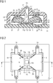
- a light source according to FIG. 1 is constructed on a circuit carrier 11, which is provided for protection with a housing structure 12.
- the housing structure 12 has the shape of a cap and is seated on the circuit carrier 11.
- Light-emitting diodes 13r, 13g and sensor elements 1a, 1b are mounted on the circuit carrier. Both the sensor elements 2a, 2b (as well as 1a, 1b, cf. FIG. 2 ) and the LEDs 13r, 13g (as well as 13y, cf. FIG. 2 ) are designed as SMD components and inexpensively mounted on the surface of the circuit substrate 11 by means of common SMD methods.
- the light emitting diodes 13r, 13g are also surrounded by a holding frame 16, which serves as a bearing surface for a light guide 17, which is also held in the housing structure 12.
- the side of the light-emitting diodes 13r, 13g two optical deflection elements 18 are arranged, which are held by adjusting devices 19 in the form of pins in holes 20 of the housing structure 12 and the circuit substrate 11. This allows at the same time a precise alignment of the deflecting elements 18 to the circuit carrier 11, the housing structure 12 to the deflection elements 18 and thus indirectly also an orientation of the light guide 17, which is held in the housing structure 12 fit.
- the radiating surfaces of the light-emitting diodes 13r, 13g point away from the mounting side of the circuit substrate 11.
- FIG. 1 are characteristic optical paths of the light emitted by the light emitting diode 13g shown.
- the radiation, which is detected by the light guide 17, forms the useful light 21. This is emitted at a diffuse radiating surface 22 as a light signal 23 to the environment.
- the light which is not led out of the housing structure 12 by the light-guiding element 17 is the residual light. Part of this residual light 23 is through the deflection 18 on the sensor surfaces of the sensor elements 2a, 2b (and 1a, 1b, see. FIG. 2 ).
- two beam paths are shown by way of example.
- the residual light is coupled through an entrance surface 24 into the respective deflection element and reflected by total reflection at a reflection surface 25 and / or at a curved reflection surface 26 and passed through an exit surface 27 on the sensor surface of the sensor elements 2a, 2b.
- a gap 28 which according to FIG. 1 is filled with air, but in a manner not shown may also be filled with an optical medium (potting). Since the deflection elements are constructed identically, the entry surface 24, the reflection surface 25, the curved reflection surface 26, the exit surface 27 can be found in the same way on both deflection elements.
- the curved reflection surface 26 is additionally coated with a mirror layer 29, so that the coupled-in residual light can be reliably deflected to the sensor elements 2b, 2a, even if the reflection angle would not allow total reflection without mirroring.
- the arrangement of the five used light emitting diodes can be the arrangement of the five used light emitting diodes recognize.
- a single light emitting diode 13y is provided for yellow light. This can produce yellow light in a sufficient light intensity, which is why a single light emitting diode 13y is sufficient. Therefore, this is provided in the center of the arrangement.
- red light two LEDs 13r and green light two LEDs 13g are provided.
- the light-emitting diodes 13r and 13g are each arranged diagonally from the yellow light-emitting diode 13y located in the center. Surrounding the light emitting diodes of the support frame 16 for the light guide 17, which as well as the housing structure 12 in FIG. 2 was omitted.
- the side of the light emitting diodes 13r, 13g, 13y, the deflecting elements 18 are arranged. These are in accordance with FIG. 2 above the mounted on the circuit substrate 11 sensor elements 1a, 1b, 2a, 2b. Therefore, the light exit surfaces 27 are according to FIG. 1 in FIG. 2 not recognizable. Also, the light entry surfaces 24 according to FIG. 1 , which are located in the oblique region of the deflecting elements 18, are in FIG. 2 not recognizable. However, it can be in FIG. 2 recognize that the width b of these entry surfaces is selected so that the outer LEDs 13g, 13r of the entrance surface only partially, in particular half of its width, are covered.
- each one of the two deflection elements are each very close to the entrance surface 24 each one of the two deflection elements.
- the single, lying in the center LED 13y is located farther from the entrance surfaces, but is exactly positioned in the middle of the width dimension b of the deflecting elements.
- the width b of the entrance surface is chosen such that the partial overlap of the entrance surface with the light emitting diodes 13g, 13r causes a portion of the residual light meet on side surfaces 30 of the deflecting element. These are coated with an opaque layer 31, so that this residual light can not be coupled into the respective deflecting element.
- FIGS. 3 and 4 another embodiment of the light source according to the invention is shown. It can be seen that the light-emitting diodes 13r, 13g, 13y are mounted in the same arrangement on the circuit carrier 11, as shown in FIG FIG. 2 is shown. Also, the holding frame 16 and the light guide 17 are used, a housing structure is not shown, but can as in FIG. 1 be formed represented.
- Auxiliary circuit carrier 32 are used, which are mounted on two opposite sides of the light emitting diodes 13r, 13g, 13y. These are perpendicular to the circuit board 11 and can be contacted for example via solder joints 33 with printed conductors not shown on the circuit substrate 11.
- the coupling of Nutzlicht 21 in the light guide 17 is analogous to that in FIG. 1 shown way. Rest light 23 falls directly without deflection on the sensor elements 1a, 1b, 2a, 2b. In this case, the residual light passes through the air lying between the light emitting diodes 13r, 13g, 13y and the sensor elements 1a, 1b, 2a, 2b. In FIG. 3 is shown how the remaining light 23 from the light emitting diode 13g strikes the sensor element 2b. In FIG. 3 the sensor element 1b, which lies exactly behind the illustrated sensor element 1a (see FIG. FIG. 4 ) and the sensor element 2a, which is located in FIG. 3 located directly behind the sensor element 2b.
- FIG. 4 It is shown how the sensor elements 1a, 1b are mounted on the auxiliary circuit carrier 32. These lie directly next to each other, with tracks 34 leading to metallized hole cutouts 35 in the auxiliary circuit carrier. These metallized hole cutouts then serve for contacting via the solder connections 33 with the circuit carrier 11.
- the sensor element 1a has a blue color shifted spectral sensitivity.
- the measurement signal for the green LED 13g in proportion to the amount of light turn out to be stronger than that of the closer red LED 13r. Overall, it comes therefore to a homogenization of the sensor signals at different colors.
- the sensor element 1b has a more uniform spectral photosensitivity. Since the arrangement of the light-emitting diodes 13r, 13g, 13y (as in FIG FIG. 2 ) is point-symmetrical, the sensor element 2b also has a spectral sensitivity shifted to blue, while the spectral sensitivity of the sensor element 2b is more uniform.
- the sensor elements 1a, 1b are used for monitoring the light source according to the FIGS. 1 to 4 . Due to the use of two sensor elements, it is possible to use the sensor element 1a, 1b for monitoring the light emitting diodes 13r, 13g, whose associated deflection element 18 or associated auxiliary circuit carrier 32 is closer to the respective light emitting diode. This results in a sufficiently high signal strength.
- the monitoring of the yellow light emitting diode 13y can be carried out in the same way by both sensor elements 1a, 1b.
- the sensor elements 1a, 1b supply the measurement signal in a manner not shown to an evaluation electronics in which, for example, an age-related change in the luminosity can be detected up to a failure of the LEDs. If necessary, the evaluation electronics can indicate the need for maintenance or repair of the light source.
- the detection of measurement signals by means of the sensor elements 2a, 2b is analogous to the manner described above. These sensor elements are arranged redundantly and are only used when the function of the monitoring by the sensor elements 1a, 1b is limited or failed. In this case, the same evaluation electronics as for controlling the sensor elements 1a, 1b can be used for monitoring, or redundant evaluation electronics are used.
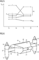
- FIG. 5 is shown how the too FIG. 2 described measure only a partial overlap of the entrance surfaces 24 leads with the light emitting diodes 13g, 13r to an equalization of the signal strength, which are generated by the different light colors red r, green g and yellow y.
- the generated measurement signals are applied in the form of the sensor voltage U sen . To represent the intensity profile, the respective measurement signals are connected to each other.
- the measure of only a partial overlap of the emission surface with the entry surface does not have any effect, since partial coverage is provided only for the red light r and the green light g.
- the intensity profile is recorded by dashed lines in the event that the light-emitting diodes 13g, 13r would have complete coverage with the entrance surface 24. Due to the partial overlap, however, a smaller proportion of the residual light is coupled into the deflecting element, which is why the intensity of the relevant measuring signals is lower. This results in a difference .DELTA.U with respect to the maximum generated sensor voltage U max (indicated for the red LED 13r).
- ⁇ U thus results from the difference of the generated sensor voltages U sen with partial coverage of the entrance surfaces 24 of the deflection element with the light emitting diode 13r and a dotted dashed sensor voltage for the light r, which would be measured at full coverage.
- FIG. 5 can be found in the FIG. 5 drawn ⁇ U the decisive contribution for equalization of the signal height U sen , since U max is generated by the red light r and U min by the yellow light y. As a result, the signal level provided by each color can be evened.
- the ratio between the maximum generated sensor voltage at the red light r and the minimum generated sensor voltage at the yellow light y U max / U min is approximately 1.7.
- FIG. 6 is the deflecting element 18 according to FIGS. 1 and 2 shown in three dimensions.
- This component can be advantageously produced as an injection molded part of an optical plastic.
- the entrance surface 25 and the side surfaces 30, which with the opaque layer 31 (see. FIG. 2 ) can be provided.
- the reflection surface 25 and the curved reflection surface 26 can be seen, wherein the latter can be provided with the mirror layer 29 (see FIG.
- the adjusting devices 19 are attached to side arms 36, which were made in one piece with the deflecting elements 18. Since the part was produced by injection molding, also the level of a parting line 37 of an injection mold, not shown, is indicated.
Landscapes
- Physics & Mathematics (AREA)
- General Physics & Mathematics (AREA)
- Engineering & Computer Science (AREA)
- General Engineering & Computer Science (AREA)
- Led Device Packages (AREA)
Abstract
Description
- Die Erfindung betrifft eine Lichtquelle für eine Signaleinrichtung, insbesondere von Verkehrswegen. Die Lichtquelle weist einen Schaltungsträger auf, auf dem mindestens eine Leuchtdiode mit einer vom Schaltungsträger weg gerichteten Abstrahlfläche für ein Signal bildendes Nutzlicht montiert ist. Das heißt, dass die Leuchtdiode Licht produziert, welches als Nutzlicht für das Signal gedacht ist. Allerdings kann auf Grund seines Abstrahlwinkels nicht das gesamte Licht der Leuchtdiode für das Signal genutzt werden, so dass auch Restlicht entsteht, welches nicht für das Signal genutzt wird. Das Nutzlicht kann beispielsweise durch die Eintrittsfläche eines Lichtleitelements aufgefangen werden, wobei das Lichtleitelement das Nutzlicht weiterleitet und als Signal der Signaleinrichtung abstrahlt. Dieses Signal kann beispielsweise zur Regulierung des Verkehrs von schienengebundenen oder straßengebundenen Fahrzeugen genutzt werden.
- Weiterhin weist die Lichtquelle ein optisches Sensorelement für die Leuchtdiode auf. Mit diesem Sensorelement kann die Leuchtdiode hinsichtlich ihrer Funktion oder ihrer Funktionsparameter, wie z. B. der abgestrahlten Lichtintensität überwacht werden. Zu diesem Zweck wird das durch das optische Sensorelement erzeugte Messsignal durch eine geeignete Auswertungseinheit verarbeitet.
- Außerdem betrifft die Erfindung auch eine Signaleinrichtung, insbesondere für Verkehrswege, mit einer Lichtquelle der oben angegebenen Art.
- Eine Lichtquelle und eine Signaleinrichtung der eingangs angegebenen Art ist beispielsweise in der
EP 2 163 455 A2 beschrieben. Eine solche Lichtquelle kann aus einer oder mehreren Leuchtdioden bestehen, wobei der Schaltungsträger mit den Leuchtdioden auch in ein konventionelles Signal eingebaut werden kann, welches für Glühlampen als Leuchtmittel vorbereitet ist. Hierbei muss die Lichtquelle mit der Leuchtdiode geeignete mechanische Schnittstellen aufweisen. - Zum Schutz der Leuchtdioden und der Lichtsensoren können diese in eine transparente Vergussmasse eingegossen sein. Diese Vergussmasse dient dann gleichzeitig dazu, das Restlicht von den Leuchtdioden zu den Sensorelementen zu leiten. Die entstehenden optischen Verluste führen dazu, dass das zur Verfügung stehende Nutzlicht verringert wird, so dass die Vergussmasse für eine Abschwächung des Signals verantwortlich ist.
- Die Aufgabe der Erfindung besteht darin, eine Lichtquelle bzw. eine Signaleinrichtung der eingangs angegebenen Art dahingehend zu verbessern, dass ein möglichst großer Anteil des durch die Leuchtdiode produzierten Lichts als Nutzlicht zur Erzeugung eines Lichtsignals zur Verfügung steht.
- Diese Aufgabe wird mit der eingangs angegebenen Lichtquelle erfindungsgemäß dadurch gelöst, dass die Abstrahlfläche als optische Schnittstelle zu Luft ausgebildet ist und das Sensorelement im Strahlengang von durch die Abstrahlfläche abgegebenen, für das Signal ungenutzten Restlicht angeordnet ist. Das Nutzlicht kann beispielsweise über eine Eintrittsfläche in ein Lichtleitelement eingekoppelt werden und durch dieses als Lichtsignal abgestrahlt werden. Die Leuchtdiode strahlt jedoch auch Licht ab, welches insbesondere aufgrund des Abstrahlwinkels nicht als Nutzlicht zur Verfügung steht. Dieses kann durch das Sensorelement detektiert werden und steht somit für eine Überwachung der Funktion der Lichtquelle zur Verfügung. Dabei wird die Intensität des mittels des Nutzlichts erzeugten Lichtsignals vorteilhaft nicht verringert, da das Restlicht funktionsbedingt immer zur Verfügung steht. Da die Abstrahlfläche der Leuchtdiode als optische Schnittstelle zu Luft ausgebildet ist, kann vorteilhaft eine optimal große Lichtmenge für das Nutzsignal zur Verfügung gestellt werden. Die mindestens eine Leuchtdiode und/oder das mindestens eine Sensorelement können beispielsweise als Nacktchips ausgeführt sein und direkt auf dem Schaltungsträger montiert werden. Gemäß einer vorteilhaften Ausgestaltung der Erfindung kann auch vorgesehen werden, dass die mindestens eine Leuchtdiode und/oder das mindestens eine Sensorelement als SMD-Bauelemente ausgeführt sind. Dabei handelt es sich um Bauelemente, die als sogenannte Surface Mounted Devices (SMD), also oberflächenmontierbare Bauelemente auf dem Schaltungsträger zum Einsatz kommen. Die SMD-Bauelemente weisen üblicherweise ein Gehäuse auf, in das der leuchtende oder lichtempfindliche Halbleiterbaustein eingebaut ist. Hierbei kann ein transparenter Verguss zum Einsatz kommen, wobei dieser bei der Leuchtdiode in SMD-Bauweise die Abstrahlfläche und somit die optische Schnittstelle zu Luft bildet.
- Gemäß einer besonderen Ausgestaltung der Erfindung ist vorgesehen, dass auf dem Schaltungsträger ein optisches Umlenkelement für Restlicht angeordnet ist, welches Restlicht auf das Sensorelement umlenkt. Das optische Umlenkelement weist vorzugsweise eine Eintrittsfläche und eine Austrittsfläche für das aufgefangene Restlicht auf. Hierbei handelt es sich nicht um das gesamte von der mindestens einen Leuchtdiode ausgesandte Restlicht. Vorteilhaft verbessert das optische Umlenkelement aber die Ausbeute hinsichtlich des für eine Überwachung zur Verfügung stehenden Restlichts, so dass vorteilhaft an mindestens einem Sensorelement ein stärkeres Messsignal erzeugt werden kann.
- Die Umlenkung des betreffenden Restlichts erfolgt vorzugsweise über mindestens eine Reflexionsfläche im Umlenkelement. Hierbei kann es sich um eine ebene Fläche handeln. Gemäß einer besonderen Ausgestaltung der Erfindung kann jedoch auch eine gekrümmte Reflexionsfläche zum Einsatz kommen, die das betreffende Restlicht auf das Sensorelement bündelt. Eine Bündelung hat den Vorteil, dass die Intensität des vom Sensorelement erzeugten Messsignals erhöht werden kann, da das Sensorelement nur eine räumlich begrenzte Detektionsfläche für das Restlicht zur Verfügung stellt.
- Die Reflexionsfläche kann abhängig von der Geometrie des Umlenkelements so ausgebildet sein, dass aufgrund des Unterschieds der optischen Dichte zwischen dem Material des Umlenkelements und der Umgebung (vorzugsweise Luft) eine Totalreflexion an der Reflexionsfläche stattfindet. Dies hängt im Wesentlichen davon ab, in welchem Winkel Restlicht auf die Reflexionsfläche trifft. Sollte eine Totalreflexion von Restlicht an der Reflexionsfläche nicht gewährleistet sein, so kann die Reflexionsfläche zusätzlich verspiegelt werden, indem eine Spiegelschicht auf die Reflexionsfläche des Umlenkelements aufgebracht wird.
- Gemäß einer weiteren Ausführung der Lichtquelle kann vorgesehen werden, dass mehrere Leuchtdioden mit unterschiedlichen abgestrahlten Lichtwellenlängen und unterschiedlichen Einbaupositionen auf dem Schaltungsträger montiert sind, wobei die Eintrittsfläche des Umlenkelements Restlicht der mehreren Leuchtdioden auffängt. Hierzu muss die Eintrittsfläche des Umlenkelements unter Berücksichtigung der Einbaupositionen der Leuchtdioden und der Einbauposition des Umlenkelements dimensioniert werden. Die so gebildete Lichtquelle kann vorteilhaft z. B. in Signaleinrichtungen für mehrfarbige Lichtsignale zum Einsatz kommen. Dies bedeutet, dass die Lichtsignale z. B. in rot, gelb und grün aus derselben Lichtaustrittsfläche der Signaleinrichtung kommen können, da die Lichtquelle in mehreren Farben leuchten kann.
- Wenn die Intensität des von einer Leuchtdiode ausgestrahlten Nutzlichts für das Lichtsignal nicht ausreicht, kann es auch nötig sein, dass mehrere Leuchtdioden einer Lichtwellenlänge (Farbe) in der Lichtquelle zum Einsatz kommen. Es ist von Vorteil, wenn Leuchtdioden einer bestimmten abgestrahlten Lichtwellenlänge in zentralsymmetrischer Anordnung auf dem Schaltungsträger montiert sind.
- Bei dem Einsatz mehrerer Leuchtdioden ist nach einer weiterführenden Ausgestaltung der Erfindung vorgesehen, dass Leuchtdioden, die bedingt durch ihren Abstand zur Eintrittsfläche und/oder durch ihre Lichtwellenlänge im Sensorelement ein stärkeres Signal erzeugen, am seitlichen Rand der Eintrittsfläche angeordnet sind und Leuchtdioden, die bedingt durch ihren Abstand zur Eintrittsfläche und/oder durch ihre Lichtwellenlänge im Sensorelement im Vergleich dazu ein schwächeres Signal erzeugen, im mittleren Bereich der Eintrittsfläche angeordnet sind. Hierbei wird die Lichtleistung der betreffenden Leuchtdioden im Nennbetrieb zugrundegelegt. Für die Stärke des durch das Sensorelement erzeugten Signals sind zwei Kriterien von Bedeutung. Der Abstand der Leuchtdioden zur Eintrittsfläche des Umlenkelements ist von Bedeutung, da der Anteil des durch das Umlenkelement aufgenommenen Restlichts umso größer wird, je näher diese an der Eintrittsfläche positioniert ist. Weiterhin kann die Stärke des Sensorsignals auch aufgrund der auf den Sensor treffenden Lichtwellenlänge bei gleicher Lichtintensität unterschiedlich hoch ausfallen.
- Diese Unterschiede führen dazu, dass die Messsignale bei Einsatz unterschiedlicher Leuchtdioden nicht die gleichen Signalhöhen der Messsignale liefern. Dies kann vorteilhaft jedoch dadurch kompensiert werden, dass die Leuchtdiode, die im Sensorelement das schwächere oder schwächste Signal erzeugt, in der Mitte der Eintrittsfläche angeordnet ist, so dass ein möglichst großer Anteil des Restlichts eingefangen wird. Die Leuchtdioden, die am Rand der Eintrittsfläche liegen, strahlen demgegenüber mit einem Teil des abgestrahlten Restlichts an der Eintrittsfläche vorbei, so dass dieses Restlicht nicht auf das Sensorelement geleitet werden kann. Durch Positionierung der Leuchtdioden vor der Eintrittsfläche kann somit die Signalhöhe an dem Sensorelement gezielt beeinflusst werden, so dass die Intensität der erzeugten Messsignale vergleichmäßigt wird. Dies hat den Vorteil, dass eine nachgeschaltete Auswertungseinheit in ihrem Dynamikbereich möglichst wenig eingeengt wird. Dies ermöglicht die Verwendung von kostengünstigen elektronischen Elementen der Auswertungseinheit, da diese nur einen kleineren Dynamikbereich abdecken müssen.
- Weiterhin kann besonders vorteilhaft vorgesehen werden, dass eine Seitenfläche des Umlenkelements, welche sich an den seitlichen Rand der Eintrittsfläche anschließt, nicht undurchlässig ausgeführt ist. Dies kann beispielsweise mittels einer lichtundurchlässigen Beschichtung erfolgen. Hierdurch wird gewährleistet, dass Restlicht, welches nicht durch die Eintrittsfläche des Umlenkelements gelangt ist, auch nicht durch den an die Eintrittsfläche angrenzenden Oberflächenbereich des Umlenkelements in dieses gelangt. Damit lässt sich vorteilhaft die Menge an Restlicht, die in das Umlenkelement eintreten soll, gezielt einstellen.
- Gemäß einer anderen Ausgestaltung der Erfindung ist vorgesehen, dass das Umlenkelement eine Austrittsfläche für das umgelenkte Licht aufweist und das Sensorelement direkt vor der Austrittsfläche angeordnet ist. Diese Anordnung kann vorzugsweise so ausgerichtet sein, dass auch die Sensorelemente auf dem Schaltungsträger montiert werden können. Die Sensorfläche des Sensorelements sowie die Austrittsfläche sind dann vorzugsweise parallel zur Oberfläche des Schaltungsträgers ausgerichtet.
- Eine Anordnung des Sensorelements direkt vor der Austrittsfläche hat den Vorteil, dass das aus dem Umlenkelement ausgekoppelte Restlicht zu einem möglichst großen Anteil auf die Sensorfläche des Sensorelements trifft. Zwischen dem Sensorelement und der Austrittsfläche kann ein Spalt vorgesehen sein, der durch das Restlicht überbrückt werden muss. Der Spalt kann als Toleranzausgleich bei der Montage dienen. Alternativ kann das Umlenkelement mit der Austrittsfläche auch direkt auf das Sensorelement aufgesetzt werden. Der Spalt kann auch durch ein optisch transparentes Medium wie eine Vergussmasse überbrückt werden.
- Vorteilhaft ist es auch, wenn das Umlenkelement an einer ersten Montagefläche für den Schaltungsträger und/oder an einer zweiten Montagefläche für eine Gehäusestruktur der Lichtquelle eine Justiervorrichtung aufweist. Diese kann beispielsweise durch einen Zapfen gebildet sein, welcher in geeignete Bohrungen oder Löcher im Schaltungsträger und/oder der Gehäusestruktur eingreift. Die Justiervorrichtungen erleichtern vorteilhaft die Montage und verbessern im montierten Zustand die vorstehend beschriebene Funktion des Umlenkelements, Restlicht verschiedener Leuchtdioden mit unterschiedlich großen Anteilen zum Sensorelement umzulenken.
- Gemäß einer anderen Ausgestaltung der Erfindung können zwei Umlenkelemente mit je einem Sensorelement (oder jeweils mehreren Sensorelementen, dazu im Folgenden noch mehr) vorgesehen sein, wobei die Umlenkelemente sich mit einander zugewandten Eintrittsflächen auf dem Schaltungsträger gegenüberliegen. Die mindestens eine Leuchtdiode ist dann zwischen den Eintrittsflächen auf dem Schaltungsträger angeordnet. Diese Anordnung ist dann besonders vorteilhaft, wenn mehrere Leuchtdioden an unterschiedlichen Einbaupositionen auf dem Schaltungsträger zum Einsatz kommen. Wenn diese aufgrund der Anordnungserfordernisse unterschiedliche Abstände zu jeweils dem einen Umlenkelement und dem anderen Umlenkelement aufweisen, kann durch den Einsatz zweier Umlenkelemente gewährleistet werden, dass immer genügend Restlicht der betreffenden Leuchtdiode entweder durch das eine Umlenkelement oder durch das andere Umlenkelement aufgenommen wird. Eine Überwachung der Gesamtheit der Leuchtdioden kann dadurch erfolgen, dass die durch die beiden betreffenden Sensorelemente aufgenommenen Messsignale voneinander unabhängig oder gemeinsam ausgewertet werden.
- Außerdem ist es vorteilhaft, wenn zwei unabhängig voneinander betreibbare Sensorelemente an der Austrittsfläche des Umlenkelements oder der Umlenkelemente vorgesehen sind. Diese Sensorelemente können vorteilhaft möglichst nah beieinander liegen. Die redundante Anordnung zweier Sensorelemente an einem Umlenkelement bewirkt vorteilhaft eine höhere Funktionszuverlässigkeit, da für den Fall, dass eines der Sensorelemente ausfällt, das Messsignal des anderen Sensorelements für eine Überwachung der Lichtquelle zum Einsatz kommen kann. Vorteilhaft wird standardmäßig das eine Sensorelement für eine Überwachung genutzt, während das zweite Sensorelement nur im Bedarfsfall zum Einsatz kommt, wenn das erste Sensorelement ausfällt. Selbstverständlich können auch zwei Umlenkelemente mit je zwei Sensorelementen zum Einsatz kommen.
- Gemäß einer alternativen Ausgestaltung der Erfindung kann vorgesehen werden, dass der Strahlengang des Restlichts zwischen der Abstrahlfläche der Leuchtdiode und dem Sensorelement ausschließlich durch Luft führt. Mit anderen Worten wird das Restlicht ohne Einsatz eines Umlenkelements direkt von der Abstrahlfläche der Leuchtdiode zu dem Sensorelement geführt. Hierbei entsteht vorteilhaft eine besonders kostengünstige Bauform, da auf die Montage von Umlenkelementen verzichtet werden kann.
- Gemäß einer Ausgestaltung dieser Erfindung kann vorgesehen werden, dass das Sensorelement auf einem Hilfsschaltungsträger angeordnet ist, welcher seitlich der Leuchtdiode senkrecht auf dem Schaltungsträger montiert ist. Das Sensorelement kann evtl. gemeinsam mit einer Auswertungsschaltung eine vormontierte Einheit bilden, die mit gut verfügbaren Verfahren der Elektronikmontage mit dem Schaltungsträger verbunden werden kann, welcher auch die Leuchtdioden trägt. Dabei entsteht ein rechter Winkel zwischen der Abstrahlfläche der Leuchtdiode und der Sensorfläche der Sensorelemente, wodurch vorteilhaft ein ausreichender Anteil des Restlichts durch das Sensorelement detektiert werden kann.
- Selbstverständlich ist es auch möglich, dass zwei Hilfsschaltungsträger mit je mindestens einem Sensorelement vorgesehen sind, wobei sich die Hilfsschaltungsträger mit einander zugewandten Sensorelementen auf dem Schaltungsträger gegenüberliegen. Die Leuchtdiode oder die Leuchtdioden sind dann zwischen den Hilfsschaltungsträgern montiert. Der Vorteil liegt darin, insbesondere bei mehreren Leuchtdioden immer ein Sensorelement zur Verfügung zu haben, welches Restlicht in einer genügenden Intensität empfangen kann.
- Auch bei dieser Alternative der Erfindung ist es möglich, dass zwei unabhängig voneinander betreibbare Sensorelemente auf den Hilfsschaltungsträgern vorgesehen sind, so dass für die Erstellung der Messsignale bei einem Ausfall des einen Sensorelements noch das andere Sensorelement zur Verfügung steht.
- Weiterhin kann vorteilhaft vorgesehen werden, dass mehrere Sensorelemente mit unterschiedlichen Lichtempfindlichkeiten für unterschiedliche Lichtwellenlängen auf dem Hilfsschaltungsträger angeordnet sind. So kann z. B. bei einem Einsatz von grünen Leuchtdioden eine Fotodiode mit einer in Richtung blau verschobenen spektralen Empfindlichkeit verwendet werden (angeboten beispielsweise durch die Firma Fist Sensor, Typ PS1.0-5b), wobei diese die entferntere Fotodiode in Bezug auf die grüne Leuchtdiode darstellt. Die nähere Fotodiode hat eine ausgeglichenere spektrale Empfindlichkeit (z. B. angeboten durch die Firma First Sensor, Typ PS1.0-5). Diese ist näher an der grünen Leuchtdiode angeordnet. Im Ergebnis ergibt sich dann ein ausgeglicheneres Verhältnis der gemessenen Spannungen an den Fotodioden.
- Die Aufgabe wird auch gelöst durch die eingangs angegebene Signaleinrichtung, bei der eine Lichtquelle nach einem der vorangehenden Ansprüche eingebaut ist. Die in der Signaleinrichtung eingebaute Lichtquelle weist die Vorteile auf, die oben bereits genau erläutert wurden.
- Weitere Einzelheiten der Erfindung werden nachfolgend anhand der Zeichnung beschrieben. Gleiche oder sich entsprechende Zeichnungselemente sind jeweils mit den gleichen Bezugszeichen versehen und werden nur insoweit mehrfach erläutert, wie sich Unterschiede zwischen den einzelnen Figuren ergeben.
- Bei den im Folgenden erläuterten Ausführungsbeispielen handelt es sich um bevorzugte Ausführungsformen der Erfindung. Bei den Ausführungsbeispielen stellen die beschriebenen Komponenten der Ausführungsformen jeweils einzelne, unabhängig voneinander zu betrachtende Merkmale der Erfindung dar, welche die Erfindung jeweils auch unabhängig voneinander weiterbilden und damit auch einzeln oder in einer anderen als der gezeigten Kombination als Bestandteil der Erfindung anzusehen sind. Des Weiteren sind die beschriebenen Ausführungsformen auch durch weitere der bereits beschriebenen Merkmale der Erfindung ergänzbar.
- Es zeigen:
- Figur 1
- ein Ausführungsbeispiel der erfindungsgemäßen Lichtquelle mit Umlenkelement schematisch im Schnitt,
- Figur 2
- eine Aufsicht auf das Ausführungsbeispiel gemäß Figur 1 ohne Gehäusestruktur, wobei in
Figur 2 der Schnitt I-I gemäßFigur 1 eingezeichnet ist (die Ausschnitte mit den Löchern 20 liegen in einer davon abweichenden Ebene), - Figur 3
- ein weiteres Ausführungsbeispiel der erfindungsgemäßen Lichtquelle mit Hilfsschaltungsträgern schematisch als Seitenansicht,
- Figur 4
- die Aufsicht auf einen Hilfsschaltungsträger gemäß
Figur 3 , - Figur 5
- Sensorspannungen von vier Sensorelementen für die Farben rot, grün und gelb schematisch,
- Figur 6
- ein Ausführungsbeispiel des umlenken Elementes, ausgeführt als Spritzgussteil, in dreidimensionaler Darstellung.
- Eine Lichtquelle gemäß
Figur 1 ist auf einem Schaltungsträger 11 aufgebaut, der zum Schutz mit einer Gehäusestruktur 12 versehen ist. Die Gehäusestruktur 12 hat die Form einer Kappe und setzt auf den Schaltungsträger 11 auf. - Auf dem Schaltungsträger sind Leuchtdioden 13r, 13g sowie Sensorelemente 1a, 1b montiert. Sowohl die Sensorelemente 2a, 2b (wie auch 1a, 1b, vgl.
Figur 2 ) und die Leuchtdioden 13r, 13g (wie auch 13y, vgl.Figur 2 ) sind als SMD-Bauelemente ausgeführt und mittels gängiger SMD-Verfahren kostengünstig auf der Oberfläche des Schaltungsträgers 11 montiert. Die Leuchtdioden 13r, 13g sind überdies von einem Halterahmen 16 umgeben, welcher als Auflagefläche für ein Lichtleitelement 17 dient, welches überdies in der Gehäusestruktur 12 gehalten ist. Weiterhin sind seitlich der Leuchtdioden 13r, 13g zwei optische Umlenkelemente 18 angeordnet, die über Justiervorrichtungen 19 in Form von Stiften in Löchern 20 der Gehäusestruktur 12 und des Schaltungsträgers 11 gehalten sind. Dies ermöglicht gleichzeitig eine passgenaue Ausrichtung der Umlenkelemente 18 zum Schaltungsträger 11, der Gehäusestruktur 12 zu den Umlenkelementen 18 und damit indirekt auch eine Ausrichtung des Lichtleitelements 17, welches passgenau in der Gehäusestruktur 12 gehalten ist. - Die Abstrahlflächen der Leuchtdioden 13r, 13g (und 13y, vgl.
Figur 2 ) weisen von der Montageseite des Schaltungsträgers 11 weg. InFigur 1 sind charakteristische Strahlengänge des durch die Leuchtdiode 13g abgestrahlten Lichts dargestellt. Die Strahlung, die vom Lichtleitelemente 17 erfasst wird, bildet das Nutzlicht 21. Dieses wird an einer diffusen Abstrahlfläche 22 als Lichtsignal 23 an die Umgebung abgegeben. Das Licht, welches nicht durch das Lichtleitelement 17 aus der Gehäusestruktur 12 ausgeleitet wird, ist das Restlicht. Ein Teils dieses Restlichts 23 wird durch die Umlenkelemente 18 auf die Sensorflächen der Sensorelemente 2a, 2b (sowie 1a, 1b, vgl.Figur 2 ) geleitet. Auch hier sind exemplarisch zwei Strahlengänge dargestellt. Das Restlicht wird durch eine Eintrittsfläche 24 in das jeweilige Umlenkelement eingekoppelt und durch Totalreflexion an einer Reflexionsfläche 25 und/oder an einer gekrümmten Reflexionsfläche 26 reflektiert und durch eine Austrittsfläche 27 auf die Sensorfläche der Sensorelemente 2a, 2b geleitet. - Zwischen der Austrittsfläche 27 und dem jeweiligen Sensorelement 2a, 2b befindet sich ein Spalt 28, der gemäß
Figur 1 mit Luft gefüllt ist, aber in nicht dargestellter Weise auch mit einem optischen Medium (Verguss) gefüllt sein kann. Da die Umlenkelemente identisch aufgebaut sind, finden sich die Eintrittsfläche 24, die Reflexionsfläche 25, die gekrümmte Reflexionsfläche 26, die Austrittsfläche 27 in gleicher Weise an beiden Umlenkelementen. Die gekrümmte Reflexionsfläche 26 ist zusätzlich mit einer Spiegelschicht 29 beschichtet, damit das eingekoppelte Restlicht zuverlässig auf die Sensorelemente 2b, 2a umgelenkt werden kann, auch wenn der Reflexionswinkel eine Totalreflexion ohne eine Verspiegelung nicht zulassen würde. - In der Aufsicht gemäß
Figur 2 lässt sich die Anordnung der fünf zum Einsatz kommenden Leuchtdioden erkennen. In der Mitte ist eine einzelne Leuchtdiode 13y für gelbes Licht vorgesehen. Diese kann gelbes Licht in einer genügenden Lichtintensität erzeugen, weswegen eine einzige Leuchtdiode 13y ausreicht. Daher ist diese im Zentrum der Anordnung vorgesehen. Für rotes Licht sind zwei Leuchtdioden 13r und für grünes Licht zwei Leuchtdioden 13g vorgesehen. Um eine zur optischen Achse des Lichtleitelements 17 zentralsymmetrische Anordnung zu gewährleisten, sind die Leuchtdioden 13r und 13g jeweils diagonal von der im Zentrum liegenden gelben Leuchtdiode 13y angeordnet. Umgeben werden die Leuchtdioden von dem Halterahmen 16 für das Lichtleitelement 17, welches ebenso wie die Gehäusestruktur 12 inFigur 2 weggelassen wurde. - Seitlich der Leuchtdioden 13r, 13g, 13y sind die Umlenkelemente 18 angeordnet. Diese befinden sich gemäß
Figur 2 oberhalb der auf dem Schaltungsträger 11 montierten Sensorelemente 1a, 1b, 2a, 2b. Daher sind auch die Lichtaustrittsflächen 27 gemäßFigur 1 inFigur 2 nicht zu erkennen. Auch die Lichteintrittsflächen 24 gemäßFigur 1 , die sich im schrägen Bereich der Umlenkelemente 18 befinden, sind inFigur 2 nicht zu erkennen. Allerdings lässt sich inFigur 2 erkennen, dass die Breite b dieser Eintrittsflächen so gewählt ist, dass die außenliegenden Leuchtdioden 13g, 13r von der Eintrittsfläche nur teilweise, insbesondere zur Hälfte ihrer Breite, überdeckt werden. Dafür liegen die äußeren Leuchtdioden 13g, 13r jeweils sehr nah an der Eintrittsfläche 24 je eines der beiden Umlenkelemente. Die einzelne, im Zentrum liegende Leuchtdiode 13y liegt entfernter von den Eintrittsflächen, ist dafür aber genau in der Mitte der Breitenausdehnung b der Umlenkelemente positioniert. - Wegen der größeren Entfernung der Leuchtiode 13y von der Eintrittsfläche 24 gelangt von dem Restlicht ein geringerer Betrag in das Umlenkelement, als wenn diese so nah an der Eintrittsfläche positioniert wäre, wie die Leuchtdioden 13g, 13r. Um die Menge des eingekoppelten Restlichts der Leuchtdioden 13g, 13r in das jeweils näher gelegene Umlenkelement zu verringern, ist die Breite b der Eintrittsfläche so gewählt, dass die nur teilweise Überdeckung der Eintrittsfläche mit den Leuchtdioden 13g, 13r dazu führt, dass ein Teil des Restlichts auf Seitenflächen 30 des Umlenkelements treffen. Diese sind mit einer lichtundurchlässigen Schicht 31 beschichtet, so dass dieses Restlicht nicht in das betreffende Umlenkelement eingekoppelt werden kann. Dies führt zu einer Annäherung der Lichtintensitäten des eingekoppelten Restlichts unabhängig davon, ob das Restlicht der Leuchtdiode 13g, das Restlicht der Leuchtdiode 13y oder das Restlicht der Leuchtdiode 13r in das jeweilige Umlenkelement eingekoppelt wird (hierzu im Folgenden noch mehr).
- Gemäß den
Figuren 3 und 4 ist ein anderes Ausführungsbeispiel der erfindungsgemäßen Lichtquelle dargestellt. Es ist zu erkennen, dass die Leuchtdioden 13r, 13g, 13y in derselben Anordnung auf dem Schaltungsträger 11 montiert sind, wie dies inFigur 2 dargestellt ist. Auch der Halterahmen 16 und das Lichtleitelement 17 kommen zum Einsatz, eine Gehäusestruktur ist nicht dargestellt, kann aber wie inFigur 1 dargestellt ausgebildet sein. - Anstelle von Lichtleitelementen kommen bei der Lichtquelle gemäß
Figur 3 Hilfsschaltungsträger 32 zum Einsatz, die auf zwei gegenüberliegenden Seiten der Leuchtdioden 13r, 13g, 13y montiert sind. Diese stehen senkrecht auf der Leiterplatte 11 und können beispielsweise über Lötverbindungen 33 mit nicht näher dargestellten Leiterbahnen auf den Schaltungsträger 11 kontaktiert sein. - Die Einkopplung von Nutzlicht 21 in das Lichtleitelement 17 erfolgt analog zu der in
Figur 1 dargestellten Weise. Restlicht 23 fällt direkt ohne Umlenkung auf die Sensorelemente 1a, 1b, 2a, 2b. Dabei durchquert das Restlicht die zwischen den Leuchtdioden 13r, 13g, 13y und den Sensorelementen 1a, 1b, 2a, 2b liegende Luft. InFigur 3 ist dargestellt, wie Restlicht 23 von der Leuchtdiode 13g auf das Sensorelement 2b trifft. InFigur 3 nicht zu erkennen ist das Sensorelement 1b, welches sich genau hinter dem dargestellten Sensorelement 1a befindet (vgl.Figur 4 ) und das Sensorelement 2a, welches sich inFigur 3 direkt hinter dem Sensorelement 2b befindet. - In
Figur 4 ist dargestellt, wie die Sensorelemente 1a, 1b auf den Hilfsschaltungsträger 32 montiert sind. Diese liegen direkt nebeneinander, wobei Leiterbahnen 34 zu metallisierten Lochausschnitten 35 in dem Hilfsschaltungsträger führen. Diese metallisierten Lochausschnitte dienen dann zur Kontaktierung über die Lotverbindungen 33 mit dem Schaltungsträger 11. - Das Sensorelemente 1a besitzt eine zur Farbe blau verschobene spektrale Empfindlichkeit. Hierdurch wird das Messsignal für die grüne Leuchtdiode 13g im Verhältnis zur Lichtmenge stärker ausfallen als das der näher gelegenen roten Leuchtdiode 13r. Insgesamt kommt es daher zu einer Vergleichmäßigung der Sensorsignale bei unterschiedlichen Farben. Das Sensorelemente 1b hat demgegenüber eine gleichmäßigere spektrale Lichtempfindlichkeit. Da die Anordnung der Leuchtdioden 13r, 13 g, 13y (wie in
Figur 2 ) punktsymmetrisch ist, weist auch das Sensorelement 2b eine nach blau verschobene spektrale Empfindlichkeit auf, während die spektrale Empfindlichkeit des Sensorelements 2b gleichmäßiger ist. - Für die Überwachung der Lichtquelle gemäß den
Figuren 1 bis 4 gilt, dass im Normalbetrieb jeweils die Sensorelemente 1a, 1b zum Einsatz kommen. Aufgrund der Verwendung zweier Sensorelemente ist es möglich, zur Überwachung der Leuchtdioden 13r, 13g jeweils das Sensorelement 1a, 1b zu nutzen, dessen zugeordnetes Umlenkelement 18 bzw. zugeordnete Hilfsschaltungsträger 32 näher an der betreffenden Leuchtdiode liegt. Hierbei entsteht eine genügend hohe Signalstärke. Die Überwachung der gelben Leuchtdiode 13y kann in gleicher Weise durch beide Sensorelemente 1a, 1b erfolgen. Zum Zwecke der Überwachung liefern die Sensorelemente 1a, 1b das Messsignal in nicht näher dargestellter Weise an eine Auswertungselektronik, in der beispielsweise eine alterungsbedingte Änderung der Leuchtkraft bis hin zu einem Ausfall der Leuchtdioden erfasst werden kann. Im Bedarfsfall kann die Auswertungselektronik den Bedarf einer Wartung oder Reparatur der Lichtquelle anzeigen. - Die Erfassung von Messsignalen mittels der Sensorselemente 2a, 2b erfolgt analog zu der oben beschriebenen Weise. Diese Sensorelemente sind redundant angeordnet und kommen nur zum Einsatz, wenn die Funktion der Überwachung durch die Sensorelemente 1a, 1b eingeschränkt oder ausgefallen ist. Dabei kann für eine Überwachung dieselbe Auswertungselektronik wie für die Ansteuerung der Sensorelemente 1a, 1b zum Einsatz kommen, oder es wird eine redundante Auswertungselektronik verwendet. In
Figur 5 ist dargestellt, wie die zuFigur 2 beschriebene Maßnahme einer nur teilweisen Überdeckung der Eintrittsflächen 24 mit den Leuchtdioden 13g, 13r zu einer Vergleichmäßigung der Signalstärke führt, die durch die unterschiedlichen Lichtfarben rot r, grün g und gelb y erzeugt werden. Für die vier Sensorelemente 1a, 1b, 2a, 2b sind die erzeugten Messsignale in Form der Sensorspannung Usen aufgetragen. Um das Intensitätsprofil darzustellen, sind die jeweiligen Messsignale miteinander verbunden. - Für das gelbe Licht y wirkt sich die Maßnahme einer nur teilweisen Überdeckung der Abstrahlfläche mit der Eintrittsfläche nicht aus, da eine teilweise Überdeckung nur für das rote Licht r und das grüne Licht g vorgesehen sind. Für diese beiden Farben ist jeweils gestrichelt das Intensitätsprofil aufgezeichnet für den Fall, dass die Leuchtdioden 13g, 13r eine vollständige Überdeckung mit der Eintrittsfläche 24 haben würden. Durch die nur teilweise Überdeckung wird jedoch ein geringerer Anteil des Restlichts in das Umlenkelement eingekoppelt, weswegen die Intensität der betreffenden Messsignale geringer ausfällt. Hierdurch ergibt sich ein Unterschied ΔU hinsichtlich der maximal erzeugten Sensorspannung Umax (eingezeichnet für die rote Leuchtdiode 13r). ΔU ergibt sich somit aus dem Unterschied der erzeugten Sensorspannungen Usen bei teilweiser Überdeckung der Eintrittsflächen 24 des Umlenkungselements mit der Leuchtdiode 13r und einer gestrichelt eingezeichneten Sensorspannung für das Licht r, welches bei vollständiger Überdeckung gemessen würde. Wie sich
Figur 5 entnehmen lässt, liefert das inFigur 5 eingezeichnete ΔU den ausschlaggebenden Beitrag für eine Vergleichmäßigung der Signalhöhe Usen, da Umax durch die rote Licht r erzeugt wird und Umin durch die gelbe Licht y. Infolgedessen lässt sich die durch die einzelnen Farben gelieferte Signalhöhe vergleichmäßigen. Im vorliegenden Fall der Verwendung von roten, grünen und gelben Leuchtdioden liegt das Verhältnis zwischen der maximal erzeugten Sensorspannung beim roten Licht r und der minimal erzeugten Sensorspannung beim gelben Licht y Umax/Umin bei ungefähr 1,7. - In
Figur 6 ist das Umlenkelement 18 gemäßFigur 1 und 2 dreidimensional dargestellt. Dieses Bauteil lässt sich vorteilhaft als Spritzgussteil aus einem optischen Kunststoff herstellen. Zu erkennen sind hier die Eintrittsfläche 25 und die Seitenflächen 30, die mit der lichtundurchlässigen Schicht 31 (vgl.Figur 2 ) versehen werden können. Außerdem ist die Reflexionsfläche 25 sowie die gekrümmte Reflexionsfläche 26 zu erkennen, wobei letztere mit der Spiegelschicht 29 (vgl. Figur 1) versehen werden kann. - Die Justiervorrichtungen 19 sind an Seitenarmen 36 befestigt, die einstückig mit dem Umlenkelemente 18 hergestellt wurden. Da das Teil durch Spritzgießen hergestellt wurde, ist außerdem die Ebene einer Trennfuge 37 einer nicht dargestellten Spritzgießform angedeutet.
Claims (15)
- Lichtquelle für eine Signaleinrichtung, insbesondere von Verkehrswegen, aufweisend• einen Schaltungsträger (11), auf dem mindestens eine Leuchtdiode (13r, 13g, 13y) mit einer vom Schaltungsträger (11) weg gerichteten Abstrahlfläche für ein Signal bildendes Nutzlicht montiert ist,• mindestens ein optisches Sensorelement (1a, 1b, 2a, 2b) für die Leuchtdiode (13r, 13g, 13y),dadurch gekennzeichnet,
dass die Abstrahlfläche als optische Schnittstelle zu Luft ausgebildet ist und das Sensorelement (1a, 1b, 2a, 2b) im Strahlengang von durch die Abstrahlfläche abgegebenen, für das Signal ungenutztem Restlicht angeordnet ist. - Lichtquelle nach Anspruch 1,
dadurch gekennzeichnet,
dass die Leuchtdiode (13r, 13g, 13y) und/oder das Sensorelement (1a, 1b, 2a, 2b) als SMD-Bauelemente ausgeführt sind. - Lichtquelle nach einem der voranstehenden Ansprüche,
dadurch gekennzeichnet,
dass auf dem Schaltungsträger (11) ein optisches Umlenkelement (18) für Restlicht angeordnet ist, welches Restlicht auf das Sensorelement (1a, 1b, 2a, 2b) umlenkt. - Lichtquelle nach Anspruch 3,
dadurch gekennzeichnet,
dass das optische Umlenkelement (18) über eine gekrümmte Reflexionsfläche (26) verfügt, die Restlicht auf das Sensorelement (1a, 1b, 2a, 2b) bündelt. - Lichtquelle nach einem der Ansprüche 3 oder 4,
dadurch gekennzeichnet,
dass mehrere Leuchtdioden (13r, 13g, 13y) mit unterschiedlichen abgestrahlten Lichtwellenlängen in unterschiedlichen Einbaupositionen auf dem Schaltungsträger (11) montiert sind, wobei eine Eintrittsfläche (24) des Umlenkelementes (18) Restlicht der mehreren Leuchtdioden (13r, 13g, 13y) auffängt. - Lichtquelle nach Anspruch 5,
dadurch gekennzeichnet,
dass Leuchtdioden (13r, 13g, 13y), mit denen bedingt durch ihren Abstand zur Eintrittsfläche (24) und/oder durch ihre Lichtwellenlänge im Sensorelement (1a, 1b, 2a, 2b) ein stärkeres Signal erzeugbar ist, am seitlichen Rand der Eintrittsfläche (24) angeordnet sind und Leuchtdioden (13r, 13g, 13y), mit denen bedingt durch ihren Abstand zur Eintrittsfläche (24) und/oder durch ihre Lichtwellenlänge im Sensorelement (1a, 1b, 2a, 2b) ein schwächeres Signal erzeugbar ist, im mittleren Bereich der Eintrittsfläche (24) angeordnet sind. - Lichtquelle nach Anspruch 6,
dadurch gekennzeichnet,
dass eine Seitenfläche (30) des Umlenkelementes (18), welche sich an den seitlichen Rand der Eintrittsfläche (24) anschließt, lichtundurchlässig ausgeführt ist. - Lichtquelle nach einem der Ansprüche 3 bis 7,
dadurch gekennzeichnet,
dass das Umlenkelement (18) eine Austrittsfläche (27) für das umgelenkte Licht aufweist und das Sensorelement (1a, 1b, 2a, 2b) direkt vor der Austrittsfläche (27) angeordnet ist. - Lichtquelle nach einem der Ansprüche 3 bis 8,
dadurch gekennzeichnet,
dass das Umlenkelement (18) an einer ersten Montagefläche für den Schaltungsträger und/oder an einer zweiten Montagefläche für eine Gehäusestruktur (12) der Lichtquelle eine Justiervorrichtung (19) aufweist. - Lichtquelle nach einem der Ansprüche 3 bis 9,
dadurch gekennzeichnet,
dass zwei Umlenkelemente (18) mit je einem Sensorelement (1a, 1b, 2a, 2b) vorgesehen sind, wobei die Umlenkelemente (18) sich mit einander zugewandten Eintrittsflächen (24) auf dem Schaltungsträger (11) gegenüberliegen. - Lichtquelle nach einem der Ansprüche 3 bis 10,
dadurch gekennzeichnet,
dass zwei unabhängig voneinander betreibbare Sensorelemente (1a, 1b, 2a, 2b) an der Austrittsfläche (27) des Umlenkelements (18) vorgesehen sind. - Lichtquelle nach einem der Ansprüche 1 oder 2,
dadurch gekennzeichnet,
dass der Strahlengang des Restlichtes zwischen der Abstrahlfläche der Leuchtdiode (13r, 13g, 13y) und dem Sensorelement (1a, 1b, 2a, 2b) ausschließlich durch Luft führt. - Lichtquelle nach Anspruch 12,
dadurch gekennzeichnet,
dass das Sensorelement (1a, 1b, 2a, 2b) auf einem Hilfsschaltungsträger (32) angeordnet ist, welcher seitlich der Leuchtdiode (13r, 13g, 13y) senkrecht auf dem Schaltungsträger (11) montiert ist. - Lichtquelle nach Anspruch 12 oder 13,
dadurch gekennzeichnet,
dass Sensorelemente (1a, 1b, 2a, 2b) mit unterschiedlichen Lichtempfindlichkeiten für unterschiedliche Lichtwellenlängen auf dem Hilfsschaltungsträger (32) angeordnet sind. - Signaleinrichtung, insbesondere für Verkehrswege
dadurch gekennzeichnet,
dass eine Lichtquelle nach einem der vorangehenden Ansprüche in die Signaleinrichtung eingebaut ist.
Applications Claiming Priority (1)
| Application Number | Priority Date | Filing Date | Title |
|---|---|---|---|
| DE102017220615.2A DE102017220615A1 (de) | 2017-11-17 | 2017-11-17 | Lichtquelle für eine Signaleinrichtung mit Sensorelement zur Überwachung und Signaleinrichtung mit einer solchen Lichtquelle |
Publications (2)
| Publication Number | Publication Date |
|---|---|
| EP3486563A1 true EP3486563A1 (de) | 2019-05-22 |
| EP3486563B1 EP3486563B1 (de) | 2020-07-22 |
Family
ID=63921524
Family Applications (1)
| Application Number | Title | Priority Date | Filing Date |
|---|---|---|---|
| EP18201160.1A Active EP3486563B1 (de) | 2017-11-17 | 2018-10-18 | Lichtquelle für eine signaleinrichtung mit sensorelement zur überwachung und signaleinrichtung mit einer solchen lichtquelle |
Country Status (2)
| Country | Link |
|---|---|
| EP (1) | EP3486563B1 (de) |
| DE (1) | DE102017220615A1 (de) |
Citations (6)
| Publication number | Priority date | Publication date | Assignee | Title |
|---|---|---|---|---|
| EP0935145A1 (de) * | 1998-02-04 | 1999-08-11 | IMS Industrial Micro System AG | Optische Signal- und Anzeigevorrichtung |
| WO2002023954A1 (en) * | 2000-09-15 | 2002-03-21 | Koninklijke Philips Electronics N.V. | Led luminaire |
| WO2011067311A1 (en) * | 2009-12-04 | 2011-06-09 | Osram Gesellschaft mit beschränkter Haftung | Led lighting module with co-molded light sensor |
| WO2011086027A1 (de) * | 2010-01-15 | 2011-07-21 | Siemens Aktiengesellschaft | Lichtsignal |
| DE102015218156A1 (de) * | 2014-09-22 | 2016-03-24 | Swarco Futurit Verkehrssignalsysteme Gmbh | Hochbündelnde, farbmischende Signal- oder Scheinwerferoptik |
| DE102014219687A1 (de) * | 2014-09-29 | 2016-03-31 | Siemens Aktiengesellschaft | Signalgeber für eine Lichtsignalanlage und Lichtsignalanlage |
Family Cites Families (2)
| Publication number | Priority date | Publication date | Assignee | Title |
|---|---|---|---|---|
| DE102008047664A1 (de) | 2008-09-15 | 2010-05-20 | Fraunhofer-Gesellschaft zur Förderung der angewandten Forschung e.V. | Lichtsignal |
| AT510824B1 (de) * | 2010-11-23 | 2016-05-15 | Swarco Futurit Verkehrssignalsysteme Ges M B H | Farbmischende sammeloptik |
-
2017
- 2017-11-17 DE DE102017220615.2A patent/DE102017220615A1/de not_active Withdrawn
-
2018
- 2018-10-18 EP EP18201160.1A patent/EP3486563B1/de active Active
Patent Citations (6)
| Publication number | Priority date | Publication date | Assignee | Title |
|---|---|---|---|---|
| EP0935145A1 (de) * | 1998-02-04 | 1999-08-11 | IMS Industrial Micro System AG | Optische Signal- und Anzeigevorrichtung |
| WO2002023954A1 (en) * | 2000-09-15 | 2002-03-21 | Koninklijke Philips Electronics N.V. | Led luminaire |
| WO2011067311A1 (en) * | 2009-12-04 | 2011-06-09 | Osram Gesellschaft mit beschränkter Haftung | Led lighting module with co-molded light sensor |
| WO2011086027A1 (de) * | 2010-01-15 | 2011-07-21 | Siemens Aktiengesellschaft | Lichtsignal |
| DE102015218156A1 (de) * | 2014-09-22 | 2016-03-24 | Swarco Futurit Verkehrssignalsysteme Gmbh | Hochbündelnde, farbmischende Signal- oder Scheinwerferoptik |
| DE102014219687A1 (de) * | 2014-09-29 | 2016-03-31 | Siemens Aktiengesellschaft | Signalgeber für eine Lichtsignalanlage und Lichtsignalanlage |
Also Published As
| Publication number | Publication date |
|---|---|
| EP3486563B1 (de) | 2020-07-22 |
| DE102017220615A1 (de) | 2019-05-23 |
Similar Documents
| Publication | Publication Date | Title |
|---|---|---|
| EP2459795B1 (de) | Lichtabgabeeinrichtung für eine trommel eines haushaltsgeräts | |
| DE19922361C2 (de) | LED-Modul für Anzeigeeinrichtungen | |
| EP3312501A1 (de) | Beleuchtungsvorrichtung für fahrzeuge | |
| DE102012210743A1 (de) | Leuchtvorrichtung mit lichtsensor | |
| EP1327558A2 (de) | Fahrzeugleuchte | |
| EP3196539A1 (de) | Leuchtvorrichtung mit mehreren halbleiterlichtquellen | |
| DE102014215221A1 (de) | Beleuchtungsvorrichtung mit von einer Lichtquelle beabstandetem Leuchtstoffkörper | |
| DE10022420A1 (de) | Beleuchtungseinrichtung, insbesondere Leuchte, für Kraftfahrzeuge | |
| WO2016096600A1 (de) | Leuchtvorrichtung | |
| DE102017119500A1 (de) | Beleuchtungseinrichtung | |
| DE112016000316B4 (de) | Optoelektronisches Bauelement | |
| DE19646042A1 (de) | Beleuchtungseinrichtung für Fahrzeuge | |
| DE102013110345B4 (de) | Beleuchtungsvorrichtung für Fahrzeuge, die mindestens zwei Lichtmodule mit sich kreuzenden Lichtwegen aufweist | |
| DE10143415A1 (de) | Leuchtenanordnung | |
| DE112014001825B4 (de) | Fahrzeugleuchte | |
| DE102018206709A1 (de) | Beleuchtungssystem und scheinwerfer | |
| DE102010043296B4 (de) | Lichtemittermodul mit Umlenkoptik | |
| EP3486563B1 (de) | Lichtquelle für eine signaleinrichtung mit sensorelement zur überwachung und signaleinrichtung mit einer solchen lichtquelle | |
| EP2955063A1 (de) | Kraftfahrzeugleuchte | |
| DE102012104148A1 (de) | Optoelektronisches Halbleiterbauelement mit einem optischen Diffusorelement und Verfahren zum Herstellen eines derartigen Halbleiterbauelements | |
| EP1574880B2 (de) | Sendeelement für Lichtschranken, Lichtgitter und dergleichen | |
| WO2020108986A1 (de) | Fahrzeugleuchte und fahrzeug damit | |
| DE102014219687A1 (de) | Signalgeber für eine Lichtsignalanlage und Lichtsignalanlage | |
| EP3416852B1 (de) | Lichtmodul | |
| WO2017174659A1 (de) | Lichtquelle für eine beieuchtungsvorrichtung sowie beleuchtungsvorrichtung mit einer derartigen lichtquelle |
Legal Events
| Date | Code | Title | Description |
|---|---|---|---|
| PUAI | Public reference made under article 153(3) epc to a published international application that has entered the european phase |
Free format text: ORIGINAL CODE: 0009012 |
|
| STAA | Information on the status of an ep patent application or granted ep patent |
Free format text: STATUS: THE APPLICATION HAS BEEN PUBLISHED |
|
| AK | Designated contracting states |
Kind code of ref document: A1 Designated state(s): AL AT BE BG CH CY CZ DE DK EE ES FI FR GB GR HR HU IE IS IT LI LT LU LV MC MK MT NL NO PL PT RO RS SE SI SK SM TR |
|
| AX | Request for extension of the european patent |
Extension state: BA ME |
|
| STAA | Information on the status of an ep patent application or granted ep patent |
Free format text: STATUS: REQUEST FOR EXAMINATION WAS MADE |
|
| 17P | Request for examination filed |
Effective date: 20191122 |
|
| RBV | Designated contracting states (corrected) |
Designated state(s): AL AT BE BG CH CY CZ DE DK EE ES FI FR GB GR HR HU IE IS IT LI LT LU LV MC MK MT NL NO PL PT RO RS SE SI SK SM TR |
|
| GRAP | Despatch of communication of intention to grant a patent |
Free format text: ORIGINAL CODE: EPIDOSNIGR1 |
|
| STAA | Information on the status of an ep patent application or granted ep patent |
Free format text: STATUS: GRANT OF PATENT IS INTENDED |
|
| RIC1 | Information provided on ipc code assigned before grant |
Ipc: G08G 1/095 20060101ALI20200214BHEP Ipc: F21V 23/04 20060101AFI20200214BHEP Ipc: F21Y 115/10 20160101ALN20200214BHEP |
|
| INTG | Intention to grant announced |
Effective date: 20200324 |
|
| GRAS | Grant fee paid |
Free format text: ORIGINAL CODE: EPIDOSNIGR3 |
|
| GRAA | (expected) grant |
Free format text: ORIGINAL CODE: 0009210 |
|
| STAA | Information on the status of an ep patent application or granted ep patent |
Free format text: STATUS: THE PATENT HAS BEEN GRANTED |
|
| AK | Designated contracting states |
Kind code of ref document: B1 Designated state(s): AL AT BE BG CH CY CZ DE DK EE ES FI FR GB GR HR HU IE IS IT LI LT LU LV MC MK MT NL NO PL PT RO RS SE SI SK SM TR |
|
| REG | Reference to a national code |
Ref country code: GB Ref legal event code: FG4D Free format text: NOT ENGLISH |
|
| REG | Reference to a national code |
Ref country code: CH Ref legal event code: EP |
|
| REG | Reference to a national code |
Ref country code: DE Ref legal event code: R096 Ref document number: 502018001940 Country of ref document: DE |
|
| REG | Reference to a national code |
Ref country code: AT Ref legal event code: REF Ref document number: 1293738 Country of ref document: AT Kind code of ref document: T Effective date: 20200815 |
|
| REG | Reference to a national code |
Ref country code: IE Ref legal event code: FG4D Free format text: LANGUAGE OF EP DOCUMENT: GERMAN |
|
| REG | Reference to a national code |
Ref country code: CH Ref legal event code: NV Representative=s name: SIEMENS SCHWEIZ AG, CH |
|
| REG | Reference to a national code |
Ref country code: LT Ref legal event code: MG4D |
|
| PG25 | Lapsed in a contracting state [announced via postgrant information from national office to epo] |
Ref country code: ES Free format text: LAPSE BECAUSE OF FAILURE TO SUBMIT A TRANSLATION OF THE DESCRIPTION OR TO PAY THE FEE WITHIN THE PRESCRIBED TIME-LIMIT Effective date: 20200722 Ref country code: LT Free format text: LAPSE BECAUSE OF FAILURE TO SUBMIT A TRANSLATION OF THE DESCRIPTION OR TO PAY THE FEE WITHIN THE PRESCRIBED TIME-LIMIT Effective date: 20200722 Ref country code: BG Free format text: LAPSE BECAUSE OF FAILURE TO SUBMIT A TRANSLATION OF THE DESCRIPTION OR TO PAY THE FEE WITHIN THE PRESCRIBED TIME-LIMIT Effective date: 20201022 Ref country code: PT Free format text: LAPSE BECAUSE OF FAILURE TO SUBMIT A TRANSLATION OF THE DESCRIPTION OR TO PAY THE FEE WITHIN THE PRESCRIBED TIME-LIMIT Effective date: 20201123 Ref country code: HR Free format text: LAPSE BECAUSE OF FAILURE TO SUBMIT A TRANSLATION OF THE DESCRIPTION OR TO PAY THE FEE WITHIN THE PRESCRIBED TIME-LIMIT Effective date: 20200722 Ref country code: SE Free format text: LAPSE BECAUSE OF FAILURE TO SUBMIT A TRANSLATION OF THE DESCRIPTION OR TO PAY THE FEE WITHIN THE PRESCRIBED TIME-LIMIT Effective date: 20200722 Ref country code: FI Free format text: LAPSE BECAUSE OF FAILURE TO SUBMIT A TRANSLATION OF THE DESCRIPTION OR TO PAY THE FEE WITHIN THE PRESCRIBED TIME-LIMIT Effective date: 20200722 Ref country code: GR Free format text: LAPSE BECAUSE OF FAILURE TO SUBMIT A TRANSLATION OF THE DESCRIPTION OR TO PAY THE FEE WITHIN THE PRESCRIBED TIME-LIMIT Effective date: 20201023 Ref country code: NO Free format text: LAPSE BECAUSE OF FAILURE TO SUBMIT A TRANSLATION OF THE DESCRIPTION OR TO PAY THE FEE WITHIN THE PRESCRIBED TIME-LIMIT Effective date: 20201022 |
|
| PG25 | Lapsed in a contracting state [announced via postgrant information from national office to epo] |
Ref country code: RS Free format text: LAPSE BECAUSE OF FAILURE TO SUBMIT A TRANSLATION OF THE DESCRIPTION OR TO PAY THE FEE WITHIN THE PRESCRIBED TIME-LIMIT Effective date: 20200722 Ref country code: LV Free format text: LAPSE BECAUSE OF FAILURE TO SUBMIT A TRANSLATION OF THE DESCRIPTION OR TO PAY THE FEE WITHIN THE PRESCRIBED TIME-LIMIT Effective date: 20200722 Ref country code: PL Free format text: LAPSE BECAUSE OF FAILURE TO SUBMIT A TRANSLATION OF THE DESCRIPTION OR TO PAY THE FEE WITHIN THE PRESCRIBED TIME-LIMIT Effective date: 20200722 Ref country code: IS Free format text: LAPSE BECAUSE OF FAILURE TO SUBMIT A TRANSLATION OF THE DESCRIPTION OR TO PAY THE FEE WITHIN THE PRESCRIBED TIME-LIMIT Effective date: 20201122 |
|
| PG25 | Lapsed in a contracting state [announced via postgrant information from national office to epo] |
Ref country code: NL Free format text: LAPSE BECAUSE OF FAILURE TO SUBMIT A TRANSLATION OF THE DESCRIPTION OR TO PAY THE FEE WITHIN THE PRESCRIBED TIME-LIMIT Effective date: 20200722 |
|
| REG | Reference to a national code |
Ref country code: DE Ref legal event code: R097 Ref document number: 502018001940 Country of ref document: DE |
|
| PG25 | Lapsed in a contracting state [announced via postgrant information from national office to epo] |
Ref country code: SM Free format text: LAPSE BECAUSE OF FAILURE TO SUBMIT A TRANSLATION OF THE DESCRIPTION OR TO PAY THE FEE WITHIN THE PRESCRIBED TIME-LIMIT Effective date: 20200722 Ref country code: IT Free format text: LAPSE BECAUSE OF FAILURE TO SUBMIT A TRANSLATION OF THE DESCRIPTION OR TO PAY THE FEE WITHIN THE PRESCRIBED TIME-LIMIT Effective date: 20200722 Ref country code: EE Free format text: LAPSE BECAUSE OF FAILURE TO SUBMIT A TRANSLATION OF THE DESCRIPTION OR TO PAY THE FEE WITHIN THE PRESCRIBED TIME-LIMIT Effective date: 20200722 Ref country code: RO Free format text: LAPSE BECAUSE OF FAILURE TO SUBMIT A TRANSLATION OF THE DESCRIPTION OR TO PAY THE FEE WITHIN THE PRESCRIBED TIME-LIMIT Effective date: 20200722 Ref country code: CZ Free format text: LAPSE BECAUSE OF FAILURE TO SUBMIT A TRANSLATION OF THE DESCRIPTION OR TO PAY THE FEE WITHIN THE PRESCRIBED TIME-LIMIT Effective date: 20200722 Ref country code: DK Free format text: LAPSE BECAUSE OF FAILURE TO SUBMIT A TRANSLATION OF THE DESCRIPTION OR TO PAY THE FEE WITHIN THE PRESCRIBED TIME-LIMIT Effective date: 20200722 |
|
| PLBE | No opposition filed within time limit |
Free format text: ORIGINAL CODE: 0009261 |
|
| STAA | Information on the status of an ep patent application or granted ep patent |
Free format text: STATUS: NO OPPOSITION FILED WITHIN TIME LIMIT |
|
| PG25 | Lapsed in a contracting state [announced via postgrant information from national office to epo] |
Ref country code: AL Free format text: LAPSE BECAUSE OF FAILURE TO SUBMIT A TRANSLATION OF THE DESCRIPTION OR TO PAY THE FEE WITHIN THE PRESCRIBED TIME-LIMIT Effective date: 20200722 |
|
| 26N | No opposition filed |
Effective date: 20210423 |
|
| PG25 | Lapsed in a contracting state [announced via postgrant information from national office to epo] |
Ref country code: LU Free format text: LAPSE BECAUSE OF NON-PAYMENT OF DUE FEES Effective date: 20201018 Ref country code: SK Free format text: LAPSE BECAUSE OF FAILURE TO SUBMIT A TRANSLATION OF THE DESCRIPTION OR TO PAY THE FEE WITHIN THE PRESCRIBED TIME-LIMIT Effective date: 20200722 Ref country code: MC Free format text: LAPSE BECAUSE OF FAILURE TO SUBMIT A TRANSLATION OF THE DESCRIPTION OR TO PAY THE FEE WITHIN THE PRESCRIBED TIME-LIMIT Effective date: 20200722 |
|
| REG | Reference to a national code |
Ref country code: BE Ref legal event code: MM Effective date: 20201031 |
|
| PG25 | Lapsed in a contracting state [announced via postgrant information from national office to epo] |
Ref country code: FR Free format text: LAPSE BECAUSE OF NON-PAYMENT OF DUE FEES Effective date: 20201031 |
|
| PG25 | Lapsed in a contracting state [announced via postgrant information from national office to epo] |
Ref country code: SI Free format text: LAPSE BECAUSE OF FAILURE TO SUBMIT A TRANSLATION OF THE DESCRIPTION OR TO PAY THE FEE WITHIN THE PRESCRIBED TIME-LIMIT Effective date: 20200722 Ref country code: BE Free format text: LAPSE BECAUSE OF NON-PAYMENT OF DUE FEES Effective date: 20201031 |
|
| REG | Reference to a national code |
Ref country code: NL Ref legal event code: MP Effective date: 20200722 |
|
| PG25 | Lapsed in a contracting state [announced via postgrant information from national office to epo] |
Ref country code: IE Free format text: LAPSE BECAUSE OF NON-PAYMENT OF DUE FEES Effective date: 20201018 |
|
| PG25 | Lapsed in a contracting state [announced via postgrant information from national office to epo] |
Ref country code: TR Free format text: LAPSE BECAUSE OF FAILURE TO SUBMIT A TRANSLATION OF THE DESCRIPTION OR TO PAY THE FEE WITHIN THE PRESCRIBED TIME-LIMIT Effective date: 20200722 Ref country code: MT Free format text: LAPSE BECAUSE OF FAILURE TO SUBMIT A TRANSLATION OF THE DESCRIPTION OR TO PAY THE FEE WITHIN THE PRESCRIBED TIME-LIMIT Effective date: 20200722 Ref country code: CY Free format text: LAPSE BECAUSE OF FAILURE TO SUBMIT A TRANSLATION OF THE DESCRIPTION OR TO PAY THE FEE WITHIN THE PRESCRIBED TIME-LIMIT Effective date: 20200722 |
|
| PG25 | Lapsed in a contracting state [announced via postgrant information from national office to epo] |
Ref country code: MK Free format text: LAPSE BECAUSE OF FAILURE TO SUBMIT A TRANSLATION OF THE DESCRIPTION OR TO PAY THE FEE WITHIN THE PRESCRIBED TIME-LIMIT Effective date: 20200722 |
|
| GBPC | Gb: european patent ceased through non-payment of renewal fee |
Effective date: 20221018 |
|
| PG25 | Lapsed in a contracting state [announced via postgrant information from national office to epo] |
Ref country code: GB Free format text: LAPSE BECAUSE OF NON-PAYMENT OF DUE FEES Effective date: 20221018 |
|
| PGFP | Annual fee paid to national office [announced via postgrant information from national office to epo] |
Ref country code: CH Payment date: 20250114 Year of fee payment: 7 |
|
| REG | Reference to a national code |
Ref country code: DE Ref legal event code: R081 Ref document number: 502018001940 Country of ref document: DE Owner name: SIEMENS MOBILITY GMBH, DE Free format text: FORMER OWNER: SIEMENS MOBILITY GMBH, 81739 MUENCHEN, DE |
|
| PGFP | Annual fee paid to national office [announced via postgrant information from national office to epo] |
Ref country code: AT Payment date: 20250905 Year of fee payment: 8 |
|
| REG | Reference to a national code |
Ref country code: CH Ref legal event code: U11 Free format text: ST27 STATUS EVENT CODE: U-0-0-U10-U11 (AS PROVIDED BY THE NATIONAL OFFICE) Effective date: 20260114 |
|
| PGFP | Annual fee paid to national office [announced via postgrant information from national office to epo] |
Ref country code: DE Payment date: 20251219 Year of fee payment: 8 |