EP3487058A1 - Commutation efficace pour circuit convertisseur - Google Patents
Commutation efficace pour circuit convertisseur Download PDFInfo
- Publication number
- EP3487058A1 EP3487058A1 EP18206400.6A EP18206400A EP3487058A1 EP 3487058 A1 EP3487058 A1 EP 3487058A1 EP 18206400 A EP18206400 A EP 18206400A EP 3487058 A1 EP3487058 A1 EP 3487058A1
- Authority
- EP
- European Patent Office
- Prior art keywords
- switch
- leg
- switches
- switching
- switch leg
- Prior art date
- Legal status (The legal status is an assumption and is not a legal conclusion. Google has not performed a legal analysis and makes no representation as to the accuracy of the status listed.)
- Granted
Links
Images




Classifications
-
- H—ELECTRICITY
- H02—GENERATION; CONVERSION OR DISTRIBUTION OF ELECTRIC POWER
- H02M—APPARATUS FOR CONVERSION BETWEEN AC AND AC, BETWEEN AC AND DC, OR BETWEEN DC AND DC, AND FOR USE WITH MAINS OR SIMILAR POWER SUPPLY SYSTEMS; CONVERSION OF DC OR AC INPUT POWER INTO SURGE OUTPUT POWER; CONTROL OR REGULATION THEREOF
- H02M7/00—Conversion of AC power input into DC power output; Conversion of DC power input into AC power output
- H02M7/42—Conversion of DC power input into AC power output without possibility of reversal
- H02M7/44—Conversion of DC power input into AC power output without possibility of reversal by static converters
- H02M7/48—Conversion of DC power input into AC power output without possibility of reversal by static converters using discharge tubes with control electrode or semiconductor devices with control electrode
- H02M7/53—Conversion of DC power input into AC power output without possibility of reversal by static converters using discharge tubes with control electrode or semiconductor devices with control electrode using devices of a triode or transistor type requiring continuous application of a control signal
- H02M7/537—Conversion of DC power input into AC power output without possibility of reversal by static converters using discharge tubes with control electrode or semiconductor devices with control electrode using devices of a triode or transistor type requiring continuous application of a control signal using semiconductor devices only, e.g. single switched pulse inverters
-
- H—ELECTRICITY
- H02—GENERATION; CONVERSION OR DISTRIBUTION OF ELECTRIC POWER
- H02M—APPARATUS FOR CONVERSION BETWEEN AC AND AC, BETWEEN AC AND DC, OR BETWEEN DC AND DC, AND FOR USE WITH MAINS OR SIMILAR POWER SUPPLY SYSTEMS; CONVERSION OF DC OR AC INPUT POWER INTO SURGE OUTPUT POWER; CONTROL OR REGULATION THEREOF
- H02M1/00—Details of apparatus for conversion
- H02M1/0048—Circuits or arrangements for reducing losses
-
- H—ELECTRICITY
- H02—GENERATION; CONVERSION OR DISTRIBUTION OF ELECTRIC POWER
- H02M—APPARATUS FOR CONVERSION BETWEEN AC AND AC, BETWEEN AC AND DC, OR BETWEEN DC AND DC, AND FOR USE WITH MAINS OR SIMILAR POWER SUPPLY SYSTEMS; CONVERSION OF DC OR AC INPUT POWER INTO SURGE OUTPUT POWER; CONTROL OR REGULATION THEREOF
- H02M1/00—Details of apparatus for conversion
- H02M1/08—Circuits specially adapted for the generation of control voltages for semiconductor devices incorporated in static converters
-
- H—ELECTRICITY
- H02—GENERATION; CONVERSION OR DISTRIBUTION OF ELECTRIC POWER
- H02M—APPARATUS FOR CONVERSION BETWEEN AC AND AC, BETWEEN AC AND DC, OR BETWEEN DC AND DC, AND FOR USE WITH MAINS OR SIMILAR POWER SUPPLY SYSTEMS; CONVERSION OF DC OR AC INPUT POWER INTO SURGE OUTPUT POWER; CONTROL OR REGULATION THEREOF
- H02M7/00—Conversion of AC power input into DC power output; Conversion of DC power input into AC power output
- H02M7/42—Conversion of DC power input into AC power output without possibility of reversal
- H02M7/44—Conversion of DC power input into AC power output without possibility of reversal by static converters
- H02M7/48—Conversion of DC power input into AC power output without possibility of reversal by static converters using discharge tubes with control electrode or semiconductor devices with control electrode
- H02M7/483—Converters with outputs that each can have more than two voltages levels
- H02M7/487—Neutral point clamped inverters
-
- H—ELECTRICITY
- H02—GENERATION; CONVERSION OR DISTRIBUTION OF ELECTRIC POWER
- H02M—APPARATUS FOR CONVERSION BETWEEN AC AND AC, BETWEEN AC AND DC, OR BETWEEN DC AND DC, AND FOR USE WITH MAINS OR SIMILAR POWER SUPPLY SYSTEMS; CONVERSION OF DC OR AC INPUT POWER INTO SURGE OUTPUT POWER; CONTROL OR REGULATION THEREOF
- H02M1/00—Details of apparatus for conversion
- H02M1/0048—Circuits or arrangements for reducing losses
- H02M1/0054—Transistor switching losses
-
- Y—GENERAL TAGGING OF NEW TECHNOLOGICAL DEVELOPMENTS; GENERAL TAGGING OF CROSS-SECTIONAL TECHNOLOGIES SPANNING OVER SEVERAL SECTIONS OF THE IPC; TECHNICAL SUBJECTS COVERED BY FORMER USPC CROSS-REFERENCE ART COLLECTIONS [XRACs] AND DIGESTS
- Y02—TECHNOLOGIES OR APPLICATIONS FOR MITIGATION OR ADAPTATION AGAINST CLIMATE CHANGE
- Y02B—CLIMATE CHANGE MITIGATION TECHNOLOGIES RELATED TO BUILDINGS, e.g. HOUSING, HOUSE APPLIANCES OR RELATED END-USER APPLICATIONS
- Y02B70/00—Technologies for an efficient end-user side electric power management and consumption
- Y02B70/10—Technologies improving the efficiency by using switched-mode power supplies [SMPS], i.e. efficient power electronics conversion e.g. power factor correction or reduction of losses in power supplies or efficient standby modes
-
- Y—GENERAL TAGGING OF NEW TECHNOLOGICAL DEVELOPMENTS; GENERAL TAGGING OF CROSS-SECTIONAL TECHNOLOGIES SPANNING OVER SEVERAL SECTIONS OF THE IPC; TECHNICAL SUBJECTS COVERED BY FORMER USPC CROSS-REFERENCE ART COLLECTIONS [XRACs] AND DIGESTS
- Y02—TECHNOLOGIES OR APPLICATIONS FOR MITIGATION OR ADAPTATION AGAINST CLIMATE CHANGE
- Y02E—REDUCTION OF GREENHOUSE GAS [GHG] EMISSIONS, RELATED TO ENERGY GENERATION, TRANSMISSION OR DISTRIBUTION
- Y02E10/00—Energy generation through renewable energy sources
- Y02E10/50—Photovoltaic [PV] energy
- Y02E10/56—Power conversion systems, e.g. maximum power point trackers
Definitions
- Power converters may be used for converting direct current (DC) voltage to a different DC voltage or an alternating current (AC) voltage.
- Converter construction may typically make use of power transistors and diodes.
- the power transistors and diodes may be operated as electronic switches.
- Certain converter designs may use "hard” switching, which may give rise to switching losses which, for high values of the switching frequency, may cause a reduction in energy conversion efficiency.
- Hard switching may be characterized by a total commutation voltage drop over the current-carrying switch at a current commutation time. In case of hard switching, the voltage may increase up to the value of the commutation voltage while the current continues flowing, before the voltage drops, that may cause high power loss peaks in the switch. It may therefore be desirable to develop converter topologies and switching methods that enable "soft" switching, which may reduce total switching losses.
- high-power converters may make use of a technique referred to as multi-level conversion.
- Multi-level converter design may reduce the occurrence of simultaneously high values of voltage and current, and hence high-power dissipation values, during the switching process. Additionally, multi-level converter topologies may provide multiple output voltage values, which may reduce the size of associated output filters. It may be desirable to develop converter topologies and efficient switching methodologies to improve the cost and/or efficiency of inverters.
- aspects disclosed herein may include an AC/DC converter (also known as an inverter) circuit and a method for converting direct current (DC) power at the inverter circuit input to an alternating current (AC) power at the inverter circuit output.
- the inverter circuit may include circuitry that may be configured to reduce switching and/or conduction losses of switches utilized in the inverter circuit to convert DC power to AC power, and the inverter circuit may provide auxiliary switches to reduce switching losses and to potentially increase efficiency of the inverter circuit.
- a switching leg may feature three 200V-rated MOSFET switches. During a switching cycle, the switching leg may alternate between the ON state (i.e., all three switches are ON) and the OFF state (where one or more of the three MOSFETs are OFF). If, for a first portion of a switching cycle, when in the OFF state the switching leg blocks no more than 200V, a single switch may be switched between the ON and OFF states, and two switches may be kept in the ON state throughout the first portion of the switching cycle. When the single switch is OFF, the switching leg dynamically blocks a voltage of up to 200V, and when the single switch is ON (along with the two switches kept in the ON state), the switching leg is conducting.
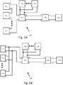
- the outputs on terminals A and B of the wiring configurations 111 may be connected in series to form a series connection of wiring configuration 111 outputs that may be connected to input terminals C and D of a link unit 107.
- Connected to terminals E and F of link unit 107 are multiple storage devices 106.
- Storage devices 106 may be batteries, flywheels and/ or super capacitors, for example.
- a feature of terminals E and F of link unit 107 may be that link unit 107 may be configurable in order to allow storage devices 106 to be charged from wiring configurations 111 and/or system power device 209 and/or discharged into load 104 via system power device 209.
- Input terminals P and Q of system power device 209 may be connected to terminals G and H of link unit 107.
- a feature of link units 107 may be to include a power device that may convert power bi-directionally.
- a first direction of power conversion by a power device (such as power device 103 described in descriptions that follow) may be when multiple storage devices 106 are sourced with converted power from the power devices.
- Storage devices 106 may receive converted power from the power devices when storage devices 106 are being charged, for example.
- a second direction of power conversion may be when power from storage devices 106 is converted by the power device to be supplied to loads 104 via system power device 209.
- Inverter 20a may have an input at terminals P and Q that may receive a DC voltage V dc from a source of DC power or from terminals G and H of switch unit 107.
- the source of DC power e.g., terminals G and H of switch unit 107
- V dc floating input voltage
- nodes N and Np may be may be considered to be connected to a neutral connection point that in electrical systems may be connected to earth or ground.
- connection to the neutral connection point in the description of inverters 20 that follow may provide a bipolar output with a peak AC voltage output at node A alternating between substantially plus V dc divided by two ( V dc /2) and substantially minus V dc divided by two (- V dc /2).
- the output at Node A may alternate for example between substantially plus V dc and substantially zero.
- the midpoint voltage may be substantially plus V dc divided by two ( V dc /2), and the output of inverter 20 may be considered to be unipolar.
- the drain ( d ) of switch SC3 may connect to terminal P and the source (s) of switch SC3 may connect to the drain ( d ) of switch SC4.
- the source of switch SC4 may connect to node A and to the drain ( d ) of switch SC5.
- the source of switch SC5 may connect to the drain ( d ) of switch SC6.
- the source of switch SC6 may connect to node Q.
- the three voltage levels may be substantially plus V dc divided by two ( V dc /2), substantially minus V dc divided by two (- V dc /2) and substantially zero (0) volts.
- the three voltage levels may correspond to three operating Switch States of inverter 20a. Further details of the three Switch States are detailed below when voltage V dc may be considered a bipolar input voltage to inverter 20a.
- Switches SC3, SC4, SC5 and SC6 may be 'OFF' and a first current flow from DC-link voltage ( V dc ) through the body diode of switch SC1, through switch SC2 ('PWM' applied) to node A or a second current flow in the opposite direction of the first current through the body diode of switch SC2 and through switch SC1.
- switches SC1 and SC2 may be MOSFETs, both switches SC1 and SC2 may be 'ON' and conduction via a body diode might not be utilized.
- Switch State 3 corresponding to negative V dc divided by two ( -V dc /2) at node A, a current flow may be through switches SC5 and SC6 (switches SC5 and SC6 may be 'ON') for a time period while switches SC1, SC2, SC3 and SC4 are 'OFF' for the time period.
- Current may flows through switches SC5 and through switch SC6 that are from node D and through node N (neutral) which may be connected to terminal Np (neutral).
- one of switch SC3 or switch SC4 may be 'ON' with a switching leg comprising switches SC3 and SC4 effectively 'OFF' by virtue of the other one of switches SC3 and SC4 being 'OFF'.
- switching legs 211 and 212 may be operated in 'PWM' mode (i.e., each of switching legs 211 and 212 alternate between conducting and dynamically blocking the voltage across capacitor C2 ), and switching leg 210 may be operated in 'OFF' mode, i.e., statically blocking the combined voltage across capacitors C1 and C2.
- 'PWM' mode i.e., each of switching legs 211 and 212 alternate between conducting and dynamically blocking the voltage across capacitor C2
- switching leg 210 may be operated in 'OFF' mode, i.e., statically blocking the combined voltage across capacitors C1 and C2.
- 'PWM' mode i.e., each of switching legs 211 and 212 alternate between conducting and dynamically blocking the voltage across capacitor C2
- switching leg 210 may be operated in 'OFF' mode, i.e., statically blocking the combined voltage across capacitors C1 and C2.
- SC6 may be either 'OFF' or 'ON' while maintaining the switching leg including switches SC5 and SC6 in the 'OFF' state.
- Switch State 1 where current from DC-link voltage ( V dc ) flows through switch SC3 ('PWM' applied) for a time period while switch SC4 stays substantially closed or 'ON' for the time period it may be possible that instead, current from_DC-link voltage ( V dc ) flows through switch SC4 ('PWM' applied) for a time period while switch SC3 stays substantially closed or 'ON' for the time period.
- the three Switch States may present the three discrete voltage levels ( +V dc /2,0v and - V dc /2) provided at node A.
- the result of the filtering of the AC voltage at node A applied to the input of filter 22 appears on the output of filter 22 on terminals J and K.
- filter 22 may reduce the amplitudes of the high frequency components of the voltage at node A to achieve an AC voltage on terminals J and K, which is more like a sine wave similar to that provided on a utility grid, for example.
- Voltage at node A is generated by operating switches SC1-SC6 to track waveform 24 in Fig. 2E .
- the control signals to control inverter 20a are shown as TR1, TR2, TR3, TR4 and TR5, which correspond respectively to the control signals applied to the gates of switches SC1/SC2, SC3, SC4, SC5 and SC6.
- the control signals applied to the gates of switches SC1/SC2, SC3, SC4, SC5 and SC6 are examples of pulse width modulation applied to the gates of switches SC1/SC2, SC3, SC4, SC5 and SC6 to track waveform 24.
- Control signal TR1 may be applied to leg 210.
- leg 210 is 'ON' by virtue of either of switch SC1 being on and the body diode of switch SC2 being conductive or by switch SC2 being on and the body diode of switch SC1 being conductive.
- Control signal TR2 may be applied to switch SC3, where when signal TR2 is 'high', switch SC3 is 'ON', and when TR2 is 'low', switch SC4 is 'OFF'.
- TR2 can be observed to switch between 'high' and 'low' at high frequency, indicating that switch SC3 is being operated in a 'PWM' switch state.
- switch TR2 can be observed to be only 'low', indicating that switch SC3 is being operated in an 'OFF' switch state.
- control signals TR3-TR5 may be applied to switches SC4-SC6, respectively.
- the output voltage VA varies at high frequency between 0V and V dc /2, current I1 is positive, and current I1 flows towards to node D.
- the commutation goes back and forth between leg 210 having switches SC3/SC4 and leg 212 having the bidirectional switch using switch SC2 and the body diode of switch SC1.
- current flows alternately through leg 210 and through leg 212.
- Legs 210 and 212 may each be operated in switch state 'PWM' - when leg 210 is ON, leg 212 is OFF (statically blocking the full voltage of at least V dc ), and vice-versa.
- both switches SC3 and SC4 When leg 210 is ON, both switches SC3 and SC4 are in switch state 'ON', and both switches SC1 and SC2 may be in switch state 'OFF'.
- a first switch e.g., SC4
- the second switch e.g., SC3
- switch state 'OFF' dynamically blocking a voltage of up to at least V dc /2.
- Switches SC3 and SC4 may each be rated to withstand a voltage of at least V dc /2, and switches SC3 and SC4 collectively may withstand a voltage of V dc applied between terminals P and Q.
- a first switch (e.g. SC5 ) of switches SC5 and SC6 may be in switch state 'ON', and the second switch (e.g. SC6 ) may be in switch state 'OFF'.
- Control signal TR5 may be observed to alternate at high frequency between 'high' and 'low', indicating the switch SC6 is being operating in switch state 'PWM'.
- both switches SC3 and SC4 may be OFF, and switches SC3 and SC4 may each be rated to withstand a voltage of at least V dc /2, such that when both switches SC3 and SC4 are OFF, leg 210 may withstand a voltage of at least V dc .
- current I1 is negative while voltage VA may alternate between 0V and V dc /2.
- Current I1 may commutate back and forth between leg 212 (via switch SC1 /body diode of switch SC2 ) and leg 210 (via the body diodes of switches SC3/SC4 ('OFF'), or by turning switch SC3 and/or SC4 ON.
- control signals TR3 and TR4 may be observed to be either continuously 'high' for a period of time (e.g. 220 or 230 ) or continuously 'low for a period of time, indicating that switches SC4 and SC5 are switched at low frequency (e.g., 50Hz or 60Hz) compared to switches SC3 and SC6 (controlled by control signals TR2 and TR5.
- the illustration of Fig. 2E is illustrative only - while control signals TR5 and TR2 are illustrated as switching about 20 times as fast as control signals TR3 and TR4. In practice, control signals TR5 and TR2 may switch 100, 1000 or even 20,000 times faster than control signals TR3 and TR4.
- two serially-connected switches may have reversed roles at different time periods.
- switch SC3 may be ON and switch SC4 may be operated in PWM mode (alternately conducting and dynamically blocking a voltage of at least V dc /2)
- switch SC4 may be ON and switch SC3 may be operated in PWM mode.
- PWM mode alternately conducting and dynamically blocking a voltage of at least V dc /2
- second time period 220 e.g., 20 milliseconds later, corresponding to a frequency of 50Hz
- switch SC4 may be ON and switch SC3 may be operated in PWM mode.
- heat caused by high-frequency switching may be generated at different locations on a circuit board, and overall heat dissipation may be improved.
- one of the switches in leg 210 may be an IGBT (and not a MOSFET, as illustrated) and one of the switches in leg 211 may be an IGBT (and not a MOSFET, as illustrated).
- An IGBT may provide lower conduction losses when compared to a MOSFET, but may suffer from inferior switching characteristics (e.g., higher switching losses).
- switches SC4 and SC5 using IGBTs switched at a low frequency (as shown by control signals TR3 and TR4 in Fig. 2E ), reduced conduction losses at legs 210 and 211 may be obtained.
- Switches SC3-SC6 in the manner illustrated in Fig. 2E may provide certain benefits. For example, switching losses (and heat generated) may be substantially reduced compared to an operation wherein all four switches are switched at a high frequency. As another potential benefit, each switch of switches SC3-SC6 may be rated to withstand a reduced voltage of only V dc /2.
- FIG. 2F illustrates an inverter 20b according to at least one aspect.
- Inverter 20b is similar to inverter 20a , with switching leg 218 replacing leg 210 of Fig. 2A and switching leg 219 replacing leg 211 of Fig. 2A .
- Switching leg 218 may comprise switch SC3 and switches SC40...SC4n.
- Switch SC3 may be operated similarly to as described with regard to Figs. 2A and 2E .
- Control signal TR2 of Fig. 2E may be applied to switch SC3.
- Switches SC40...SC4n may collectively replace switch SC4 of Fig. 2A .
- switch SC6 may be operated similarly to as described with regard to Figs. 2A and 2E .
- Control signal TR5 of Fig. 2E may be applied to switch SC5.
- Switches SC50...S54n may collectively replace switch SC5 of Fig. 2A .
- Switches SC3 and SC6 may be rated to withstand a voltage of at least V dc /2.
- Switches SC40...SC4n may each be rated to withstand a voltage of at least V dc /2n, where n is the number of switches in the group SC40...SC4n.
- Control signal Tr3 of Fig. 2E may be applied to switches SC40...SC4n.
- Switches SC50...SC5n may each be rated to withstand a voltage of at least V dc /2n, where n is the number of switches in the group SC50...SC5n, and control signal Tr4 of Fig. 2E may be applied to switches
- switches SC40...SC4n may be six switches (e.g., MOSFETs), each rated to withstand about 150V and having a conductance resistance ( R ds , on ) of about 3 m ⁇ , resulting in a total conductance resistance of about 20 m ⁇ (that may substantially reduce conductance losses across switches SC40...SC4n ).
- switches SC40...SC4n may be six switches (e.g., MOSFETs), each rated to withstand about 150V and having a conductance resistance ( R ds , on ) of about 3 m ⁇ , resulting in a total conductance resistance of about 20 m ⁇ (that may substantially reduce conductance losses across switches SC40...SC4n ).
- switches SC40...SC4n may be switched when switch SC3 is OFF and/or when leg 212 is ON, reducing the risk of an overvoltage across switches SC40...SC4n.
- switches SC50...SC5n may be switched when switch SC6 is OFF and/or when leg 212 is ON, reducing the risk of an overvoltage across switches
- switches SC40...SC4n may be ninety switches, each rated to withstand 10V, and collectively rated to withstand 900V. Switches SC40...SC4n might not be identical; any combination of voltage ratings summing to the desired total voltage rating may be used, which may provide great flexibility in design and potential cost reduction.
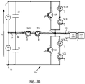
- FIG. 3A , 3B and 3C show an inverter 20c , according to at least one aspect.
- Inverter 20c is the same as inverter 20a except with respect to the connection of voltage V dc across terminals P and Q and use of main switches SC7 and SC8 with auxiliary switches SC3, SC4 and SC5, SC6.
- the connection of voltage V dc is a series connection of DC voltage sources V dc1 and V dc2 , where the connection between voltage sources V dc1 and V dc2 is connected to node N by link 30 .
- link 30 may be removed and V dc applied to terminals P and Q according to the description above with respect to Fig. 2A .
- connection between voltage sources V dc1 and V dc2 connected to node N may be when voltage sources V dc1 and V dc2 are provided from a series connection of photovoltaic panels that provide respective voltages V dc1 and V dc2 .
- Switches SC3-SC6 may be MOSFETs, as illustrated, and switches SC7 and SC8 may be different types of switches such as an IGBT, SiC or GaN switch.
- Figs. 3A , 3B and 3C correspond to the three Switch States of operation of inverter 20c to provide a three-level output at node A corresponding to V dc /2 , 0v and - V dc /2.
- Inverter 20c may be used as system power device 209 when system power device 209 may be or include an inverter.
- the role of switches SC3, SC4 and switches SC5, SC6 may be in an auxiliary role and may be respectively used to mitigate conduction losses of main switches SC7 and SC8.
- switches SC3, SC4 and switches SC5, SC6 in the description that follows are referred to as auxiliary switches.
- main switches SC7 and SC8 may be implemented as IGBTs
- a possible drawback to IGBTs may be their slower switching speed when compared with the switching speeds of MOSFETs for example.
- Mitigation of switching losses of main switches SC7 and SC8 may be such that on their own, main switches SC7 and SC8 are rated to block the full DC-link voltage Vdc, and may commutate at half the DC link voltage ( ⁇ V dc /2) when operated in 'PWM' mode.
- the use of auxiliary switches SC3, SC4, SC5, and SC6 may be utilized to compensate for possible conduction losses of main switches SC7 and SC8 as well as to compensate for possible increased switching losses of main switches SC7 and SC8 due to increased demand for higher DC link voltages ( V dc ).
- Main switch SC7 may be switched substantially in tandem with one of switches SC3 and SC4. For example, where SC3 is PWM-switched for time period 220 of Fig. 2E , main switch SC7 may be switched substantially at the same time as switch SC4. As will be discussed in greater detail below (see Fig. 4 ), a slight delay may be inserted when switching SC3 and SC7 in tandem, to provide zero-voltage switching conditions for switch SC7. Such a slight delay may correspond to a value between 1 ⁇ sec and 10 ⁇ sec in some aspects.
- Figs. 3A , 3B , 3C include marked areas in grey lines to indicate the commutation paths.
- the commutation paths may include an outer commutation path through leg 215 having main switch SC7 and auxiliary switches SC3/SC4, and an inner commutation path through leg 212 having a bidirectional switch composed of switches SC1 and SC2.
- the commutation paths may further include an outer commutation path through leg 216 having main switch SC8 and auxiliary switches SC5/SC6.
- the bidirectional switch allows the flow of current in two directions opposite to each other according to modes described in further detail below.
- the bidirectional nature of the bidirectional switch may be by the use of either SC2 and the body diode of switch SC1 or switch SC1 and the body diode of switch SC2 in order to enable the flow of current in two directions opposite to each other.
- control signals to control inverter 20c are shown as TR1, TR2, TR3, TR4 and TR5 that correspond respectively to the control signals applied to the gates of switches SC1/SC2, SC7/SC3, SC4, SC5 and SC6/SC8.
- inverter 20c may be controlled to achieve: desired voltage and current amplitudes, frequency, phase balancing, frequency-based power reduction, reactive power control, inverter reconnection conditions, levels of total harmonic distortion, power factor and output power control required by the utility grid and/or load.
- frequency modulation may be used or a control signal that includes a variable pulse width and frequency.
- the commutation paths may include a first outer commutation path through leg 215 having of main switch SC7 /auxiliary switches SC3/SC4 and an inner commutation path through leg 212 having a bidirectional switch composed of switches SC1 and SC2.
- the commutation paths may further include a second outer commutation path through leg 216 having main switch SC8 /auxiliary switches SC5/SC6 and through leg 212 having the bidirectional switch.
- switches SC3, SC4, SC5 and SC6 are used as main switches in inverter 20a.
- switching on of one of the switches is by application of PWM to the one switch for a time period whilst the other switch (e.g., switch SC4) remains 'ON' during the time period.
- the two switches are connected in series and operated in Switch State 1 such that switch SC4 is 'ON' before switch SC3 is on and switch SC3 goes 'OFF' before switch SC4 is 'OFF', the voltage across switch SC3 ('PWM' applied) is halved so switching losses are reduced and a possible problem of trying to control both switches SC3 and SC4 both being on may also be eliminated.
- the benefits of lower switching losses and simplified control of the possible problem of trying to control both switches SC3 and SC4 both being 'ON' may then further be added to the additional features of inverter 20c .
- Auxiliary switches SC3, SC4 and SC5, SC6 may be respectively connected in parallel to the main switches SC7 and SC8, which may help to move the switching losses away from main switches SC7 and SC8.
- the switching losses may move to the higher side of auxiliary switches SC3, SC5 while a substantial majority of current may still flow through main switches SC7 and SC8.
- two auxiliary switches may be connected in a series connection and the series connection connected across the main switch. Switching of the main switch may be by application of PWM to the main switch and one of the auxiliary switches for a time period with the other auxiliary switch remaining 'ON' during the time period.
- three auxiliary switches may be wired in series where switching of the main switch is by application of PWM to the main switch and one of the auxiliary switches for a time period with the other two auxiliary switches remaining 'ON' during the time period.
- Power converter 20d may feature a first switching leg 240 including hybrid switching circuit 241 connected in series to serial switching circuit 242.
- Hybrid switching circuit 241 may be arranged in a manner the same as or similar to switches SC3, SC4 and SC7 of Fig. 3A
- serial switching circuit 242 may include a series connection of switches (e.g., MOSFETs), similar to or the same as switches SC40...SC4n of Fig. 2F .
- Power converter 20d may further feature a second switching leg 250 including hybrid switching circuit 251 connected in series to serial switching circuit 252.
- Hybrid switching circuit 251 may be arranged in a manner the same as or similar to switches SC5, SC6 and SC8 of Fig. 3A
- serial switching circuit 252 may include a series connection of switches (e.g., MOSFETs).
- First switching leg 240 may alternate between an OFF mode of operation (e.g., where the switching leg 240 statically blocks the full input DC voltage for about half of a low-frequency time period, e.g., for about 10ms of a 20ms time period corresponding to a 50Hz frequency) and a PWM mode of operation (where the switching leg alternates, at high frequency, between (i) dynamically blocking half of the input DC voltage and (ii) conducting).
- OFF mode of operation all of the switches in switching leg 240 may be OFF.
- serial switching circuit 242 When in the PWM mode of operation, serial switching circuit 242 may be ON, and hybrid switching circuit 241 may alternate (at high frequency) between ON and OFF (dynamically blocking about half of the input DC voltage).
- hybrid switching circuit 241 may utilize a first switch (e.g., an IGBT) as a main switch, and one or more additional switches (e.g. MOSFETs) as auxiliary switching for reducing conduction losses.
- a first switch e.g., an IGBT
- additional switches e.g. MOSFETs
- Second switching leg 250 may be constructed and operated in a similar but complementary manner to first switching leg 240.
- Timing diagram 400 shows gate voltage signals that may be applied to switches SC3, SC4 and SC7 of Fig. 3A .
- Timing diagram 400 shows an auxiliary switch gate signal 401 and a main switch gate signal 402.
- the main switch may be, for example, switch SC7 of Fig. 3A
- the auxiliary switch may be, for example, switch SC3 of Fig. 3A (where switch SC4 may be switched at a low frequency) or switch SC4 of Fig. 3A (where switch SC3 may be switched at a low frequency).
- the main and auxiliary switches may be operated as follows:
- a benefit of wiring two or three auxiliary switches in a series connection across a main switch and/or mains switches connected and operated in series compared to a single main switch and/or single auxiliary switch may be that operating (i.e., blocking) voltage demands for the auxiliary switches may be reduced respectively by a half or a third by virtue of the series connection. Reduced voltages may reduce conduction losses of the switches. Reduction in operating voltage may reduce manufacturing cost of inverters due to overall cost of implementing series connections of main switches and/or auxiliary switches for Switch States 1, 2 and 3 compared to one main switch and/or one auxiliary switch for Switch States 1, 2 and 3, for example.
- switches may be applied to similar three phase inverter circuit implementations also.
- the same use of switches may be applied to other neutral point clamped inverter topologies for both three phase and single phase inverters.
- the same use of switches may also be similarly applied to multi-level inverters of various types.
Landscapes
- Engineering & Computer Science (AREA)
- Power Engineering (AREA)
- Inverter Devices (AREA)
- Dc-Dc Converters (AREA)
Priority Applications (1)
| Application Number | Priority Date | Filing Date | Title |
|---|---|---|---|
| EP23189078.1A EP4258532A3 (fr) | 2017-11-20 | 2018-11-15 | Commutation efficace pour circuit convertisseur |
Applications Claiming Priority (1)
| Application Number | Priority Date | Filing Date | Title |
|---|---|---|---|
| US201762588474P | 2017-11-20 | 2017-11-20 |
Related Child Applications (1)
| Application Number | Title | Priority Date | Filing Date |
|---|---|---|---|
| EP23189078.1A Division EP4258532A3 (fr) | 2017-11-20 | 2018-11-15 | Commutation efficace pour circuit convertisseur |
Publications (2)
| Publication Number | Publication Date |
|---|---|
| EP3487058A1 true EP3487058A1 (fr) | 2019-05-22 |
| EP3487058B1 EP3487058B1 (fr) | 2023-08-30 |
Family
ID=64331719
Family Applications (2)
| Application Number | Title | Priority Date | Filing Date |
|---|---|---|---|
| EP23189078.1A Pending EP4258532A3 (fr) | 2017-11-20 | 2018-11-15 | Commutation efficace pour circuit convertisseur |
| EP18206400.6A Active EP3487058B1 (fr) | 2017-11-20 | 2018-11-15 | Commutation efficace pour circuit convertisseur |
Family Applications Before (1)
| Application Number | Title | Priority Date | Filing Date |
|---|---|---|---|
| EP23189078.1A Pending EP4258532A3 (fr) | 2017-11-20 | 2018-11-15 | Commutation efficace pour circuit convertisseur |
Country Status (3)
| Country | Link |
|---|---|
| US (7) | US10536094B2 (fr) |
| EP (2) | EP4258532A3 (fr) |
| CN (1) | CN109861572B (fr) |
Cited By (2)
| Publication number | Priority date | Publication date | Assignee | Title |
|---|---|---|---|---|
| AT524166A1 (de) * | 2020-09-09 | 2022-03-15 | Ait Austrian Inst Tech Gmbh | Umrichter umfassend einen Zwischenkreis |
| WO2024012806A1 (fr) * | 2022-07-15 | 2024-01-18 | Gottfried Wilhelm Leibniz Universität Hannover | Procédé de fonctionnement d'un onduleur multiniveau hybride, onduleur multiniveau hybride et programme informatique |
Families Citing this family (16)
| Publication number | Priority date | Publication date | Assignee | Title |
|---|---|---|---|---|
| US10608624B2 (en) | 2017-05-25 | 2020-03-31 | Solaredge Technologies Ltd. | Efficient switching circuit |
| EP3676946B1 (fr) * | 2017-09-25 | 2021-12-29 | Huawei Digital Power Technologies Co., Ltd. | Onduleurs multiniveaux hybrides |
| US10536094B2 (en) | 2017-11-20 | 2020-01-14 | Solaredge Technologies Ltd. | Efficient switching for converter circuit |
| EP3675345A1 (fr) * | 2018-12-31 | 2020-07-01 | Solaredge Technologies Ltd. | Convertisseur de puissance à condensateurs équilibrées |
| US10517156B1 (en) * | 2019-01-25 | 2019-12-24 | Lumileds Holding B.V. | Hybrid driving scheme for RGB color tuning |
| CN110649831B (zh) * | 2019-05-10 | 2021-04-13 | 阳光电源股份有限公司 | 多电平逆变电路的关机封波控制方法及其应用装置 |
| US10652962B1 (en) | 2019-06-27 | 2020-05-12 | Lumileds Llc | Dim-to-warm LED circuit |
| EP3890179A1 (fr) * | 2020-04-02 | 2021-10-06 | Siemens Aktiengesellschaft | Convertisseur de puissance |
| CN111509992B (zh) * | 2020-04-30 | 2021-09-07 | 华为技术有限公司 | 交流电源电路、其控制方法及交流电源 |
| CN112583267B (zh) * | 2020-12-15 | 2022-06-07 | 山特电子(深圳)有限公司 | 双向dc-dc变换器及包括其的不间断电源 |
| CN113114061B (zh) * | 2021-03-26 | 2022-06-24 | 台达电子企业管理(上海)有限公司 | 变换器及抑制变换器的环流干扰的方法 |
| EP4315584A4 (fr) * | 2021-04-21 | 2024-05-22 | Huawei Digital Power Technologies Co., Ltd. | Convertisseur de puissance |
| US20240396423A1 (en) * | 2023-05-25 | 2024-11-28 | Advanced Energy Industries, Inc. | Phase shift scheme to optimize thermal efficiency for full-bridge converter |
| US20250226763A1 (en) * | 2024-01-10 | 2025-07-10 | Atieva, Inc. | Three-level inverter power module with multiple operation modes |
| TWI883927B (zh) * | 2024-01-24 | 2025-05-11 | 立錡科技股份有限公司 | 單電感雙極輸出電源轉換電路和相關控制方法 |
| US12565111B1 (en) | 2025-03-05 | 2026-03-03 | dcbel Inc. | Bidirectional split-phase power converter for electric vehicle charging |
Citations (6)
| Publication number | Priority date | Publication date | Assignee | Title |
|---|---|---|---|---|
| US20110193412A1 (en) * | 2010-02-05 | 2011-08-11 | Mge Ups | Converter device and uninterruptible power supply equipped with such a device |
| EP2413489A1 (fr) * | 2010-07-30 | 2012-02-01 | Vinotech Holdings S.à.r.l. | Convertisseur courant continu courant alternatif à demi-pont hautement efficace |
| WO2014082221A1 (fr) * | 2012-11-28 | 2014-06-05 | Eaton Corporation | Appareil convertisseur à plusieurs niveaux à dérivation de courant améliorant l'efficacité |
| EP2871765A1 (fr) * | 2013-11-08 | 2015-05-13 | Vincotech GmbH | Convertisseur NPC destiné à être utilisé dans un module de puissance et ledit module incorporant celui-ci |
| EP2953258A2 (fr) * | 2014-06-06 | 2015-12-09 | Delta Electronics (Shanghai) Co., Ltd. | Dispositif inverseur tnpc et son procede de detection de court-circuit |
| US20170302153A1 (en) * | 2016-04-19 | 2017-10-19 | Denso Corporation | Power conversion apparatus |
Family Cites Families (18)
| Publication number | Priority date | Publication date | Assignee | Title |
|---|---|---|---|---|
| DE10131961A1 (de) * | 2001-07-02 | 2003-01-23 | Siemens Ag | N-Punkt-Stromrichterschaltung |
| US8144490B2 (en) * | 2009-11-10 | 2012-03-27 | General Electric Company | Operation of a three level converter |
| US8228695B2 (en) * | 2009-11-16 | 2012-07-24 | General Electric Company | Multilevel converter operation |
| US9559523B2 (en) * | 2011-04-29 | 2017-01-31 | Ingeteam Power Technology, S.A. | Multilevel electronic power converter |
| US9413268B2 (en) * | 2012-05-10 | 2016-08-09 | Futurewei Technologies, Inc. | Multilevel inverter device and method |
| US8730696B2 (en) * | 2012-07-16 | 2014-05-20 | Delta Electronics, Inc. | Multi-level voltage converter |
| US9112428B2 (en) * | 2012-10-05 | 2015-08-18 | Power Integrations, Inc. | Application of normally-on switching elements/devices in a stacked switching circuit |
| US20160049883A1 (en) * | 2014-08-14 | 2016-02-18 | Google Inc. | Power-Balancing Circuits for Stacked Topologies |
| JP6176495B2 (ja) * | 2014-08-19 | 2017-08-09 | 富士電機株式会社 | 3レベルインバータの制御方法及び制御装置 |
| JP2017530682A (ja) * | 2014-10-02 | 2017-10-12 | メルス オーディオ アンパーツゼルスカブ | 多出力ブーストdc−dc電力コンバータ |
| CN106559004B (zh) * | 2015-09-29 | 2019-04-12 | 华为技术有限公司 | 多电平逆变器 |
| US10243476B2 (en) * | 2015-12-24 | 2019-03-26 | Kabushiki Kaisha Yaskawa Denki | Power conversion device and power conversion method |
| US9917543B1 (en) * | 2016-10-19 | 2018-03-13 | Wisconsin Alumni Research Foundation | Inverter for common mode voltage cancellation |
| US10050531B1 (en) * | 2017-01-24 | 2018-08-14 | General Electric Company | Direct flux control power converter |
| CN107317508B (zh) * | 2017-08-15 | 2019-11-29 | 华为技术有限公司 | 一种电能变换器 |
| US10536094B2 (en) * | 2017-11-20 | 2020-01-14 | Solaredge Technologies Ltd. | Efficient switching for converter circuit |
| US11811318B2 (en) * | 2020-11-03 | 2023-11-07 | Solaredge Technologies Ltd. | Method and apparatus for power conversion |
| US12160181B2 (en) * | 2022-01-12 | 2024-12-03 | Solaredge Technologies Ltd. | Power converter |
-
2018
- 2018-11-14 US US16/190,316 patent/US10536094B2/en active Active
- 2018-11-15 CN CN201811357583.8A patent/CN109861572B/zh not_active Expired - Fee Related
- 2018-11-15 EP EP23189078.1A patent/EP4258532A3/fr active Pending
- 2018-11-15 EP EP18206400.6A patent/EP3487058B1/fr active Active
-
2019
- 2019-11-14 US US16/683,367 patent/US11070146B2/en active Active
-
2021
- 2021-07-19 US US17/379,366 patent/US11482947B2/en active Active
-
2022
- 2022-09-08 US US17/940,492 patent/US11705829B2/en active Active
-
2023
- 2023-05-30 US US18/325,232 patent/US11973438B2/en active Active
-
2024
- 2024-03-12 US US18/602,273 patent/US12237779B2/en active Active
-
2025
- 2025-01-13 US US19/018,498 patent/US20250150000A1/en active Pending
Patent Citations (6)
| Publication number | Priority date | Publication date | Assignee | Title |
|---|---|---|---|---|
| US20110193412A1 (en) * | 2010-02-05 | 2011-08-11 | Mge Ups | Converter device and uninterruptible power supply equipped with such a device |
| EP2413489A1 (fr) * | 2010-07-30 | 2012-02-01 | Vinotech Holdings S.à.r.l. | Convertisseur courant continu courant alternatif à demi-pont hautement efficace |
| WO2014082221A1 (fr) * | 2012-11-28 | 2014-06-05 | Eaton Corporation | Appareil convertisseur à plusieurs niveaux à dérivation de courant améliorant l'efficacité |
| EP2871765A1 (fr) * | 2013-11-08 | 2015-05-13 | Vincotech GmbH | Convertisseur NPC destiné à être utilisé dans un module de puissance et ledit module incorporant celui-ci |
| EP2953258A2 (fr) * | 2014-06-06 | 2015-12-09 | Delta Electronics (Shanghai) Co., Ltd. | Dispositif inverseur tnpc et son procede de detection de court-circuit |
| US20170302153A1 (en) * | 2016-04-19 | 2017-10-19 | Denso Corporation | Power conversion apparatus |
Non-Patent Citations (1)
| Title |
|---|
| WANG YONG ET AL: "Diode-Free T-Type Three-Level Neutral-Point-Clamped Inverter for Low-Voltage Renewable Energy System", IEEE TRANSACTIONS ON INDUSTRIAL ELECTRONICS, IEEE SERVICE CENTER, PISCATAWAY, NJ, USA, vol. 61, no. 11, 1 November 2014 (2014-11-01), pages 6168 - 6174, XP011550305, ISSN: 0278-0046, [retrieved on 20140606], DOI: 10.1109/TIE.2014.2311407 * |
Cited By (2)
| Publication number | Priority date | Publication date | Assignee | Title |
|---|---|---|---|---|
| AT524166A1 (de) * | 2020-09-09 | 2022-03-15 | Ait Austrian Inst Tech Gmbh | Umrichter umfassend einen Zwischenkreis |
| WO2024012806A1 (fr) * | 2022-07-15 | 2024-01-18 | Gottfried Wilhelm Leibniz Universität Hannover | Procédé de fonctionnement d'un onduleur multiniveau hybride, onduleur multiniveau hybride et programme informatique |
Also Published As
| Publication number | Publication date |
|---|---|
| CN109861572B (zh) | 2024-04-26 |
| US20190157987A1 (en) | 2019-05-23 |
| EP3487058B1 (fr) | 2023-08-30 |
| US20230123325A1 (en) | 2023-04-20 |
| US12237779B2 (en) | 2025-02-25 |
| US20240223103A1 (en) | 2024-07-04 |
| US11482947B2 (en) | 2022-10-25 |
| US11705829B2 (en) | 2023-07-18 |
| EP4258532A3 (fr) | 2023-11-22 |
| US20210351717A1 (en) | 2021-11-11 |
| US11973438B2 (en) | 2024-04-30 |
| US20250150000A1 (en) | 2025-05-08 |
| US11070146B2 (en) | 2021-07-20 |
| EP4258532A2 (fr) | 2023-10-11 |
| CN109861572A (zh) | 2019-06-07 |
| US10536094B2 (en) | 2020-01-14 |
| US20230387825A1 (en) | 2023-11-30 |
| US20200153361A1 (en) | 2020-05-14 |
Similar Documents
| Publication | Publication Date | Title |
|---|---|---|
| US12237779B2 (en) | Efficient switching for converter circuit | |
| US10903656B2 (en) | Multilevel inverter device and method | |
| US10447173B2 (en) | Single-phase five-level active clamping converter unit and converter | |
| Nami et al. | Five level cross connected cell for cascaded converters | |
| CN105191108B (zh) | 变换器 | |
| US20140211520A1 (en) | System and method for power conversion | |
| KR101791289B1 (ko) | 멀티레벨 인버터 | |
| CN105247776B (zh) | 基于多状态开关单元的五电平光伏逆变器 | |
| EP3174190A1 (fr) | Convertisseur à trois niveaux | |
| CN104811073B (zh) | 变换器模块、装置、系统和相关方法 | |
| CN106031011A (zh) | 具有平顶pwm调制的模块化多电平变换器支路、变换器和混合变换器拓扑结构 | |
| US20140078802A1 (en) | Dc/ac inverter to convert dc current/voltage to ac current/voltage | |
| EP3381117A1 (fr) | Convertisseur de puissance à quatre niveaux | |
| US9537421B2 (en) | Multilevel converter | |
| KR102261327B1 (ko) | 인버터 시스템 | |
| Kumar et al. | Fault tolerant topology for two level VSI and transformerless grid connected inverters | |
| SE1000811A1 (en) | A converter cell with limited current in case of a short-circuit | |
| KR102261330B1 (ko) | 인버터 시스템 | |
| Floricau et al. | A new nine-level boost PWM rectifier based on stacked multilevel concepts |
Legal Events
| Date | Code | Title | Description |
|---|---|---|---|
| PUAI | Public reference made under article 153(3) epc to a published international application that has entered the european phase |
Free format text: ORIGINAL CODE: 0009012 |
|
| STAA | Information on the status of an ep patent application or granted ep patent |
Free format text: STATUS: THE APPLICATION HAS BEEN PUBLISHED |
|
| AK | Designated contracting states |
Kind code of ref document: A1 Designated state(s): AL AT BE BG CH CY CZ DE DK EE ES FI FR GB GR HR HU IE IS IT LI LT LU LV MC MK MT NL NO PL PT RO RS SE SI SK SM TR |
|
| AX | Request for extension of the european patent |
Extension state: BA ME |
|
| STAA | Information on the status of an ep patent application or granted ep patent |
Free format text: STATUS: REQUEST FOR EXAMINATION WAS MADE |
|
| 17P | Request for examination filed |
Effective date: 20191121 |
|
| RBV | Designated contracting states (corrected) |
Designated state(s): AL AT BE BG CH CY CZ DE DK EE ES FI FR GB GR HR HU IE IS IT LI LT LU LV MC MK MT NL NO PL PT RO RS SE SI SK SM TR |
|
| STAA | Information on the status of an ep patent application or granted ep patent |
Free format text: STATUS: EXAMINATION IS IN PROGRESS |
|
| 17Q | First examination report despatched |
Effective date: 20210114 |
|
| GRAP | Despatch of communication of intention to grant a patent |
Free format text: ORIGINAL CODE: EPIDOSNIGR1 |
|
| STAA | Information on the status of an ep patent application or granted ep patent |
Free format text: STATUS: GRANT OF PATENT IS INTENDED |
|
| INTG | Intention to grant announced |
Effective date: 20220916 |
|
| GRAJ | Information related to disapproval of communication of intention to grant by the applicant or resumption of examination proceedings by the epo deleted |
Free format text: ORIGINAL CODE: EPIDOSDIGR1 |
|
| STAA | Information on the status of an ep patent application or granted ep patent |
Free format text: STATUS: EXAMINATION IS IN PROGRESS |
|
| GRAP | Despatch of communication of intention to grant a patent |
Free format text: ORIGINAL CODE: EPIDOSNIGR1 |
|
| STAA | Information on the status of an ep patent application or granted ep patent |
Free format text: STATUS: GRANT OF PATENT IS INTENDED |
|
| INTC | Intention to grant announced (deleted) | ||
| INTG | Intention to grant announced |
Effective date: 20230313 |
|
| P01 | Opt-out of the competence of the unified patent court (upc) registered |
Effective date: 20230505 |
|
| GRAS | Grant fee paid |
Free format text: ORIGINAL CODE: EPIDOSNIGR3 |
|
| GRAA | (expected) grant |
Free format text: ORIGINAL CODE: 0009210 |
|
| STAA | Information on the status of an ep patent application or granted ep patent |
Free format text: STATUS: THE PATENT HAS BEEN GRANTED |
|
| AK | Designated contracting states |
Kind code of ref document: B1 Designated state(s): AL AT BE BG CH CY CZ DE DK EE ES FI FR GB GR HR HU IE IS IT LI LT LU LV MC MK MT NL NO PL PT RO RS SE SI SK SM TR |
|
| REG | Reference to a national code |
Ref country code: GB Ref legal event code: FG4D |
|
| REG | Reference to a national code |
Ref country code: CH Ref legal event code: EP |
|
| REG | Reference to a national code |
Ref country code: DE Ref legal event code: R096 Ref document number: 602018056324 Country of ref document: DE |
|
| REG | Reference to a national code |
Ref country code: IE Ref legal event code: FG4D |
|
| REG | Reference to a national code |
Ref country code: NL Ref legal event code: FP |
|
| REG | Reference to a national code |
Ref country code: LT Ref legal event code: MG9D |
|
| REG | Reference to a national code |
Ref country code: AT Ref legal event code: MK05 Ref document number: 1606709 Country of ref document: AT Kind code of ref document: T Effective date: 20230830 |
|
| PG25 | Lapsed in a contracting state [announced via postgrant information from national office to epo] |
Ref country code: GR Free format text: LAPSE BECAUSE OF FAILURE TO SUBMIT A TRANSLATION OF THE DESCRIPTION OR TO PAY THE FEE WITHIN THE PRESCRIBED TIME-LIMIT Effective date: 20231201 |
|
| PG25 | Lapsed in a contracting state [announced via postgrant information from national office to epo] |
Ref country code: IS Free format text: LAPSE BECAUSE OF FAILURE TO SUBMIT A TRANSLATION OF THE DESCRIPTION OR TO PAY THE FEE WITHIN THE PRESCRIBED TIME-LIMIT Effective date: 20231230 |
|
| PG25 | Lapsed in a contracting state [announced via postgrant information from national office to epo] |
Ref country code: SE Free format text: LAPSE BECAUSE OF FAILURE TO SUBMIT A TRANSLATION OF THE DESCRIPTION OR TO PAY THE FEE WITHIN THE PRESCRIBED TIME-LIMIT Effective date: 20230830 Ref country code: RS Free format text: LAPSE BECAUSE OF FAILURE TO SUBMIT A TRANSLATION OF THE DESCRIPTION OR TO PAY THE FEE WITHIN THE PRESCRIBED TIME-LIMIT Effective date: 20230830 Ref country code: NO Free format text: LAPSE BECAUSE OF FAILURE TO SUBMIT A TRANSLATION OF THE DESCRIPTION OR TO PAY THE FEE WITHIN THE PRESCRIBED TIME-LIMIT Effective date: 20231130 Ref country code: LV Free format text: LAPSE BECAUSE OF FAILURE TO SUBMIT A TRANSLATION OF THE DESCRIPTION OR TO PAY THE FEE WITHIN THE PRESCRIBED TIME-LIMIT Effective date: 20230830 Ref country code: LT Free format text: LAPSE BECAUSE OF FAILURE TO SUBMIT A TRANSLATION OF THE DESCRIPTION OR TO PAY THE FEE WITHIN THE PRESCRIBED TIME-LIMIT Effective date: 20230830 Ref country code: IS Free format text: LAPSE BECAUSE OF FAILURE TO SUBMIT A TRANSLATION OF THE DESCRIPTION OR TO PAY THE FEE WITHIN THE PRESCRIBED TIME-LIMIT Effective date: 20231230 Ref country code: HR Free format text: LAPSE BECAUSE OF FAILURE TO SUBMIT A TRANSLATION OF THE DESCRIPTION OR TO PAY THE FEE WITHIN THE PRESCRIBED TIME-LIMIT Effective date: 20230830 Ref country code: GR Free format text: LAPSE BECAUSE OF FAILURE TO SUBMIT A TRANSLATION OF THE DESCRIPTION OR TO PAY THE FEE WITHIN THE PRESCRIBED TIME-LIMIT Effective date: 20231201 Ref country code: FI Free format text: LAPSE BECAUSE OF FAILURE TO SUBMIT A TRANSLATION OF THE DESCRIPTION OR TO PAY THE FEE WITHIN THE PRESCRIBED TIME-LIMIT Effective date: 20230830 Ref country code: AT Free format text: LAPSE BECAUSE OF FAILURE TO SUBMIT A TRANSLATION OF THE DESCRIPTION OR TO PAY THE FEE WITHIN THE PRESCRIBED TIME-LIMIT Effective date: 20230830 |
|
| PG25 | Lapsed in a contracting state [announced via postgrant information from national office to epo] |
Ref country code: PL Free format text: LAPSE BECAUSE OF FAILURE TO SUBMIT A TRANSLATION OF THE DESCRIPTION OR TO PAY THE FEE WITHIN THE PRESCRIBED TIME-LIMIT Effective date: 20230830 |
|
| PG25 | Lapsed in a contracting state [announced via postgrant information from national office to epo] |
Ref country code: ES Free format text: LAPSE BECAUSE OF FAILURE TO SUBMIT A TRANSLATION OF THE DESCRIPTION OR TO PAY THE FEE WITHIN THE PRESCRIBED TIME-LIMIT Effective date: 20230830 |
|
| PG25 | Lapsed in a contracting state [announced via postgrant information from national office to epo] |
Ref country code: SM Free format text: LAPSE BECAUSE OF FAILURE TO SUBMIT A TRANSLATION OF THE DESCRIPTION OR TO PAY THE FEE WITHIN THE PRESCRIBED TIME-LIMIT Effective date: 20230830 Ref country code: RO Free format text: LAPSE BECAUSE OF FAILURE TO SUBMIT A TRANSLATION OF THE DESCRIPTION OR TO PAY THE FEE WITHIN THE PRESCRIBED TIME-LIMIT Effective date: 20230830 Ref country code: ES Free format text: LAPSE BECAUSE OF FAILURE TO SUBMIT A TRANSLATION OF THE DESCRIPTION OR TO PAY THE FEE WITHIN THE PRESCRIBED TIME-LIMIT Effective date: 20230830 Ref country code: EE Free format text: LAPSE BECAUSE OF FAILURE TO SUBMIT A TRANSLATION OF THE DESCRIPTION OR TO PAY THE FEE WITHIN THE PRESCRIBED TIME-LIMIT Effective date: 20230830 Ref country code: DK Free format text: LAPSE BECAUSE OF FAILURE TO SUBMIT A TRANSLATION OF THE DESCRIPTION OR TO PAY THE FEE WITHIN THE PRESCRIBED TIME-LIMIT Effective date: 20230830 Ref country code: CZ Free format text: LAPSE BECAUSE OF FAILURE TO SUBMIT A TRANSLATION OF THE DESCRIPTION OR TO PAY THE FEE WITHIN THE PRESCRIBED TIME-LIMIT Effective date: 20230830 Ref country code: PT Free format text: LAPSE BECAUSE OF FAILURE TO SUBMIT A TRANSLATION OF THE DESCRIPTION OR TO PAY THE FEE WITHIN THE PRESCRIBED TIME-LIMIT Effective date: 20240102 Ref country code: SK Free format text: LAPSE BECAUSE OF FAILURE TO SUBMIT A TRANSLATION OF THE DESCRIPTION OR TO PAY THE FEE WITHIN THE PRESCRIBED TIME-LIMIT Effective date: 20230830 |
|
| PG25 | Lapsed in a contracting state [announced via postgrant information from national office to epo] |
Ref country code: IT Free format text: LAPSE BECAUSE OF FAILURE TO SUBMIT A TRANSLATION OF THE DESCRIPTION OR TO PAY THE FEE WITHIN THE PRESCRIBED TIME-LIMIT Effective date: 20230830 |
|
| REG | Reference to a national code |
Ref country code: DE Ref legal event code: R097 Ref document number: 602018056324 Country of ref document: DE |
|
| REG | Reference to a national code |
Ref country code: CH Ref legal event code: PL |
|
| PG25 | Lapsed in a contracting state [announced via postgrant information from national office to epo] |
Ref country code: MC Free format text: LAPSE BECAUSE OF FAILURE TO SUBMIT A TRANSLATION OF THE DESCRIPTION OR TO PAY THE FEE WITHIN THE PRESCRIBED TIME-LIMIT Effective date: 20230830 |
|
| PLBE | No opposition filed within time limit |
Free format text: ORIGINAL CODE: 0009261 |
|
| STAA | Information on the status of an ep patent application or granted ep patent |
Free format text: STATUS: NO OPPOSITION FILED WITHIN TIME LIMIT |
|
| PG25 | Lapsed in a contracting state [announced via postgrant information from national office to epo] |
Ref country code: LU Free format text: LAPSE BECAUSE OF NON-PAYMENT OF DUE FEES Effective date: 20231115 |
|
| PG25 | Lapsed in a contracting state [announced via postgrant information from national office to epo] |
Ref country code: CH Free format text: LAPSE BECAUSE OF NON-PAYMENT OF DUE FEES Effective date: 20231130 |
|
| PG25 | Lapsed in a contracting state [announced via postgrant information from national office to epo] |
Ref country code: MC Free format text: LAPSE BECAUSE OF FAILURE TO SUBMIT A TRANSLATION OF THE DESCRIPTION OR TO PAY THE FEE WITHIN THE PRESCRIBED TIME-LIMIT Effective date: 20230830 Ref country code: LU Free format text: LAPSE BECAUSE OF NON-PAYMENT OF DUE FEES Effective date: 20231115 Ref country code: CH Free format text: LAPSE BECAUSE OF NON-PAYMENT OF DUE FEES Effective date: 20231130 Ref country code: SI Free format text: LAPSE BECAUSE OF FAILURE TO SUBMIT A TRANSLATION OF THE DESCRIPTION OR TO PAY THE FEE WITHIN THE PRESCRIBED TIME-LIMIT Effective date: 20230830 |
|
| REG | Reference to a national code |
Ref country code: BE Ref legal event code: MM Effective date: 20231130 |
|
| 26N | No opposition filed |
Effective date: 20240603 |
|
| REG | Reference to a national code |
Ref country code: IE Ref legal event code: MM4A |
|
| PG25 | Lapsed in a contracting state [announced via postgrant information from national office to epo] |
Ref country code: IE Free format text: LAPSE BECAUSE OF NON-PAYMENT OF DUE FEES Effective date: 20231115 |
|
| PG25 | Lapsed in a contracting state [announced via postgrant information from national office to epo] |
Ref country code: BE Free format text: LAPSE BECAUSE OF NON-PAYMENT OF DUE FEES Effective date: 20231130 |
|
| PG25 | Lapsed in a contracting state [announced via postgrant information from national office to epo] |
Ref country code: IE Free format text: LAPSE BECAUSE OF NON-PAYMENT OF DUE FEES Effective date: 20231115 Ref country code: BE Free format text: LAPSE BECAUSE OF NON-PAYMENT OF DUE FEES Effective date: 20231130 |
|
| PG25 | Lapsed in a contracting state [announced via postgrant information from national office to epo] |
Ref country code: BG Free format text: LAPSE BECAUSE OF FAILURE TO SUBMIT A TRANSLATION OF THE DESCRIPTION OR TO PAY THE FEE WITHIN THE PRESCRIBED TIME-LIMIT Effective date: 20230830 |
|
| PG25 | Lapsed in a contracting state [announced via postgrant information from national office to epo] |
Ref country code: BG Free format text: LAPSE BECAUSE OF FAILURE TO SUBMIT A TRANSLATION OF THE DESCRIPTION OR TO PAY THE FEE WITHIN THE PRESCRIBED TIME-LIMIT Effective date: 20230830 |
|
| PG25 | Lapsed in a contracting state [announced via postgrant information from national office to epo] |
Ref country code: CY Free format text: LAPSE BECAUSE OF FAILURE TO SUBMIT A TRANSLATION OF THE DESCRIPTION OR TO PAY THE FEE WITHIN THE PRESCRIBED TIME-LIMIT; INVALID AB INITIO Effective date: 20181115 |
|
| PG25 | Lapsed in a contracting state [announced via postgrant information from national office to epo] |
Ref country code: HU Free format text: LAPSE BECAUSE OF FAILURE TO SUBMIT A TRANSLATION OF THE DESCRIPTION OR TO PAY THE FEE WITHIN THE PRESCRIBED TIME-LIMIT; INVALID AB INITIO Effective date: 20181115 |
|
| PG25 | Lapsed in a contracting state [announced via postgrant information from national office to epo] |
Ref country code: TR Free format text: LAPSE BECAUSE OF FAILURE TO SUBMIT A TRANSLATION OF THE DESCRIPTION OR TO PAY THE FEE WITHIN THE PRESCRIBED TIME-LIMIT Effective date: 20230830 |
|
| PGFP | Annual fee paid to national office [announced via postgrant information from national office to epo] |
Ref country code: NL Payment date: 20251126 Year of fee payment: 8 |
|
| PGFP | Annual fee paid to national office [announced via postgrant information from national office to epo] |
Ref country code: DE Payment date: 20251128 Year of fee payment: 8 |
|
| PGFP | Annual fee paid to national office [announced via postgrant information from national office to epo] |
Ref country code: GB Payment date: 20251127 Year of fee payment: 8 |
|
| PGFP | Annual fee paid to national office [announced via postgrant information from national office to epo] |
Ref country code: FR Payment date: 20251125 Year of fee payment: 8 |