EP3489082A1 - Module lumineux et phare de véhicule - Google Patents
Module lumineux et phare de véhicule Download PDFInfo
- Publication number
- EP3489082A1 EP3489082A1 EP17204004.0A EP17204004A EP3489082A1 EP 3489082 A1 EP3489082 A1 EP 3489082A1 EP 17204004 A EP17204004 A EP 17204004A EP 3489082 A1 EP3489082 A1 EP 3489082A1
- Authority
- EP
- European Patent Office
- Prior art keywords
- circuit board
- printed circuit
- light module
- spring contact
- contact element
- Prior art date
- Legal status (The legal status is an assumption and is not a legal conclusion. Google has not performed a legal analysis and makes no representation as to the accuracy of the status listed.)
- Granted
Links
Images


Classifications
-
- B—PERFORMING OPERATIONS; TRANSPORTING
- B60—VEHICLES IN GENERAL
- B60Q—ARRANGEMENT OF SIGNALLING OR LIGHTING DEVICES, THE MOUNTING OR SUPPORTING THEREOF OR CIRCUITS THEREFOR, FOR VEHICLES IN GENERAL
- B60Q1/00—Arrangement of optical signalling or lighting devices, the mounting or supporting thereof or circuits therefor
- B60Q1/0088—Details of electrical connections
- B60Q1/0094—Arrangement of electronic circuits separated from the light source, e.g. mounting of housings for starter circuits for discharge lamps
-
- F—MECHANICAL ENGINEERING; LIGHTING; HEATING; WEAPONS; BLASTING
- F21—LIGHTING
- F21S—NON-PORTABLE LIGHTING DEVICES; SYSTEMS THEREOF; VEHICLE LIGHTING DEVICES SPECIALLY ADAPTED FOR VEHICLE EXTERIORS
- F21S41/00—Illuminating devices specially adapted for vehicle exteriors, e.g. headlamps
- F21S41/10—Illuminating devices specially adapted for vehicle exteriors, e.g. headlamps characterised by the light source
- F21S41/14—Illuminating devices specially adapted for vehicle exteriors, e.g. headlamps characterised by the light source characterised by the type of light source
- F21S41/141—Light emitting diodes [LED]
-
- F—MECHANICAL ENGINEERING; LIGHTING; HEATING; WEAPONS; BLASTING
- F21—LIGHTING
- F21S—NON-PORTABLE LIGHTING DEVICES; SYSTEMS THEREOF; VEHICLE LIGHTING DEVICES SPECIALLY ADAPTED FOR VEHICLE EXTERIORS
- F21S41/00—Illuminating devices specially adapted for vehicle exteriors, e.g. headlamps
- F21S41/10—Illuminating devices specially adapted for vehicle exteriors, e.g. headlamps characterised by the light source
- F21S41/19—Attachment of light sources or lamp holders
- F21S41/192—Details of lamp holders, terminals or connectors
-
- F—MECHANICAL ENGINEERING; LIGHTING; HEATING; WEAPONS; BLASTING
- F21—LIGHTING
- F21S—NON-PORTABLE LIGHTING DEVICES; SYSTEMS THEREOF; VEHICLE LIGHTING DEVICES SPECIALLY ADAPTED FOR VEHICLE EXTERIORS
- F21S45/00—Arrangements within vehicle lighting devices specially adapted for vehicle exteriors, for purposes other than emission or distribution of light
- F21S45/10—Protection of lighting devices
-
- H—ELECTRICITY
- H01—ELECTRIC ELEMENTS
- H01R—ELECTRICALLY-CONDUCTIVE CONNECTIONS; STRUCTURAL ASSOCIATIONS OF A PLURALITY OF MUTUALLY-INSULATED ELECTRICAL CONNECTING ELEMENTS; COUPLING DEVICES; CURRENT COLLECTORS
- H01R12/00—Structural associations of a plurality of mutually-insulated electrical connecting elements, specially adapted for printed circuits, e.g. printed circuit boards [PCB], flat or ribbon cables, or like generally planar structures, e.g. terminal strips, terminal blocks; Coupling devices specially adapted for printed circuits, flat or ribbon cables, or like generally planar structures; Terminals specially adapted for contact with, or insertion into, printed circuits, flat or ribbon cables, or like generally planar structures
- H01R12/70—Coupling devices
- H01R12/71—Coupling devices for rigid printing circuits or like structures
- H01R12/712—Coupling devices for rigid printing circuits or like structures co-operating with the surface of the printed circuit or with a coupling device exclusively provided on the surface of the printed circuit
- H01R12/714—Coupling devices for rigid printing circuits or like structures co-operating with the surface of the printed circuit or with a coupling device exclusively provided on the surface of the printed circuit with contacts abutting directly the printed circuit; Button contacts therefore provided on the printed circuit
-
- H—ELECTRICITY
- H05—ELECTRIC TECHNIQUES NOT OTHERWISE PROVIDED FOR
- H05K—PRINTED CIRCUITS; CASINGS OR CONSTRUCTIONAL DETAILS OF ELECTRIC APPARATUS; MANUFACTURE OF ASSEMBLAGES OF ELECTRICAL COMPONENTS
- H05K3/00—Apparatus or processes for manufacturing printed circuits
- H05K3/36—Assembling printed circuits with other printed circuits
- H05K3/366—Assembling printed circuits with other printed circuits substantially perpendicularly to each other
-
- F—MECHANICAL ENGINEERING; LIGHTING; HEATING; WEAPONS; BLASTING
- F21—LIGHTING
- F21S—NON-PORTABLE LIGHTING DEVICES; SYSTEMS THEREOF; VEHICLE LIGHTING DEVICES SPECIALLY ADAPTED FOR VEHICLE EXTERIORS
- F21S45/00—Arrangements within vehicle lighting devices specially adapted for vehicle exteriors, for purposes other than emission or distribution of light
- F21S45/40—Cooling of lighting devices
- F21S45/47—Passive cooling, e.g. using fins, thermal conductive elements or openings
-
- H—ELECTRICITY
- H01—ELECTRIC ELEMENTS
- H01R—ELECTRICALLY-CONDUCTIVE CONNECTIONS; STRUCTURAL ASSOCIATIONS OF A PLURALITY OF MUTUALLY-INSULATED ELECTRICAL CONNECTING ELEMENTS; COUPLING DEVICES; CURRENT COLLECTORS
- H01R12/00—Structural associations of a plurality of mutually-insulated electrical connecting elements, specially adapted for printed circuits, e.g. printed circuit boards [PCB], flat or ribbon cables, or like generally planar structures, e.g. terminal strips, terminal blocks; Coupling devices specially adapted for printed circuits, flat or ribbon cables, or like generally planar structures; Terminals specially adapted for contact with, or insertion into, printed circuits, flat or ribbon cables, or like generally planar structures
- H01R12/70—Coupling devices
- H01R12/71—Coupling devices for rigid printing circuits or like structures
- H01R12/72—Coupling devices for rigid printing circuits or like structures coupling with the edge of the rigid printed circuits or like structures
- H01R12/73—Coupling devices for rigid printing circuits or like structures coupling with the edge of the rigid printed circuits or like structures connecting to other rigid printed circuits or like structures
- H01R12/735—Printed circuits including an angle between each other
- H01R12/737—Printed circuits being substantially perpendicular to each other
-
- H—ELECTRICITY
- H01—ELECTRIC ELEMENTS
- H01R—ELECTRICALLY-CONDUCTIVE CONNECTIONS; STRUCTURAL ASSOCIATIONS OF A PLURALITY OF MUTUALLY-INSULATED ELECTRICAL CONNECTING ELEMENTS; COUPLING DEVICES; CURRENT COLLECTORS
- H01R13/00—Details of coupling devices of the kinds covered by groups H01R12/70 or H01R24/00 - H01R33/00
- H01R13/02—Contact members
- H01R13/22—Contacts for co-operating by abutting
- H01R13/24—Contacts for co-operating by abutting resilient; resiliently-mounted
- H01R13/2407—Contacts for co-operating by abutting resilient; resiliently-mounted characterized by the resilient means
- H01R13/2421—Contacts for co-operating by abutting resilient; resiliently-mounted characterized by the resilient means using coil springs
-
- H—ELECTRICITY
- H05—ELECTRIC TECHNIQUES NOT OTHERWISE PROVIDED FOR
- H05K—PRINTED CIRCUITS; CASINGS OR CONSTRUCTIONAL DETAILS OF ELECTRIC APPARATUS; MANUFACTURE OF ASSEMBLAGES OF ELECTRICAL COMPONENTS
- H05K2201/00—Indexing scheme relating to printed circuits covered by H05K1/00
- H05K2201/09—Shape and layout
- H05K2201/09009—Substrate related
- H05K2201/09081—Tongue or tail integrated in planar structure, e.g. obtained by cutting from the planar structure
-
- H—ELECTRICITY
- H05—ELECTRIC TECHNIQUES NOT OTHERWISE PROVIDED FOR
- H05K—PRINTED CIRCUITS; CASINGS OR CONSTRUCTIONAL DETAILS OF ELECTRIC APPARATUS; MANUFACTURE OF ASSEMBLAGES OF ELECTRICAL COMPONENTS
- H05K2201/00—Indexing scheme relating to printed circuits covered by H05K1/00
- H05K2201/09—Shape and layout
- H05K2201/09209—Shape and layout details of conductors
- H05K2201/09372—Pads and lands
- H05K2201/0949—Pad close to a hole, not surrounding the hole
-
- H—ELECTRICITY
- H05—ELECTRIC TECHNIQUES NOT OTHERWISE PROVIDED FOR
- H05K—PRINTED CIRCUITS; CASINGS OR CONSTRUCTIONAL DETAILS OF ELECTRIC APPARATUS; MANUFACTURE OF ASSEMBLAGES OF ELECTRICAL COMPONENTS
- H05K2201/00—Indexing scheme relating to printed circuits covered by H05K1/00
- H05K2201/10—Details of components or other objects attached to or integrated in a printed circuit board
- H05K2201/10007—Types of components
- H05K2201/10106—Light emitting diode [LED]
-
- H—ELECTRICITY
- H05—ELECTRIC TECHNIQUES NOT OTHERWISE PROVIDED FOR
- H05K—PRINTED CIRCUITS; CASINGS OR CONSTRUCTIONAL DETAILS OF ELECTRIC APPARATUS; MANUFACTURE OF ASSEMBLAGES OF ELECTRICAL COMPONENTS
- H05K2201/00—Indexing scheme relating to printed circuits covered by H05K1/00
- H05K2201/10—Details of components or other objects attached to or integrated in a printed circuit board
- H05K2201/10227—Other objects, e.g. metallic pieces
- H05K2201/10265—Metallic coils or springs, e.g. as part of a connection element
-
- H—ELECTRICITY
- H05—ELECTRIC TECHNIQUES NOT OTHERWISE PROVIDED FOR
- H05K—PRINTED CIRCUITS; CASINGS OR CONSTRUCTIONAL DETAILS OF ELECTRIC APPARATUS; MANUFACTURE OF ASSEMBLAGES OF ELECTRICAL COMPONENTS
- H05K2201/00—Indexing scheme relating to printed circuits covered by H05K1/00
- H05K2201/10—Details of components or other objects attached to or integrated in a printed circuit board
- H05K2201/10227—Other objects, e.g. metallic pieces
- H05K2201/1031—Surface mounted metallic connector elements
-
- Y—GENERAL TAGGING OF NEW TECHNOLOGICAL DEVELOPMENTS; GENERAL TAGGING OF CROSS-SECTIONAL TECHNOLOGIES SPANNING OVER SEVERAL SECTIONS OF THE IPC; TECHNICAL SUBJECTS COVERED BY FORMER USPC CROSS-REFERENCE ART COLLECTIONS [XRACs] AND DIGESTS
- Y02—TECHNOLOGIES OR APPLICATIONS FOR MITIGATION OR ADAPTATION AGAINST CLIMATE CHANGE
- Y02P—CLIMATE CHANGE MITIGATION TECHNOLOGIES IN THE PRODUCTION OR PROCESSING OF GOODS
- Y02P70/00—Climate change mitigation technologies in the production process for final industrial or consumer products
- Y02P70/50—Manufacturing or production processes characterised by the final manufactured product
Definitions
- the invention relates to a light module comprising a first printed circuit board and a second printed circuit board, wherein at least one light source is arranged on the second printed circuit board.
- the invention relates to a vehicle headlight, in particular a motor vehicle headlight.
- very high-intensity light sources usually semiconductor diodes in the form of high-current LEDs or laser diodes are increasingly used.
- the current consumption of high-current LEDs can be several amps.
- the current-carrying connecting lines should be short and thus the relevant circuit parts geometrically as close to each other.
- geometrical proximity increases the susceptibility to unwanted electromagnetic interference interference from first circuit parts, through which very high currents flow, to second circuit parts, which contain sensitive electronic components. These disorders are undesirable and should be avoided or reduced.
- Connectors also have the disadvantage that relatively large forces can act on the circuit boards during assembly, for example, by connecting a plug with an associated socket, when two circuit boards are arranged normal to each other, which in turn may often be required in vehicle headlamps or light modules.
- leads for connecting two printed circuit boards are often unfavorable in a light module since the leads often need to be additionally fixed, for example by cable ties or cable ducts, for example, to reduce unwanted mechanical loads on the wires and circuit boards caused by vibrations of the vehicle.
- the object is achieved by a light module of the type mentioned, in particular for a motor vehicle headlight, by the first printed circuit board and the second printed circuit board at an angle which is enclosed by the respective conductor planes of the first and second printed circuit board to each other and over at least one spring contact element are electrically conductively connected to each other, and the angle between the first circuit board and the second circuit board is between 45 ° and 135 °, preferably between 80 ° and 100 °, and is particularly preferably 90 °.
- first and second circuit boards are reliably connected to one another in a simple manner.
- one or more spring contact elements mechanical assembly tolerances can be compensated. Further, during assembly, almost no force acts on the first-mounted printed circuit board since the mounting force is absorbed by the spring contact element.
- spring contact elements are therefore very advantageous because the spring contact element can be mounted by automated standard placement methods on a printed circuit board. This can reduce the number of processing steps and therefore the assembly costs.
- the contact surfaces corresponding to the spring contact elements can be very easily produced in the form of metallized surfaces on the printed circuit board itself and do not require separate components, which would each form a counterpart to the spring contact element.
- Such compounds are particularly suitable for producing a low-resistance connection, for example a ground connection or an EMC connection for protection against electromagnetic interference.
- the first circuit board has at least one contact surface which is provided for supporting the at least one spring contact element.
- the at least one spring contact element is arranged on the second circuit board.
- the at least one spring contact element is arranged on the first printed circuit board.
- the second circuit board has at least one contact surface, which is provided for supporting the at least one spring contact element.
- the at least one contact surface is formed on an outer conductor plane or an end face of the first or second printed circuit board, in particular by a metal surface produced by structuring a printed circuit board material or a metal coating, for example applied by electroplating, on the first or second printed circuit board.
- an elastic or fluid contact agent is applied, which is electrically conductive and is arranged, upon contacting the at least one spring contact element with the at least one contact surface, the cross section of the electrical connection formed to increase to be able to conduct higher currents through the electrical connection.
- the elastic contact means may be a rubber-like support mat, or the fluid contact agent, for example, an adhesive or a solder, if it is not absolutely necessary for the arrangement that the compound is releasable again and the fluid contact agent can therefore be cured or soldered ,
- the tip of the pin of the at least one spring contact element and the at least one contact surface may be additionally provided by a contact means located between the pin and the contact surface or the pin and the Enclosed contact surface, the cross-section of the electrically conductive connection can be increased to allow the flow of higher currents over the created connection.
- the first printed circuit board comprises a driver circuit for controlling the at least one light source.
- the driver circuit is connected to the at least one contact surface.
- the first circuit board may be made of FR4 material.
- the second circuit board is made of IMS material.
- IMS Insulated Metal Substrates
- At least one heat sink is included, which is connected to the second circuit board.
- the first circuit board may be connected to the at least one heat sink.
- a further development of the invention comprises a housing for the light module, which is particularly suitable for a motor vehicle headlamp, wherein between the space for the first circuit board and the space for the second circuit board, an electromagnetic shield is arranged with a window, through which window at least one Part of the at least one spring contact element protrudes.
- the window is designed so that the edge of the window comes as close as possible to the spring contact elements. It is advantageous if the window in the geometry is dimensioned such that an electromagnetic coupling of first electrical signals of the driver circuit, which are guided on the first circuit board, to second electrical signals of the light sources, which are guided on the second circuit board, and vice versa , is reduced.
- the electromagnetic shielding is formed by at least part of the housing of the light module.
- a vehicle headlamp mentioned above which comprises at least one light module according to the invention. Due to the specific arrangement of the printed circuit boards, a light module according to the invention has advantages, in particular for use in a motor vehicle headlight, since very advantageous degrees of freedom in design and construction can thereby be achieved.
- a headlamp contains many other, not mentioned parts that allow a meaningful use in a motor vehicle, in particular a car or motorcycle.
- a control electronics other optical elements such as a primary or a projection optics, mechanical adjusting devices or brackets and other parts of a headlamp housing will not be discussed in more detail.
- a headlamp contains many other, not shown parts that allow a meaningful use in a motor vehicle, such as in particular a car or motorcycle.
- cooling devices for components, control electronics, other optical elements such as a primary or projection optics, mechanical adjustment or brackets and other parts of a headlight housing are not shown.
- the figures show an embodiment of a light module 1 according to the invention in various views and in different steps of the assembly of the individual parts.
- the light module 1 comprises a first printed circuit board 10 and a second printed circuit board 20, wherein a plurality of light sources 21-23 are arranged on the second printed circuit board 20.
- the first circuit board 10 and the second circuit board 20 are arranged at an angle 8, which is enclosed by the respective conductor planes of the first and second printed circuit board 10, 20, to each other and electrically conductively connected to each other via at least one spring contact element 30-35.
- a right angle 8 exists between the surfaces of the first printed circuit board 10 and the second printed circuit board 20, on each of which strip conductors can be arranged.
- the angle 8 can also assume other values, for example between 45 ° and 135 °, or between 80 ° and 100 °, or between 85 ° and 95 °.
- the spring contact elements 30-35 each have a spring 40 mounted in a holder 50 pin.
- the pin 40 has a cylindrical shape and the end face of the pin 40 is smooth.
- a special shape of the pin of the spring contact element may be favorable, such as a flat, plate or cylindrical end of the pin, a pointed, arrow-like end or a round, spherical end with a smooth or roughened surface. It is possible as a spring contact element and a spring-mounted ball. In this context, it may additionally be advantageous if in addition an elastic or fluid contact agent is applied to the contact surfaces, which is electrically conductive and is adapted to increase the cross-section of the electrical connection formed when contacting a spring contact element with a contact surface to higher To be able to conduct currents via the electrical connection.
- a spring contact element can also be simple and have no holder for a pin.
- the spring contact element may also be a wire which is made of spring steel, is gold-plated for increasing the electrical conductivity, and itself springs. It is advantageous if the spring contact element is SMT-solderable to be suitable for automatic assembly of the board.
- the first circuit board 10 has a plurality of contact surfaces 11-16, which are provided for supporting the pins 40 of the spring contact elements 30-35.
- the holder 50 of the spring contact elements 30-35 is arranged on the second circuit board 20.
- the contact surfaces 11-16 are formed on an outer conductor plane of the first printed circuit board 10, for example in each case by a metal surface produced on the first printed circuit board 10 by structuring a printed circuit board material.
- the contact surfaces may be formed on an end face of the second printed circuit board, for example, in each case by a, applied by electroplating metal coating on the second printed circuit board. This variant is not shown in the figures.
- the first circuit board 10 includes a driver circuit for driving the light sources 21-23, which is not shown in the figures for clarity.
- the driver circuit is connected to the pads 11-16.
- the first circuit board 10 is made of FR4 material, for example.
- the second circuit board 20 is made of IMS material for better heat dissipation of the light sources 21-23.
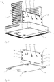
- the light module 1 is shown, wherein the first circuit board 10 and the second circuit board 20 in a housing 5, which also includes a heat sink 7, are installed.
- the heat sink 7 is connected to the second circuit board 20.
- heat can also be absorbed by the heat sink 7, which heat is emitted from the first circuit board 10 to the connected housing 5 and is emitted via the heat sink 7.
- the light sources 21-23 can be seen on the second printed circuit board 20.
- Fig. 2 shows an arrangement with the first and second circuit boards 10, 20 without the housing.
- the first circuit board 10 has mounting holes 60-63.
- the light sources 21-23 can be seen on the second circuit board 20, which also has mounting holes 70-76.
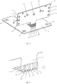
- FIG. 3 is again the previous arrangement with two printed circuit boards 10, 20 of the light module 1, which are interconnected via spring contact elements 30-35 shown.
- a detail view in the Fig. 4 shows an enlarged section with the spring contact elements 30-35, which each include the holder 50 and the spring-mounted pin 40. The pin 40 rests on a contact surface 11.
- FIG. 5 the first and second printed circuit board 10, 20 of the headlamp 1 are illustrated, the illustration simplifying the first and second printed circuit boards 10, 20 in FIG the final orientation is normal to each other, however, the first and second circuit boards 10, 20 are not connected to each other. As a result, the assignment of the spring contact elements 30-35, or of the respective pin 40 to the contact surfaces 11-16 should be illustrated.
- conductor tracks 17 are shown, which are intended to indicate the electrical connection to a driver circuit.
- the driver circuit is not shown for ease of illustration, but is included in the first circuit board 10.
- Fig. 6 shows the light module 1 with the housing 5, which has a window 6 between the space for the first circuit board 10 and the space for the second circuit board 20.
- an electromagnetic shield with a window 6 is arranged between the first printed circuit board 10 and the second printed circuit board 20.
- the electromagnetic shielding is thus formed by at least part of the housing 5 of the light module 1.
- the housing has 5 mounting devices 81-86, wherein the mounting devices 82 and 85 are each designed as centering pins.
- Fig. 6 shows the light module 1 in a first state in which the first and second circuit boards 10, 20 are not yet inserted into the housing.
- Fig. 7 shows the light module 1 in a second state in which the second circuit board 20 is inserted into the housing 5.
- the centering pins 82, 85 are arranged to cooperate with corresponding openings 72 and 75 on the second circuit board 20.
- Fig. 8 shows the light module 1 in a third state, in which the first circuit board 10 is inserted into the housing 5.
- the spring contact elements 30-35 electrically connect the first and second printed circuit boards 10, 20.
- the light sources 21-23 are in the Fig. 6-8 not shown.
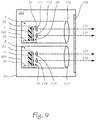
- Fig. 9 schematically shows a motor vehicle headlamp 100 according to the invention with two light modules 1 and 2.
- the light modules 1 and 2 are designed identical in terms of the circuit board assembly, that is, they each have first and second circuit boards 10 and 20 with respective light sources.
- downstream optical elements in the form of optical lenses 110-115 can be designed differently and can thus form different light distributions of a light emitted by the light sources.
- the headlight 100 has a headlight housing 101 in which the two light modules 1, 2 are housed in respective light module housings 102, 103.
- An optically transparent cover 104 is configured to transmit and emit light emitted from the light sources in the form of light beams 121-124.
- the piggyback 100 mounted in a vehicle is configured to illuminate a lane in front of the vehicle.
Landscapes
- Engineering & Computer Science (AREA)
- General Engineering & Computer Science (AREA)
- Microelectronics & Electronic Packaging (AREA)
- Mechanical Engineering (AREA)
- Manufacturing & Machinery (AREA)
- Physics & Mathematics (AREA)
- Optics & Photonics (AREA)
- Non-Portable Lighting Devices Or Systems Thereof (AREA)
- Arrangement Of Elements, Cooling, Sealing, Or The Like Of Lighting Devices (AREA)
Priority Applications (5)
| Application Number | Priority Date | Filing Date | Title |
|---|---|---|---|
| EP17204004.0A EP3489082B1 (fr) | 2017-11-28 | 2017-11-28 | Module lumineux et phare de véhicule |
| PCT/EP2018/077729 WO2019105639A1 (fr) | 2017-11-28 | 2018-10-11 | Module d'éclairage et phare de véhicule |
| KR2020217000080U KR20210002770U (ko) | 2017-11-28 | 2018-10-11 | 광 모듈 및 차량 헤드램프 |
| KR1020207016893A KR20200089288A (ko) | 2017-11-28 | 2018-10-11 | 광 모듈 및 차량 헤드램프 |
| CN201880076672.7A CN111372815B (zh) | 2017-11-28 | 2018-10-11 | 照明模块和车辆头灯 |
Applications Claiming Priority (1)
| Application Number | Priority Date | Filing Date | Title |
|---|---|---|---|
| EP17204004.0A EP3489082B1 (fr) | 2017-11-28 | 2017-11-28 | Module lumineux et phare de véhicule |
Publications (2)
| Publication Number | Publication Date |
|---|---|
| EP3489082A1 true EP3489082A1 (fr) | 2019-05-29 |
| EP3489082B1 EP3489082B1 (fr) | 2021-10-06 |
Family
ID=60629418
Family Applications (1)
| Application Number | Title | Priority Date | Filing Date |
|---|---|---|---|
| EP17204004.0A Active EP3489082B1 (fr) | 2017-11-28 | 2017-11-28 | Module lumineux et phare de véhicule |
Country Status (4)
| Country | Link |
|---|---|
| EP (1) | EP3489082B1 (fr) |
| KR (2) | KR20200089288A (fr) |
| CN (1) | CN111372815B (fr) |
| WO (1) | WO2019105639A1 (fr) |
Cited By (5)
| Publication number | Priority date | Publication date | Assignee | Title |
|---|---|---|---|---|
| WO2022078556A1 (fr) * | 2020-10-13 | 2022-04-21 | Continental Automotive Gmbh | Procédé de fabrication d'un ensemble carte de circuit imprimé et connecteur |
| US11664615B2 (en) * | 2018-08-07 | 2023-05-30 | Tyco Electronics Japan G.K. | Circuit board having terminal, and circuit board assembly |
| GB2616024A (en) * | 2022-02-23 | 2023-08-30 | Arrival Ltd | A hinge and a joining method |
| EP4431795A1 (fr) * | 2023-03-14 | 2024-09-18 | Valeo Vision | Dispositif lumineux d'automobile comprenant des moyens de fixation pour connecter un connecteur à un substrat |
| US12613019B2 (en) | 2022-09-07 | 2026-04-28 | Koito Manufacturing Co., Ltd. | Vehicle lamp |
Families Citing this family (3)
| Publication number | Priority date | Publication date | Assignee | Title |
|---|---|---|---|---|
| DE102021131126A1 (de) | 2021-11-26 | 2023-06-01 | Delo Industrie Klebstoffe Gmbh & Co. Kgaa | Leuchtenbaugruppe und Verfahren zur Herstellung einer Leuchtenbaugruppe |
| DE102023115394A1 (de) * | 2023-06-13 | 2024-12-19 | Cariad Se | Leiterplattensystem anschliessbar an eine gekapselte kühlung |
| DE102024118169A1 (de) * | 2024-06-27 | 2025-12-31 | Osram Gmbh | Leuchtmodul mit verbesserter emv abschirmung |
Citations (6)
| Publication number | Priority date | Publication date | Assignee | Title |
|---|---|---|---|---|
| DE29910417U1 (de) * | 1999-06-15 | 1999-08-12 | Sidler GmbH & Co, 72072 Tübingen | Reflektorleuchte |
| US6231219B1 (en) * | 1999-03-03 | 2001-05-15 | Kurt L. Lohss | Dual-purpose glovebox light assembly and cradle therefor |
| WO2006066530A1 (fr) * | 2004-12-22 | 2006-06-29 | Patent-Treuhand- Gesellschaft Für Elektrische Glühlampen Mbh | Dispositif d'eclairage dote d'au moins une diode electroluminescente et phare de vehicule |
| EP2781826A1 (fr) * | 2013-03-18 | 2014-09-24 | Valeo Vision | Dispositif de signalisation et/ou d'éclairage pour véhicules automobiles |
| US20150229057A1 (en) * | 2014-02-10 | 2015-08-13 | Advanced-Connectek Inc. | Electrical connector with one-piece terminals |
| US20160273751A1 (en) * | 2014-09-30 | 2016-09-22 | General Electric Company | Connector and led lighting device including the connector |
Family Cites Families (1)
| Publication number | Priority date | Publication date | Assignee | Title |
|---|---|---|---|---|
| JP6118474B1 (ja) * | 2014-03-27 | 2017-04-19 | フィリップス ライティング ホールディング ビー ヴィ | 効率的な基板対基板接続 |
-
2017
- 2017-11-28 EP EP17204004.0A patent/EP3489082B1/fr active Active
-
2018
- 2018-10-11 WO PCT/EP2018/077729 patent/WO2019105639A1/fr not_active Ceased
- 2018-10-11 CN CN201880076672.7A patent/CN111372815B/zh active Active
- 2018-10-11 KR KR1020207016893A patent/KR20200089288A/ko not_active Withdrawn
- 2018-10-11 KR KR2020217000080U patent/KR20210002770U/ko not_active Ceased
Patent Citations (6)
| Publication number | Priority date | Publication date | Assignee | Title |
|---|---|---|---|---|
| US6231219B1 (en) * | 1999-03-03 | 2001-05-15 | Kurt L. Lohss | Dual-purpose glovebox light assembly and cradle therefor |
| DE29910417U1 (de) * | 1999-06-15 | 1999-08-12 | Sidler GmbH & Co, 72072 Tübingen | Reflektorleuchte |
| WO2006066530A1 (fr) * | 2004-12-22 | 2006-06-29 | Patent-Treuhand- Gesellschaft Für Elektrische Glühlampen Mbh | Dispositif d'eclairage dote d'au moins une diode electroluminescente et phare de vehicule |
| EP2781826A1 (fr) * | 2013-03-18 | 2014-09-24 | Valeo Vision | Dispositif de signalisation et/ou d'éclairage pour véhicules automobiles |
| US20150229057A1 (en) * | 2014-02-10 | 2015-08-13 | Advanced-Connectek Inc. | Electrical connector with one-piece terminals |
| US20160273751A1 (en) * | 2014-09-30 | 2016-09-22 | General Electric Company | Connector and led lighting device including the connector |
Cited By (6)
| Publication number | Priority date | Publication date | Assignee | Title |
|---|---|---|---|---|
| US11664615B2 (en) * | 2018-08-07 | 2023-05-30 | Tyco Electronics Japan G.K. | Circuit board having terminal, and circuit board assembly |
| WO2022078556A1 (fr) * | 2020-10-13 | 2022-04-21 | Continental Automotive Gmbh | Procédé de fabrication d'un ensemble carte de circuit imprimé et connecteur |
| US12548928B2 (en) | 2020-10-13 | 2026-02-10 | Aumovio Germany Gmbh | Circuit-board-and-connector assembly and a method of producing thereof |
| GB2616024A (en) * | 2022-02-23 | 2023-08-30 | Arrival Ltd | A hinge and a joining method |
| US12613019B2 (en) | 2022-09-07 | 2026-04-28 | Koito Manufacturing Co., Ltd. | Vehicle lamp |
| EP4431795A1 (fr) * | 2023-03-14 | 2024-09-18 | Valeo Vision | Dispositif lumineux d'automobile comprenant des moyens de fixation pour connecter un connecteur à un substrat |
Also Published As
| Publication number | Publication date |
|---|---|
| WO2019105639A1 (fr) | 2019-06-06 |
| KR20210002770U (ko) | 2021-12-10 |
| KR20200089288A (ko) | 2020-07-24 |
| EP3489082B1 (fr) | 2021-10-06 |
| CN111372815A (zh) | 2020-07-03 |
| CN111372815B (zh) | 2023-07-04 |
Similar Documents
| Publication | Publication Date | Title |
|---|---|---|
| EP3489082B1 (fr) | Module lumineux et phare de véhicule | |
| DE4243175B4 (de) | Beleuchtungseinrichtung | |
| DE102008000582A1 (de) | LED-Verbindungsfederbügelbauteil | |
| DE102013225411A1 (de) | Verbinder für eine LED-Modulplatine | |
| DE102018117378A1 (de) | Leistungsversorgung, Lampe, bewegliche Vorrichtung und Verfahren zur Herstellung einer Leistungsversorgung | |
| DE102008040460A1 (de) | In LED-Verbindungseinheit integrierte Verbindungsstückhalterung | |
| DE102008031262A1 (de) | Beleuchtungseinheit für Fahrzeugscheinwerfer und Fahrzeugscheinwerfer | |
| WO2010054924A1 (fr) | Dispositif d'éclairage avec deux cartes de circuits | |
| DE102020107131B4 (de) | Leistungselektronikeinheit und Kraftfahrzeug | |
| EP2938170A1 (fr) | Support pour diode lumineuse SMD | |
| WO2015007904A1 (fr) | Dispositif d'éclairage muni d'une source lumineuse à semi-conducteurs et d'une carte de commande | |
| DE102012218538A1 (de) | Verfahren zur Herstellung einer Lichterzeugungseinheit | |
| DE102011051153A1 (de) | Elektrische Verbindungsvorrichtung für elektrische Komponenten | |
| DE202009018077U1 (de) | Leistungselektronikanordnung | |
| DE102014202196B3 (de) | Leiterplatte und Schaltungsanordnung | |
| DE102017105997A1 (de) | Sendeeinrichtung für eine optische Erfassungseinrichtung eines Kraftfahrzeugs mit einem spezifischen Vormontagemodul, optische Erfassungseinrichtung sowie Kraftfahrzeug | |
| WO2012135878A1 (fr) | Dispositif de fixation et de mise en contact d'une lampe et/ou d'un module lumineux, ainsi que luminaire | |
| DE102017204251A1 (de) | Elektronische steuereinheit und verfahren zum herstellen derselben | |
| DE102021119765B4 (de) | Lichtmodul und Kraftfahrzeugbeleuchtungseinrichtung | |
| DE102014109220A1 (de) | Leiterplattenverbindungselement | |
| DE102020100742B4 (de) | Lichtmodul, Beleuchtungseinrichtung und Kraftfahrzeug | |
| AT513328B1 (de) | Beleuchtungsvorrichtung | |
| EP4207956A1 (fr) | Module de phare de véhicule | |
| EP1968365B1 (fr) | Plaquette munie d'un socle angulé | |
| DE102012106476A1 (de) | Leiterplattenstecker und Leiterplatte |
Legal Events
| Date | Code | Title | Description |
|---|---|---|---|
| PUAI | Public reference made under article 153(3) epc to a published international application that has entered the european phase |
Free format text: ORIGINAL CODE: 0009012 |
|
| STAA | Information on the status of an ep patent application or granted ep patent |
Free format text: STATUS: THE APPLICATION HAS BEEN PUBLISHED |
|
| AK | Designated contracting states |
Kind code of ref document: A1 Designated state(s): AL AT BE BG CH CY CZ DE DK EE ES FI FR GB GR HR HU IE IS IT LI LT LU LV MC MK MT NL NO PL PT RO RS SE SI SK SM TR |
|
| AX | Request for extension of the european patent |
Extension state: BA ME |
|
| STAA | Information on the status of an ep patent application or granted ep patent |
Free format text: STATUS: REQUEST FOR EXAMINATION WAS MADE |
|
| 17P | Request for examination filed |
Effective date: 20191029 |
|
| RBV | Designated contracting states (corrected) |
Designated state(s): AL AT BE BG CH CY CZ DE DK EE ES FI FR GB GR HR HU IE IS IT LI LT LU LV MC MK MT NL NO PL PT RO RS SE SI SK SM TR |
|
| STAA | Information on the status of an ep patent application or granted ep patent |
Free format text: STATUS: EXAMINATION IS IN PROGRESS |
|
| 17Q | First examination report despatched |
Effective date: 20210423 |
|
| GRAP | Despatch of communication of intention to grant a patent |
Free format text: ORIGINAL CODE: EPIDOSNIGR1 |
|
| STAA | Information on the status of an ep patent application or granted ep patent |
Free format text: STATUS: GRANT OF PATENT IS INTENDED |
|
| INTG | Intention to grant announced |
Effective date: 20210716 |
|
| GRAS | Grant fee paid |
Free format text: ORIGINAL CODE: EPIDOSNIGR3 |
|
| GRAA | (expected) grant |
Free format text: ORIGINAL CODE: 0009210 |
|
| STAA | Information on the status of an ep patent application or granted ep patent |
Free format text: STATUS: THE PATENT HAS BEEN GRANTED |
|
| AK | Designated contracting states |
Kind code of ref document: B1 Designated state(s): AL AT BE BG CH CY CZ DE DK EE ES FI FR GB GR HR HU IE IS IT LI LT LU LV MC MK MT NL NO PL PT RO RS SE SI SK SM TR |
|
| REG | Reference to a national code |
Ref country code: GB Ref legal event code: FG4D Free format text: NOT ENGLISH |
|
| REG | Reference to a national code |
Ref country code: CH Ref legal event code: EP Ref country code: AT Ref legal event code: REF Ref document number: 1435946 Country of ref document: AT Kind code of ref document: T Effective date: 20211015 |
|
| REG | Reference to a national code |
Ref country code: DE Ref legal event code: R096 Ref document number: 502017011653 Country of ref document: DE |
|
| REG | Reference to a national code |
Ref country code: IE Ref legal event code: FG4D Free format text: LANGUAGE OF EP DOCUMENT: GERMAN |
|
| REG | Reference to a national code |
Ref country code: LT Ref legal event code: MG9D |
|
| REG | Reference to a national code |
Ref country code: NL Ref legal event code: MP Effective date: 20211006 |
|
| PG25 | Lapsed in a contracting state [announced via postgrant information from national office to epo] |
Ref country code: RS Free format text: LAPSE BECAUSE OF FAILURE TO SUBMIT A TRANSLATION OF THE DESCRIPTION OR TO PAY THE FEE WITHIN THE PRESCRIBED TIME-LIMIT Effective date: 20211006 Ref country code: LT Free format text: LAPSE BECAUSE OF FAILURE TO SUBMIT A TRANSLATION OF THE DESCRIPTION OR TO PAY THE FEE WITHIN THE PRESCRIBED TIME-LIMIT Effective date: 20211006 Ref country code: FI Free format text: LAPSE BECAUSE OF FAILURE TO SUBMIT A TRANSLATION OF THE DESCRIPTION OR TO PAY THE FEE WITHIN THE PRESCRIBED TIME-LIMIT Effective date: 20211006 Ref country code: BG Free format text: LAPSE BECAUSE OF FAILURE TO SUBMIT A TRANSLATION OF THE DESCRIPTION OR TO PAY THE FEE WITHIN THE PRESCRIBED TIME-LIMIT Effective date: 20220106 |
|
| PG25 | Lapsed in a contracting state [announced via postgrant information from national office to epo] |
Ref country code: IS Free format text: LAPSE BECAUSE OF FAILURE TO SUBMIT A TRANSLATION OF THE DESCRIPTION OR TO PAY THE FEE WITHIN THE PRESCRIBED TIME-LIMIT Effective date: 20220206 Ref country code: SE Free format text: LAPSE BECAUSE OF FAILURE TO SUBMIT A TRANSLATION OF THE DESCRIPTION OR TO PAY THE FEE WITHIN THE PRESCRIBED TIME-LIMIT Effective date: 20211006 Ref country code: PT Free format text: LAPSE BECAUSE OF FAILURE TO SUBMIT A TRANSLATION OF THE DESCRIPTION OR TO PAY THE FEE WITHIN THE PRESCRIBED TIME-LIMIT Effective date: 20220207 Ref country code: PL Free format text: LAPSE BECAUSE OF FAILURE TO SUBMIT A TRANSLATION OF THE DESCRIPTION OR TO PAY THE FEE WITHIN THE PRESCRIBED TIME-LIMIT Effective date: 20211006 Ref country code: NO Free format text: LAPSE BECAUSE OF FAILURE TO SUBMIT A TRANSLATION OF THE DESCRIPTION OR TO PAY THE FEE WITHIN THE PRESCRIBED TIME-LIMIT Effective date: 20220106 Ref country code: NL Free format text: LAPSE BECAUSE OF FAILURE TO SUBMIT A TRANSLATION OF THE DESCRIPTION OR TO PAY THE FEE WITHIN THE PRESCRIBED TIME-LIMIT Effective date: 20211006 Ref country code: LV Free format text: LAPSE BECAUSE OF FAILURE TO SUBMIT A TRANSLATION OF THE DESCRIPTION OR TO PAY THE FEE WITHIN THE PRESCRIBED TIME-LIMIT Effective date: 20211006 Ref country code: HR Free format text: LAPSE BECAUSE OF FAILURE TO SUBMIT A TRANSLATION OF THE DESCRIPTION OR TO PAY THE FEE WITHIN THE PRESCRIBED TIME-LIMIT Effective date: 20211006 Ref country code: GR Free format text: LAPSE BECAUSE OF FAILURE TO SUBMIT A TRANSLATION OF THE DESCRIPTION OR TO PAY THE FEE WITHIN THE PRESCRIBED TIME-LIMIT Effective date: 20220107 Ref country code: ES Free format text: LAPSE BECAUSE OF FAILURE TO SUBMIT A TRANSLATION OF THE DESCRIPTION OR TO PAY THE FEE WITHIN THE PRESCRIBED TIME-LIMIT Effective date: 20211006 |
|
| REG | Reference to a national code |
Ref country code: CH Ref legal event code: PL |
|
| REG | Reference to a national code |
Ref country code: DE Ref legal event code: R097 Ref document number: 502017011653 Country of ref document: DE |
|
| PG25 | Lapsed in a contracting state [announced via postgrant information from national office to epo] |
Ref country code: SM Free format text: LAPSE BECAUSE OF FAILURE TO SUBMIT A TRANSLATION OF THE DESCRIPTION OR TO PAY THE FEE WITHIN THE PRESCRIBED TIME-LIMIT Effective date: 20211006 Ref country code: SK Free format text: LAPSE BECAUSE OF FAILURE TO SUBMIT A TRANSLATION OF THE DESCRIPTION OR TO PAY THE FEE WITHIN THE PRESCRIBED TIME-LIMIT Effective date: 20211006 Ref country code: RO Free format text: LAPSE BECAUSE OF FAILURE TO SUBMIT A TRANSLATION OF THE DESCRIPTION OR TO PAY THE FEE WITHIN THE PRESCRIBED TIME-LIMIT Effective date: 20211006 Ref country code: MC Free format text: LAPSE BECAUSE OF FAILURE TO SUBMIT A TRANSLATION OF THE DESCRIPTION OR TO PAY THE FEE WITHIN THE PRESCRIBED TIME-LIMIT Effective date: 20211006 Ref country code: LU Free format text: LAPSE BECAUSE OF NON-PAYMENT OF DUE FEES Effective date: 20211128 Ref country code: EE Free format text: LAPSE BECAUSE OF FAILURE TO SUBMIT A TRANSLATION OF THE DESCRIPTION OR TO PAY THE FEE WITHIN THE PRESCRIBED TIME-LIMIT Effective date: 20211006 Ref country code: DK Free format text: LAPSE BECAUSE OF FAILURE TO SUBMIT A TRANSLATION OF THE DESCRIPTION OR TO PAY THE FEE WITHIN THE PRESCRIBED TIME-LIMIT Effective date: 20211006 Ref country code: CZ Free format text: LAPSE BECAUSE OF FAILURE TO SUBMIT A TRANSLATION OF THE DESCRIPTION OR TO PAY THE FEE WITHIN THE PRESCRIBED TIME-LIMIT Effective date: 20211006 Ref country code: BE Free format text: LAPSE BECAUSE OF NON-PAYMENT OF DUE FEES Effective date: 20211130 |
|
| REG | Reference to a national code |
Ref country code: BE Ref legal event code: MM Effective date: 20211130 |
|
| PLBE | No opposition filed within time limit |
Free format text: ORIGINAL CODE: 0009261 |
|
| STAA | Information on the status of an ep patent application or granted ep patent |
Free format text: STATUS: NO OPPOSITION FILED WITHIN TIME LIMIT |
|
| PG25 | Lapsed in a contracting state [announced via postgrant information from national office to epo] |
Ref country code: LI Free format text: LAPSE BECAUSE OF NON-PAYMENT OF DUE FEES Effective date: 20211130 Ref country code: CH Free format text: LAPSE BECAUSE OF NON-PAYMENT OF DUE FEES Effective date: 20211130 |
|
| 26N | No opposition filed |
Effective date: 20220707 |
|
| GBPC | Gb: european patent ceased through non-payment of renewal fee |
Effective date: 20220106 |
|
| PG25 | Lapsed in a contracting state [announced via postgrant information from national office to epo] |
Ref country code: IE Free format text: LAPSE BECAUSE OF NON-PAYMENT OF DUE FEES Effective date: 20211128 Ref country code: GB Free format text: LAPSE BECAUSE OF NON-PAYMENT OF DUE FEES Effective date: 20220106 Ref country code: AL Free format text: LAPSE BECAUSE OF FAILURE TO SUBMIT A TRANSLATION OF THE DESCRIPTION OR TO PAY THE FEE WITHIN THE PRESCRIBED TIME-LIMIT Effective date: 20211006 |
|
| PG25 | Lapsed in a contracting state [announced via postgrant information from national office to epo] |
Ref country code: SI Free format text: LAPSE BECAUSE OF FAILURE TO SUBMIT A TRANSLATION OF THE DESCRIPTION OR TO PAY THE FEE WITHIN THE PRESCRIBED TIME-LIMIT Effective date: 20211006 |
|
| PG25 | Lapsed in a contracting state [announced via postgrant information from national office to epo] |
Ref country code: IT Free format text: LAPSE BECAUSE OF FAILURE TO SUBMIT A TRANSLATION OF THE DESCRIPTION OR TO PAY THE FEE WITHIN THE PRESCRIBED TIME-LIMIT Effective date: 20211006 |
|
| PG25 | Lapsed in a contracting state [announced via postgrant information from national office to epo] |
Ref country code: CY Free format text: LAPSE BECAUSE OF FAILURE TO SUBMIT A TRANSLATION OF THE DESCRIPTION OR TO PAY THE FEE WITHIN THE PRESCRIBED TIME-LIMIT Effective date: 20211006 |
|
| P01 | Opt-out of the competence of the unified patent court (upc) registered |
Effective date: 20230528 |
|
| PG25 | Lapsed in a contracting state [announced via postgrant information from national office to epo] |
Ref country code: HU Free format text: LAPSE BECAUSE OF FAILURE TO SUBMIT A TRANSLATION OF THE DESCRIPTION OR TO PAY THE FEE WITHIN THE PRESCRIBED TIME-LIMIT; INVALID AB INITIO Effective date: 20171128 |
|
| REG | Reference to a national code |
Ref country code: AT Ref legal event code: MM01 Ref document number: 1435946 Country of ref document: AT Kind code of ref document: T Effective date: 20221128 |
|
| PG25 | Lapsed in a contracting state [announced via postgrant information from national office to epo] |
Ref country code: AT Free format text: LAPSE BECAUSE OF NON-PAYMENT OF DUE FEES Effective date: 20221128 |
|
| PG25 | Lapsed in a contracting state [announced via postgrant information from national office to epo] |
Ref country code: MK Free format text: LAPSE BECAUSE OF FAILURE TO SUBMIT A TRANSLATION OF THE DESCRIPTION OR TO PAY THE FEE WITHIN THE PRESCRIBED TIME-LIMIT Effective date: 20211006 |
|
| PG25 | Lapsed in a contracting state [announced via postgrant information from national office to epo] |
Ref country code: TR Free format text: LAPSE BECAUSE OF FAILURE TO SUBMIT A TRANSLATION OF THE DESCRIPTION OR TO PAY THE FEE WITHIN THE PRESCRIBED TIME-LIMIT Effective date: 20211006 |
|
| PG25 | Lapsed in a contracting state [announced via postgrant information from national office to epo] |
Ref country code: MT Free format text: LAPSE BECAUSE OF FAILURE TO SUBMIT A TRANSLATION OF THE DESCRIPTION OR TO PAY THE FEE WITHIN THE PRESCRIBED TIME-LIMIT Effective date: 20211006 |
|
| REG | Reference to a national code |
Ref country code: DE Ref legal event code: R084 Ref document number: 502017011653 Country of ref document: DE |
|
| PGFP | Annual fee paid to national office [announced via postgrant information from national office to epo] |
Ref country code: DE Payment date: 20251118 Year of fee payment: 9 |
|
| PGFP | Annual fee paid to national office [announced via postgrant information from national office to epo] |
Ref country code: FR Payment date: 20251120 Year of fee payment: 9 |