EP3489744B1 - Anzeigegerät - Google Patents
Anzeigegerät Download PDFInfo
- Publication number
- EP3489744B1 EP3489744B1 EP19151492.6A EP19151492A EP3489744B1 EP 3489744 B1 EP3489744 B1 EP 3489744B1 EP 19151492 A EP19151492 A EP 19151492A EP 3489744 B1 EP3489744 B1 EP 3489744B1
- Authority
- EP
- European Patent Office
- Prior art keywords
- light emitting
- emitting diode
- display
- display device
- face
- Prior art date
- Legal status (The legal status is an assumption and is not a legal conclusion. Google has not performed a legal analysis and makes no representation as to the accuracy of the status listed.)
- Active
Links
Images




Classifications
-
- G—PHYSICS
- G02—OPTICS
- G02F—OPTICAL DEVICES OR ARRANGEMENTS FOR THE CONTROL OF LIGHT BY MODIFICATION OF THE OPTICAL PROPERTIES OF THE MEDIA OF THE ELEMENTS INVOLVED THEREIN; NON-LINEAR OPTICS; FREQUENCY-CHANGING OF LIGHT; OPTICAL LOGIC ELEMENTS; OPTICAL ANALOGUE/DIGITAL CONVERTERS
- G02F1/00—Devices or arrangements for the control of the intensity, colour, phase, polarisation or direction of light arriving from an independent light source, e.g. switching, gating or modulating; Non-linear optics
- G02F1/01—Devices or arrangements for the control of the intensity, colour, phase, polarisation or direction of light arriving from an independent light source, e.g. switching, gating or modulating; Non-linear optics for the control of the intensity, phase, polarisation or colour
- G02F1/13—Devices or arrangements for the control of the intensity, colour, phase, polarisation or direction of light arriving from an independent light source, e.g. switching, gating or modulating; Non-linear optics for the control of the intensity, phase, polarisation or colour based on liquid crystals, e.g. single liquid crystal display cells
- G02F1/133—Constructional arrangements; Operation of liquid crystal cells; Circuit arrangements
- G02F1/1333—Constructional arrangements; Manufacturing methods
- G02F1/1335—Structural association of cells with optical devices, e.g. polarisers or reflectors
- G02F1/1336—Illuminating devices
- G02F1/133602—Direct backlight
- G02F1/133603—Direct backlight with LEDs
-
- H—ELECTRICITY
- H10—SEMICONDUCTOR DEVICES; ELECTRIC SOLID-STATE DEVICES NOT OTHERWISE PROVIDED FOR
- H10H—INORGANIC LIGHT-EMITTING SEMICONDUCTOR DEVICES HAVING POTENTIAL BARRIERS
- H10H20/00—Individual inorganic light-emitting semiconductor devices having potential barriers, e.g. light-emitting diodes [LED]
- H10H20/80—Constructional details
- H10H20/85—Packages
- H10H20/855—Optical field-shaping means, e.g. lenses
- H10H20/856—Reflecting means
-
- G—PHYSICS
- G02—OPTICS
- G02B—OPTICAL ELEMENTS, SYSTEMS OR APPARATUS
- G02B6/00—Light guides; Structural details of arrangements comprising light guides and other optical elements, e.g. couplings
- G02B6/0001—Light guides; Structural details of arrangements comprising light guides and other optical elements, e.g. couplings specially adapted for lighting devices or systems
- G02B6/0011—Light guides; Structural details of arrangements comprising light guides and other optical elements, e.g. couplings specially adapted for lighting devices or systems the light guides being planar or of plate-like form
- G02B6/0033—Means for improving the coupling-out of light from the light guide
- G02B6/0035—Means for improving the coupling-out of light from the light guide provided on the surface of the light guide or in the bulk of it
- G02B6/0045—Means for improving the coupling-out of light from the light guide provided on the surface of the light guide or in the bulk of it by shaping at least a portion of the light guide
-
- G—PHYSICS
- G02—OPTICS
- G02F—OPTICAL DEVICES OR ARRANGEMENTS FOR THE CONTROL OF LIGHT BY MODIFICATION OF THE OPTICAL PROPERTIES OF THE MEDIA OF THE ELEMENTS INVOLVED THEREIN; NON-LINEAR OPTICS; FREQUENCY-CHANGING OF LIGHT; OPTICAL LOGIC ELEMENTS; OPTICAL ANALOGUE/DIGITAL CONVERTERS
- G02F1/00—Devices or arrangements for the control of the intensity, colour, phase, polarisation or direction of light arriving from an independent light source, e.g. switching, gating or modulating; Non-linear optics
- G02F1/01—Devices or arrangements for the control of the intensity, colour, phase, polarisation or direction of light arriving from an independent light source, e.g. switching, gating or modulating; Non-linear optics for the control of the intensity, phase, polarisation or colour
- G02F1/13—Devices or arrangements for the control of the intensity, colour, phase, polarisation or direction of light arriving from an independent light source, e.g. switching, gating or modulating; Non-linear optics for the control of the intensity, phase, polarisation or colour based on liquid crystals, e.g. single liquid crystal display cells
- G02F1/133—Constructional arrangements; Operation of liquid crystal cells; Circuit arrangements
- G02F1/1333—Constructional arrangements; Manufacturing methods
- G02F1/1335—Structural association of cells with optical devices, e.g. polarisers or reflectors
- G02F1/133553—Reflecting elements
-
- G—PHYSICS
- G02—OPTICS
- G02F—OPTICAL DEVICES OR ARRANGEMENTS FOR THE CONTROL OF LIGHT BY MODIFICATION OF THE OPTICAL PROPERTIES OF THE MEDIA OF THE ELEMENTS INVOLVED THEREIN; NON-LINEAR OPTICS; FREQUENCY-CHANGING OF LIGHT; OPTICAL LOGIC ELEMENTS; OPTICAL ANALOGUE/DIGITAL CONVERTERS
- G02F1/00—Devices or arrangements for the control of the intensity, colour, phase, polarisation or direction of light arriving from an independent light source, e.g. switching, gating or modulating; Non-linear optics
- G02F1/01—Devices or arrangements for the control of the intensity, colour, phase, polarisation or direction of light arriving from an independent light source, e.g. switching, gating or modulating; Non-linear optics for the control of the intensity, phase, polarisation or colour
- G02F1/13—Devices or arrangements for the control of the intensity, colour, phase, polarisation or direction of light arriving from an independent light source, e.g. switching, gating or modulating; Non-linear optics for the control of the intensity, phase, polarisation or colour based on liquid crystals, e.g. single liquid crystal display cells
- G02F1/133—Constructional arrangements; Operation of liquid crystal cells; Circuit arrangements
- G02F1/1333—Constructional arrangements; Manufacturing methods
- G02F1/1335—Structural association of cells with optical devices, e.g. polarisers or reflectors
- G02F1/1336—Illuminating devices
- G02F1/133602—Direct backlight
- G02F1/133605—Direct backlight including specially adapted reflectors
-
- H—ELECTRICITY
- H05—ELECTRIC TECHNIQUES NOT OTHERWISE PROVIDED FOR
- H05B—ELECTRIC HEATING; ELECTRIC LIGHT SOURCES NOT OTHERWISE PROVIDED FOR; CIRCUIT ARRANGEMENTS FOR ELECTRIC LIGHT SOURCES, IN GENERAL
- H05B33/00—Electroluminescent light sources
- H05B33/02—Details
- H05B33/04—Sealing arrangements, e.g. against humidity
-
- H—ELECTRICITY
- H05—ELECTRIC TECHNIQUES NOT OTHERWISE PROVIDED FOR
- H05B—ELECTRIC HEATING; ELECTRIC LIGHT SOURCES NOT OTHERWISE PROVIDED FOR; CIRCUIT ARRANGEMENTS FOR ELECTRIC LIGHT SOURCES, IN GENERAL
- H05B33/00—Electroluminescent light sources
- H05B33/10—Apparatus or processes specially adapted to the manufacture of electroluminescent light sources
-
- H—ELECTRICITY
- H10—SEMICONDUCTOR DEVICES; ELECTRIC SOLID-STATE DEVICES NOT OTHERWISE PROVIDED FOR
- H10H—INORGANIC LIGHT-EMITTING SEMICONDUCTOR DEVICES HAVING POTENTIAL BARRIERS
- H10H20/00—Individual inorganic light-emitting semiconductor devices having potential barriers, e.g. light-emitting diodes [LED]
- H10H20/80—Constructional details
- H10H20/84—Coatings, e.g. passivation layers or antireflective coatings
- H10H20/841—Reflective coatings, e.g. dielectric Bragg reflectors
-
- H—ELECTRICITY
- H10—SEMICONDUCTOR DEVICES; ELECTRIC SOLID-STATE DEVICES NOT OTHERWISE PROVIDED FOR
- H10H—INORGANIC LIGHT-EMITTING SEMICONDUCTOR DEVICES HAVING POTENTIAL BARRIERS
- H10H20/00—Individual inorganic light-emitting semiconductor devices having potential barriers, e.g. light-emitting diodes [LED]
- H10H20/80—Constructional details
- H10H20/85—Packages
-
- H—ELECTRICITY
- H10—SEMICONDUCTOR DEVICES; ELECTRIC SOLID-STATE DEVICES NOT OTHERWISE PROVIDED FOR
- H10H—INORGANIC LIGHT-EMITTING SEMICONDUCTOR DEVICES HAVING POTENTIAL BARRIERS
- H10H20/00—Individual inorganic light-emitting semiconductor devices having potential barriers, e.g. light-emitting diodes [LED]
- H10H20/80—Constructional details
- H10H20/85—Packages
- H10H20/851—Wavelength conversion means
-
- H—ELECTRICITY
- H10—SEMICONDUCTOR DEVICES; ELECTRIC SOLID-STATE DEVICES NOT OTHERWISE PROVIDED FOR
- H10H—INORGANIC LIGHT-EMITTING SEMICONDUCTOR DEVICES HAVING POTENTIAL BARRIERS
- H10H20/00—Individual inorganic light-emitting semiconductor devices having potential barriers, e.g. light-emitting diodes [LED]
- H10H20/80—Constructional details
- H10H20/85—Packages
- H10H20/852—Encapsulations
- H10H20/853—Encapsulations characterised by their shape
-
- H—ELECTRICITY
- H10—SEMICONDUCTOR DEVICES; ELECTRIC SOLID-STATE DEVICES NOT OTHERWISE PROVIDED FOR
- H10H—INORGANIC LIGHT-EMITTING SEMICONDUCTOR DEVICES HAVING POTENTIAL BARRIERS
- H10H20/00—Individual inorganic light-emitting semiconductor devices having potential barriers, e.g. light-emitting diodes [LED]
- H10H20/80—Constructional details
- H10H20/85—Packages
- H10H20/852—Encapsulations
- H10H20/854—Encapsulations characterised by their material, e.g. epoxy or silicone resins
-
- H—ELECTRICITY
- H10—SEMICONDUCTOR DEVICES; ELECTRIC SOLID-STATE DEVICES NOT OTHERWISE PROVIDED FOR
- H10H—INORGANIC LIGHT-EMITTING SEMICONDUCTOR DEVICES HAVING POTENTIAL BARRIERS
- H10H20/00—Individual inorganic light-emitting semiconductor devices having potential barriers, e.g. light-emitting diodes [LED]
- H10H20/80—Constructional details
- H10H20/81—Bodies
- H10H20/819—Bodies characterised by their shape, e.g. curved or truncated substrates
- H10H20/82—Roughened surfaces, e.g. at the interface between epitaxial layers
-
- H—ELECTRICITY
- H10—SEMICONDUCTOR DEVICES; ELECTRIC SOLID-STATE DEVICES NOT OTHERWISE PROVIDED FOR
- H10H—INORGANIC LIGHT-EMITTING SEMICONDUCTOR DEVICES HAVING POTENTIAL BARRIERS
- H10H20/00—Individual inorganic light-emitting semiconductor devices having potential barriers, e.g. light-emitting diodes [LED]
- H10H20/80—Constructional details
- H10H20/85—Packages
- H10H20/851—Wavelength conversion means
- H10H20/8516—Wavelength conversion means having a non-uniform spatial arrangement or non-uniform concentration, e.g. patterned wavelength conversion layer or wavelength conversion layer with a concentration gradient
-
- H—ELECTRICITY
- H10—SEMICONDUCTOR DEVICES; ELECTRIC SOLID-STATE DEVICES NOT OTHERWISE PROVIDED FOR
- H10W—GENERIC PACKAGES, INTERCONNECTIONS, CONNECTORS OR OTHER CONSTRUCTIONAL DETAILS OF DEVICES COVERED BY CLASS H10
- H10W90/00—Package configurations
Definitions
- the present invention generally relates to a display device. More specifically, the present invention relates to a display device having a light source with a reflective layer.
- a display device includes a light source.
- JP 2006-319371 A discloses a light emitting element with a reflective layer.
- the reflective layer disclosed in JP 2006-319371 A reflects light and is formed between layers of a semiconductor element (LED chip), or on a surface of a sapphire substrate of the semiconductor element.
- WO 2013/038802 A1 and US 2013/0278865 A1 discloses a display device comprising: a display including a display face and configured to display images; at least one light emitting diode configured to emit light; a reflective sheet including a bottom face arranged substantially parallel with the display face and configured to reflect the light emitted by the at least one light emitting diode to the display; an optical sheet arranged substantially parallel with the display face between the display and the reflective sheet, configured to transmit the light emitted by the at least one light emitting diode to the display, and including a diffusion plate and/or a polarizing film configured to diffuse the light emitted by the at least one light emitting diode and/or align the polarization direction of the light emitted by the at least one light emitting diode; and a light source disposition component including a pair of inclined parts and a flat part which connects the inclined parts such that the light source disposition component has a trapezoidal cross-sectional shape, and the inclined parts are protruding from
- US 2015/049510 A1 discloses a flip chip type light emitting diode in which a contact surface between an upper face of the light emitting diode chip and a lower face of a reflective element has an uneven shape and side surfaces of the light emitting diode chip are surrounded by a radiation-transmissive encapsulation comprising luminescence conversion particles, and in which the surface area of the reflective element is larger than the surface area of the light emitting diode chip.
- the reflective layer is formed between the layers of the semiconductor element (LED chip) or on the surface of the sapphire substrate of the semiconductor element.
- the surface area of the reflective layer is formed between the layers of the semiconductor element (LED chip) or on the surface of the sapphire substrate of the semiconductor element.
- One object of the present invention is to provide a display device with which a decrease in the light distribution angle can be suppressed. This object is achieved by the display device defined in the appended claim 1. Further advantageous effects can be obtained by preferred embodiments defined in the appended dependent claims.
- the present invention provides a display device according to the appended claim 1.
- the display device further comprises a wiring board for the at least one light emitting diode, the wiring board being provided between the flat part of the light source disposition component and the at least one light emitting diode.
- the display device further comprises: a heat sink provided between the flat part of the light source disposition component and the at least one light emitting diode.
- the light source disposition component is covered by the reflective sheet.
- the reflective sheet has a pair of inclined parts, the inclined parts of the reflective sheet being provided to be opposite to the pair of inclined parts of the light source disposition component, respectively.
- the at least one light emitting diode includes a plurality of light emitting diodes disposed on the light source disposition component.
- the plurality of light emitting diodes are arranged along a horizontal line on a plane substantially parallel to the display face of the display.
- the plurality of light emitting diodes are arranged along a vertical line on a plane substantially parallel to the display face of the display.
- the plurality of light emitting diodes are arranged in a plurality of lines.
- the at least one light emitting diode is configured to emit light to the display.
- the at least one light emitting diode includes a sapphire substrate, a translucent sealing resin, and a reflective layer that forms an uppermost later of the light emitting diode.
- the surface area (plane area) of the reflective layer can be easily made larger than the surface area (plane area) of the light emitting diode chip.
- a greater proportion of the light emitted from the light emitting diode chip toward the upper side of the light emitting diode chip is reflected to the sides of the light emitting diode chip by the reflective layer. This makes it possible to increase the proportion of the light emitted to the sides of the at least one light emitting diode with respect to the light emitted toward the upper side of the at least one light emitting diode.
- the decrease in the distribution angle of the light from the at least one light emitting diode can be suppressed. Also, by providing the reflective layer and the light emitting diode chip separately, there is no need to take into account the influence of heat generation from the light emitting diode chip and other such factors.
- the material of the reflective layer can be selected from a wide variety of materials. Also, by providing the reflective layer on the sealing resin, the reflective layer can be formed more easily than when the reflective layer and the light emitting diode chip are provided integrally.
- the reflective layer has an outer periphery that is disposed further outside than an outer periphery of the light emitting diode chip as viewed in a direction perpendicular to an upper face of the at least one light emitting diode.
- the light emitted from the light emitting diode chip toward the upper side of the light emitting diode chip can be easily reflected to all four sides of the light emitting diode chip by the reflective layer.
- the decrease in the distribution angle of the light from the at least one light emitting diode can be further suppressed.
- the substrate is disposed at a top of the light emitting diode chip, and an upper face of the substrate and a lower face of the reflective layer are separated by the sealing resin.
- the reflective layer includes a specific pattern that is configured to transmit part of the light from the light emitting diode chip.
- part of the light from the light emitting diode chip can be utilized by transmitting the light to the outside of the at least one light emitting diode through the pattern of the reflection layer (the gaps in the pattern).
- the specific pattern can have a lattice-shape or has a shape in which rectangles are arranged in a specific direction.
- the at least one light emitting diode further includes a phosphor layer that is disposed between the sealing resin and the light emitting diode chip.
- the phosphor layer is disposed on side faces of the light emitting diode chip, and overlaps the reflective layer in a plan view (as viewed in a direction perpendicular to an upper face of the at least one light emitting diode).
- the sealing resin and an upper face of the light emitting diode chip closely contact with each other. With this configuration, the phosphor layer is not disposed on the upper face of the light emitting diode chip, and is disposed only on the side faces of the light emitting diode chip. Thus, the height of the at least one light emitting diode can be reduced.
- the phosphor layer is arranged to surround the side faces of the light emitting diode chip. With this configuration, light traveling from the side faces of the light emitting diode chip can be easily guided into the phosphor layer.
- the sealing resin and side faces of the light emitting diode chip closely contact with each other.
- the at least one light emitting diode can be made smaller.
- the reflective layer is formed substantially flat. With this configuration, the reflective layer can be easily formed.
- the substrate is made of a sapphire substrate.
- the light emitting diode chip includes the sapphire substrate, a first conductivity type GaN layer, a light emitting layer, and a second conductivity type GaN layer that are arranged in this order from an upper face side of the light emitting diode chip.
- a sapphire substrate has excellent light transmittance. Therefore, with a sapphire substrate, the proportion of light absorbed by the substrate can be reduced. Thus, the decrease in emission efficiency of the at least one light emitting diode can be suppressed.
- the display device further comprises a reflective sheet configured to reflect light from the at least one light emitting diode.
- the reflective sheet includes a bottom face that is arranged substantially parallel to a display face of the display.
- the at least one light emitting diode is disposed at a location closer to the display than the bottom face in a direction substantially perpendicular to the display face of the display.
- the at least one light emitting diode includes a plurality of light emitting diodes.
- the light emitting diodes can be arranged along a horizontal line on a plane substantially parallel to a display face of the display.
- the light emitting diodes can be arranged along a vertical line on a plane substantially parallel to a display face of the display.
- the light emitting diodes can be arranged in a plurality of lines.
- the reflective layer has an outer periphery that substantially overlaps with an outer periphery of the sealing resin as viewed in a direction perpendicular to an upper face of the at least one light emitting diode.
- the reflective layer has an upper face that forms an uppermost face of the at least one light emitting diode.
- the substrate has an uneven upper face.
- the sealing resin entirely covers the light emitting diode chip and the phosphor layer.
- the upper face of the sealing resin is exposed to outside through a gap in the reflective layer.
- a display device main body 10a is provided to the display device 10 according to the first to fourth examples not forming part of the present invention.
- the display device main body 10a includes a display component 11 (e.g., display) for displaying images, a reflective sheet 12, an optical sheet 13, and a rear frame 14, which will all be described below.
- the display component 11 includes a liquid crystal cell, for example.
- the display component is configured to display image.
- the left direction is the arrow X1 direction
- the right direction is the arrow X2 direction
- the front direction is the arrow Y1 direction
- the rear direction is the arrow Y2 direction
- the upward direction is the arrow Z1 direction
- the downward direction is the arrow Z2 direction.
- X direction represents the horizontal direction of the display device 10
- Y direction represents front-to-rear direction of the display device 10
- Z direction represents the vertical direction of the display device 10.
- the display device 10 includes an LED element 100 that emits light to the display component 11.
- the display device 10 is configured as a direct-type liquid crystal module that displays video on the display component 11, using as a backlight the LED (light emitting diode) element 100 provided on the arrow Y2 direction side.
- the LED element 100 is an example of the "at least one light source" of the present disclosure.
- the display component 11 is in the form of a plate arranged on a plane parallel to the XZ plane.
- the display component 11 is configured to have a rectangular shape including short sides 11a and 11b (short edges) and long sides 11c and 11d (long edges).
- the display component 11 includes a display face 11e bounded by the short side 11a, the short side 11b, the long side 11c, and the long side 11d.
- the LED element 100 includes an LED chip 100a (see FIG. 3 ). A plurality (ten, for example) of the LED elements 100 are provided, and they are configured to emit light on the side of the display component 11 (the arrow Y1 direction side).
- the LED chip 100a is an example of the "semiconductor element" of the present disclosure.
- the reflective sheet 12 includes a bottom face 12a that is arranged substantially parallel to the display face 11e of the display component 11.
- the display face 11e of the display component 11 is disposed substantially parallel to the optical sheet 13.
- the reflective sheet 12 includes inclined parts 12b to 12e.
- the inclined parts 12b to 12e are inclined to the bottom face 12a and are provided between the bottom face 12a and the outer edges (the short sides 11 a and 11b and the long sides 11c and 11d) of the display component 11.
- the inclined parts 12b to 12e is configured to reflect (and diffuse) light from the LED element 100.
- the reflective sheet 12 is provided between the rear frame 14 and the optical sheet 13.
- the reflective sheet 12 is configured to reflect the light from the LED element 100 to the side of the display component 11 (the arrow Y1 direction side).
- the rear frame 14 is made of metal, for example.
- the rear frame 14 is formed in a concave shape recessed in the arrow Y2 direction.
- the rear frame 14 is attached to the display device 10 from the
- the reflective sheet 12 is made of a resin (preferably PET (polyethylene terephthalate) in a reflective state), for example.
- the reflecting sheet 12 is configured to have a shape that conforms to the rear frame 14 (a concave shape recessed toward the arrow Y2 direction side).
- the bottom face 12a of the reflective sheet 12 is formed to have a rectangular shape on a plane parallel to the XZ plane.
- the inclined parts 12b to 12e of the reflective sheet 12 extends from the edges of the bottom face 12a, respectively, to surround the bottom face 12a.
- the inclined part 12b is provided between the end of the bottom face 12a on the arrow X1 direction side and the short side 11a of the display component 11, and is inclined with respect to the bottom face 12a.
- the inclined part 12c (12d and 12e) is provided between the end of the bottom face 12a and the short side 11b (the long side 11c and the long side 11d) of the display component 11, and is inclined with respect to the bottom face 12a.
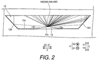
- the LED element 100 is disposed closer to the display component 11 than the bottom face 12a in a direction (Y direction) substantially perpendicular to the display face 11e of the display component 11. More specifically, the display device 10 is provided with a light source disposition component 15 that protrudes from the bottom face 12a toward the display component 11 (Y1 direction side).
- the light source disposition component 15 includes an inclined part 15a provided so as to be opposite to the inclined part 12d, and an inclined part 15b provided so as to be opposite to the inclined part 12e.
- the light source disposition component 15 includes a flat part 15c that connects the end of the inclined part 15a on the Y1 direction side with the end of the inclined part 15b on the Y1 direction side.
- the flat part 15c is provided so as to extend in the X direction.
- Ten LED elements 100 are mounted on the flat part 15c, spaced apart in the X direction.
- a heat sink and a wiring board for the light source are provided between the flat part 15c and the LED elements 100.
- the light source disposition component 15 can be covered by the reflective sheet 12.
- the cross-sectional shape of the light source disposition component 15 is trapezoidal.
- the LED elements 100 disposed on the flat part 15c emit light radially.
- members other than the reflective sheet 12, the light source disposition component 15, and the LED element 100 are omitted for the sake of brevity.
- the broken lines in FIG. 2 are examples of the paths of light emitted from the LED element 100.
- the optical sheet 13 includes a diffusion plate, and/or a polarizing film. As shown in FIG. 1 , the optical sheet 13 is formed in a flat shape extending in a plane parallel to the XZ plane between the display component 11 and the rear frame 14. Consequently, the light emitted from the LED elements 100 irradiates the optical sheet 13. As a result, the light emitted from the LED elements 100 is diffused by the optical sheet 13, and the polarization directions of the light are aligned by the optical sheet 13.
- the optical sheet 13 is not limited to being configured as a single sheet, and can be a combination of a plurality of sheets each having a specific function.
- the display component 11 is configured to display images by changing the transmissivity of the liquid crystal with respect to the light transmitted through the optical sheet 13, or the like.
- the LED element 100 includes the LED chip 100a including the sapphire substrate 1.
- the LED element 100 also includes a translucent sealing resin 2 that covers the LED chip 100a.
- the upper face 2a of the sealing resin 2 is formed substantially flat.
- the LED element 100 includes a reflective layer 3 disposed on the upper face 2a of the sealing resin 2.
- the reflective layer 3 forms an uppermost layer of the LED element 100.
- an upper face of the reflective layer 3 forms an uppermost face of the LED element 100.
- the upper face 2a of the sealing resin 2 is formed to be substantially parallel to the flat part 15c of the light source disposition component 15.
- the sapphire substrate 1 and the upper face 2a are examples of the “substrate” and the “upper face of the sealing resin,” respectively, of the present disclosure.
- the phrase “the upper face 2a is formed substantially flat” is a broad concept encompassing a case in which fine bumps or pits are formed on the upper face 2a of the sealing resin 2.
- the light emitted from the LED chip 100a (a PN junction 5 (discussed below)
- the light emitted toward the upper side of the LED chip 100a is incident on the reflective layer 3, and is reflected to the sides of the LED chip 100a, or to the lower side of the reflective layer 3.
- the lower face 3a of the reflective layer 3 has an uneven shape. More specifically, a plurality of tiny protrusions 3b are disposed on the lower face 3a of the reflective layer 3. The protrusions 3b protrude so as to taper toward the arrow Y2 direction side.
- the lower face 3a is an example of the "lower face of the reflective layer" of the present disclosure.
- the upper face 1a of the sapphire substrate 1 also has an uneven shape. More specifically, a plurality of tiny protrusions 1b are disposed on the upper face 1a of the sapphire substrate 1. In other words, the upper face 1a of the sapphire substrate 1 is formed as an uneven upper face.
- the protrusions 1b protrude toward the arrow Y1 direction side.
- the protrusions 1b are formed by electric discharge machining.
- the upper face 1a is an example of the "upper face of the substrate" of the present disclosure.
- the reflective layer 3 is made of gold. More specifically, the reflective layer 3 is provided by vapor-depositing gold on the upper face 2a of the sealing resin 2.
- the reflective layer 3 is formed substantially flat. More specifically, the reflective layer 3 is configured so that its thickness in the Y direction is substantially constant.
- the phrase "the reflective layer 3 is formed substantially flat" is a broad concept encompassing a case in which fine bumps or pits are formed on the lower face 3a of the reflective layer 3.
- the LED chip 100a includes the sapphire substrate 1, an N-type GaN layer 4, the PN junction 5, and a P-type GaN layer 6 that are disposed in this order starting from the upper face 2a side of the sealing resin 2 (the arrow Y1 direction side). That is, in the LED chip 100a, the sapphire substrate 1 is disposed on the uppermost face. In other words, the sapphire substrate 1 is disposed at a top of the LED chip 100a. That is, the LED chip 100a is a flip chip type. More specifically, the N-type GaN layer 4 is formed under the lower face 1c of the sapphire substrate 1.
- a stepped part 4b extending in the Y direction (as viewed from the X direction) is provided to the lower face 4a of the N-type GaN layer 4.
- a flat face 4c and a flat face 4d are provided to the lower face 4a of the N-type GaN layer 4, with the stepped part 4b as a boundary.
- the flat face 4c is substantially flat and parallel relative to the XZ plane, and extends in the Z2 direction relative to the stepped part 4b.
- the flat face 4d is substantially flat and parallel relative to the XZ plane, and extends in the Z1 direction relative to the stepped part 4b.
- the PN junction 5 is formed under the flat face 4d of the N-type GaN layer 4.
- a negative electrode pad 7 is provided under the flat face 4c of the N-type GaN layer 4.
- the P-type GaN layer 6 is formed under the PN junction 5.
- a positive electrode pad 8 is provided under the P-type GaN layer 6. Also, the positive electrode pad 8 and the negative electrode pad 7 are in contact with (soldered to) and electrically connected to a copper foil (not shown) on the flat part 15c of the light source disposition component 15.
- the PN junction 5 is an example of the "light emitting layer” of the present disclosure.
- the N-type GaN layer 4 and the P-type GaN layer 6 are examples of the "first conductivity type GaN layer" and the "second conductivity type GaN layer,” respectively, of the present disclosure.
- the reflective layer 3 has an outer periphery that is disposed further to the outside than an outer periphery of the LED chip 100a as viewed in a direction perpendicular to an upper face of the LED element 100 or in the Y direction (hereinafter "in the plan view"). More specifically, in the plan view, the reflective layer 3 is configured to have a rectangular shape that includes the short sides 3c (the arrow Z2 direction side) and 3d (the arrow Z1 direction side), and the long sides 3e (the arrow X1 direction side) and 3f (the arrow X2 direction side).
- the sapphire substrate 1 is configured to have a rectangular shape that includes the short sides 1d (the arrow Z2 direction side) and 1e (the arrow Z1 direction side), and the long sides 1f (the arrow X1 direction side) and 1g (the arrow X2 direction side).
- the short side 3c of the reflective layer 3 is provided more on the arrow Z2 direction side than the short side 1d of the sapphire substrate 1, and the short side 3d of the reflective layer 3 is provided more on the arrow Z1 direction side than short side 1e of the sapphire substrate 1.
- the long side 3e of the reflective layer 3 is provided more on the arrow X1 direction side than the long side 1f of the sapphire substrate 1, and the long side 3f of the reflective layer 3 is provided more on the arrow X2 direction side than the long side 1g of the sapphire substrate 1.
- the short side 3c, the short side 3d, the long side 3e, and the long side 3f are examples of "the outer periphery of the reflective layer.”
- the short side 1d, the short side 1e, the long side 1f, and the long side 1g are examples of "the outer periphery of the semiconductor element.”
- the outer periphery of the reflective layer 3 is configured to substantially overlap the outer periphery of the sealing resin 2 (see FIG. 3 ). More specifically, in the plan view, the sealing resin 2 is configured to have a rectangular shape that includes has the short sides 2b (the arrow Z2 direction side) and 2c (the arrow Z1 direction side), and the long sides 2d (the arrow X1 direction side) and 2e (the arrow X2 direction side). Also, in the plan view, the short side 3c of the reflective layer 3 and the short side 2b of the sealing resin 2 substantially overlap. Also, in the plan view, the short side 3d of the reflective layer 3 and the short side 2c of the sealing resin 2 substantially overlap. Also, in the plan view, the long side 3e of the reflective layer 3 and the long side 2d of the sealing resin 2 substantially overlap. Also, in the plan view, the long side 3f of the reflective layer 3 and the long side 2e of the sealing resin 2 substantially overlap.
- the upper face 1a of the sapphire substrate 1 and the lower face 3a of the reflective layer 3 are configured to be separated from each other by the sealing resin 2. More specifically, the entire upper face 1a of the sapphire substrate 1 is covered by the sealing resin 2. Thus, the sapphire substrate 1 (the upper face 1a) does not directly contact with the reflective layer 3 (the lower face 3a).
- the LED element 100 further includes a phosphor layer 9 that is disposed between the sealing resin 2 and the LED chip 100a.
- the phosphor layer 9 is disposed on the side faces of the LED chip 100a.
- the phosphor layer 9 is disposed so as to overlap the reflective layer 3 in the plan view.
- the sealing resin 2 and the upper face 1a of the LED chip 100a (the sapphire substrate 1) closely contact with each other. More specifically, the phosphor layer 9 is disposed so as to cover the entire surface of the LED chip 100a other than the upper face 1a of the sapphire substrate 1.
- the entire phosphor layer 9 is disposed inside the sealing resin 2. Specifically, the sealing resin 2 entirely covers the LED chip 100a and the phosphor layer 9.
- the phosphor layer 9 is arranged to surround the side faces of the LED chip 100a. More specifically, in the plan view, the phosphor layer 9 with a thickness t1 is disposed to closely contact with the short side 1d, the short side 1e, the long side 1f, and the long side 1g of the LED chip 100a (the sapphire substrate 1).
- the display device 10 comprises the display component 11 for displaying images and the LED elements 100 for emitting light at the display component 11.
- the LED elements 100 each include an LED chip 100a.
- the LED chip 100a includes the sapphire substrate 1, the translucent sealing resin 2 that covers the LED chip 100a, and the reflective layer 3 disposed on the upper face 2a of the sealing resin 2.
- the reflective layer 3 is disposed on the upper face 2a of the sealing resin 2 that is provided so as to cover the LED chips 100a.
- the surface area (plane area) of the reflective layer 3 can be easily made larger than the surface area (plane area) of the LED chips 100a.
- the surface area (plane area) of the reflective layer 3 is substantially equal to the surface area (plane area) of the LED chips 100a
- a greater proportion of the light emitted from the LED chips 100a to the upper side of the LED chip 100a is reflected by the reflective layer 3 toward the sides of the LED chips 100a. Consequently, the proportion of the light emitted to the sides of the LED element 100 can be increased with respect to the light emitted to the upper side of the LED element 100.
- the decrease in the distribution angle of the light from the LED element 100 can be suppressed.
- the reflective layer 3 and the LED chip 100a separately, there is no need to take into account the influence of heat generation or the like in the LED chip 100a.
- the material of the reflective layer 3 can be selected from a wider range. Also, by providing the reflective layer 3 on the sealing resin 2, the reflective layer 3 can be formed more easily than when the reflective layer 3 and the LED chip 100a are provided integrally. Note that the phrase "the upper face 2a is formed substantially flat" is a broad concept encompassing a case in which fine bumps or pits are formed on the upper face 2a of the sealing resin 2.
- the display device 10 is configured such that the outer periphery of the reflective layer 3 is disposed more to the outside than the outer periphery of the LED chip 100a in the plan view. Consequently, in the plan view, the region occupied by the reflective layer 3 covers the entire region occupied by the LED chip 100a, and the surface area of the reflective layer 3 is larger than the surface area of the LED chip 100a. As a result, the light emitted from the LED chip 100a to the upper side of the LED chip 100a can be easily reflected by the reflective layer 3 to all four sides of the LED chip 100a.
- the proportion of the light emitted to the sides of the LED element 100 can be further increased with respect to the light emitted to the upper side of the LED element 100.
- the decrease in the distribution angle of the light from the LED element 100 can be further suppressed.
- the display device 10 is configured such that the reflective layer 3 has the outer periphery that substantially overlaps the outer periphery of the sealing resin 2 in the plan view. Consequently, the light passing near the edges of the sealing resin 2 can be reflected by the reflective layer 3. Thus, the light from the LED chip 100a can be easily reflected to the sides of the LED element 100.
- the display device 10 is configured such that the sapphire substrate 1 of the LED chip 100a is disposed on the uppermost surface (at the top of the LED chip 100a), and the upper face 1a of the sapphire substrate 1 and the lower face 3a of the reflective layer 3 are separated from each other by the sealing resin 2. Consequently, there is no need to adjust the height of the sealing resin 2 so that the reflective layer 3 will straddle both the upper face 1a of the sapphire substrate 1 and the upper face 2a of the sealing resin 2 to the side of the sapphire substrate 1. Thus, the LED element 100 can be formed more easily. Also, the sapphire substrate 1 and the reflective layer 3 do not interfere with each other. Thus, degradation of the sapphire substrate 1 and the reflective layer 3 can be suppressed.
- the display device 10 is configured such that the LED element 100 further includes the phosphor layer 9 that is disposed between the sealing resin 2 and the LED chip 100a.
- the phosphor layer 9 is disposed on the side faces of the LED chip 100a, and is disposed so as to overlap the reflective layer 3 in the plan view.
- the sealing resin 2 and the upper face 1a of the LED chip 100a (the sapphire substrate 1) closely contact with each other. Consequently, the phosphor layer 9 is not disposed on the upper face 1a of the LED chip 100a (the sapphire substrate 1), and the phosphor layer 9 is disposed only on the side faces of the LED chip 100a.
- the height of the LED element 100 can be reduced.
- the display device 10 is configured such that the phosphor layer 9 is arranged to surround the side faces of the LED chip 100a. Consequently, the light traveling from the side faces of the LED chip 100a can easily be introduced into the phosphor layer 9.
- the display device 10 is configured such that the lower face 3a of the reflective layer 3 has an uneven shape. Consequently, the light emitted from the LED chip 100a and incident on the lower face 3a of the reflective layer 3 is diffused by the convex and the concave (or the texturing) on the reflective layer 3. Thus, the proportion of the light reflected to the sides of the LED chip 100a can be effectively increased.
- the display device 10 is configured such that the upper face 1a of the sapphire substrate 1 has an uneven shape. Consequently, the light emitted from the LED chip 100a is diffused by the convex and concave (or texturing) on the sapphire substrate 1. Thus, the proportion of the light emitted to the sides of the LED element 100 can be effectively increased.
- the display device 10 is configured such that the reflective layer 3 includes gold.
- Gold has excellent resistance to heat and humidity (heat resistance and corrosion resistance). Therefore, if the reflective layer 3 includes gold, the resistance of the reflective layer 3 to heat and humidity (heat resistance and corrosion resistance) can be improved.
- the display device 10 is configured such that the reflective layer 3 is formed substantially flat shape. This allows the reflective layer 3 to be formed more easily.
- the display device 10 is configured such that the substrate includes the sapphire substrate 1, and the LED chip 100a includes the sapphire substrate 1, the N-type GaN layer 4, the PN junction 5, and the P-type GaN layer 6 that are disposed in this order starting from the upper face 2a side of the sealing resin 2.
- the sapphire substrate 1 here has excellent translucency. Therefore, if the substrate includes the sapphire substrate 1, the proportion of light absorbed by the substrate can be decreased. Thus, the decrease in the emission efficiency of the LED element 100 can be suppressed.
- the display device 10 is configured to include the LED chips 100a that are disposed on the rear face side of the display device main body 10a.
- the LED chips 100a are covered by the sealing resin 2.
- the reflective layer 3 is disposed on the upper face 2a of the sealing resin 2.
- the light emitted from the LED chips 100a is reflected by the reflective layer 3.
- the reflective layer 3 is disposed on the upper face 2a of the sealing resin 2 that is provided to cover the LED chips 100a.
- the surface area (plane area) of the reflective layer 3 can be easily made larger than the surface area (plane area) of the LED chips 100a.
- the greater proportion of the light emitted from the LED chips 100a toward the upper side of the LED chips 100a is reflected to the sides of the LED chips 100a by the reflective layer 3 as compared to when the surface area (plane area) of the reflective layer 3 is substantially equal to the surface area (plane area) of the LED chips 100a. Consequently, the proportion of the light emitted to the sides of the LED element 100 can be increased with respect to the light emitted to the upper side of the LED element 100. Thus, the decrease in the distribution angle of light from the LED element 100 can be suppressed. As a result, it is possible to widen the irradiation range of light emitted by the LED element 100. Therefore, the occurrence of uneven brightness in the display component 11 of the display device main body 10a can be suppressed.
- the display device 10 is configured such that the LED element 100 is disposed at a location closer to the display component 11 than the bottom face 12a in a direction substantially perpendicular to the display face 11e of the display component 11. Consequently, compared to when the LED element 100 is disposed on the bottom face 12a, the distance between the LED element 100 and the display component 11 can become shorter. Thus, the light from the LED element 100 can be transmitted more efficiently to the display component 11.
- the display device 10 in the first example includes the LED element 100 in which the sapphire substrate 1 and the reflective layer 3 are separated.
- the display device 20 in the embodiment differs from the display device 10 in the first example in that the display device 20 includes an LED element 200 in which the sapphire substrate 1 and the reflective layer 3 closely contact with each other.
- the LED element 200 is an embodiment of the "at least one light emitting diode" of the present invention.
- the configuration is such that the upper face 1a of the sapphire substrate 1 and the lower face 3a of the reflective layer 3 closely or directly contact with each other. More specifically, the sealing resin 2 is not interposed between the upper face 1a of the sapphire substrate 1 and the lower face 3a of the reflective layer 3.
- a phosphor layer 19 with a thickness t2 is disposed so as to closely contact with the short side 1d, the short side 1e, the long side 1f, and the long side 1g of the LED chip 100a (the sapphire substrate 1).
- the thickness t2 is less than the thickness t1 (see FIG. 4 ).
- the display device 20 is configured such that the LED chip 100a includes the sapphire substrate 1 that is disposed on the uppermost face (or at the top of the LED chip 100a), and the upper face 1a of the sapphire substrate 1 and the lower face 3a of the reflective layer 3 closely contact with each other. Consequently, the sealing resin 2 is not interposed between the upper face 1a of the sapphire substrate 1 and the lower face 3a of the reflective layer 3. Thus, the light emitted from the LED chip 100a to the upper side is less likely to be absorbed by the sealing resin 2. As a result, the decrease in the emission efficiency of the LED element 200 can be suppressed.
- the configuration of a display device 30 pertaining to a second example not forming part of the present invention will now be described through reference to FIGS. 1 to 7 .
- the phosphor layer 9 is provided to the LED element 100.
- a LED element 300 is not provided with the phosphor layer 9.
- the LED element 300 is an example of the "at least one light source”.
- the side faces of the LED chip 100a and the sealing resin 2 closely or directly contact with each other. More specifically, the phosphor layer 9 is not interposed between the side faces of LED chip 100 and the sealing resin 2. More precisely, in the illustrated example, the display device 30 includes an optical sheet 23 (see FIG. 1 ) with quantum dots. With this configuration, the color of the light emitted from the LED chips 100a changes when the light is incident on the optical sheet 23.
- the display device 30 is configured such that the side faces of the LED chip 100 and the sealing resin 2 closely contact with each other. Consequently, unlike when the phosphor layer 9 or the like is provided to the side faces of the LED chip 100a, the LED element 300 can be made smaller.
- the configuration of a display device 40 pertaining to a third example not forming part of the present invention will now be described through reference to FIGS. 8 and 9 .
- a pattern is formed on a reflective layer 33 of an LED element 400.
- the LED element 400 is an example of the "at least one light source”.
- the reflective layer 33 includes a specific pattern that transmits part of the light from the LED chips 100a. More specifically, grooves 33a are formed by removing part of the reflective layer 33, and the sealing resin 2 is exposed outside from the grooves 33a. Thus, the upper face 2a of the sealing resin 2 exposes outside through gaps (grooves 33a) in the reflective layer 33.
- the specific pattern has a shape in which rectangles are arranged in the Z direction. More specifically, in the plan view, the grooves 33a extend in the X direction from the long side 2d of the sealing resin 2 to the long side 2e. More precisely, the configuration is such that in the plan view the reflective layer 33 and the grooves 33a arranged in a continuously alternating pattern.
- the Z direction is an example of the "specific direction" of the present disclosure.
- the display device 40 is configured such that the reflective layer 33 includes a specific pattern that transmits part of the light from the LED chips 100a. Consequently, part of the light from the LED chips 100a can be utilized by being transmitted to the outside of the LED element 400 through the pattern of the reflective layer 33 (the gaps in the pattern).
- the display device 40 is configured such that a specific pattern has a shape in which rectangles are arranged in the Z direction. Consequently, part of the light from the LED chips 100a can be easily transmitted to the outside of the LED element 400.
- the LED chips 100a are a flip-chip type in which the sapphire substrate 1 is disposed on the uppermost surface (at the top of the LED element 100).
- the LED chip 100a can be a lateral chip type in which the sapphire substrate 1 is disposed on the lowermost surface (at the bottom of the LED element 100).
- the negative electrode pad 7 and the positive electrode pad 8 are connected by wires (not shown) to the copper foil (not shown) on the flat part 15c of the light source disposition component 15.
- the LED chips 100a in the second to fourth embodiments can also be a lateral chip type.
- the reflective layer 33 has a shape in which rectangles are arranged in the Z direction.
- the reflective layer 33 can have a lattice shape.
- the reflective layer 33 can include crisscrossing strips arranged horizontally and vertically, or a sheet-like member with apertures spaced part with each other.
- the phosphor layer 9 is disposed only on the side faces of the LED chips 100a. However, the phosphor layer 9 can also be provided on the upper faces 1a of the LED chips 100a (the sapphire substrate 1).
- the upper face 1a of the sapphire substrate 1 has an uneven shape.
- each of the upper face 1a and the lower face 1c of the sapphire substrate 1 can have an uneven shape.
- the reflective layer 3 (33) is formed from gold.
- the present invention is not limited to or by this.
- the reflective layer 3 (33) can be formed from silver.
- the reflective layer 3 (33) (the LED element 100 (200, 300, 400)) and the sapphire substrate 1 (the LED chips 100a) are each rectangular in shape.
- the present invention is not limited to or by this.
- the reflective layer 3 (33) (the LED element 100 (200, 300, 400)) and the sapphire substrate 1 (the LED chips 100a) can each have a square shape.
- the protrusions 1b protrudes so as to taper toward the arrow Y1 (Y2) direction side.
- the present invention is not limited to or by this.
- the protrusions 1b (protrusions 3b) can have a spherical surface.
- the display device 10 (20, 30, 40) includes the plurality of the LED elements 100 (200, 300, 400).
- the LED elements 100 (200, 300, 400) are arranged along a horizontal line (along the X direction) on a plane substantially parallel to the display face 11e of the display component 11 (XZ plane).
- the LED elements 100 (200, 300, 400) can be arranged along a vertical line (along the Z direction) on a plane substantially parallel to the display face 11e of the display component 11 (XZ plane).
- the LED elements 100 (200, 300, 400) can be arranged in a plurality of lines.
- the following directional terms “forward”, “rearward”, “front”, “rear”, “up”, “down”, “above”, “below”, “upward”, “downward”, “top”, “bottom”, “side”, “vertical”, “horizontal”, “perpendicular” and “transverse” as well as any other similar directional terms refer to those directions of a display device in an upright position. Accordingly, these directional terms, as utilized to describe the display device should be interpreted relative to a display device in an upright position on a horizontal surface.
- the terms “left” and “right” are used to indicate the “right” when referencing from the right side as viewed from the front of the display device, and the “left” when referencing from the left side as viewed from the front of the display device.
- attachment encompasses configurations in which an element is directly secured to another element by affixing the element directly to the other element; configurations in which the element is indirectly secured to the other element by affixing the element to the intermediate member(s) which in turn are affixed to the other element; and configurations in which one element is integral with another element, i.e. one element is essentially part of the other element.
- This definition also applies to words of similar meaning, for example, “joined”, “connected”, “coupled”, “mounted”, “bonded”, “fixed” and their derivatives.
- terms of degree such as “substantially”, “about” and “approximately” as used herein mean an amount of deviation of the modified term such that the end result is not significantly changed.
Landscapes
- Physics & Mathematics (AREA)
- Nonlinear Science (AREA)
- General Physics & Mathematics (AREA)
- Optics & Photonics (AREA)
- Mathematical Physics (AREA)
- Chemical & Material Sciences (AREA)
- Crystallography & Structural Chemistry (AREA)
- Engineering & Computer Science (AREA)
- Manufacturing & Machinery (AREA)
- Led Device Packages (AREA)
- Devices For Indicating Variable Information By Combining Individual Elements (AREA)
Claims (9)
- Anzeigevorrichtung (20), die aufweist:eine Anzeige (11), die eine Anzeigefläche (lle) aufweist und konfiguriert ist, Bilder anzuzeigen;mindestens eine LED (200), die konfiguriert ist, Licht zu emittieren;eine reflektierende Platte (12), die eine Bodenfläche (12a) aufweist, die im Wesentlichen parallel zur Anzeigefläche angeordnet und konfiguriert ist, das durch die mindestens eine LED emittierte Licht zur Anzeige zu reflektieren;eine optische Platte (13), die im Wesentlichen parallel zur Anzeigefläche zwischen der Anzeige und der reflektierenden Platte angeordnet ist, konfiguriert ist, das durch die mindestens eine LED emittierte Licht zur Anzeige durchzulassen, und eine Streuplatte aufweist, die konfiguriert ist, das durch die mindestens eine LED emittierte Licht zu streuen, und/oder einen Polarisationsfilm aufweist, der konfiguriert ist, die Polarisationsrichtung des durch die mindestens eine LED emittierten Lichts auszurichten; undeine Lichtquellenanordnungskomponente (15), die ein Paar geneigter Teile (15a, 15b) und einen flachen Teil (15c) aufweist, der die geneigten Teile verbindet, so dass die Lichtquellenanordnungskomponente eine trapezförmige Querschnittsform aufweist, und die geneigten Teile von der Bodenfläche der reflektierenden Platte so vorstehen, dass der flache Teil an einer Stelle angeordnet ist, die der Anzeige näher liegt als der Bodenfläche, wobei die mindestens eine LED auf dem flachen Teil der Lichtquellenanordnungskomponente angeordnet ist,wobeidie mindestens eine LED aufweist:einen LED-Chip (100a), der aus einem Flip-Chip-Typ mit einem Saphirsubstrat (1) besteht, das auf einer Oberseite des LED-Chips angeordnet ist;eine Leuchtstoffschicht (19), die die Seitenflächen des LED-Chips umgibt;ein lichtdurchlässiges Dichtungsharz (2), das so angeordnet ist, dass die Leuchtstoffschicht zwischen dem Dichtungsharz und dem LED-Chip angeordnet ist und dass die gesamte Leuchtstoffschicht innerhalb des lichtdurchlässigen Dichtungsharzes angeordnet ist; undeine reflektierende Schicht (3), die in einer Richtung senkrecht zur oberen Fläche des LED-Chips betrachtet einen Außenumfang aufweist, der weiter außen als ein Außenumfang des LED-Chips angeordnet ist und im Wesentlichen den Außenumfang des Dichtungsharzes überlappt, und auf einer oberen Fläche (2a) des Dichtungsharzes so angeordnet ist, dass die reflektierende Schicht eine oberste Schicht der LED bildet, wobeidie Leuchtstoffschicht so angeordnet ist, dass sie die reflektierende Schicht in einer Richtung senkrecht zu einer oberen Fläche des LED-Chips betrachtet überlappt, wobei die Leuchtstoffschicht und das lichtdurchlässige Dichtungsharz nicht zwischen der unteren Fläche der reflektierenden Schicht und der oberen Fläche des Saphirsubstrats angeordnet sind, so dass die untere Fläche (3a) der reflektierenden Schicht die obere Fläche (1a) des Saphirsubstrats direkt berührt, undwobeijeweils die obere Fläche des Saphirsubstrats und die untere Fläche der reflektierenden Schicht eine ungleichmäßige Form aufweisen.
- Anzeigevorrichtung (20) nach Anspruch 1, die ferner aufweist:
eine Verdrahtungsplatine für die mindestens eine LED (200), wobei die Verdrahtungsplatine zwischen dem flachen Teil (15c) der Lichtquellenanordnungskomponente (15) und der mindestens einen LED angeordnet ist. - Anzeigevorrichtung (20) nach Anspruch 1 oder 2, die ferner aufweist:
einen Kühlkörper, der zwischen dem flachen Teil (15c) der Lichtquellenanordnungskomponente (15) und der mindestens einen LED (200) vorgesehen ist. - Anzeigevorrichtung nach einem der Ansprüche 1 bis 3, wobei die Lichtquellenanordnungskomponente (15) durch die reflektierende Platte (12) bedeckt ist.
- Anzeigevorrichtung (20) nach einem der Ansprüche 1 bis 4, wobei
die reflektierende Platte (12) ein Paar geneigter Teile (12d, 12e) aufweist, wobei die geneigten Teile (12d, 12e) der reflektierenden Platte (12) so vorgesehen sind, dass sie dem Paar geneigter Teile (15a, 15b) der Lichtquellenanordnungskomponente (15) jeweils gegenüberliegen. - Anzeigevorrichtung (20) nach einem der Ansprüche 1 bis 5, wobei
die mindestens eine LED (200) mehrere LEDs (200) aufweist, die an der Lichtquellenanordnungskomponente (15) angeordnet sind. - Anzeigevorrichtung (20) nach Anspruch 6, wobei die LEDs (200) längs einer horizontalen Linie auf einer Ebene angeordnet sind, die im Wesentlichen parallel zur Anzeigefläche (lle) der Anzeige (11) ist.
- Anzeigevorrichtung (20) nach Anspruch 6 oder 7, wobei die LEDs (200) längs einer vertikalen Linie auf einer Ebene angeordnet sind, die im Wesentlichen parallel zur Anzeigefläche (lle) der Anzeige (11) ist.
- Anzeigevorrichtung (20) nach einem der Ansprüche 6 bis 8, wobei
die LEDs (200) in mehreren Linien angeordnet sind.
Priority Applications (1)
| Application Number | Priority Date | Filing Date | Title |
|---|---|---|---|
| EP20208450.5A EP3800674A1 (de) | 2016-10-27 | 2017-10-27 | Lichtquelle |
Applications Claiming Priority (2)
| Application Number | Priority Date | Filing Date | Title |
|---|---|---|---|
| JP2016210490A JP6932910B2 (ja) | 2016-10-27 | 2016-10-27 | 表示装置 |
| EP17198757.1A EP3316027B1 (de) | 2016-10-27 | 2017-10-27 | Anzeigegerät |
Related Parent Applications (2)
| Application Number | Title | Priority Date | Filing Date |
|---|---|---|---|
| EP17198757.1A Division-Into EP3316027B1 (de) | 2016-10-27 | 2017-10-27 | Anzeigegerät |
| EP17198757.1A Division EP3316027B1 (de) | 2016-10-27 | 2017-10-27 | Anzeigegerät |
Related Child Applications (2)
| Application Number | Title | Priority Date | Filing Date |
|---|---|---|---|
| EP20208450.5A Division-Into EP3800674A1 (de) | 2016-10-27 | 2017-10-27 | Lichtquelle |
| EP20208450.5A Division EP3800674A1 (de) | 2016-10-27 | 2017-10-27 | Lichtquelle |
Publications (2)
| Publication Number | Publication Date |
|---|---|
| EP3489744A1 EP3489744A1 (de) | 2019-05-29 |
| EP3489744B1 true EP3489744B1 (de) | 2021-08-11 |
Family
ID=60190691
Family Applications (3)
| Application Number | Title | Priority Date | Filing Date |
|---|---|---|---|
| EP20208450.5A Withdrawn EP3800674A1 (de) | 2016-10-27 | 2017-10-27 | Lichtquelle |
| EP17198757.1A Active EP3316027B1 (de) | 2016-10-27 | 2017-10-27 | Anzeigegerät |
| EP19151492.6A Active EP3489744B1 (de) | 2016-10-27 | 2017-10-27 | Anzeigegerät |
Family Applications Before (2)
| Application Number | Title | Priority Date | Filing Date |
|---|---|---|---|
| EP20208450.5A Withdrawn EP3800674A1 (de) | 2016-10-27 | 2017-10-27 | Lichtquelle |
| EP17198757.1A Active EP3316027B1 (de) | 2016-10-27 | 2017-10-27 | Anzeigegerät |
Country Status (4)
| Country | Link |
|---|---|
| US (3) | US10522726B2 (de) |
| EP (3) | EP3800674A1 (de) |
| JP (1) | JP6932910B2 (de) |
| CN (3) | CN108008570B (de) |
Families Citing this family (6)
| Publication number | Priority date | Publication date | Assignee | Title |
|---|---|---|---|---|
| WO2019012793A1 (ja) * | 2017-07-13 | 2019-01-17 | ソニー株式会社 | 発光装置、表示装置および照明装置 |
| JP7116320B2 (ja) * | 2019-04-24 | 2022-08-10 | 日亜化学工業株式会社 | 発光装置 |
| CN110600598B (zh) * | 2019-08-21 | 2021-02-05 | 苏州紫灿科技有限公司 | 一种双层纳米阵列结构的倒装紫外led及制备方法 |
| US20230155085A1 (en) * | 2020-04-08 | 2023-05-18 | Ams-Osram International Gmbh | Optoelectronic component and illumination device |
| US12419720B2 (en) | 2021-04-26 | 2025-09-23 | Springloc Ltd. | Multimodality ID markers for delineating the position of a region of interest (ROI) within a body |
| US12402976B2 (en) | 2021-04-26 | 2025-09-02 | Springloc Ltd | Augmented reality soft tissue biopsy and surgery system |
Citations (1)
| Publication number | Priority date | Publication date | Assignee | Title |
|---|---|---|---|---|
| US20150049510A1 (en) * | 2012-03-13 | 2015-02-19 | Osram Opto Semiconductors Gmbh | Radiation-emiting semiconductor component, lighting device and display device |
Family Cites Families (56)
| Publication number | Priority date | Publication date | Assignee | Title |
|---|---|---|---|---|
| EP1119058A4 (de) * | 1999-07-29 | 2006-08-23 | Citizen Electronics | Lichtemittierende diode |
| CN2388710Y (zh) * | 1999-08-18 | 2000-07-19 | 亿光电子工业股份有限公司 | 混色发光二极管装置 |
| JP2001257381A (ja) * | 2000-03-13 | 2001-09-21 | Sharp Corp | 発光ダイオードおよびその製造方法並びに照明装置 |
| AT410266B (de) | 2000-12-28 | 2003-03-25 | Tridonic Optoelectronics Gmbh | Lichtquelle mit einem lichtemittierenden element |
| JP2004055772A (ja) * | 2002-07-18 | 2004-02-19 | Citizen Electronics Co Ltd | Led発光装置 |
| JP4503950B2 (ja) * | 2003-07-11 | 2010-07-14 | スタンレー電気株式会社 | 蛍光体一体型ledランプの製造方法 |
| US7791274B2 (en) * | 2004-01-07 | 2010-09-07 | Panasonic Corporation | LED lamp |
| JP4357311B2 (ja) * | 2004-02-04 | 2009-11-04 | シチズン電子株式会社 | 発光ダイオードチップ |
| CN100345315C (zh) * | 2004-03-12 | 2007-10-24 | 友达光电股份有限公司 | 光源模块 |
| JP4535792B2 (ja) * | 2004-07-01 | 2010-09-01 | Nec液晶テクノロジー株式会社 | バックライト及びそのバックライトを備えた液晶表示装置 |
| KR100754169B1 (ko) * | 2004-11-24 | 2007-09-03 | 삼성전자주식회사 | 측 발광 디바이스 및 이를 광원으로 사용하는 백라이트유닛 및 이를 채용한 액정표시장치 |
| JP5209969B2 (ja) | 2004-12-09 | 2013-06-12 | コーニンクレッカ フィリップス エレクトロニクス エヌ ヴィ | 照明システム |
| JP2006237217A (ja) * | 2005-02-24 | 2006-09-07 | Toshiba Discrete Technology Kk | 半導体発光装置及び面発光装置 |
| KR100638874B1 (ko) * | 2005-07-06 | 2006-10-27 | 삼성전기주식회사 | Led 광원이 도광판에 삽입된 백라이트 장치의광원-도광판 구조 및 이를 포함하는 백라이트 장치 |
| KR101225326B1 (ko) * | 2005-08-08 | 2013-01-23 | 엘지디스플레이 주식회사 | 백라이트 어셈블리 및 이를 구비한 액정표시장치 |
| CN1925176A (zh) * | 2005-09-02 | 2007-03-07 | 杨丕福 | 一体式光发射装置及其制造方法 |
| US7293908B2 (en) * | 2005-10-18 | 2007-11-13 | Goldeneye, Inc. | Side emitting illumination systems incorporating light emitting diodes |
| WO2007049373A1 (ja) * | 2005-10-27 | 2007-05-03 | Sharp Kabushiki Kaisha | 光源装置、これを用いた表示装置及びテレビ受信装置 |
| KR100732845B1 (ko) * | 2005-11-17 | 2007-06-27 | 이승호 | 카본 나노튜브를 활용한 tft-lcd용 평면 발광 소자 |
| US7375379B2 (en) * | 2005-12-19 | 2008-05-20 | Philips Limileds Lighting Company, Llc | Light-emitting device |
| US7626210B2 (en) | 2006-06-09 | 2009-12-01 | Philips Lumileds Lighting Company, Llc | Low profile side emitting LED |
| TWI334050B (en) * | 2006-07-21 | 2010-12-01 | Coretronic Corp | Backlight module |
| CN101140976A (zh) * | 2006-08-03 | 2008-03-12 | 丰田合成株式会社 | 发光器件、发光器件的制造方法和包含发光器件的光源器件 |
| US8182117B2 (en) | 2006-08-24 | 2012-05-22 | Sharp Kabushiki Kaisha | Light emitting element, light emitting element array, backlight unit, and liquid crystal display device |
| US7940380B1 (en) | 2007-01-23 | 2011-05-10 | Benner Jr William R | Rotary position detector and associated methods |
| CN101617564B (zh) * | 2007-02-21 | 2013-02-06 | 株式会社爱发科 | 显示装置、用于制造显示装置的装置、以及显示装置的制造方法 |
| JP2008218610A (ja) * | 2007-03-02 | 2008-09-18 | Citizen Electronics Co Ltd | 発光ダイオード |
| CN101878540B (zh) * | 2007-11-29 | 2013-11-06 | 日亚化学工业株式会社 | 发光装置及其制造方法 |
| KR101047718B1 (ko) * | 2008-11-26 | 2011-07-08 | 엘지이노텍 주식회사 | 발광 소자 |
| WO2010113361A1 (ja) * | 2009-04-03 | 2010-10-07 | シャープ株式会社 | 照明装置、表示装置、及びテレビ受信装置 |
| CN101867007A (zh) * | 2010-05-11 | 2010-10-20 | 电子科技大学 | Led灯荧光粉层的制备方法 |
| US20120113621A1 (en) | 2010-11-10 | 2012-05-10 | Taiwan Semiconductor Manufacturing Company, Ltd. | Batwing beam based led and backlight module using the same |
| JP5449274B2 (ja) * | 2011-03-25 | 2014-03-19 | シャープ株式会社 | 照明装置、および表示装置 |
| JP5666962B2 (ja) * | 2011-03-28 | 2015-02-12 | 日東電工株式会社 | 発光ダイオード装置およびその製造方法 |
| KR20120112997A (ko) * | 2011-04-04 | 2012-10-12 | 엘지디스플레이 주식회사 | 발광 소자 패키지 및 이를 구비한 백라이트 유닛 |
| WO2013038802A1 (ja) | 2011-09-13 | 2013-03-21 | シャープ株式会社 | 面発光装置およびそれを備えた液晶表示装置 |
| WO2013080909A1 (ja) * | 2011-11-30 | 2013-06-06 | シャープ株式会社 | 照明装置、表示装置、及びテレビ受信装置 |
| JP5817521B2 (ja) * | 2011-12-28 | 2015-11-18 | 日亜化学工業株式会社 | 発光装置の製造方法 |
| JP2013149711A (ja) * | 2012-01-18 | 2013-08-01 | Citizen Holdings Co Ltd | 半導体発光装置 |
| US8833958B2 (en) * | 2012-04-13 | 2014-09-16 | Shenzhen China Star Optoelectronics Technology Co., Ltd. | Direct backlight module |
| US9140931B2 (en) | 2012-04-18 | 2015-09-22 | Shenzhen China Star Optoelectronics Technology Co., Ltd. | Backlight module and liquid crystal display device |
| CN202647490U (zh) * | 2012-07-24 | 2013-01-02 | 京东方科技集团股份有限公司 | 背光模组及显示装置 |
| TWI559053B (zh) | 2013-05-28 | 2016-11-21 | 潘宇翔 | 適用於直下式背光模組之光源裝置及其顯示器 |
| KR101447437B1 (ko) | 2013-07-29 | 2014-10-08 | 엘지디스플레이 주식회사 | 커버 보텀 및 이를 이용한 표시장치 |
| KR102088148B1 (ko) * | 2013-07-31 | 2020-03-13 | 삼성디스플레이 주식회사 | 표시장치 |
| JP2015203724A (ja) * | 2014-04-11 | 2015-11-16 | 船井電機株式会社 | 表示装置 |
| CN104235662A (zh) * | 2014-08-21 | 2014-12-24 | 合肥鑫晟光电科技有限公司 | 灯条、背光源和显示装置 |
| CN204405995U (zh) * | 2014-09-12 | 2015-06-17 | 康佳集团股份有限公司 | 一种直下式led背光模组及液晶显示器 |
| JP6688303B2 (ja) * | 2014-09-23 | 2020-04-28 | ルミレッズ ホールディング ベーフェー | 背面発光型led及び反射基板を用いた輝度パターン形成 |
| CN104266116B (zh) | 2014-10-09 | 2017-03-15 | 深圳市华星光电技术有限公司 | 一种背光结构及液晶显示屏 |
| TWI649900B (zh) * | 2015-02-04 | 2019-02-01 | Everlight Electronics Co., Ltd. | Led封裝結構及其製造方法 |
| JP6478155B2 (ja) | 2015-05-13 | 2019-03-06 | パナソニックIpマネジメント株式会社 | 梱包材 |
| JP2017079311A (ja) * | 2015-10-22 | 2017-04-27 | 豊田合成株式会社 | 発光装置の製造方法 |
| CN105278163B (zh) * | 2015-11-16 | 2019-01-22 | 深圳市华星光电技术有限公司 | 一种直下式背光模组及显示装置 |
| CN109155347B (zh) * | 2016-05-20 | 2021-05-07 | 株式会社东芝 | 白色光源 |
| CN205665499U (zh) * | 2016-06-07 | 2016-10-26 | 京东方科技集团股份有限公司 | 发光组件、背光模组和显示装置 |
-
2016
- 2016-10-27 JP JP2016210490A patent/JP6932910B2/ja active Active
-
2017
- 2017-10-25 US US15/793,088 patent/US10522726B2/en active Active
- 2017-10-26 CN CN201711013273.XA patent/CN108008570B/zh active Active
- 2017-10-26 CN CN202011299750.5A patent/CN112327541A/zh active Pending
- 2017-10-26 CN CN201811593740.5A patent/CN110082952A/zh active Pending
- 2017-10-27 EP EP20208450.5A patent/EP3800674A1/de not_active Withdrawn
- 2017-10-27 EP EP17198757.1A patent/EP3316027B1/de active Active
- 2017-10-27 EP EP19151492.6A patent/EP3489744B1/de active Active
-
2019
- 2019-01-04 US US16/240,079 patent/US10854799B2/en active Active
-
2020
- 2020-10-30 US US17/085,368 patent/US11538971B2/en active Active
Patent Citations (1)
| Publication number | Priority date | Publication date | Assignee | Title |
|---|---|---|---|---|
| US20150049510A1 (en) * | 2012-03-13 | 2015-02-19 | Osram Opto Semiconductors Gmbh | Radiation-emiting semiconductor component, lighting device and display device |
Also Published As
| Publication number | Publication date |
|---|---|
| EP3316027B1 (de) | 2020-07-29 |
| CN110082952A (zh) | 2019-08-02 |
| JP6932910B2 (ja) | 2021-09-08 |
| EP3489744A1 (de) | 2019-05-29 |
| US20190140153A1 (en) | 2019-05-09 |
| CN108008570A (zh) | 2018-05-08 |
| CN108008570B (zh) | 2021-01-29 |
| JP2018073933A (ja) | 2018-05-10 |
| US11538971B2 (en) | 2022-12-27 |
| EP3800674A1 (de) | 2021-04-07 |
| EP3316027A1 (de) | 2018-05-02 |
| US20210050496A1 (en) | 2021-02-18 |
| CN112327541A (zh) | 2021-02-05 |
| US20180123004A1 (en) | 2018-05-03 |
| US10854799B2 (en) | 2020-12-01 |
| US10522726B2 (en) | 2019-12-31 |
Similar Documents
| Publication | Publication Date | Title |
|---|---|---|
| EP3489744B1 (de) | Anzeigegerät | |
| US9418973B2 (en) | Light emitting device package | |
| US8502253B2 (en) | Light emitting device package | |
| US8684580B2 (en) | Semiconductor light emitting device package | |
| TWI634677B (zh) | 發光元件封裝 | |
| US9207389B2 (en) | Light emitting module and illumination system including the same | |
| US8366307B2 (en) | Semiconductor light emitting device | |
| US10788701B2 (en) | Light emitting device and display device including the same | |
| JP2013110179A (ja) | 半導体発光装置 | |
| US10907775B2 (en) | Optical lens, lighting module and light unit having the same | |
| KR20120086878A (ko) | 발광 소자 |
Legal Events
| Date | Code | Title | Description |
|---|---|---|---|
| PUAI | Public reference made under article 153(3) epc to a published international application that has entered the european phase |
Free format text: ORIGINAL CODE: 0009012 |
|
| STAA | Information on the status of an ep patent application or granted ep patent |
Free format text: STATUS: REQUEST FOR EXAMINATION WAS MADE |
|
| 17P | Request for examination filed |
Effective date: 20190124 |
|
| AC | Divisional application: reference to earlier application |
Ref document number: 3316027 Country of ref document: EP Kind code of ref document: P |
|
| AK | Designated contracting states |
Kind code of ref document: A1 Designated state(s): AL AT BE BG CH CY CZ DE DK EE ES FI FR GB GR HR HU IE IS IT LI LT LU LV MC MK MT NL NO PL PT RO RS SE SI SK SM TR |
|
| AX | Request for extension of the european patent |
Extension state: BA ME |
|
| STAA | Information on the status of an ep patent application or granted ep patent |
Free format text: STATUS: EXAMINATION IS IN PROGRESS |
|
| 17Q | First examination report despatched |
Effective date: 20190710 |
|
| RIC1 | Information provided on ipc code assigned before grant |
Ipc: G02F 1/1335 20060101AFI20201119BHEP Ipc: H01L 25/075 20060101ALN20201119BHEP |
|
| RIC1 | Information provided on ipc code assigned before grant |
Ipc: H01L 25/075 20060101ALN20201209BHEP Ipc: G02F 1/1335 20060101AFI20201209BHEP |
|
| GRAP | Despatch of communication of intention to grant a patent |
Free format text: ORIGINAL CODE: EPIDOSNIGR1 |
|
| STAA | Information on the status of an ep patent application or granted ep patent |
Free format text: STATUS: GRANT OF PATENT IS INTENDED |
|
| INTG | Intention to grant announced |
Effective date: 20210212 |
|
| GRAJ | Information related to disapproval of communication of intention to grant by the applicant or resumption of examination proceedings by the epo deleted |
Free format text: ORIGINAL CODE: EPIDOSDIGR1 |
|
| STAA | Information on the status of an ep patent application or granted ep patent |
Free format text: STATUS: EXAMINATION IS IN PROGRESS |
|
| GRAP | Despatch of communication of intention to grant a patent |
Free format text: ORIGINAL CODE: EPIDOSNIGR1 |
|
| STAA | Information on the status of an ep patent application or granted ep patent |
Free format text: STATUS: GRANT OF PATENT IS INTENDED |
|
| INTC | Intention to grant announced (deleted) | ||
| RIC1 | Information provided on ipc code assigned before grant |
Ipc: H01L 25/075 20060101ALN20210406BHEP Ipc: G02F 1/1335 20060101AFI20210406BHEP |
|
| INTG | Intention to grant announced |
Effective date: 20210429 |
|
| GRAS | Grant fee paid |
Free format text: ORIGINAL CODE: EPIDOSNIGR3 |
|
| GRAA | (expected) grant |
Free format text: ORIGINAL CODE: 0009210 |
|
| STAA | Information on the status of an ep patent application or granted ep patent |
Free format text: STATUS: THE PATENT HAS BEEN GRANTED |
|
| AC | Divisional application: reference to earlier application |
Ref document number: 3316027 Country of ref document: EP Kind code of ref document: P |
|
| AK | Designated contracting states |
Kind code of ref document: B1 Designated state(s): AL AT BE BG CH CY CZ DE DK EE ES FI FR GB GR HR HU IE IS IT LI LT LU LV MC MK MT NL NO PL PT RO RS SE SI SK SM TR |
|
| REG | Reference to a national code |
Ref country code: CH Ref legal event code: EP |
|
| REG | Reference to a national code |
Ref country code: DE Ref legal event code: R096 Ref document number: 602017044102 Country of ref document: DE |
|
| REG | Reference to a national code |
Ref country code: IE Ref legal event code: FG4D Ref country code: AT Ref legal event code: REF Ref document number: 1419976 Country of ref document: AT Kind code of ref document: T Effective date: 20210915 |
|
| REG | Reference to a national code |
Ref country code: LT Ref legal event code: MG9D |
|
| REG | Reference to a national code |
Ref country code: NL Ref legal event code: MP Effective date: 20210811 |
|
| REG | Reference to a national code |
Ref country code: AT Ref legal event code: MK05 Ref document number: 1419976 Country of ref document: AT Kind code of ref document: T Effective date: 20210811 |
|
| PG25 | Lapsed in a contracting state [announced via postgrant information from national office to epo] |
Ref country code: HR Free format text: LAPSE BECAUSE OF FAILURE TO SUBMIT A TRANSLATION OF THE DESCRIPTION OR TO PAY THE FEE WITHIN THE PRESCRIBED TIME-LIMIT Effective date: 20210811 Ref country code: NO Free format text: LAPSE BECAUSE OF FAILURE TO SUBMIT A TRANSLATION OF THE DESCRIPTION OR TO PAY THE FEE WITHIN THE PRESCRIBED TIME-LIMIT Effective date: 20211111 Ref country code: PT Free format text: LAPSE BECAUSE OF FAILURE TO SUBMIT A TRANSLATION OF THE DESCRIPTION OR TO PAY THE FEE WITHIN THE PRESCRIBED TIME-LIMIT Effective date: 20211213 Ref country code: BG Free format text: LAPSE BECAUSE OF FAILURE TO SUBMIT A TRANSLATION OF THE DESCRIPTION OR TO PAY THE FEE WITHIN THE PRESCRIBED TIME-LIMIT Effective date: 20211111 Ref country code: AT Free format text: LAPSE BECAUSE OF FAILURE TO SUBMIT A TRANSLATION OF THE DESCRIPTION OR TO PAY THE FEE WITHIN THE PRESCRIBED TIME-LIMIT Effective date: 20210811 Ref country code: LT Free format text: LAPSE BECAUSE OF FAILURE TO SUBMIT A TRANSLATION OF THE DESCRIPTION OR TO PAY THE FEE WITHIN THE PRESCRIBED TIME-LIMIT Effective date: 20210811 Ref country code: ES Free format text: LAPSE BECAUSE OF FAILURE TO SUBMIT A TRANSLATION OF THE DESCRIPTION OR TO PAY THE FEE WITHIN THE PRESCRIBED TIME-LIMIT Effective date: 20210811 Ref country code: FI Free format text: LAPSE BECAUSE OF FAILURE TO SUBMIT A TRANSLATION OF THE DESCRIPTION OR TO PAY THE FEE WITHIN THE PRESCRIBED TIME-LIMIT Effective date: 20210811 Ref country code: RS Free format text: LAPSE BECAUSE OF FAILURE TO SUBMIT A TRANSLATION OF THE DESCRIPTION OR TO PAY THE FEE WITHIN THE PRESCRIBED TIME-LIMIT Effective date: 20210811 Ref country code: SE Free format text: LAPSE BECAUSE OF FAILURE TO SUBMIT A TRANSLATION OF THE DESCRIPTION OR TO PAY THE FEE WITHIN THE PRESCRIBED TIME-LIMIT Effective date: 20210811 |
|
| PG25 | Lapsed in a contracting state [announced via postgrant information from national office to epo] |
Ref country code: PL Free format text: LAPSE BECAUSE OF FAILURE TO SUBMIT A TRANSLATION OF THE DESCRIPTION OR TO PAY THE FEE WITHIN THE PRESCRIBED TIME-LIMIT Effective date: 20210811 Ref country code: LV Free format text: LAPSE BECAUSE OF FAILURE TO SUBMIT A TRANSLATION OF THE DESCRIPTION OR TO PAY THE FEE WITHIN THE PRESCRIBED TIME-LIMIT Effective date: 20210811 Ref country code: GR Free format text: LAPSE BECAUSE OF FAILURE TO SUBMIT A TRANSLATION OF THE DESCRIPTION OR TO PAY THE FEE WITHIN THE PRESCRIBED TIME-LIMIT Effective date: 20211112 |
|
| PG25 | Lapsed in a contracting state [announced via postgrant information from national office to epo] |
Ref country code: NL Free format text: LAPSE BECAUSE OF FAILURE TO SUBMIT A TRANSLATION OF THE DESCRIPTION OR TO PAY THE FEE WITHIN THE PRESCRIBED TIME-LIMIT Effective date: 20210811 |
|
| PG25 | Lapsed in a contracting state [announced via postgrant information from national office to epo] |
Ref country code: DK Free format text: LAPSE BECAUSE OF FAILURE TO SUBMIT A TRANSLATION OF THE DESCRIPTION OR TO PAY THE FEE WITHIN THE PRESCRIBED TIME-LIMIT Effective date: 20210811 |
|
| REG | Reference to a national code |
Ref country code: DE Ref legal event code: R097 Ref document number: 602017044102 Country of ref document: DE |
|
| REG | Reference to a national code |
Ref country code: CH Ref legal event code: PL |
|
| PG25 | Lapsed in a contracting state [announced via postgrant information from national office to epo] |
Ref country code: SM Free format text: LAPSE BECAUSE OF FAILURE TO SUBMIT A TRANSLATION OF THE DESCRIPTION OR TO PAY THE FEE WITHIN THE PRESCRIBED TIME-LIMIT Effective date: 20210811 Ref country code: SK Free format text: LAPSE BECAUSE OF FAILURE TO SUBMIT A TRANSLATION OF THE DESCRIPTION OR TO PAY THE FEE WITHIN THE PRESCRIBED TIME-LIMIT Effective date: 20210811 Ref country code: RO Free format text: LAPSE BECAUSE OF FAILURE TO SUBMIT A TRANSLATION OF THE DESCRIPTION OR TO PAY THE FEE WITHIN THE PRESCRIBED TIME-LIMIT Effective date: 20210811 Ref country code: EE Free format text: LAPSE BECAUSE OF FAILURE TO SUBMIT A TRANSLATION OF THE DESCRIPTION OR TO PAY THE FEE WITHIN THE PRESCRIBED TIME-LIMIT Effective date: 20210811 Ref country code: CZ Free format text: LAPSE BECAUSE OF FAILURE TO SUBMIT A TRANSLATION OF THE DESCRIPTION OR TO PAY THE FEE WITHIN THE PRESCRIBED TIME-LIMIT Effective date: 20210811 Ref country code: AL Free format text: LAPSE BECAUSE OF FAILURE TO SUBMIT A TRANSLATION OF THE DESCRIPTION OR TO PAY THE FEE WITHIN THE PRESCRIBED TIME-LIMIT Effective date: 20210811 |
|
| PLBE | No opposition filed within time limit |
Free format text: ORIGINAL CODE: 0009261 |
|
| STAA | Information on the status of an ep patent application or granted ep patent |
Free format text: STATUS: NO OPPOSITION FILED WITHIN TIME LIMIT |
|
| REG | Reference to a national code |
Ref country code: BE Ref legal event code: MM Effective date: 20211031 |
|
| PG25 | Lapsed in a contracting state [announced via postgrant information from national office to epo] |
Ref country code: MC Free format text: LAPSE BECAUSE OF FAILURE TO SUBMIT A TRANSLATION OF THE DESCRIPTION OR TO PAY THE FEE WITHIN THE PRESCRIBED TIME-LIMIT Effective date: 20210811 |
|
| 26N | No opposition filed |
Effective date: 20220512 |
|
| GBPC | Gb: european patent ceased through non-payment of renewal fee |
Effective date: 20211111 |
|
| PG25 | Lapsed in a contracting state [announced via postgrant information from national office to epo] |
Ref country code: LU Free format text: LAPSE BECAUSE OF NON-PAYMENT OF DUE FEES Effective date: 20211027 Ref country code: IT Free format text: LAPSE BECAUSE OF FAILURE TO SUBMIT A TRANSLATION OF THE DESCRIPTION OR TO PAY THE FEE WITHIN THE PRESCRIBED TIME-LIMIT Effective date: 20210811 Ref country code: BE Free format text: LAPSE BECAUSE OF NON-PAYMENT OF DUE FEES Effective date: 20211031 |
|
| PG25 | Lapsed in a contracting state [announced via postgrant information from national office to epo] |
Ref country code: SI Free format text: LAPSE BECAUSE OF FAILURE TO SUBMIT A TRANSLATION OF THE DESCRIPTION OR TO PAY THE FEE WITHIN THE PRESCRIBED TIME-LIMIT Effective date: 20210811 Ref country code: LI Free format text: LAPSE BECAUSE OF NON-PAYMENT OF DUE FEES Effective date: 20211031 Ref country code: CH Free format text: LAPSE BECAUSE OF NON-PAYMENT OF DUE FEES Effective date: 20211031 |
|
| PG25 | Lapsed in a contracting state [announced via postgrant information from national office to epo] |
Ref country code: FR Free format text: LAPSE BECAUSE OF NON-PAYMENT OF DUE FEES Effective date: 20211031 |
|
| PG25 | Lapsed in a contracting state [announced via postgrant information from national office to epo] |
Ref country code: IE Free format text: LAPSE BECAUSE OF NON-PAYMENT OF DUE FEES Effective date: 20211027 Ref country code: GB Free format text: LAPSE BECAUSE OF NON-PAYMENT OF DUE FEES Effective date: 20211111 |
|
| PG25 | Lapsed in a contracting state [announced via postgrant information from national office to epo] |
Ref country code: CY Free format text: LAPSE BECAUSE OF FAILURE TO SUBMIT A TRANSLATION OF THE DESCRIPTION OR TO PAY THE FEE WITHIN THE PRESCRIBED TIME-LIMIT Effective date: 20210811 |
|
| PG25 | Lapsed in a contracting state [announced via postgrant information from national office to epo] |
Ref country code: HU Free format text: LAPSE BECAUSE OF FAILURE TO SUBMIT A TRANSLATION OF THE DESCRIPTION OR TO PAY THE FEE WITHIN THE PRESCRIBED TIME-LIMIT; INVALID AB INITIO Effective date: 20171027 |
|
| PG25 | Lapsed in a contracting state [announced via postgrant information from national office to epo] |
Ref country code: MK Free format text: LAPSE BECAUSE OF FAILURE TO SUBMIT A TRANSLATION OF THE DESCRIPTION OR TO PAY THE FEE WITHIN THE PRESCRIBED TIME-LIMIT Effective date: 20210811 |
|
| PG25 | Lapsed in a contracting state [announced via postgrant information from national office to epo] |
Ref country code: MT Free format text: LAPSE BECAUSE OF FAILURE TO SUBMIT A TRANSLATION OF THE DESCRIPTION OR TO PAY THE FEE WITHIN THE PRESCRIBED TIME-LIMIT Effective date: 20210811 |
|
| PGFP | Annual fee paid to national office [announced via postgrant information from national office to epo] |
Ref country code: DE Payment date: 20240904 Year of fee payment: 8 |
|
| PG25 | Lapsed in a contracting state [announced via postgrant information from national office to epo] |
Ref country code: TR Free format text: LAPSE BECAUSE OF FAILURE TO SUBMIT A TRANSLATION OF THE DESCRIPTION OR TO PAY THE FEE WITHIN THE PRESCRIBED TIME-LIMIT Effective date: 20210811 |