EP3493261A2 - Dispositif d'imageriemonolithique, procédé d'entraînement de dispositif d'imagerie monolithique et appareil électrique - Google Patents
Dispositif d'imageriemonolithique, procédé d'entraînement de dispositif d'imagerie monolithique et appareil électrique Download PDFInfo
- Publication number
- EP3493261A2 EP3493261A2 EP18209505.9A EP18209505A EP3493261A2 EP 3493261 A2 EP3493261 A2 EP 3493261A2 EP 18209505 A EP18209505 A EP 18209505A EP 3493261 A2 EP3493261 A2 EP 3493261A2
- Authority
- EP
- European Patent Office
- Prior art keywords
- infrared
- pixel
- photoelectric conversion
- light
- imaging device
- Prior art date
- Legal status (The legal status is an assumption and is not a legal conclusion. Google has not performed a legal analysis and makes no representation as to the accuracy of the status listed.)
- Granted
Links
Images


Classifications
-
- H—ELECTRICITY
- H04—ELECTRIC COMMUNICATION TECHNIQUE
- H04N—PICTORIAL COMMUNICATION, e.g. TELEVISION
- H04N25/00—Circuitry of solid-state image sensors [SSIS]; Control thereof
- H04N25/10—Circuitry of solid-state image sensors [SSIS]; Control thereof for transforming different wavelengths into image signals
- H04N25/11—Arrangement of colour filter arrays [CFA]; Filter mosaics
- H04N25/13—Arrangement of colour filter arrays [CFA]; Filter mosaics characterised by the spectral characteristics of the filter elements
- H04N25/131—Arrangement of colour filter arrays [CFA]; Filter mosaics characterised by the spectral characteristics of the filter elements including elements passing infrared wavelengths
-
- H—ELECTRICITY
- H04—ELECTRIC COMMUNICATION TECHNIQUE
- H04N—PICTORIAL COMMUNICATION, e.g. TELEVISION
- H04N23/00—Cameras or camera modules comprising electronic image sensors; Control thereof
- H04N23/10—Cameras or camera modules comprising electronic image sensors; Control thereof for generating image signals from different wavelengths
- H04N23/11—Cameras or camera modules comprising electronic image sensors; Control thereof for generating image signals from different wavelengths for generating image signals from visible and infrared light wavelengths
-
- H—ELECTRICITY
- H04—ELECTRIC COMMUNICATION TECHNIQUE
- H04N—PICTORIAL COMMUNICATION, e.g. TELEVISION
- H04N23/00—Cameras or camera modules comprising electronic image sensors; Control thereof
- H04N23/80—Camera processing pipelines; Components thereof
- H04N23/84—Camera processing pipelines; Components thereof for processing colour signals
-
- H—ELECTRICITY
- H04—ELECTRIC COMMUNICATION TECHNIQUE
- H04N—PICTORIAL COMMUNICATION, e.g. TELEVISION
- H04N25/00—Circuitry of solid-state image sensors [SSIS]; Control thereof
- H04N25/70—SSIS architectures; Circuits associated therewith
- H04N25/76—Addressed sensors, e.g. MOS or CMOS sensors
- H04N25/77—Pixel circuitry, e.g. memories, A/D converters, pixel amplifiers, shared circuits or shared components
- H04N25/778—Pixel circuitry, e.g. memories, A/D converters, pixel amplifiers, shared circuits or shared components comprising amplifiers shared between a plurality of pixels, i.e. at least one part of the amplifier must be on the sensor array itself
-
- H—ELECTRICITY
- H10—SEMICONDUCTOR DEVICES; ELECTRIC SOLID-STATE DEVICES NOT OTHERWISE PROVIDED FOR
- H10F—INORGANIC SEMICONDUCTOR DEVICES SENSITIVE TO INFRARED RADIATION, LIGHT, ELECTROMAGNETIC RADIATION OF SHORTER WAVELENGTH OR CORPUSCULAR RADIATION
- H10F39/00—Integrated devices, or assemblies of multiple devices, comprising at least one element covered by group H10F30/00, e.g. radiation detectors comprising photodiode arrays
- H10F39/10—Integrated devices
- H10F39/12—Image sensors
- H10F39/18—Complementary metal-oxide-semiconductor [CMOS] image sensors; Photodiode array image sensors
- H10F39/184—Infrared image sensors
-
- H—ELECTRICITY
- H10—SEMICONDUCTOR DEVICES; ELECTRIC SOLID-STATE DEVICES NOT OTHERWISE PROVIDED FOR
- H10F—INORGANIC SEMICONDUCTOR DEVICES SENSITIVE TO INFRARED RADIATION, LIGHT, ELECTROMAGNETIC RADIATION OF SHORTER WAVELENGTH OR CORPUSCULAR RADIATION
- H10F39/00—Integrated devices, or assemblies of multiple devices, comprising at least one element covered by group H10F30/00, e.g. radiation detectors comprising photodiode arrays
- H10F39/80—Constructional details of image sensors
- H10F39/802—Geometry or disposition of elements in pixels, e.g. address-lines or gate electrodes
-
- H—ELECTRICITY
- H10—SEMICONDUCTOR DEVICES; ELECTRIC SOLID-STATE DEVICES NOT OTHERWISE PROVIDED FOR
- H10F—INORGANIC SEMICONDUCTOR DEVICES SENSITIVE TO INFRARED RADIATION, LIGHT, ELECTROMAGNETIC RADIATION OF SHORTER WAVELENGTH OR CORPUSCULAR RADIATION
- H10F39/00—Integrated devices, or assemblies of multiple devices, comprising at least one element covered by group H10F30/00, e.g. radiation detectors comprising photodiode arrays
- H10F39/80—Constructional details of image sensors
- H10F39/805—Coatings
- H10F39/8053—Colour filters
-
- H—ELECTRICITY
- H10—SEMICONDUCTOR DEVICES; ELECTRIC SOLID-STATE DEVICES NOT OTHERWISE PROVIDED FOR
- H10F—INORGANIC SEMICONDUCTOR DEVICES SENSITIVE TO INFRARED RADIATION, LIGHT, ELECTROMAGNETIC RADIATION OF SHORTER WAVELENGTH OR CORPUSCULAR RADIATION
- H10F39/00—Integrated devices, or assemblies of multiple devices, comprising at least one element covered by group H10F30/00, e.g. radiation detectors comprising photodiode arrays
- H10F39/80—Constructional details of image sensors
- H10F39/813—Electronic components shared by multiple pixels, e.g. one amplifier shared by two pixels
-
- H—ELECTRICITY
- H10—SEMICONDUCTOR DEVICES; ELECTRIC SOLID-STATE DEVICES NOT OTHERWISE PROVIDED FOR
- H10F—INORGANIC SEMICONDUCTOR DEVICES SENSITIVE TO INFRARED RADIATION, LIGHT, ELECTROMAGNETIC RADIATION OF SHORTER WAVELENGTH OR CORPUSCULAR RADIATION
- H10F39/00—Integrated devices, or assemblies of multiple devices, comprising at least one element covered by group H10F30/00, e.g. radiation detectors comprising photodiode arrays
- H10F39/10—Integrated devices
- H10F39/12—Image sensors
- H10F39/18—Complementary metal-oxide-semiconductor [CMOS] image sensors; Photodiode array image sensors
- H10F39/182—Colour image sensors
Definitions
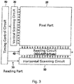
- An electronic apparatus comprises: a solid-state imaging device; and an optical system for forming a subject image on the solid-state imaging device, wherein the solid-state imaging device includes: a pixel part having unit pixel groups arranged therein, the unit pixel groups each including a plurality of pixels at least for visible light that perform photoelectric conversion; and a reading part for reading pixel signals from the pixel part, the plurality of pixels for visible light have a light-receiving sensitivity for infrared light, and in an infrared reading mode, the reading part is capable of adding together signals for infrared light read from the plurality of pixels for visible light.
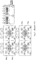
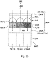
- the pixel PXL12 includes a photodiode PD12 and a transfer transistor TG12-Tr.
- the pixel PXL11 is formed as a Gb pixel
- the pixel PXL12 is formed as a B pixel
- the pixel PXL21 is formed as an R pixel
- the pixel PXL22 is formed as a Gr pixel.
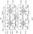
- the third embodiment differs from the first embodiment in the following points.
- the unit pixel groups 200B in the third embodiment are each formed as a unit RGBIR pixel group in which the filter of the pixel PXL22 placed in the arrangement region AR22 is replaced with an infrared-dedicated pixel PXL22B including an infrared (NIR) photoelectric conversion part for receiving infrared light.
- NIR infrared
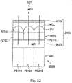
- the unit pixel groups 200C each include an optical filter group 260 including a plurality of optical filters capable of receiving visible light and infrared light having a particular wavelength.
- the optical filter group 260 includes a first optical filter 261 and a second optical filter 262.
- the first optical filter 261 is disposed on the light incidence side of the red filter FLT-R, the green filter FLT-G, and the blue filter FLT-B.
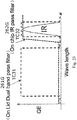
- the fifth embodiment makes it possible to select a desired light wavelength band for imaging with a minimum number of optical filters (IR filters).
- IR filters optical filters
- an IR filter having such a transmittance as shown in Fig. 16 can be used alone for the imaging.
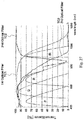
- Fig. 18 is a simplified sectional view showing a schematic configuration of the solid-state imaging device (the CMOS image sensor) according to the sixth embodiment of the present invention.
- Fig. 19 shows transmission characteristics of the color filter array and the optical filters according to the sixth embodiment of the present invention.
- the sixth embodiment is further configured so as to be capable of selecting a pass region (a pass band).
- a pass band a pass band
- the optical filter 261E operates as an IR filter capable of imaging only in the first pass (transmission) region TWB11 ranging over the visible light wavelength band (the visible region) approximately from 380 nm to 700 nm.
- the optical filter 261E operates as an IR filter capable of imaging only in the second pass (transmission) region TWB12 ranging over the infrared light wavelength band (the infrared region) approximately from 850 nm to 1,000 nm.
- imaging is performed by the second optical filter 262 and the third optical filter 263.
- imaging is performed by the first optical filter 261 and the second optical filter 262.
- the tenth embodiment makes it possible not only to obtain the same effect as the fourth embodiment, but also to capture RGB images and NIR images having further reduced cross talk.
- the electronic apparatus 100 includes a CMOS image sensor 110 that can be constituted by the solid-state imaging device 10 according to the embodiments of the present invention. Further, the electronic apparatus 100 includes an optical system (such as a lens) 120 for redirecting the incident light to pixel regions of the CMOS image sensor 110 (to form a subject image). The electronic apparatus 100 includes a signal processing circuit (PRC) 130 for processing output signals of the CMOS image sensor 110.
- CMOS image sensor 110 that can be constituted by the solid-state imaging device 10 according to the embodiments of the present invention.
- the electronic apparatus 100 includes an optical system (such as a lens) 120 for redirecting the incident light to pixel regions of the CMOS image sensor 110 (to form a subject image).
- the electronic apparatus 100 includes a signal processing circuit (PRC) 130 for processing output signals of the CMOS image sensor 110.
- PRC signal processing circuit
Landscapes
- Engineering & Computer Science (AREA)
- Multimedia (AREA)
- Signal Processing (AREA)
- Physics & Mathematics (AREA)
- Spectroscopy & Molecular Physics (AREA)
- Transforming Light Signals Into Electric Signals (AREA)
- Solid State Image Pick-Up Elements (AREA)
Applications Claiming Priority (2)
| Application Number | Priority Date | Filing Date | Title |
|---|---|---|---|
| JP2017230521 | 2017-11-30 | ||
| JP2018194303A JP7280681B2 (ja) | 2017-11-30 | 2018-10-15 | 固体撮像装置、固体撮像装置の駆動方法、および電子機器 |
Publications (4)
| Publication Number | Publication Date |
|---|---|
| EP3493261A2 true EP3493261A2 (fr) | 2019-06-05 |
| EP3493261A3 EP3493261A3 (fr) | 2019-07-24 |
| EP3493261B1 EP3493261B1 (fr) | 2024-02-28 |
| EP3493261C0 EP3493261C0 (fr) | 2024-02-28 |
Family
ID=64572115
Family Applications (1)
| Application Number | Title | Priority Date | Filing Date |
|---|---|---|---|
| EP18209505.9A Active EP3493261B1 (fr) | 2017-11-30 | 2018-11-30 | Dispositif d'imagerie monolithique, procédé d'entraînement de dispositif d'imagerie monolithique et appareil électrique |
Country Status (2)
| Country | Link |
|---|---|
| US (1) | US11153514B2 (fr) |
| EP (1) | EP3493261B1 (fr) |
Cited By (1)
| Publication number | Priority date | Publication date | Assignee | Title |
|---|---|---|---|---|
| EP4142283A1 (fr) * | 2021-08-24 | 2023-03-01 | Aptiv Technologies Limited | Procédé de génération d'image infrarouge |
Families Citing this family (15)
| Publication number | Priority date | Publication date | Assignee | Title |
|---|---|---|---|---|
| JP5999750B2 (ja) * | 2011-08-25 | 2016-09-28 | ソニー株式会社 | 撮像素子、撮像装置及び生体撮像装置 |
| US11621360B2 (en) | 2013-05-22 | 2023-04-04 | W&W Sens Devices, Inc. | Microstructure enhanced absorption photosensitive devices |
| US11121271B2 (en) | 2013-05-22 | 2021-09-14 | W&WSens, Devices, Inc. | Microstructure enhanced absorption photosensitive devices |
| US12087871B2 (en) | 2013-05-22 | 2024-09-10 | W&W Sens Devices, Inc. | Microstructure enhanced absorption photosensitive devices |
| US12243948B2 (en) | 2013-05-22 | 2025-03-04 | W&W Sens Devices, Inc. | Microstructure enhanced absorption photosensitive devices |
| US11791432B2 (en) | 2013-05-22 | 2023-10-17 | W&Wsens Devices, Inc. | Microstructure enhanced absorption photosensitive devices |
| JP2019180048A (ja) | 2018-03-30 | 2019-10-17 | ソニーセミコンダクタソリューションズ株式会社 | 撮像素子および撮像装置 |
| US12094903B2 (en) | 2019-09-24 | 2024-09-17 | W&W Sens Devices, Inc | Microstructure enhanced absorption photosensitive devices |
| EP4059055A4 (fr) * | 2019-09-24 | 2023-12-27 | W&WSENS Devices, Inc. | Dispositifs photosensibles à absorption améliorée par des microstructures |
| JP7314752B2 (ja) * | 2019-09-30 | 2023-07-26 | 株式会社リコー | 光電変換素子、読取装置、画像処理装置および光電変換素子の製造方法 |
| US11694323B2 (en) * | 2020-04-23 | 2023-07-04 | Camx Power Llc | Image-based sensor for measuring rotational position of a rotating shaft |
| KR20220077735A (ko) * | 2020-12-02 | 2022-06-09 | 삼성전자주식회사 | 이미지 센서 및 이미지 센서의 픽셀 어레이 |
| CN112532898B (zh) * | 2020-12-03 | 2022-09-27 | 北京灵汐科技有限公司 | 双模态红外仿生视觉传感器 |
| JP7499695B2 (ja) * | 2020-12-24 | 2024-06-14 | ゼタテクノロジーズ株式会社 | 固体撮像装置、固体撮像装置の信号処理方法、および電子機器 |
| KR20240015496A (ko) * | 2022-07-27 | 2024-02-05 | 삼성전자주식회사 | 이미지 센서 및 이를 포함하는 전자 장치 |
Citations (2)
| Publication number | Priority date | Publication date | Assignee | Title |
|---|---|---|---|---|
| JP2005223681A (ja) | 2004-02-06 | 2005-08-18 | Olympus Corp | 固体撮像装置 |
| JP2017139286A (ja) | 2016-02-02 | 2017-08-10 | ソニー株式会社 | 撮像素子、及び、カメラシステム |
Family Cites Families (55)
| Publication number | Priority date | Publication date | Assignee | Title |
|---|---|---|---|---|
| JP2643326B2 (ja) * | 1988-07-07 | 1997-08-20 | キヤノン株式会社 | 焦点検出装置を有した一眼レフカメラ |
| JP3284659B2 (ja) * | 1993-04-09 | 2002-05-20 | 株式会社フジクラ | 波長多重光通信用光スイッチング装置 |
| US6380539B1 (en) * | 1997-01-30 | 2002-04-30 | Applied Science Fiction, Inc. | Four color trilinear CCD scanning |
| US5924792A (en) * | 1997-02-21 | 1999-07-20 | General Electric Company | Modular dual port central lighting system |
| AU2228799A (en) * | 1998-01-15 | 1999-08-02 | Ciena Corporation | Optical interference filter |
| JP2000304918A (ja) * | 1999-02-19 | 2000-11-02 | Canon Inc | 結像光学系及びそれを用いた原稿読取装置 |
| WO2000062120A1 (fr) * | 1999-04-13 | 2000-10-19 | Matsushita Electric Industrial Co., Ltd. | Afficheur a cristaux liquides |
| JP2002286638A (ja) * | 2001-03-26 | 2002-10-03 | Shimadzu Corp | 同位体ガス測定装置 |
| US20070182844A1 (en) * | 2003-03-09 | 2007-08-09 | Latia Imaging Pty Ltd | Optical system for producing differently focused images |
| KR100970259B1 (ko) * | 2003-08-04 | 2010-07-16 | 삼성전자주식회사 | 액정표시장치 |
| US7411729B2 (en) * | 2004-08-12 | 2008-08-12 | Olympus Corporation | Optical filter, method of manufacturing optical filter, optical system, and imaging apparatus |
| JP4681856B2 (ja) * | 2004-11-24 | 2011-05-11 | アイシン精機株式会社 | カメラの校正方法及びカメラの校正装置 |
| US7456384B2 (en) * | 2004-12-10 | 2008-11-25 | Sony Corporation | Method and apparatus for acquiring physical information, method for manufacturing semiconductor device including array of plurality of unit components for detecting physical quantity distribution, light-receiving device and manufacturing method therefor, and solid-state imaging device and manufacturing method therefor |
| JP4839632B2 (ja) * | 2005-02-25 | 2011-12-21 | ソニー株式会社 | 撮像装置 |
| JP2007311447A (ja) | 2006-05-17 | 2007-11-29 | Sanyo Electric Co Ltd | 光電変換装置 |
| US20080173795A1 (en) * | 2007-01-23 | 2008-07-24 | Hwa-Young Kang | Image sensor |
| TWI370894B (en) * | 2007-02-26 | 2012-08-21 | Corning Inc | Method for measuring distortion |
| KR100863497B1 (ko) * | 2007-06-19 | 2008-10-14 | 마루엘에스아이 주식회사 | 이미지 감지 장치, 이미지 신호 처리 방법, 광 감지 소자, 제어 방법 및 화소 어레이 |
| DE102007054701A1 (de) * | 2007-11-14 | 2009-05-28 | Schott Ag | Farbfilter und Verfahren zu dessen Herstellung |
| JP5793688B2 (ja) * | 2008-07-11 | 2015-10-14 | パナソニックIpマネジメント株式会社 | 固体撮像装置 |
| JP2010093472A (ja) * | 2008-10-07 | 2010-04-22 | Panasonic Corp | 撮像装置および撮像装置用信号処理回路 |
| JP5359465B2 (ja) | 2009-03-31 | 2013-12-04 | ソニー株式会社 | 固体撮像装置、固体撮像装置の信号処理方法および撮像装置 |
| JP5407523B2 (ja) * | 2009-04-24 | 2014-02-05 | ソニー株式会社 | 積分型ad変換装置、固体撮像素子、およびカメラシステム |
| JP5568923B2 (ja) * | 2009-08-25 | 2014-08-13 | 株式会社リコー | 撮像光学系およびカメラ装置および携帯情報端末装置 |
| JP2011075984A (ja) * | 2009-10-01 | 2011-04-14 | Sony Corp | 撮像光学系及び撮像装置 |
| JP5493934B2 (ja) * | 2010-02-03 | 2014-05-14 | ソニー株式会社 | デューティ補正回路、遅延同期ループ回路、カラムa/d変換器、固体撮像素子およびカメラシステム |
| JP5485004B2 (ja) * | 2010-04-23 | 2014-05-07 | パナソニック株式会社 | 撮像装置 |
| JP5521758B2 (ja) * | 2010-05-13 | 2014-06-18 | ソニー株式会社 | 固体撮像素子およびカメラシステム |
| US20120202281A1 (en) * | 2011-02-07 | 2012-08-09 | Pond Biofuels Inc. | Light energy supply for photobioreactor system |
| JP2013055499A (ja) * | 2011-09-02 | 2013-03-21 | Sony Corp | 固体撮像素子およびカメラシステム |
| US10019112B2 (en) * | 2011-10-25 | 2018-07-10 | Semiconductor Components Industries, Llc | Touch panels with dynamic zooming and low profile bezels |
| JP6053505B2 (ja) * | 2012-01-18 | 2016-12-27 | キヤノン株式会社 | 固体撮像装置 |
| US9143704B2 (en) * | 2012-01-20 | 2015-09-22 | Htc Corporation | Image capturing device and method thereof |
| JP5910485B2 (ja) * | 2012-03-16 | 2016-04-27 | 株式会社リコー | 撮像システム |
| EP2876482A4 (fr) * | 2012-07-19 | 2016-04-13 | Nikon Corp | Élément optique, dispositif optique, dispositif de mesure et dispositif de tri |
| JP6161007B2 (ja) * | 2012-09-14 | 2017-07-12 | パナソニックIpマネジメント株式会社 | 固体撮像装置及びカメラモジュール |
| CN107255841B (zh) * | 2012-11-30 | 2020-01-03 | Agc株式会社 | 近红外线截止滤波器 |
| JP6145826B2 (ja) * | 2013-02-07 | 2017-06-14 | パナソニックIpマネジメント株式会社 | 撮像装置及びその駆動方法 |
| EP2871843B1 (fr) * | 2013-11-12 | 2019-05-29 | LG Electronics Inc. -1- | Dispositif numérique et procédé de traitement d'image en trois dimensions de celui-ci |
| JP2015115344A (ja) | 2013-12-09 | 2015-06-22 | 株式会社東芝 | 固体撮像装置 |
| US9739916B2 (en) * | 2014-03-20 | 2017-08-22 | 3M Innovative Properties Company | Circadian rhythm optical film |
| US20150287766A1 (en) * | 2014-04-02 | 2015-10-08 | Tae-Chan Kim | Unit pixel of an image sensor and image sensor including the same |
| JP2015211257A (ja) * | 2014-04-24 | 2015-11-24 | 株式会社東芝 | 固体撮像装置 |
| US10002893B2 (en) | 2014-05-19 | 2018-06-19 | Samsung Electronics Co., Ltd. | Image sensor including hybrid pixel structure |
| WO2015186225A1 (fr) * | 2014-06-05 | 2015-12-10 | 株式会社ニコン | Dispositif de projection du type à balayage, procédé de projection, et système d'assistance chirurgicale |
| JP2015233185A (ja) * | 2014-06-09 | 2015-12-24 | 株式会社東芝 | 固体撮像装置 |
| US10594996B2 (en) * | 2014-09-24 | 2020-03-17 | Sony Semiconductor Solutions Corporation | Image processing apparatus, image pickup device, image pickup apparatus, and image processing method |
| US20160161332A1 (en) * | 2014-12-09 | 2016-06-09 | Stmicroelectronics (Research & Development) Limited | Image sensor using pixels with combined rgb and ir sensing |
| JP6535461B2 (ja) * | 2014-12-16 | 2019-06-26 | 株式会社トプコン | 材料分析センサ及び材料分析装置 |
| US10627646B2 (en) * | 2015-05-20 | 2020-04-21 | Canon Kabushiki Kaisha | Image pickup optical system and image pickup apparatus |
| US20170034456A1 (en) | 2015-07-31 | 2017-02-02 | Dual Aperture International Co., Ltd. | Sensor assembly with selective infrared filter array |
| US10389922B2 (en) * | 2015-08-15 | 2019-08-20 | Nikon Corporation | Multi-wavelength detector |
| US10132971B2 (en) * | 2016-03-04 | 2018-11-20 | Magna Electronics Inc. | Vehicle camera with multiple spectral filters |
| JP6753169B2 (ja) * | 2016-06-28 | 2020-09-09 | セイコーエプソン株式会社 | 画像読取装置及び半導体装置 |
| US10444415B2 (en) * | 2017-02-14 | 2019-10-15 | Cista System Corp. | Multispectral sensing system and method |
-
2018
- 2018-11-28 US US16/203,136 patent/US11153514B2/en active Active
- 2018-11-30 EP EP18209505.9A patent/EP3493261B1/fr active Active
Patent Citations (2)
| Publication number | Priority date | Publication date | Assignee | Title |
|---|---|---|---|---|
| JP2005223681A (ja) | 2004-02-06 | 2005-08-18 | Olympus Corp | 固体撮像装置 |
| JP2017139286A (ja) | 2016-02-02 | 2017-08-10 | ソニー株式会社 | 撮像素子、及び、カメラシステム |
Cited By (2)
| Publication number | Priority date | Publication date | Assignee | Title |
|---|---|---|---|---|
| EP4142283A1 (fr) * | 2021-08-24 | 2023-03-01 | Aptiv Technologies Limited | Procédé de génération d'image infrarouge |
| US12075170B2 (en) | 2021-08-24 | 2024-08-27 | Aptiv Technologies AG | Method of generating infrared image |
Also Published As
| Publication number | Publication date |
|---|---|
| US11153514B2 (en) | 2021-10-19 |
| US20190166317A1 (en) | 2019-05-30 |
| EP3493261B1 (fr) | 2024-02-28 |
| EP3493261A3 (fr) | 2019-07-24 |
| EP3493261C0 (fr) | 2024-02-28 |
Similar Documents
| Publication | Publication Date | Title |
|---|---|---|
| EP3493261B1 (fr) | Dispositif d'imagerie monolithique, procédé d'entraînement de dispositif d'imagerie monolithique et appareil électrique | |
| JP7280681B2 (ja) | 固体撮像装置、固体撮像装置の駆動方法、および電子機器 | |
| JP5082528B2 (ja) | 固体撮像装置及び撮像装置 | |
| US20220415949A1 (en) | Solid-state imaging apparatus, method for manufacturing the same, and electronic device | |
| US20140184808A1 (en) | Photoelectric Conversion Device and Imaging Apparatus Having the Photoelectric Conversion Device | |
| US8878969B2 (en) | Imaging systems with color filter barriers | |
| WO2017126326A1 (fr) | Dispositif de capture d'image monolithique et son procédé de commande, et instrument électronique | |
| JP7499695B2 (ja) | 固体撮像装置、固体撮像装置の信号処理方法、および電子機器 | |
| JP2010206678A (ja) | 固体撮像装置、撮像モジュール、及び撮像システム | |
| WO2021159944A1 (fr) | Capteur d'image, ensemble caméra et terminal mobile | |
| JP6970595B2 (ja) | 固体撮像装置、固体撮像装置の製造方法、および電子機器 | |
| JP2020027937A (ja) | 固体撮像装置、固体撮像装置の製造方法、および電子機器 | |
| CN107251544B (zh) | 固态成像装置、驱动方法和电子设备 | |
| US11784203B2 (en) | Solid-state imaging device, method for manufacturing solid-state imaging device and electronic apparatus having a multi-pixel having a back side separating part | |
| US20240397227A1 (en) | Solid-state imaging device, method for manufacturing solid-state imaging device, and electronic apparatus | |
| CN103685997A (zh) | 固体拍摄装置、拍摄方法及相机模块 | |
| JP7404447B1 (ja) | 固体撮像装置、固体撮像装置の製造方法、および電子機器 | |
| WO2021046690A1 (fr) | Capteur d'images, module de caméra, terminal mobile et procédé de capture d'images | |
| US20240089619A1 (en) | Light detection device and electronic apparatus | |
| JP7487151B2 (ja) | 固体撮像装置、固体撮像装置の製造方法、および電子機器 | |
| JP7525586B2 (ja) | 固体撮像装置、固体撮像装置の製造方法、および電子機器 | |
| KR20150016872A (ko) | 고체 촬상 장치 및 고체 촬상 장치의 제조 방법 |
Legal Events
| Date | Code | Title | Description |
|---|---|---|---|
| PUAI | Public reference made under article 153(3) epc to a published international application that has entered the european phase |
Free format text: ORIGINAL CODE: 0009012 |
|
| STAA | Information on the status of an ep patent application or granted ep patent |
Free format text: STATUS: THE APPLICATION HAS BEEN PUBLISHED |
|
| AK | Designated contracting states |
Kind code of ref document: A2 Designated state(s): AL AT BE BG CH CY CZ DE DK EE ES FI FR GB GR HR HU IE IS IT LI LT LU LV MC MK MT NL NO PL PT RO RS SE SI SK SM TR |
|
| AX | Request for extension of the european patent |
Extension state: BA ME |
|
| PUAL | Search report despatched |
Free format text: ORIGINAL CODE: 0009013 |
|
| AK | Designated contracting states |
Kind code of ref document: A3 Designated state(s): AL AT BE BG CH CY CZ DE DK EE ES FI FR GB GR HR HU IE IS IT LI LT LU LV MC MK MT NL NO PL PT RO RS SE SI SK SM TR |
|
| AX | Request for extension of the european patent |
Extension state: BA ME |
|
| RIC1 | Information provided on ipc code assigned before grant |
Ipc: H04N 9/04 20060101ALI20190618BHEP Ipc: H01L 27/146 20060101AFI20190618BHEP Ipc: H04N 5/33 20060101ALI20190618BHEP |
|
| STAA | Information on the status of an ep patent application or granted ep patent |
Free format text: STATUS: REQUEST FOR EXAMINATION WAS MADE |
|
| 17P | Request for examination filed |
Effective date: 20200123 |
|
| RBV | Designated contracting states (corrected) |
Designated state(s): AL AT BE BG CH CY CZ DE DK EE ES FI FR GB GR HR HU IE IS IT LI LT LU LV MC MK MT NL NO PL PT RO RS SE SI SK SM TR |
|
| STAA | Information on the status of an ep patent application or granted ep patent |
Free format text: STATUS: EXAMINATION IS IN PROGRESS |
|
| RAP1 | Party data changed (applicant data changed or rights of an application transferred) |
Owner name: BRILLNICS SINGAPORE PTE. LTD. |
|
| 17Q | First examination report despatched |
Effective date: 20210611 |
|
| RIC1 | Information provided on ipc code assigned before grant |
Ipc: H04N 25/778 20230101ALI20230728BHEP Ipc: H04N 25/131 20230101ALI20230728BHEP Ipc: H04N 23/11 20230101ALI20230728BHEP Ipc: H04N 5/33 20060101ALI20230728BHEP Ipc: H01L 27/146 20060101AFI20230728BHEP |
|
| GRAP | Despatch of communication of intention to grant a patent |
Free format text: ORIGINAL CODE: EPIDOSNIGR1 |
|
| STAA | Information on the status of an ep patent application or granted ep patent |
Free format text: STATUS: GRANT OF PATENT IS INTENDED |
|
| INTG | Intention to grant announced |
Effective date: 20230920 |
|
| GRAS | Grant fee paid |
Free format text: ORIGINAL CODE: EPIDOSNIGR3 |
|
| GRAA | (expected) grant |
Free format text: ORIGINAL CODE: 0009210 |
|
| STAA | Information on the status of an ep patent application or granted ep patent |
Free format text: STATUS: THE PATENT HAS BEEN GRANTED |
|
| AK | Designated contracting states |
Kind code of ref document: B1 Designated state(s): AL AT BE BG CH CY CZ DE DK EE ES FI FR GB GR HR HU IE IS IT LI LT LU LV MC MK MT NL NO PL PT RO RS SE SI SK SM TR |
|
| REG | Reference to a national code |
Ref country code: GB Ref legal event code: FG4D |
|
| REG | Reference to a national code |
Ref country code: CH Ref legal event code: EP |
|
| REG | Reference to a national code |
Ref country code: DE Ref legal event code: R096 Ref document number: 602018065800 Country of ref document: DE |
|
| REG | Reference to a national code |
Ref country code: IE Ref legal event code: FG4D |
|
| U01 | Request for unitary effect filed |
Effective date: 20240328 |
|
| U07 | Unitary effect registered |
Designated state(s): AT BE BG DE DK EE FI FR IT LT LU LV MT NL PT SE SI Effective date: 20240410 |
|
| PG25 | Lapsed in a contracting state [announced via postgrant information from national office to epo] |
Ref country code: IS Free format text: LAPSE BECAUSE OF FAILURE TO SUBMIT A TRANSLATION OF THE DESCRIPTION OR TO PAY THE FEE WITHIN THE PRESCRIBED TIME-LIMIT Effective date: 20240628 |
|
| PG25 | Lapsed in a contracting state [announced via postgrant information from national office to epo] |
Ref country code: GR Free format text: LAPSE BECAUSE OF FAILURE TO SUBMIT A TRANSLATION OF THE DESCRIPTION OR TO PAY THE FEE WITHIN THE PRESCRIBED TIME-LIMIT Effective date: 20240529 |
|
| PG25 | Lapsed in a contracting state [announced via postgrant information from national office to epo] |
Ref country code: RS Free format text: LAPSE BECAUSE OF FAILURE TO SUBMIT A TRANSLATION OF THE DESCRIPTION OR TO PAY THE FEE WITHIN THE PRESCRIBED TIME-LIMIT Effective date: 20240528 Ref country code: HR Free format text: LAPSE BECAUSE OF FAILURE TO SUBMIT A TRANSLATION OF THE DESCRIPTION OR TO PAY THE FEE WITHIN THE PRESCRIBED TIME-LIMIT Effective date: 20240228 |
|
| PG25 | Lapsed in a contracting state [announced via postgrant information from national office to epo] |
Ref country code: ES Free format text: LAPSE BECAUSE OF FAILURE TO SUBMIT A TRANSLATION OF THE DESCRIPTION OR TO PAY THE FEE WITHIN THE PRESCRIBED TIME-LIMIT Effective date: 20240228 |
|
| PG25 | Lapsed in a contracting state [announced via postgrant information from national office to epo] |
Ref country code: RS Free format text: LAPSE BECAUSE OF FAILURE TO SUBMIT A TRANSLATION OF THE DESCRIPTION OR TO PAY THE FEE WITHIN THE PRESCRIBED TIME-LIMIT Effective date: 20240528 Ref country code: NO Free format text: LAPSE BECAUSE OF FAILURE TO SUBMIT A TRANSLATION OF THE DESCRIPTION OR TO PAY THE FEE WITHIN THE PRESCRIBED TIME-LIMIT Effective date: 20240528 Ref country code: IS Free format text: LAPSE BECAUSE OF FAILURE TO SUBMIT A TRANSLATION OF THE DESCRIPTION OR TO PAY THE FEE WITHIN THE PRESCRIBED TIME-LIMIT Effective date: 20240628 Ref country code: HR Free format text: LAPSE BECAUSE OF FAILURE TO SUBMIT A TRANSLATION OF THE DESCRIPTION OR TO PAY THE FEE WITHIN THE PRESCRIBED TIME-LIMIT Effective date: 20240228 Ref country code: GR Free format text: LAPSE BECAUSE OF FAILURE TO SUBMIT A TRANSLATION OF THE DESCRIPTION OR TO PAY THE FEE WITHIN THE PRESCRIBED TIME-LIMIT Effective date: 20240529 Ref country code: ES Free format text: LAPSE BECAUSE OF FAILURE TO SUBMIT A TRANSLATION OF THE DESCRIPTION OR TO PAY THE FEE WITHIN THE PRESCRIBED TIME-LIMIT Effective date: 20240228 |
|
| PG25 | Lapsed in a contracting state [announced via postgrant information from national office to epo] |
Ref country code: PL Free format text: LAPSE BECAUSE OF FAILURE TO SUBMIT A TRANSLATION OF THE DESCRIPTION OR TO PAY THE FEE WITHIN THE PRESCRIBED TIME-LIMIT Effective date: 20240228 |
|
| PG25 | Lapsed in a contracting state [announced via postgrant information from national office to epo] |
Ref country code: PL Free format text: LAPSE BECAUSE OF FAILURE TO SUBMIT A TRANSLATION OF THE DESCRIPTION OR TO PAY THE FEE WITHIN THE PRESCRIBED TIME-LIMIT Effective date: 20240228 |
|
| PG25 | Lapsed in a contracting state [announced via postgrant information from national office to epo] |
Ref country code: SM Free format text: LAPSE BECAUSE OF FAILURE TO SUBMIT A TRANSLATION OF THE DESCRIPTION OR TO PAY THE FEE WITHIN THE PRESCRIBED TIME-LIMIT Effective date: 20240228 |
|
| PG25 | Lapsed in a contracting state [announced via postgrant information from national office to epo] |
Ref country code: CZ Free format text: LAPSE BECAUSE OF FAILURE TO SUBMIT A TRANSLATION OF THE DESCRIPTION OR TO PAY THE FEE WITHIN THE PRESCRIBED TIME-LIMIT Effective date: 20240228 |
|
| PG25 | Lapsed in a contracting state [announced via postgrant information from national office to epo] |
Ref country code: SK Free format text: LAPSE BECAUSE OF FAILURE TO SUBMIT A TRANSLATION OF THE DESCRIPTION OR TO PAY THE FEE WITHIN THE PRESCRIBED TIME-LIMIT Effective date: 20240228 |
|
| PG25 | Lapsed in a contracting state [announced via postgrant information from national office to epo] |
Ref country code: SM Free format text: LAPSE BECAUSE OF FAILURE TO SUBMIT A TRANSLATION OF THE DESCRIPTION OR TO PAY THE FEE WITHIN THE PRESCRIBED TIME-LIMIT Effective date: 20240228 Ref country code: SK Free format text: LAPSE BECAUSE OF FAILURE TO SUBMIT A TRANSLATION OF THE DESCRIPTION OR TO PAY THE FEE WITHIN THE PRESCRIBED TIME-LIMIT Effective date: 20240228 Ref country code: RO Free format text: LAPSE BECAUSE OF FAILURE TO SUBMIT A TRANSLATION OF THE DESCRIPTION OR TO PAY THE FEE WITHIN THE PRESCRIBED TIME-LIMIT Effective date: 20240228 Ref country code: CZ Free format text: LAPSE BECAUSE OF FAILURE TO SUBMIT A TRANSLATION OF THE DESCRIPTION OR TO PAY THE FEE WITHIN THE PRESCRIBED TIME-LIMIT Effective date: 20240228 |
|
| U20 | Renewal fee for the european patent with unitary effect paid |
Year of fee payment: 7 Effective date: 20241007 |
|
| REG | Reference to a national code |
Ref country code: DE Ref legal event code: R097 Ref document number: 602018065800 Country of ref document: DE |
|
| PLBE | No opposition filed within time limit |
Free format text: ORIGINAL CODE: 0009261 |
|
| STAA | Information on the status of an ep patent application or granted ep patent |
Free format text: STATUS: NO OPPOSITION FILED WITHIN TIME LIMIT |
|
| 26N | No opposition filed |
Effective date: 20241129 |
|
| REG | Reference to a national code |
Ref country code: CH Ref legal event code: PL |
|
| PG25 | Lapsed in a contracting state [announced via postgrant information from national office to epo] |
Ref country code: MC Free format text: LAPSE BECAUSE OF FAILURE TO SUBMIT A TRANSLATION OF THE DESCRIPTION OR TO PAY THE FEE WITHIN THE PRESCRIBED TIME-LIMIT Effective date: 20240228 |
|
| REG | Reference to a national code |
Ref country code: CH Ref legal event code: PL |
|
| PG25 | Lapsed in a contracting state [announced via postgrant information from national office to epo] |
Ref country code: CH Free format text: LAPSE BECAUSE OF NON-PAYMENT OF DUE FEES Effective date: 20241130 |
|
| PG25 | Lapsed in a contracting state [announced via postgrant information from national office to epo] |
Ref country code: IE Free format text: LAPSE BECAUSE OF NON-PAYMENT OF DUE FEES Effective date: 20241130 |
|
| U20 | Renewal fee for the european patent with unitary effect paid |
Year of fee payment: 8 Effective date: 20251008 |
|
| PGFP | Annual fee paid to national office [announced via postgrant information from national office to epo] |
Ref country code: GB Payment date: 20251001 Year of fee payment: 8 |
|
| PG25 | Lapsed in a contracting state [announced via postgrant information from national office to epo] |
Ref country code: CY Free format text: LAPSE BECAUSE OF FAILURE TO SUBMIT A TRANSLATION OF THE DESCRIPTION OR TO PAY THE FEE WITHIN THE PRESCRIBED TIME-LIMIT; INVALID AB INITIO Effective date: 20181130 |