EP3495861B1 - Photonen-chip mit rückfaltung des lichtwegs und integrierter bündelungsstruktur - Google Patents
Photonen-chip mit rückfaltung des lichtwegs und integrierter bündelungsstruktur Download PDFInfo
- Publication number
- EP3495861B1 EP3495861B1 EP18210428.1A EP18210428A EP3495861B1 EP 3495861 B1 EP3495861 B1 EP 3495861B1 EP 18210428 A EP18210428 A EP 18210428A EP 3495861 B1 EP3495861 B1 EP 3495861B1
- Authority
- EP
- European Patent Office
- Prior art keywords
- photonic chip
- light
- layer
- light guide
- collimation structure
- Prior art date
- Legal status (The legal status is an assumption and is not a legal conclusion. Google has not performed a legal analysis and makes no representation as to the accuracy of the status listed.)
- Active
Links
Images


Classifications
-
- G—PHYSICS
- G02—OPTICS
- G02B—OPTICAL ELEMENTS, SYSTEMS OR APPARATUS
- G02B6/00—Light guides; Structural details of arrangements comprising light guides and other optical elements, e.g. couplings
- G02B6/10—Light guides; Structural details of arrangements comprising light guides and other optical elements, e.g. couplings of the optical waveguide type
- G02B6/12—Light guides; Structural details of arrangements comprising light guides and other optical elements, e.g. couplings of the optical waveguide type of the integrated circuit kind
- G02B6/122—Basic optical elements, e.g. light-guiding paths
- G02B6/124—Geodesic lenses or integrated gratings
-
- G—PHYSICS
- G02—OPTICS
- G02B—OPTICAL ELEMENTS, SYSTEMS OR APPARATUS
- G02B6/00—Light guides; Structural details of arrangements comprising light guides and other optical elements, e.g. couplings
- G02B6/10—Light guides; Structural details of arrangements comprising light guides and other optical elements, e.g. couplings of the optical waveguide type
- G02B6/12—Light guides; Structural details of arrangements comprising light guides and other optical elements, e.g. couplings of the optical waveguide type of the integrated circuit kind
- G02B6/12004—Combinations of two or more optical elements
-
- G—PHYSICS
- G02—OPTICS
- G02B—OPTICAL ELEMENTS, SYSTEMS OR APPARATUS
- G02B6/00—Light guides; Structural details of arrangements comprising light guides and other optical elements, e.g. couplings
- G02B6/10—Light guides; Structural details of arrangements comprising light guides and other optical elements, e.g. couplings of the optical waveguide type
- G02B6/12—Light guides; Structural details of arrangements comprising light guides and other optical elements, e.g. couplings of the optical waveguide type of the integrated circuit kind
- G02B6/13—Integrated optical circuits characterised by the manufacturing method
-
- G—PHYSICS
- G02—OPTICS
- G02B—OPTICAL ELEMENTS, SYSTEMS OR APPARATUS
- G02B6/00—Light guides; Structural details of arrangements comprising light guides and other optical elements, e.g. couplings
- G02B6/10—Light guides; Structural details of arrangements comprising light guides and other optical elements, e.g. couplings of the optical waveguide type
- G02B6/12—Light guides; Structural details of arrangements comprising light guides and other optical elements, e.g. couplings of the optical waveguide type of the integrated circuit kind
- G02B6/13—Integrated optical circuits characterised by the manufacturing method
- G02B6/136—Integrated optical circuits characterised by the manufacturing method by etching
-
- G—PHYSICS
- G02—OPTICS
- G02B—OPTICAL ELEMENTS, SYSTEMS OR APPARATUS
- G02B6/00—Light guides; Structural details of arrangements comprising light guides and other optical elements, e.g. couplings
- G02B6/24—Coupling light guides
- G02B6/26—Optical coupling means
- G02B6/30—Optical coupling means for use between fibre and thin-film device
-
- G—PHYSICS
- G02—OPTICS
- G02B—OPTICAL ELEMENTS, SYSTEMS OR APPARATUS
- G02B6/00—Light guides; Structural details of arrangements comprising light guides and other optical elements, e.g. couplings
- G02B6/24—Coupling light guides
- G02B6/42—Coupling light guides with opto-electronic elements
- G02B6/4201—Packages, e.g. shape, construction, internal or external details
- G02B6/4204—Packages, e.g. shape, construction, internal or external details the coupling comprising intermediate optical elements, e.g. lenses, holograms
- G02B6/4206—Optical features
-
- H—ELECTRICITY
- H01—ELECTRIC ELEMENTS
- H01S—DEVICES USING THE PROCESS OF LIGHT AMPLIFICATION BY STIMULATED EMISSION OF RADIATION [LASER] TO AMPLIFY OR GENERATE LIGHT; DEVICES USING STIMULATED EMISSION OF ELECTROMAGNETIC RADIATION IN WAVE RANGES OTHER THAN OPTICAL
- H01S5/00—Semiconductor lasers
- H01S5/10—Construction or shape of the optical resonator, e.g. extended or external cavity, coupled cavities, bent-guide, varying width, thickness or composition of the active region
- H01S5/18—Surface-emitting [SE] lasers, e.g. having both horizontal and vertical cavities
- H01S5/185—Surface-emitting [SE] lasers, e.g. having both horizontal and vertical cavities having only horizontal cavities, e.g. horizontal cavity surface-emitting lasers [HCSEL]
-
- G—PHYSICS
- G02—OPTICS
- G02B—OPTICAL ELEMENTS, SYSTEMS OR APPARATUS
- G02B6/00—Light guides; Structural details of arrangements comprising light guides and other optical elements, e.g. couplings
- G02B6/10—Light guides; Structural details of arrangements comprising light guides and other optical elements, e.g. couplings of the optical waveguide type
- G02B6/12—Light guides; Structural details of arrangements comprising light guides and other optical elements, e.g. couplings of the optical waveguide type of the integrated circuit kind
- G02B2006/12083—Constructional arrangements
- G02B2006/12104—Mirror; Reflectors or the like
-
- G—PHYSICS
- G02—OPTICS
- G02B—OPTICAL ELEMENTS, SYSTEMS OR APPARATUS
- G02B6/00—Light guides; Structural details of arrangements comprising light guides and other optical elements, e.g. couplings
- G02B6/10—Light guides; Structural details of arrangements comprising light guides and other optical elements, e.g. couplings of the optical waveguide type
- G02B6/12—Light guides; Structural details of arrangements comprising light guides and other optical elements, e.g. couplings of the optical waveguide type of the integrated circuit kind
- G02B2006/12083—Constructional arrangements
- G02B2006/12107—Grating
-
- G—PHYSICS
- G02—OPTICS
- G02B—OPTICAL ELEMENTS, SYSTEMS OR APPARATUS
- G02B6/00—Light guides; Structural details of arrangements comprising light guides and other optical elements, e.g. couplings
- G02B6/10—Light guides; Structural details of arrangements comprising light guides and other optical elements, e.g. couplings of the optical waveguide type
- G02B6/12—Light guides; Structural details of arrangements comprising light guides and other optical elements, e.g. couplings of the optical waveguide type of the integrated circuit kind
- G02B2006/12133—Functions
- G02B2006/12147—Coupler
-
- H—ELECTRICITY
- H01—ELECTRIC ELEMENTS
- H01S—DEVICES USING THE PROCESS OF LIGHT AMPLIFICATION BY STIMULATED EMISSION OF RADIATION [LASER] TO AMPLIFY OR GENERATE LIGHT; DEVICES USING STIMULATED EMISSION OF ELECTROMAGNETIC RADIATION IN WAVE RANGES OTHER THAN OPTICAL
- H01S5/00—Semiconductor lasers
- H01S5/005—Optical components external to the laser cavity, specially adapted therefor, e.g. for homogenisation or merging of the beams or for manipulating laser pulses, e.g. pulse shaping
- H01S5/0071—Optical components external to the laser cavity, specially adapted therefor, e.g. for homogenisation or merging of the beams or for manipulating laser pulses, e.g. pulse shaping for beam steering, e.g. using a mirror outside the cavity to change the beam direction
-
- H—ELECTRICITY
- H01—ELECTRIC ELEMENTS
- H01S—DEVICES USING THE PROCESS OF LIGHT AMPLIFICATION BY STIMULATED EMISSION OF RADIATION [LASER] TO AMPLIFY OR GENERATE LIGHT; DEVICES USING STIMULATED EMISSION OF ELECTROMAGNETIC RADIATION IN WAVE RANGES OTHER THAN OPTICAL
- H01S5/00—Semiconductor lasers
- H01S5/10—Construction or shape of the optical resonator, e.g. extended or external cavity, coupled cavities, bent-guide, varying width, thickness or composition of the active region
- H01S5/18—Surface-emitting [SE] lasers, e.g. having both horizontal and vertical cavities
- H01S5/185—Surface-emitting [SE] lasers, e.g. having both horizontal and vertical cavities having only horizontal cavities, e.g. horizontal cavity surface-emitting lasers [HCSEL]
- H01S5/187—Surface-emitting [SE] lasers, e.g. having both horizontal and vertical cavities having only horizontal cavities, e.g. horizontal cavity surface-emitting lasers [HCSEL] using Bragg reflection
Definitions
- the field of the invention is that of integrated photonics on chip or integrated circuit.
- the invention relates to a photonic chip which has input(s)/output(s), to/from the chip, of light beams having an enlarged mode size for coupling with an external device, for example with another photonic chip , an optical fiber or an assembly of optical fibers, or for reception/emission of a freely propagating light beam.
- Photonic Integrated Circuit comprises several components interconnected with one another by light waveguides. Since the photonic circuit generally has to communicate with the outside world, it is necessary to be able to inject/extract light into/from the circuit in the form of an unguided light beam.
- a surface coupling network makes it possible, on the one hand, to adapt the size of the optical mode propagating in the waveguides of the photonic chip to the size of the optical mode propagating in the standard single-mode fibers, i.e. ie a diameter of 9.2 ⁇ m, and, on the other hand, to switch from guided propagation in the plane of the photonic chip to propagation in free space quasi-vertical to the plane of the chip. This is obtained by etching a network in the layer comprising the waveguides.
- a such a component is for example described in: "Apodized Waveguide Grating Couplers for Efficient Coupling to Optical Fibers", IEEE PHOTONICS TECHNOLOGY LETTERS, VOL. 22, NO. 15, AUGUST 1, 2010, by Xia Chen and alter .
- this component thus makes it possible to couple the light from a waveguide in the plane of the photonic chip to a cleaved single-mode fiber making an angle with the vertical, commonly around 8°.
- the losses of this component are 1 to 4 dB optical when the geometrical alignment between the surface coupling network and the monomode fiber is optimal.
- the grating-fiber alignment tolerance characterized as the radial misalignment with respect to the optimal alignment which generates 1 dB of additional losses, is approximately 2 ⁇ m.
- the alignment tolerance between the chip+first lens assembly and the second lens+fiber assembly is then increased to +/- 10 to 20 ⁇ m.
- this system makes it possible to relax the alignment constraints between the chip + first lens assembly and the fiber + second lens assembly, it has the disadvantage of transferring the alignment constraints between the first lens and the photonic chip to accuracy less than 1 ⁇ m. Furthermore, if the fact of extracting a collimated beam of enlarged size makes it possible to increase the alignment tolerance of the chip with an opto-mechanical interface part opposite the face of the chip, the angular reception tolerance is reduced.
- the profile of this surface is thus qualified as analog.
- the manufacture of such an analog profile by etching uses a technique of lithography by resin flow or by so-called “Gray tone” lithography which has the drawback of being difficult to calibrate to obtain the desired analog shapes.
- anti-reflective coatings are particularly fragile in a hot/humid environment (85°C/85% humidity), which requires the use of airtight packaging.
- the lens is positioned on the front face of the chip, opposite a surface coupling network which emits in the direction of the front face.
- the lens thus has a focal length potentially equal to the distance between the lens and the surface coupling network.
- the lens must be made in the encapsulation layer through which the beam passes on the coupler/lens path, which is usually only a few microns.
- a thickness of more than 400 ⁇ m of SiO 2 would be necessary to pass from a mode size at the output of the coupler of 9.2 ⁇ m to a mode size at the output of the lens of 55 ⁇ m.
- the manufacture of the lens on the front face has the disadvantage of requiring additional manufacturing steps after manufacture of the photonic chip, above the photonic chip while the top of the photonic chip generally contains lines of metal interconnection of photonic components with external electronic circuits.
- the lens is positioned on the rear face, opposite a waveguide ending in an inclined facet covered with a mirror (called “faceted waveguide” thereafter), and directing the beam towards the rear face of the chip.
- the lens is positioned in the layer comprising the waveguides. No practical implementation of this variant is nevertheless described, and in particular no implementation making it possible to widen the mode size of the beam at the output of a vertical coupler.
- the lenses used in the patent US 8,515,217 B2 are analogue Fresnel lenses.
- a Fresnel lens replaces the curved surface of a conventional lens with a series of concentric rings of different prismatic sections from ring to ring.
- the thickness of a Fresnel lens is therefore reduced compared to a conventional lens, but its manufacture remains difficult. It requires analog structuring in sawtooth, making it possible to define crests of variable inclinations, generally produced by the “Gray tone” lithography technique.
- Such a Fresnel lens also remains sensitive to Fresnel reflections.
- such a lens is sensitive to the polarization of light due to the rings.
- the electric field of the optical wave can take any orientation in the plan of the chip and the indices seen by the wave, on the scale of the wavelength, differ according to the orientation of the field electric.
- US 2002/003824 A1 discloses a photonic chip equipped with a laser which emits light in a guiding layer in the direction of a faceted waveguide which will reflect the light towards the rear face of the chip.
- the rear side has a reflective structure that reflects light back to the front side of the chip.
- a lens is formed on the front face of the chip.
- the object of the invention is to provide a photonic chip with means capable of collimating and widening an optical beam at the output of the photonic chip (and conversely to focus and adapt an optical beam at the input of the photonic chip to a vertical coupling structure of the photonic chip). And the invention seeks to simplify the manufacture of such a chip, in particular to overcome the manufacturing disadvantages mentioned above (analogue profile, anti-reflection treatment).
- the invention also aims to solve the problem of sensitivity of the angular alignment between the chip from which a collimated beam of enlarged size is extracted and the opto-mechanical interface part facing the face of the chip.
- the invention proposes for this purpose a photonic chip comprising a light guiding layer supported by a substrate and covered by an encapsulation layer, the photonic chip having a front face on the side of the encapsulation layer and a rear face on the side of the substrate.
- the light guiding layer includes a light guiding structure comprising a waveguide and optically coupled to a vertical coupler configured to receive light from the waveguide and form a beam of light directed toward the one of the front and back sides.
- the photonic chip further includes a collimating structure formed at least in part in the light guide layer, as well as a arrangement of one or more reflective structures each on one of the front and rear faces, said arrangement being made in such a way as to ensure the propagation of light between the vertical coupler and the collimating structure along an optical path having at least one folding .
- the collimating structure integrated at least in part in the light guiding layer can present a digital profile which can be obtained by means of standard manufacturing methods used for the structuring of the components of the light guiding layer. .
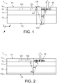
- the invention relates to a photonic chip 1 which comprises a light-guiding layer 12 supported by a substrate 10 and covered by an encapsulation layer 13.
- the light-guiding layer has a thickness generally comprised between 100 nm and 3 ⁇ m.
- the light-guiding layer can be made of silicon, of InP, of GaAs, of Ge, or of one or more type III-V or IV semiconductor materials.
- a buried oxide layer 11 may be interposed between the light guiding layer 12 and the substrate 10.
- the substrate may be made of silicon, indium phosphide or gallium arsenide.
- the encapsulation layer 13 can be a layer of dielectric material, for example silicon oxide, silicon nitride, polymer based on BCB (benzocyclobutene).
- the photonic chip 1 has a front face F1 on the side of the encapsulation layer 13 and a rear face F2 on the side of the substrate 10.
- the light guide layer comprises a light guide structure 121 coupled to a vertical coupler 122 configured to receive light from the light guide structure and form therefrom a light beam directed to one of the front and rear faces.
- vertical coupler we mean a coupler making it possible to pass from guided propagation in the plane of the chip (plane (xy) on the figure 1 ) to vertical or quasi-vertical propagation, typically forming an angle less than 90°, and preferably between 0 and 45°, with the normal to the front and rear faces of the chip (this normal extending in the direction z on the figure 1 ), for example an angle ⁇ 1 of 8° in an encapsulation layer 13 of SiO 2 .
- the vertical coupler can be a grating coupler.
- the vertical coupler can also be a faceted waveguide type coupler.
- the light guiding structure 121 comprises the various photonic components, passive or active, up to the vertical coupler 122. It notably comprises a waveguide, here represented with the vertical coupler 122 according to a longitudinal section, the light propagating on the figure 1 along the x direction.
- the encapsulation layer 13 generally comprises electrical interconnection metal levels of the photonic chip. This layer is thus made up of dielectric materials and etched lines of metal. An electronic chip intended to control or read the active photonic components of the photonic chip (modulators, photo-detectors) is generally transferred to the front face of the photonic chip.
- the length of the optical path between the vertical coupler 122 and the rear face F2 of the chip can be approximated as being the thickness of the substrate 10.
- the optical index at the wavelength 1.31 ⁇ m is approximately 3.5, and the necessary thickness of material to obtain a collimated widened beam with a diameter of 80 ⁇ m is of the order of 1550 ⁇ m.
- the thickness of the substrate is typically 775 ⁇ m+/-25 ⁇ m for a 300mm diameter silicon substrate, 625 ⁇ m+/-25 ⁇ m for a 75mm diameter InP substrate, and 450 ⁇ m for a 75mm diameter GaAs substrate.
- the thickness of the substrate 10 is therefore generally insufficient to allow the diameter of the beam to be widened in a satisfactory manner.
- the invention proposes a photonic chip which is provided with an arrangement of one or more reflective structures 151, 152 each on one of the front and rear faces. This arrangement is made in such a way as to ensure the propagation of light between the vertical coupler 122 and a light collimation structure 14 formed at least in part in the light guiding layer 12, this propagation taking place along a path optic having at least one folding in the substrate.
- this arrangement comprises a reflective structure 152 on the rear face.
- the optical path comprises at least one double passage through the substrate 10.
- a reflective structure of said arrangement is a metallic layer deposited on one of the front and rear faces, for example a layer of gold, silver or aluminum.
- a reflective structure of said arrangement is a distributed Bragg reflector (DBR for “Distributed Bragg Reflector”) formed from a stack of layers deposited on one of the front and rear faces.
- DBR distributed Bragg reflector
- a reflective structure is formed locally on one of the front and rear faces of the photonic chip.
- a reflective structure can be formed on the whole of one of the front and rear faces of the photonic chip, for example on the whole of the rear face as shown in the embodiment of the figure 2 .
- the following description more particularly takes the example of the transmission of light from the guide structure of the photonic chip towards the external device (light extraction), the collimation structure forming a light exit port.
- the principles presented are however perfectly identical for a transmission of light from the external device in the direction of the guiding structure of the photonic chip (injection of light), the collimation structure forming a light input port.
- the vertical coupler 122 is not only configured to receive the light from the light guide structure and form therefrom a beam of light directed towards the front face F1 or the rear face F2 and reflected by the reflective structures until reaching and crossing the collimating structure 14, but also configured to receive from the front face or the rear face a beam of light having crossed the collimating structure and having been reflected on the reflecting structure(s) and transfer this beam to the light guide structure 121.
- the vertical coupler 122 is configured to receive light from the light guide structure 121 and form therefrom a light beam directed towards the front face F1 with an angle ⁇ 1 relative to the vertical.
- the arrangement of one or more reflective structures comprises a first reflective structure 151 on the front face F1 and a second reflective structure 152 on the rear face F2.
- the beam at the output of the vertical coupler 122 is reflected by the first reflective structure 151 in the direction of the second reflective structure 152 then of the second reflective structure 152 in the direction of the collimation structure 14.
- the optical path of the vertical coupler to the collimating structure can be approximated to 2 x T10, where T10 represents the thickness of the substrate 10.
- the vertical coupler 122 is configured to receive light from the light guide structure 121 and form from it a beam of light directed towards the rear face F1 with an angle ⁇ 1 relative to the vertical.
- the arrangement of one or more reflective structures comprises a single reflective structure 152 on the rear face F2 (a full plate structure in the context of the figure 2 , a structure located within the framework of the picture 3 ).
- the beam at the output of the vertical coupler 122 is reflected by this single reflective structure 152 in the direction of the collimation structure 14.
- the angle ⁇ 1 is for example 8°.
- the angle ⁇ 2 is then approximately 3°.
- This optical path can be approximated as 2 ⁇ T10 with less than 0.5% error.
- the vertical coupler 122 is configured to receive light from the light guide structure 121 and form from the latter a beam of light directed towards the rear face F1 with an angle ⁇ 1 in the SiO2 with respect to vertically.
- the arrangement of one or more reflective structures comprises a first reflective structure 152 on the rear face F2 and a second reflective structure 151 on the front face F1.
- the beam at the output of the vertical coupler 122 is reflected by the first reflective structure 152 towards the second reflective structure 151 then from the second reflective structure 151 towards the collimation structure 14.
- the light-guiding layer rests on a layer of dielectric material, and an antireflection layer is interposed between the substrate and the layer of dielectric material.
- Fresnel losses are indeed observed when crossing the interface between the layer dielectric 11 and the substrate 10: they are 0.8 dB with a layer 11 of SiO 2 and a substrate 10 of silicon.
- An antireflection layer arranged between the dielectric layer 11 and the substrate 10 makes it possible to limit these losses.
- the antireflection layer is for example a layer of silicon nitride, of thickness ⁇ /4 where ⁇ corresponds to the wavelength of the light beam.
- the material of the layer 11 not SiO 2 but a silicon nitride or a stack of a sub-layer of SiO2 and a sub-layer of silicon nitride.
- the losses during the crossing of the interface between the layer 11 and the substrate 10 are thus less than 0.5dB at the wavelength 1.31 ⁇ m
- the collimation structure 14 is formed, at least in part, in the light-guiding layer 12.
- the invention thus does not have recourse to a collimation structure transferred or integrated at the level of the front face or of the rear face of the photonic chip, which makes it possible to override the manufacturing constraints and limitations mentioned above.
- the collimation structure 14 can be formed during the 'front end' manufacturing steps of the photonic components (waveguide, surface coupling network, PN modulator, etc.) by etching the surface layer 12 of a substrate SELF.
- the collimation structure 14 can thus comprise a plurality of trenches T1, T2, T3 made in the light guiding layer 12, the trenches delimiting a set of patterns M1, M2 and each pattern presenting, in a direction orthogonal to the faces front and back, an invariable thickness.
- the patterns all have the same thickness and the trenches pass through the thickness of the light-guiding layer 12.
- the invention extends to patterns having different thicknesses, and more particularly to patterns divided into a first set of patterns having a first thickness and a second set of patterns having a second thickness.
- the first thickness may be greater than the second thickness, and the patterns of the first set may be larger patterns than the patterns of the second set.
- the thickness of the patterns is typically defined by an etching depth of the trenches.
- the thickness of a pattern can be less than, equal to or even greater than the thickness of the waveguide 121 of the light guiding layer (equal to the thickness of the waveguide on the figures 1 and 2 , greater than the thickness of the waveguide on the figures 3 and 4 ).
- the thickness h of the patterns corresponds to the thickness of the light-guiding layer 12 (the waveguide having a smaller thickness than that of the light-guiding layer 12) while on the picture 3 , the thickness h of the patterns is greater than the thickness of the light guide layer 12.
- the patterns consist of the material of the light-guiding layer and the material of an additional layer added to the light-guiding layer. This additional layer is for example in deposited amorphous silicon or in crystalline silicon, or in any other material with a high index in contrast to that of the air or of the material coming to fill the trenches.
- the collimation structure can thus be manufactured by means of standard manufacturing steps (lithography/etching), that is to say giving rise to “digital” structuring ( figure 5a , where a digital 1 corresponds to an etching of a trench and a digital 0 corresponds to an absence of etching defining a pattern of invariable thickness) as opposed to state-of-the-art collimation structures which require a “analog” structuring allowing to define patterns of variable thickness, for example a spherical diopter ( figure 5b ) or crests of variable inclination ( figure 5c ).
- Such an analog structuring is generally obtained by a technique of lithography by flow of the resin or by so-called “Gray tone” lithography which has the drawback of being difficult to calibrate in order to obtain the desired analog shapes.
- the formation of the digital lens in the high-index light-guiding layer requires only a small thickness of patterns.
- the thickness of the patterns is at least about 1 ⁇ m.
- the patterns With some cylindrical patterns with a diameter of 100 nm, the patterns have a length-diameter ratio of 10 when they are made in the light-guiding layer and a length-diameter ratio of 70 when they are made in the encapsulation layer. However, such a ratio of 70 is in practice impossible to achieve to date by etching.
- patterns of such small size are, with microelectronics manufacturing tools, difficult to etch in an encapsulation layer due to its poor flatness.
- Such a digital lens is also advantageous in that it can be produced in the light guiding layer at the same time as a vertical coupler of surface coupling network type, by photolithography and etching. Any alignment error between these components is then eliminated, unlike the formation of the lens on the surface of the chip, after fabrication and structuring of the light-guiding layer to form therein in particular a vertical coupler, which Is it prone to alignment errors that degrade performance.
- the invention makes it possible to benefit from a significant focal length due to the folding of the optical path between the vertical coupler and the collimation structure (this focal length is at most approximately twice the thickness of the substrate 10). It also makes it possible to produce the collimation structure before the formation of the metal layers of the photonic chip, this structure being produced at the level of the light guiding layer, that is to say at the level of the components of the photonic chip.
- each trench has a depth along the direction orthogonal to the front and rear faces (z direction).
- the trenches separate patterns of invariable thickness which can form a two-dimensional network.
- the patterns can form a matrix network of pads of section (in the (xy) plane) square or rectangular (FIG. 6c), or circular ( figure 7b and 8b ).
- the patterns can in particular be arranged in circular symmetry around an axis of symmetry that is not necessarily coincident with the median axis of the collimation structure passing through its center, the patterns equidistant from the axis of symmetry being of identical size.
- These last shapes, unlike rings, allow polarization insensitivity. Indeed the electric field of the optical wave can take any orientation in the plane (xy) and the indices seen by the wave, on the scale of the wavelength, are identical whatever the direction of the electric field.
- the structuring of the core layer 1 consists in forming therein a plurality of trenches T1-T4 with a refractive index lower than the refractive index of the patterns.
- the collimating structure forms a structure with a pseudo-gradient of refractive index capable of collimating outwards a curved wave front incident from the vertical coupler (and vice versa to generate a curved phase shift d an incident plane wavefront from the outside).
- the light guiding layer is formed in a core material of refractive index nc in which the patterns are formed, and the trenches are left in the air or filled with a filling material of index of refraction nr lower than the refractive index nc of the core material, for example SiO 2 .
- the difference between the refractive indices of the core and of the trenches is preferably at least equal to 0.2.
- index pseudo-gradient it is meant in the context of the invention that the collimation structure does not include a real profile of variation in the refractive index of the core material as is the case with so-called “graded- index”, but that it has the same properties.
- the light encounters the equivalent of a lens.
- the trenches can be arranged periodically, the width of the trenches separating two contiguous patterns being modulated from one trench to another. In such a way, the material filling factor of the core layer (which defines the local refractive index) evolves along the collimation structure.
- this network comprises a set of square elementary cells of the same size, there is one pad per cell and the surface of the pads is modulated from one cell to another.
- the fill factor can then be expressed as the ratio between the area of a pad and the area of the elementary cell.
- the diameter of the pads can evolve between 20nm and 480nm.
- the collimation structure is configured to extract the light passing through it from the vertical coupler along the normal to the front or rear face of the chip.
- the vertical coupler makes it possible to switch from guided propagation in the plane of the chip to quasi-vertical propagation forming an angle with the normal to the front and rear faces of the chip.
- the collimation structure makes it possible to straighten the beam so that the beam leaving the front or rear face of the photonic chip is perpendicular to the front and rear faces of the chip ( figures 8a and 8b discussed below).
- a collimated beam of enlarged size makes it possible to increase the alignment tolerance along the x,y axes of the chip with an opto-mechanical interface part placed on one face of the chip. .
- the angular tolerance of reception is reduced.
- the beam By straightening the beam so that it presents an angle of 90° with the face of the chip, coupling with the interface part is facilitated.
- the part can be placed on the flat surface of the chip, strictly perpendicular to it.
- the problem of angular sensitivity of the alignment is thus completely resolved, since the opto-mechanical part, in contact with the face F1 of the chip, is strictly perpendicular to the chip, with no possible angular separation with respect to the axis z.
- collimation structures can be integrated into a chip according to the invention, in accordance with the embodiment of a two-dimensional array of polarization-insensitive cylindrical pads.
- the offset is then 2 x Th x tan ⁇ 2 and the following equations must be adapted accordingly.
- the lens has a median axis perpendicular to the x,y plane and passing through its center.
- the orthogonal projection, on the x,y plane, of the center of the vertical coupler is then distant from the center of the lens by an offset approximated to 2 ⁇ Th ⁇ tan ⁇ 2.
- the collimation structure may exhibit circular symmetry around an axis of symmetry coinciding with its median axis.
- the collimation structure may exhibit circular symmetry around an axis of symmetry 2 ⁇ Th ⁇ tan ⁇ 2 distant from its median axis (the axis of symmetry thus passes through the center of the vertical coupler).
- the axis of symmetry thus passes through the center of the vertical coupler.
- the collimation structure is configured to generate a curved phase shift of an incident plane wavefront from the outside of the chip, such a phase shift that the rays are, after passing through the collimation structure, all in phase at the focal point of the structure of the collimation, the focal point being the vertical coupler (likened to a point with regard to the focal distance Th which globally corresponds to twice the thickness of the substrate 10).
- the collimation structure generates a plane wave front from a divergent beam coming from the vertical coupler.
- the figure 7a and 8a are views of the patterns according to a section parallel to the plane (xz) while the figure 7b and 8b are views of the patterns along a section parallel to the (xy) plane.
- the diameter of the studs is calculated according to the methodology presented below.
- ⁇ ( x , y ) represents the average index of the lens at position (x,y), related to the silicon fill factor
- h the thickness of the silicon patterns
- Th corresponds to 2 times the thickness of the substrate (for example 2 ⁇ 775 ⁇ m for an SOI substrate 300 mm in diameter)
- ⁇ the central wavelength of the light beam
- n the index of the material making up the substrate 10.
- W Si - min of a pattern which is the diameter of the pattern furthest from the abscissa X.
- h not 0 2 P F 2 + PN + X 2 + NP 2 ⁇ F 2 + PN ⁇ X 2 ⁇ P ⁇ CD _ min 2 ⁇ not Whether 2 + 4 P 2 ⁇ ⁇ P ⁇ CD _ min 2 ⁇ not SiO 2 2 ⁇ ⁇ cd min 2 ⁇ not Whether 2 ⁇ not SiO 2 2 + 4 P 2 not SiO 2 2
- the collimation structure does not form the equivalent of a simple lens but the equivalent of a Fresnel lens.
- a smaller thickness h is imposed, and larger index gradients are authorized to compensate for this small thickness, these gradients being repeated by 2 ⁇ phase modulos to cover the entire width of the collimation structure.
- the m term adds an increment to the width to prevent it from going below cd_min. However, this increment must not cause the width to pass beyond P-cd_min to have the phase modulo 2 ⁇ , or below cd_min respectively. This imposes constraints on the minimum thickness of the Fresnel lens hmin, for it to be technically feasible.
- one of the patterns has a width of cd_min (lower bound). This pattern has an index (n', p') which verifies: CD _ min 2 ⁇ not Whether 2 ⁇ not SiO 2 2 + 4 P 2 .
- An example of dimensioning of the collimation structure is as follows.
- FIG. 9a and 9b relate to Fresnel lens type structures.
- the diameter of the pads defines the local average index and these figures therefore also illustrate the pseudo-gradient of index of the collimation structure.
- the variation profile of the diameter of the pads of the collimation structure of the invention can also be compared to the geometric profile of analog lenses.
- the invention is not limited to the photonic chip previously described, but also extends to its method of manufacture, and in particular to a method of manufacturing several chips collectively on the same wafer.
- This method comprises forming a collimating structure 14 at least partly in the light guide layer 12, and forming an arrangement of one or more reflective structures 151, 152 each on one of the faces front and rear, said arrangement being made in such a way as to ensure the propagation of light between the vertical coupler and the collimating structure along an optical path having at least one folding.
- An exemplary embodiment of this method is as follows.
- the method begins with the supply of an SOI substrate having a buried oxide layer 11 interposed between a superficial silicon layer 12 and a silicon substrate 10.
- the method continues with the fabrication of the photonic components (waveguide 121 , vertical coupler 122, PN modulator, etc.) and patterns of the collimation structure 14 by localized etching, partial or total, of the surface silicon layer 12
- the next step is to manufacture the encapsulation layer 13.
- This layer can comprise the electrical interconnection metal levels of the photonic chip. It may or may not fill in the trenches of the collimation structure.
- the reflective structure 152 is then formed on the rear face, for example by depositing a metallic layer. This operation can however be carried out at another time, for example at the very beginning of the process.
Landscapes
- Physics & Mathematics (AREA)
- General Physics & Mathematics (AREA)
- Optics & Photonics (AREA)
- Engineering & Computer Science (AREA)
- Microelectronics & Electronic Packaging (AREA)
- Condensed Matter Physics & Semiconductors (AREA)
- Electromagnetism (AREA)
- Optical Integrated Circuits (AREA)
- Optical Couplings Of Light Guides (AREA)
Claims (11)
- Photonen-Chip (1), eine Lichtführungsschicht (12) umfassend, die von einem Substrat (10) getragen und von einer Verkapselungsschicht (13) bedeckt ist, wobei der Photonen-Chip eine Vorderfläche (F1) auf der Seite der Verkapselungsschicht (13) und eine Hinterfläche (F2) auf der Seite des Substrats (10) aufweist, wobei die Lichtführungsschicht eine Lichtführungsstruktur (121) einschließt, die einen Wellenleiter umfasst und optisch mit einem vertikalen Koppler (122) gekoppelt ist, konfiguriert, um Licht vom Wellenleiter zu empfangen und einen Lichtstrahl zu bilden, der zu einer der Vorder- und Hinterflächen gerichtet ist,wobei der Photonen-Chip ferner eine Kollimatorstruktur (14) beinhaltet und eine Anordnung einer oder mehrerer reflektierender Strukturen (151, 152) auf jeweils einer der Vorder- und Hinterflächen, wobei die Anordnung so ausgeführt ist, dass die Lichtausbreitung zwischen dem vertikalen Koppler und der Kollimatorstruktur entlang einem optischen Pfad gewährleistet ist, der mindestens eine Überlappung aufweist,wobei der Photonen-Chip dadurch gekennzeichnet ist, dass die Kollimatorstruktur mindestens teilweise in der Lichtführungsschicht (12) gebildet ist.
- Photonen-Chip nach Anspruch 1, wobei der vertikale Koppler (122) ein Oberflächenkopplungsnetz ist.
- Photonen-Chip nach einem der Ansprüche 1 und 2, wobei die Kollimatorstruktur (14) eine Vielzahl von Schneisen (T1, T2, T3) umfasst, die in der Lichtführungsschicht eingebracht sind, wobei die Schneisen eine Einheit von Mustern (M1, M2, M3) eingrenzen und jedes Muster eine unveränderliche Dicke aufweist in einer orthogonalen Richtung zu den Vorder- und Hinterflächen.
- Photonen-Chip nach Anspruch 3, wobei alle Muster die gleiche Dicke haben.
- Photonen-Chip nach einem der Ansprüche 3 und 4, wobei die Dicke eines Musters mindestens gleich der Dicke der Lichtführungsschicht ist.
- Photonen-Chip nach einem der Ansprüche 3 bis 5, wobei die Muster ein periodisches zweidimensionales Netzwerk bilden und wobei die Abmessungen der Muster von einer Periode zur anderen moduliert werden.
- Photonen-Chip nach einem der Ansprüche 3 bis 6, wobei die Lichtführungsschicht aus einem Kernmaterial mit dem Brechungsindex nc gebildet ist und die Schneisen frei belassen oder mit einem Füllmaterial mit dem Brechungsindex nr gefüllt sind, der kleiner ist als der Brechungsindex nc des Kernmaterials.
- Photonen-Chip nach einem der Ansprüche 3 bis 7, wobei das Substrat eine Dicke Th aufweist, wobei der Lichtstrahl, der vom vertikalen Koppler auf die Kollimatorstruktur einfällt, einen Winkel Θ2 bildet mit einer Achse senkrecht zu den Vorder- und Hinterflächen und die Kollimatorstruktur ein Zentrum und eine Mediale Achse orthogonale zur Vorder- und Hinterfläche aufweist, die durch ihr Zentrum verläuft, wobei die Mediale Achse der Linse und eine Achse orthogonal zur Vorder- und Hinterfläche durch das Zentrum des vertikalen Kopplers verlaufen und um einen Abstand 2×Th∗tan Θ2 versetzt sind.
- Photonen-Chip nach einem der Ansprüche 1 bis 8, wobei die Kollimatorstruktur (14) konfiguriert ist, um das durch sie hindurchströmende Licht vom vertikalen Koppler entlang der Normalen an der Vorder- oder Hinterfläche des Chips zu extrahieren.
- Photonen-Chip nach einem der Ansprüche 1 bis 9, wobei das Substrat (10) aus Silizium besteht, die Lichtführungsschicht (12) auf einer Schicht aus dielektrischem Material (11) aufliegt und eine Antireflexionsschicht zwischen dem Substrat (10) und der Schicht aus dielektrischem Material (11) angeordnet ist.
- Verfahren zur Herstellung eines Photonen-Chips (1), eine Lichtführungsschicht (12) umfassend, die von einem Substrat (10) getragen und von einer Verkapselungsschicht (13) bedeckt ist, wobei der Photonen-Chip eine Vorderfläche (F1) auf der Seite der Verkapselungsschicht (13) und eine Hinterfläche (F2) auf der Seite des Substrats (10) aufweist, wobei die Lichtführungsschicht eine Lichtführungsstruktur (121) einschließt, die einen Wellenleiter umfasst und optisch mit einem vertikalen Koppler (122) gekoppelt ist, konfiguriert, um Licht vom Wellenleiter zu empfangen und einen Lichtstrahl zu bilden, der zu einer der Vorder- und Hinterflächen gerichtet ist,wobei das Verfahren das Bilden einer Kollimatorstruktur (14) umfasst und das Bilden einer Anordnung einer oder mehrerer reflektierender Strukturen (151, 152) auf jeweils einer der Vorder- und Hinterflächen, wobei die Anordnung so ausgeführt ist, dass die Lichtausbreitung zwischen dem vertikalen Koppler und der Kollimatorstruktur entlang einem optischen Pfad gewährleistet ist, der mindestens eine Überlappung aufweist,wobei das Verfahren dadurch gekennzeichnet ist, dass die Kollimatorstruktur mindestens teilweise in der Lichtführungsschicht gebildet ist.
Applications Claiming Priority (1)
| Application Number | Priority Date | Filing Date | Title |
|---|---|---|---|
| FR1761723A FR3074587B1 (fr) | 2017-12-06 | 2017-12-06 | Puce photonique a repliement de trajet optique et structure de collimation integree |
Publications (2)
| Publication Number | Publication Date |
|---|---|
| EP3495861A1 EP3495861A1 (de) | 2019-06-12 |
| EP3495861B1 true EP3495861B1 (de) | 2022-09-14 |
Family
ID=61750286
Family Applications (1)
| Application Number | Title | Priority Date | Filing Date |
|---|---|---|---|
| EP18210428.1A Active EP3495861B1 (de) | 2017-12-06 | 2018-12-05 | Photonen-chip mit rückfaltung des lichtwegs und integrierter bündelungsstruktur |
Country Status (4)
| Country | Link |
|---|---|
| US (1) | US10459163B2 (de) |
| EP (1) | EP3495861B1 (de) |
| JP (1) | JP7278064B2 (de) |
| FR (1) | FR3074587B1 (de) |
Families Citing this family (20)
| Publication number | Priority date | Publication date | Assignee | Title |
|---|---|---|---|---|
| US12164159B2 (en) | 2021-12-22 | 2024-12-10 | Teramount Ltd. | Backside optical connector |
| US12379555B2 (en) | 2021-10-27 | 2025-08-05 | Teramount Ltd. | Detachable connector for co-packaged optics |
| US11585991B2 (en) | 2019-02-28 | 2023-02-21 | Teramount Ltd. | Fiberless co-packaged optics |
| US12124087B2 (en) | 2015-10-08 | 2024-10-22 | Teramount Ltd. | Wideband surface coupling |
| US12265259B2 (en) | 2019-01-23 | 2025-04-01 | Teramount Ltd. | Waveguide mode coupling |
| US12189195B2 (en) * | 2015-10-08 | 2025-01-07 | Teramount Ltd. | Optical coupling |
| FR3066615B1 (fr) | 2017-05-17 | 2019-11-15 | Commissariat A L'energie Atomique Et Aux Energies Alternatives | Puce photonique a structure de collimation integree |
| FR3067866B1 (fr) | 2017-06-19 | 2022-01-14 | Commissariat Energie Atomique | Composant laser semiconducteur hybride et procede de fabrication d'un tel composant |
| EP3518280B1 (de) * | 2018-01-25 | 2020-11-04 | Murata Manufacturing Co., Ltd. | Elektronisches produkt mit eingebettetem porösem dielektrikum und herstellungsverfahren |
| US10705302B2 (en) * | 2018-02-27 | 2020-07-07 | Samsung Electronics Co., Ltd. | Photonic integrated circuit packages |
| US11002924B2 (en) * | 2018-12-11 | 2021-05-11 | Sicoya Gmbh | Optical connector |
| US11022757B1 (en) * | 2019-11-26 | 2021-06-01 | Cisco Technology, Inc. | Using an anti-reflection coating with a grating coupler |
| US11347001B2 (en) * | 2020-04-01 | 2022-05-31 | Taiwan Semiconductor Manufacturing Company, Ltd. | Semiconductor structure and method of fabricating the same |
| FR3112402B1 (fr) | 2020-07-07 | 2022-10-28 | Commissariat Energie Atomique | Dispositif de démultiplexage en longueur d’onde notamment pour un démultiplexage hors plan. |
| WO2022043166A1 (en) | 2020-08-28 | 2022-03-03 | Polariton Technologies Ag | A plasmonic device and a method for fabricating a plasmonic device |
| KR20240031228A (ko) | 2021-05-10 | 2024-03-07 | 엔이와이이 시스템즈 아이엔씨. | 2차원 실리콘 포토닉 MEMS 스위치 어레이를 갖는 유사 모노스태틱 LiDAR |
| CN117597603A (zh) | 2021-05-19 | 2024-02-23 | 尼亚系统有限公司 | 具有微透镜阵列及集成光子开关阵列的lidar |
| FR3124001B1 (fr) | 2021-06-11 | 2023-06-16 | Commissariat Energie Atomique | Composant optique intégré présentant un faisceau de lumière élargi |
| CN118116643B (zh) * | 2022-12-02 | 2025-03-11 | 凯瑟斯技术(杭州)有限公司 | 原子束准直器及其制作方法 |
| JPWO2025033058A1 (de) * | 2023-08-09 | 2025-02-13 |
Family Cites Families (36)
| Publication number | Priority date | Publication date | Assignee | Title |
|---|---|---|---|---|
| JPH04275483A (ja) * | 1991-03-04 | 1992-10-01 | Sharp Corp | 半導体レーザ光アンプ |
| JP2591723Y2 (ja) * | 1992-07-06 | 1999-03-10 | 京セラ株式会社 | 光導波路と光デバイスの接続構造 |
| WO2001093385A2 (en) * | 2000-05-31 | 2001-12-06 | Nova Crystals, Inc. | Surface-emitting laser devices with integrated beam-shaping optics and power-monitoring detectors |
| US7194016B2 (en) * | 2002-03-22 | 2007-03-20 | The Research Foundation Of The University Of Central Florida | Laser-to-fiber coupling |
| FR2909223B1 (fr) | 2006-11-24 | 2009-04-10 | Commissariat Energie Atomique | Electrode de dispositif emissif lumineux de type oled |
| US8515217B2 (en) | 2009-09-02 | 2013-08-20 | Alcatel Lucent | Vertical optically emitting photonic devices with electronic steering capability |
| US9331096B2 (en) * | 2009-09-04 | 2016-05-03 | Luxtera, Inc. | Method and system for hybrid integration of optical communication systems |
| US8315287B1 (en) * | 2011-05-03 | 2012-11-20 | Avago Technologies Fiber Ip (Singapore) Pte. Ltd | Surface-emitting semiconductor laser device in which an edge-emitting laser is integrated with a diffractive lens, and a method for making the device |
| GB201115784D0 (en) * | 2011-09-13 | 2011-10-26 | Univ Gent | Integrated photonics waveguide grating coupler |
| EP2626731B1 (de) | 2012-02-07 | 2016-02-03 | Huawei Technologies Co., Ltd. | Optische Kopplungsanordnung |
| US9285554B2 (en) * | 2012-02-10 | 2016-03-15 | International Business Machines Corporation | Through-substrate optical coupling to photonics chips |
| US9091827B2 (en) * | 2012-07-09 | 2015-07-28 | Luxtera, Inc. | Method and system for grating couplers incorporating perturbed waveguides |
| KR102025196B1 (ko) * | 2012-12-03 | 2019-09-25 | 한국전자통신연구원 | 실리콘 포토닉스 칩의 광결합 모듈 |
| JP2015118372A (ja) * | 2013-12-19 | 2015-06-25 | アイメックImec | 放射線カプラ |
| US9389378B2 (en) * | 2014-02-03 | 2016-07-12 | Luxtera, Inc. | Method and system for optical power monitoring of a light source assembly coupled to a silicon photonically-enabled integrated circuit |
| CN106461865A (zh) | 2014-03-18 | 2017-02-22 | 华为技术有限公司 | 光栅耦合器及其制作方法 |
| FR3019653B1 (fr) | 2014-04-08 | 2016-05-13 | Commissariat Energie Atomique | Dispositif de detection a resonateur acoustique differentiel de type helmholtz |
| US9453969B2 (en) * | 2014-04-29 | 2016-09-27 | Corning Optical Communications LLC | Grating-coupler assembly with small mode-field diameter for photonic-integrated-circuit systems |
| FR3020878B1 (fr) | 2014-05-06 | 2025-06-06 | Commissariat Energie Atomique | Dispositif de filtrage optique comportant des cavites fabry-perot a couche structuree et d'epaisseurs differentes |
| FR3026497B1 (fr) | 2014-09-25 | 2016-10-28 | Commissariat Energie Atomique | Coupleur optique integre sur un substrat et comprenant trois elements. |
| FR3029651A1 (fr) | 2014-12-08 | 2016-06-10 | Commissariat Energie Atomique | Dispositif de modulation d'amplitude d'un signal optique |
| FR3034875B1 (fr) | 2015-04-08 | 2018-03-02 | Commissariat A L'energie Atomique Et Aux Energies Alternatives | Procede d'ajustement des proprietes d'un circuit photonique par implantation ionique post-fabrication, guide d'ondes et circuit photonique ainsi ajustes |
| US9874693B2 (en) * | 2015-06-10 | 2018-01-23 | The Research Foundation For The State University Of New York | Method and structure for integrating photonics with CMOs |
| FR3042038B1 (fr) | 2015-10-01 | 2017-12-08 | Commissariat Energie Atomique | Procede d'optimisation de longueurs d'onde de detection pour une detection multi-gaz |
| FR3042272B1 (fr) | 2015-10-09 | 2017-12-15 | Commissariat Energie Atomique | Bolometre a forte sensibilite spectrale. |
| FR3054664B1 (fr) | 2016-07-27 | 2018-09-07 | Commissariat A L'energie Atomique Et Aux Energies Alternatives | Dispositif optique a micro-resonateur en anneau segmente pour un capteur biologique ou chimique |
| FR3061991A1 (fr) | 2017-01-13 | 2018-07-20 | Commissariat A L'energie Atomique Et Aux Energies Alternatives | Source de lumiere collimatee, son procede de fabrication et son utilisation pour l'emission de photons uniques |
| FR3061961B1 (fr) | 2017-01-19 | 2019-04-19 | Commissariat A L'energie Atomique Et Aux Energies Alternatives | Dispositif photonique comportant un laser optiquement connecte a un guide d'onde silicium et procede de fabrication d'un tel dispositif photonique |
| FR3066617A1 (fr) | 2017-05-17 | 2018-11-23 | Commissariat A L'energie Atomique Et Aux Energies Alternatives | Puce photonique a structure reflechissante de repliement de trajet optique |
| FR3066616B1 (fr) | 2017-05-18 | 2019-06-14 | Commissariat A L'energie Atomique Et Aux Energies Alternatives | Source de lumiere guidee, son procede de fabrication et son utilisation pour l'emission de photons uniques |
| FR3068778B1 (fr) | 2017-07-04 | 2019-08-30 | Commissariat A L'energie Atomique Et Aux Energies Alternatives | Capteur de deplacement avec micro-resonateur en anneau segmente. |
| FR3069070A1 (fr) | 2017-07-17 | 2019-01-18 | Commissariat A L'energie Atomique Et Aux Energies Alternatives | Dispositif de focalisation optique a pseudo-gradient d'indice |
| FR3070507B1 (fr) | 2017-08-31 | 2019-09-13 | Commissariat A L'energie Atomique Et Aux Energies Alternatives | Matrice de phases optiques a adressage simplifie |
| FR3071626B1 (fr) | 2017-09-26 | 2019-11-01 | Commissariat A L'energie Atomique Et Aux Energies Alternatives | Dispositif de couplage optique pour un circuit photonique. |
| FR3072458B1 (fr) | 2017-10-12 | 2022-04-01 | Commissariat Energie Atomique | Source de rayonnement infrarouge |
| FR3072788B1 (fr) | 2017-10-24 | 2020-05-29 | Commissariat A L'energie Atomique Et Aux Energies Alternatives | Source de rayonnement infrarouge modulable |
-
2017
- 2017-12-06 FR FR1761723A patent/FR3074587B1/fr not_active Expired - Fee Related
-
2018
- 2018-11-28 US US16/202,682 patent/US10459163B2/en active Active
- 2018-12-05 JP JP2018228068A patent/JP7278064B2/ja active Active
- 2018-12-05 EP EP18210428.1A patent/EP3495861B1/de active Active
Also Published As
| Publication number | Publication date |
|---|---|
| US10459163B2 (en) | 2019-10-29 |
| EP3495861A1 (de) | 2019-06-12 |
| FR3074587B1 (fr) | 2020-01-03 |
| JP7278064B2 (ja) | 2023-05-19 |
| US20190170937A1 (en) | 2019-06-06 |
| JP2019101444A (ja) | 2019-06-24 |
| FR3074587A1 (fr) | 2019-06-07 |
Similar Documents
| Publication | Publication Date | Title |
|---|---|---|
| EP3495861B1 (de) | Photonen-chip mit rückfaltung des lichtwegs und integrierter bündelungsstruktur | |
| EP3610309B1 (de) | Photonischer chip mit integrierter kollimationsstruktur | |
| EP3521879A1 (de) | Photonischer chip mit integrierter kollimationsstruktur | |
| EP3460547B1 (de) | Optische kopplungsvorrichtung für einen photonenschaltkreis | |
| EP4102273B1 (de) | Integrierte optische komponente mit einem verbreiterten lichtstrahl | |
| EP3404457A1 (de) | Photonen-chip mit reflektierender struktur zur rückfaltung des lichtwegs | |
| EP3102973B1 (de) | Verfahren zur herstellung vertikaler optischer kopplungsstrukturen | |
| EP3491438B1 (de) | Multispektraler optischer koppler mit niedrigen empfangsverlusten | |
| FR3051561B1 (fr) | Dispositif photonique integre a couplage optique ameliore | |
| FR3060772A1 (fr) | Circuit photonique integre optimise | |
| EP3994509B1 (de) | Anordnung einer aktiven halbleiterbauelements und eines passiven optischen bauteils auf silikonbasis | |
| EP2141520A1 (de) | Kupplungsvorrichtung mit kompensierter Doppelbrechung | |
| EP1909124A1 (de) | Verbesserte Vorrichtung zur Kopplung zwischen einer Lichtleitfaser und einem auf einem Substrat integrierten Lichtwellenleiter | |
| FR2933502A1 (fr) | Structure de guide d'onde optique micronanostructure pour le controle de la birefringence | |
| EP2410361B1 (de) | Planarer, nanophotonischer Wellenleiter, der eine optische Kupplungsstruktur mit einer optischen Faser umfasst | |
| FR3076356A1 (fr) | Cavité monolithique pour la manipulation de la lumière | |
| WO1999064905A1 (fr) | Dispositif de diffraction de lumiere enfoui dans un materiau | |
| FR2777662A1 (fr) | Procede d'assemblage d'un module optique | |
| EP4390483A1 (de) | Optische kopplungsvorrichtung mit holographischer beugungsstruktur | |
| EP4320471B1 (de) | Verfahren zur herstellung einer photonischen vorrichtung mit mindestens zwei photonischen chips und photonische vorrichtung | |
| WO2010081792A1 (fr) | Dispositif de transmission optique a fibre optique couplee par ondes evanescentes a un guide d'onde planaire |
Legal Events
| Date | Code | Title | Description |
|---|---|---|---|
| PUAI | Public reference made under article 153(3) epc to a published international application that has entered the european phase |
Free format text: ORIGINAL CODE: 0009012 |
|
| STAA | Information on the status of an ep patent application or granted ep patent |
Free format text: STATUS: REQUEST FOR EXAMINATION WAS MADE |
|
| 17P | Request for examination filed |
Effective date: 20181205 |
|
| AK | Designated contracting states |
Kind code of ref document: A1 Designated state(s): AL AT BE BG CH CY CZ DE DK EE ES FI FR GB GR HR HU IE IS IT LI LT LU LV MC MK MT NL NO PL PT RO RS SE SI SK SM TR |
|
| AX | Request for extension of the european patent |
Extension state: BA ME |
|
| GRAP | Despatch of communication of intention to grant a patent |
Free format text: ORIGINAL CODE: EPIDOSNIGR1 |
|
| STAA | Information on the status of an ep patent application or granted ep patent |
Free format text: STATUS: GRANT OF PATENT IS INTENDED |
|
| INTG | Intention to grant announced |
Effective date: 20220422 |
|
| GRAS | Grant fee paid |
Free format text: ORIGINAL CODE: EPIDOSNIGR3 |
|
| GRAA | (expected) grant |
Free format text: ORIGINAL CODE: 0009210 |
|
| STAA | Information on the status of an ep patent application or granted ep patent |
Free format text: STATUS: THE PATENT HAS BEEN GRANTED |
|
| AK | Designated contracting states |
Kind code of ref document: B1 Designated state(s): AL AT BE BG CH CY CZ DE DK EE ES FI FR GB GR HR HU IE IS IT LI LT LU LV MC MK MT NL NO PL PT RO RS SE SI SK SM TR |
|
| REG | Reference to a national code |
Ref country code: GB Ref legal event code: FG4D Free format text: NOT ENGLISH |
|
| REG | Reference to a national code |
Ref country code: CH Ref legal event code: EP |
|
| REG | Reference to a national code |
Ref country code: DE Ref legal event code: R096 Ref document number: 602018040604 Country of ref document: DE |
|
| REG | Reference to a national code |
Ref country code: IE Ref legal event code: FG4D Free format text: LANGUAGE OF EP DOCUMENT: FRENCH |
|
| REG | Reference to a national code |
Ref country code: AT Ref legal event code: REF Ref document number: 1519046 Country of ref document: AT Kind code of ref document: T Effective date: 20221015 |
|
| REG | Reference to a national code |
Ref country code: LT Ref legal event code: MG9D |
|
| REG | Reference to a national code |
Ref country code: NL Ref legal event code: MP Effective date: 20220914 |
|
| PG25 | Lapsed in a contracting state [announced via postgrant information from national office to epo] |
Ref country code: SE Free format text: LAPSE BECAUSE OF FAILURE TO SUBMIT A TRANSLATION OF THE DESCRIPTION OR TO PAY THE FEE WITHIN THE PRESCRIBED TIME-LIMIT Effective date: 20220914 Ref country code: RS Free format text: LAPSE BECAUSE OF FAILURE TO SUBMIT A TRANSLATION OF THE DESCRIPTION OR TO PAY THE FEE WITHIN THE PRESCRIBED TIME-LIMIT Effective date: 20220914 Ref country code: NO Free format text: LAPSE BECAUSE OF FAILURE TO SUBMIT A TRANSLATION OF THE DESCRIPTION OR TO PAY THE FEE WITHIN THE PRESCRIBED TIME-LIMIT Effective date: 20221214 Ref country code: LV Free format text: LAPSE BECAUSE OF FAILURE TO SUBMIT A TRANSLATION OF THE DESCRIPTION OR TO PAY THE FEE WITHIN THE PRESCRIBED TIME-LIMIT Effective date: 20220914 Ref country code: LT Free format text: LAPSE BECAUSE OF FAILURE TO SUBMIT A TRANSLATION OF THE DESCRIPTION OR TO PAY THE FEE WITHIN THE PRESCRIBED TIME-LIMIT Effective date: 20220914 Ref country code: FI Free format text: LAPSE BECAUSE OF FAILURE TO SUBMIT A TRANSLATION OF THE DESCRIPTION OR TO PAY THE FEE WITHIN THE PRESCRIBED TIME-LIMIT Effective date: 20220914 |
|
| REG | Reference to a national code |
Ref country code: AT Ref legal event code: MK05 Ref document number: 1519046 Country of ref document: AT Kind code of ref document: T Effective date: 20220914 |
|
| PG25 | Lapsed in a contracting state [announced via postgrant information from national office to epo] |
Ref country code: HR Free format text: LAPSE BECAUSE OF FAILURE TO SUBMIT A TRANSLATION OF THE DESCRIPTION OR TO PAY THE FEE WITHIN THE PRESCRIBED TIME-LIMIT Effective date: 20220914 Ref country code: GR Free format text: LAPSE BECAUSE OF FAILURE TO SUBMIT A TRANSLATION OF THE DESCRIPTION OR TO PAY THE FEE WITHIN THE PRESCRIBED TIME-LIMIT Effective date: 20221215 |
|
| PG25 | Lapsed in a contracting state [announced via postgrant information from national office to epo] |
Ref country code: SM Free format text: LAPSE BECAUSE OF FAILURE TO SUBMIT A TRANSLATION OF THE DESCRIPTION OR TO PAY THE FEE WITHIN THE PRESCRIBED TIME-LIMIT Effective date: 20220914 Ref country code: RO Free format text: LAPSE BECAUSE OF FAILURE TO SUBMIT A TRANSLATION OF THE DESCRIPTION OR TO PAY THE FEE WITHIN THE PRESCRIBED TIME-LIMIT Effective date: 20220914 Ref country code: PT Free format text: LAPSE BECAUSE OF FAILURE TO SUBMIT A TRANSLATION OF THE DESCRIPTION OR TO PAY THE FEE WITHIN THE PRESCRIBED TIME-LIMIT Effective date: 20230116 Ref country code: ES Free format text: LAPSE BECAUSE OF FAILURE TO SUBMIT A TRANSLATION OF THE DESCRIPTION OR TO PAY THE FEE WITHIN THE PRESCRIBED TIME-LIMIT Effective date: 20220914 Ref country code: CZ Free format text: LAPSE BECAUSE OF FAILURE TO SUBMIT A TRANSLATION OF THE DESCRIPTION OR TO PAY THE FEE WITHIN THE PRESCRIBED TIME-LIMIT Effective date: 20220914 Ref country code: AT Free format text: LAPSE BECAUSE OF FAILURE TO SUBMIT A TRANSLATION OF THE DESCRIPTION OR TO PAY THE FEE WITHIN THE PRESCRIBED TIME-LIMIT Effective date: 20220914 |
|
| PG25 | Lapsed in a contracting state [announced via postgrant information from national office to epo] |
Ref country code: SK Free format text: LAPSE BECAUSE OF FAILURE TO SUBMIT A TRANSLATION OF THE DESCRIPTION OR TO PAY THE FEE WITHIN THE PRESCRIBED TIME-LIMIT Effective date: 20220914 Ref country code: PL Free format text: LAPSE BECAUSE OF FAILURE TO SUBMIT A TRANSLATION OF THE DESCRIPTION OR TO PAY THE FEE WITHIN THE PRESCRIBED TIME-LIMIT Effective date: 20220914 Ref country code: IS Free format text: LAPSE BECAUSE OF FAILURE TO SUBMIT A TRANSLATION OF THE DESCRIPTION OR TO PAY THE FEE WITHIN THE PRESCRIBED TIME-LIMIT Effective date: 20230114 Ref country code: EE Free format text: LAPSE BECAUSE OF FAILURE TO SUBMIT A TRANSLATION OF THE DESCRIPTION OR TO PAY THE FEE WITHIN THE PRESCRIBED TIME-LIMIT Effective date: 20220914 |
|
| REG | Reference to a national code |
Ref country code: DE Ref legal event code: R097 Ref document number: 602018040604 Country of ref document: DE |
|
| PG25 | Lapsed in a contracting state [announced via postgrant information from national office to epo] |
Ref country code: NL Free format text: LAPSE BECAUSE OF FAILURE TO SUBMIT A TRANSLATION OF THE DESCRIPTION OR TO PAY THE FEE WITHIN THE PRESCRIBED TIME-LIMIT Effective date: 20220914 Ref country code: AL Free format text: LAPSE BECAUSE OF FAILURE TO SUBMIT A TRANSLATION OF THE DESCRIPTION OR TO PAY THE FEE WITHIN THE PRESCRIBED TIME-LIMIT Effective date: 20220914 |
|
| PLBE | No opposition filed within time limit |
Free format text: ORIGINAL CODE: 0009261 |
|
| STAA | Information on the status of an ep patent application or granted ep patent |
Free format text: STATUS: NO OPPOSITION FILED WITHIN TIME LIMIT |
|
| PG25 | Lapsed in a contracting state [announced via postgrant information from national office to epo] |
Ref country code: DK Free format text: LAPSE BECAUSE OF FAILURE TO SUBMIT A TRANSLATION OF THE DESCRIPTION OR TO PAY THE FEE WITHIN THE PRESCRIBED TIME-LIMIT Effective date: 20220914 |
|
| REG | Reference to a national code |
Ref country code: CH Ref legal event code: PL |
|
| 26N | No opposition filed |
Effective date: 20230615 |
|
| REG | Reference to a national code |
Ref country code: BE Ref legal event code: MM Effective date: 20221231 |
|
| PG25 | Lapsed in a contracting state [announced via postgrant information from national office to epo] |
Ref country code: SI Free format text: LAPSE BECAUSE OF FAILURE TO SUBMIT A TRANSLATION OF THE DESCRIPTION OR TO PAY THE FEE WITHIN THE PRESCRIBED TIME-LIMIT Effective date: 20220914 Ref country code: LU Free format text: LAPSE BECAUSE OF NON-PAYMENT OF DUE FEES Effective date: 20221205 |
|
| PG25 | Lapsed in a contracting state [announced via postgrant information from national office to epo] |
Ref country code: LI Free format text: LAPSE BECAUSE OF NON-PAYMENT OF DUE FEES Effective date: 20221231 Ref country code: IE Free format text: LAPSE BECAUSE OF NON-PAYMENT OF DUE FEES Effective date: 20221205 Ref country code: CH Free format text: LAPSE BECAUSE OF NON-PAYMENT OF DUE FEES Effective date: 20221231 |
|
| PG25 | Lapsed in a contracting state [announced via postgrant information from national office to epo] |
Ref country code: BE Free format text: LAPSE BECAUSE OF NON-PAYMENT OF DUE FEES Effective date: 20221231 |
|
| PG25 | Lapsed in a contracting state [announced via postgrant information from national office to epo] |
Ref country code: HU Free format text: LAPSE BECAUSE OF FAILURE TO SUBMIT A TRANSLATION OF THE DESCRIPTION OR TO PAY THE FEE WITHIN THE PRESCRIBED TIME-LIMIT; INVALID AB INITIO Effective date: 20181205 |
|
| PG25 | Lapsed in a contracting state [announced via postgrant information from national office to epo] |
Ref country code: CY Free format text: LAPSE BECAUSE OF FAILURE TO SUBMIT A TRANSLATION OF THE DESCRIPTION OR TO PAY THE FEE WITHIN THE PRESCRIBED TIME-LIMIT Effective date: 20220914 |
|
| PG25 | Lapsed in a contracting state [announced via postgrant information from national office to epo] |
Ref country code: MK Free format text: LAPSE BECAUSE OF FAILURE TO SUBMIT A TRANSLATION OF THE DESCRIPTION OR TO PAY THE FEE WITHIN THE PRESCRIBED TIME-LIMIT Effective date: 20220914 Ref country code: IT Free format text: LAPSE BECAUSE OF FAILURE TO SUBMIT A TRANSLATION OF THE DESCRIPTION OR TO PAY THE FEE WITHIN THE PRESCRIBED TIME-LIMIT Effective date: 20220914 |
|
| PG25 | Lapsed in a contracting state [announced via postgrant information from national office to epo] |
Ref country code: MC Free format text: LAPSE BECAUSE OF FAILURE TO SUBMIT A TRANSLATION OF THE DESCRIPTION OR TO PAY THE FEE WITHIN THE PRESCRIBED TIME-LIMIT Effective date: 20220914 |
|
| PG25 | Lapsed in a contracting state [announced via postgrant information from national office to epo] |
Ref country code: MC Free format text: LAPSE BECAUSE OF FAILURE TO SUBMIT A TRANSLATION OF THE DESCRIPTION OR TO PAY THE FEE WITHIN THE PRESCRIBED TIME-LIMIT Effective date: 20220914 |
|
| PG25 | Lapsed in a contracting state [announced via postgrant information from national office to epo] |
Ref country code: BG Free format text: LAPSE BECAUSE OF FAILURE TO SUBMIT A TRANSLATION OF THE DESCRIPTION OR TO PAY THE FEE WITHIN THE PRESCRIBED TIME-LIMIT Effective date: 20220914 |
|
| PG25 | Lapsed in a contracting state [announced via postgrant information from national office to epo] |
Ref country code: MT Free format text: LAPSE BECAUSE OF FAILURE TO SUBMIT A TRANSLATION OF THE DESCRIPTION OR TO PAY THE FEE WITHIN THE PRESCRIBED TIME-LIMIT Effective date: 20220914 |
|
| PG25 | Lapsed in a contracting state [announced via postgrant information from national office to epo] |
Ref country code: TR Free format text: LAPSE BECAUSE OF FAILURE TO SUBMIT A TRANSLATION OF THE DESCRIPTION OR TO PAY THE FEE WITHIN THE PRESCRIBED TIME-LIMIT Effective date: 20220914 |
|
| PGFP | Annual fee paid to national office [announced via postgrant information from national office to epo] |
Ref country code: GB Payment date: 20251229 Year of fee payment: 8 |
|
| PGFP | Annual fee paid to national office [announced via postgrant information from national office to epo] |
Ref country code: FR Payment date: 20251222 Year of fee payment: 8 |
|
| PGFP | Annual fee paid to national office [announced via postgrant information from national office to epo] |
Ref country code: DE Payment date: 20251222 Year of fee payment: 8 |