EP3496006A1 - Unité de commande, procédé et dispositif aptes à prendre en charge des données de fonctionnement de différentes largeurs de bit - Google Patents
Unité de commande, procédé et dispositif aptes à prendre en charge des données de fonctionnement de différentes largeurs de bit Download PDFInfo
- Publication number
- EP3496006A1 EP3496006A1 EP17836275.2A EP17836275A EP3496006A1 EP 3496006 A1 EP3496006 A1 EP 3496006A1 EP 17836275 A EP17836275 A EP 17836275A EP 3496006 A1 EP3496006 A1 EP 3496006A1
- Authority
- EP
- European Patent Office
- Prior art keywords
- instruction
- bit width
- operator
- operand
- operation data
- Prior art date
- Legal status (The legal status is an assumption and is not a legal conclusion. Google has not performed a legal analysis and makes no representation as to the accuracy of the status listed.)
- Granted
Links
Images


Classifications
-
- G—PHYSICS
- G06—COMPUTING OR CALCULATING; COUNTING
- G06F—ELECTRIC DIGITAL DATA PROCESSING
- G06F9/00—Arrangements for program control, e.g. control units
- G06F9/06—Arrangements for program control, e.g. control units using stored programs, i.e. using an internal store of processing equipment to receive or retain programs
- G06F9/30—Arrangements for executing machine instructions, e.g. instruction decode
- G06F9/30003—Arrangements for executing specific machine instructions
- G06F9/30007—Arrangements for executing specific machine instructions to perform operations on data operands
- G06F9/3001—Arithmetic instructions
- G06F9/30014—Arithmetic instructions with variable precision
-
- G—PHYSICS
- G06—COMPUTING OR CALCULATING; COUNTING
- G06N—COMPUTING ARRANGEMENTS BASED ON SPECIFIC COMPUTATIONAL MODELS
- G06N3/00—Computing arrangements based on biological models
- G06N3/02—Neural networks
- G06N3/06—Physical realisation, i.e. hardware implementation of neural networks, neurons or parts of neurons
- G06N3/063—Physical realisation, i.e. hardware implementation of neural networks, neurons or parts of neurons using electronic means
-
- G—PHYSICS
- G06—COMPUTING OR CALCULATING; COUNTING
- G06F—ELECTRIC DIGITAL DATA PROCESSING
- G06F9/00—Arrangements for program control, e.g. control units
- G06F9/06—Arrangements for program control, e.g. control units using stored programs, i.e. using an internal store of processing equipment to receive or retain programs
- G06F9/22—Microcontrol or microprogram arrangements
- G06F9/226—Microinstruction function, e.g. input/output microinstruction; diagnostic microinstruction; microinstruction format
-
- G—PHYSICS
- G06—COMPUTING OR CALCULATING; COUNTING
- G06F—ELECTRIC DIGITAL DATA PROCESSING
- G06F9/00—Arrangements for program control, e.g. control units
- G06F9/06—Arrangements for program control, e.g. control units using stored programs, i.e. using an internal store of processing equipment to receive or retain programs
- G06F9/30—Arrangements for executing machine instructions, e.g. instruction decode
- G06F9/30003—Arrangements for executing specific machine instructions
- G06F9/30007—Arrangements for executing specific machine instructions to perform operations on data operands
- G06F9/30036—Instructions to perform operations on packed data, e.g. vector, tile or matrix operations
-
- G—PHYSICS
- G06—COMPUTING OR CALCULATING; COUNTING
- G06F—ELECTRIC DIGITAL DATA PROCESSING
- G06F9/00—Arrangements for program control, e.g. control units
- G06F9/06—Arrangements for program control, e.g. control units using stored programs, i.e. using an internal store of processing equipment to receive or retain programs
- G06F9/30—Arrangements for executing machine instructions, e.g. instruction decode
- G06F9/30181—Instruction operation extension or modification
- G06F9/30185—Instruction operation extension or modification according to one or more bits in the instruction, e.g. prefix, sub-opcode
-
- G—PHYSICS
- G06—COMPUTING OR CALCULATING; COUNTING
- G06F—ELECTRIC DIGITAL DATA PROCESSING
- G06F9/00—Arrangements for program control, e.g. control units
- G06F9/06—Arrangements for program control, e.g. control units using stored programs, i.e. using an internal store of processing equipment to receive or retain programs
- G06F9/30—Arrangements for executing machine instructions, e.g. instruction decode
- G06F9/38—Concurrent instruction execution, e.g. pipeline or look ahead
- G06F9/3836—Instruction issuing, e.g. dynamic instruction scheduling or out of order instruction execution
- G06F9/3838—Dependency mechanisms, e.g. register scoreboarding
-
- Y—GENERAL TAGGING OF NEW TECHNOLOGICAL DEVELOPMENTS; GENERAL TAGGING OF CROSS-SECTIONAL TECHNOLOGIES SPANNING OVER SEVERAL SECTIONS OF THE IPC; TECHNICAL SUBJECTS COVERED BY FORMER USPC CROSS-REFERENCE ART COLLECTIONS [XRACs] AND DIGESTS
- Y02—TECHNOLOGIES OR APPLICATIONS FOR MITIGATION OR ADAPTATION AGAINST CLIMATE CHANGE
- Y02D—CLIMATE CHANGE MITIGATION TECHNOLOGIES IN INFORMATION AND COMMUNICATION TECHNOLOGIES [ICT], I.E. INFORMATION AND COMMUNICATION TECHNOLOGIES AIMING AT THE REDUCTION OF THEIR OWN ENERGY USE
- Y02D10/00—Energy efficient computing, e.g. low power processors, power management or thermal management
Definitions
- the present invention relates to the field of computer, in particular, to an operation unit, an operation method and an operation device supporting the operation of the operation data with different bit widths.
- ANNs Artificial neural networks
- Ns neural networks
- ANNs are mathematical models that simulate the behavior of animal neural networks and perform distributed parallel information processing. This type of network relies on the complexity of the system to achieve the purpose of processing information by adjusting the interconnected relationships among a large number of internal nodes.
- neural networks have achieved great development in many areas such as intelligent control and machine learning. Since the neural network belongs to the mathematical model of the algorithm, which involves a large number of mathematical operations, how to quickly and accurately perform the neural network operation is an urgent problem to be solved.
- the bit widths required for expressing and operating by each parameter in different levels of neural network are different. Using different bit width operation units can reduce the actual operation amount and reduce the power consumption.
- the low-bit width operators By combining the low-bit width operators into high-bit width operators, the low-bit width operators can be reused to reduce the number of processors and reduce the area of the device.
- the purpose of the present invention is to provide an operation unit, an operation method and an operation device supporting the operation of the operation data with different bit-widths to realize efficient neural network operations, matrix operations and vector operations.
- the operation unit, operation method and operation device provided by the present invention firstly determine whether there is an operator with the same bit width as the operation data, and if so, the operation data is transmitted directly to the corresponding operator, otherwise, an operator combination strategy is generated and a plurality of operators are combined to a new operator according to the operator combination strategy so that the bit width of the new operator matches the bit width of the operation data and the operation data is transmitted to the new operator; then, the operator that obtains the operation data is commanded to perform a neural network operation/matrix operation/vector operation.
- the operations of operation data with different bit widths are performed according to the instruction, and the instruction is implemented in two ways: one is a method of directly adopting one instruction, which includes both an operand and a bit width domain, and the operation unit can directly obtain an operator of the operand and corresponding bit width according to the instruction to perform a corresponding operation; the other is using two instructions, wherein the operation unit first obtains or constructs an operator with corresponding bit width according to a bit width configuration instruction, and then obtains an operand according to the operation instruction to perform a corresponding operation.
- the present invention discloses an operation unit, an operation method and an operation device capable of supporting operation data with different bit widths, configures the bit width of the operation data through configuring the bit width of the configuration instruction; when the operation is performed according to the instruction, it determines whether there is an operator with the same bit width as the operation data, and if so, the operation data is transmitted directly to the corresponding operator, otherwise, an operator combination strategy is generated and a plurality of operators are combined to a new operator according to the operator combination strategy so that the bit width of the new operator matches the bit width of the operation data and the operation data is transmitted to the new operation data; then, the operator that obtains the operation data is commanded to perform a neural network operation/matrix operation/vector operation.
- the present invention can support the operation of the operation data with different bit-widths to realize efficient neural network operations, matrix operations and vector operations, and at the same time, save the number of operation units and reduce the hardware area.
- Fig. 1 is a structural schematic view of the operation device provided by the present invention.
- the operation device comprises: a storage unit used to store neurons/matrices/vectors.
- the storage unit may be a Scratchpad Memory, which can support neurons/matrices/vectors with different lengths and bit widths.
- the necessary operation data is temporarily stored in the Scratchpad Memory, so that the operation device can more flexibly and effectively support data of different lengths and different bit widths in performing neural network operations and matrix/vector operations.
- the Scratchpad Memory can be implemented by various different memory devices (SRAM, eDRAM, DRAM, memristor, 3D-DRAM or non-volatile memory, etc.).
- a register unit used to store neurons/matrices/vector addresses wherein: the neuron address is the address of the neuron stored in the storage unit, the matrix address is the address of the matrix stored in the storage unit, and the vector address is the address of the vector stored in the storage unit.
- the register unit may be a scalar register stack providing the scalar register needed during the operation process.
- the scalar register not only stores neurons/matrices/vector addresses, but also stores scalar data. When it comes to matrix/vector and scalar operations, the operation unit not only has to obtain a matrix/vector address from the register unit, but also obtains the corresponding scalar from the register unit.
- control unit used to control the behavior of each module in the device.
- the control unit reads the prepared instruction, performs decoding and generates a plurality of micro instructions, and sends them to other modules in the device.
- the other modules perform corresponding operations according to the obtained micro instructions.
- An operation unit used to obtain the instruction obtain the neuron/matrix/vector address in the register unit according to the instruction, and then obtain the corresponding neuron/matrix/vector in the storage unit according to the neuron/matrix/vector address, thus performs an operation on the operation data (neuron/matrix/vector).
- Operations performed by the operation unit includes, but are not limited to forward propagation operations of convolutional neural network, training operations of convolutional neural network, pooling operations of neural network, forward propagation operations of full connection neural network, training operations of full connection neural network, operations of batch normalization, operations of RBM neural network, operations of matrix-vector multiplication, operations of matrix-matrix addition/subtraction, vector outer product (tensor) operations, vector inner product operations, vector operation operations, vector logic operations, vector transcendental function operations, vector comparison operations, vector maximum/minimum operations, vector cyclic shift operations, random vector operations generating to follow a certain distribution.
- the operation unit selects the corresponding one or more operators to perform the operation according to the bit width of the operation data indicated by the operands in the instruction during the execution of the operation, wherein one or more operators have different bit widths. For example, some operators support 16-bit data operations, some operators support 32-bit data operations.
- the operators can essentially be vector multiplication components, accumulation components, and scalar multiplication components. As shown in Fig.
- the operation unit comprises a determination submodule, an operator combination submodule and an operation submodule; the determination submodule is used to determine whether there is an operator with the same bit width indicated by the operand as the operand, and if so, the operand is transmitted to the corresponding operator, otherwise, an operator combination strategy and the operand are transmitted to the operator combination submodule; the operator combination submodule is used to combine a plurality of operators into a new operator according to the operator combination strategy so that the bit width of the new operator matches the bit width of the operand, and the operand is transmitted to the new operator.
- the operator combination strategy means that the operators with larger bit width are preferred for combination.
- the available operator with smaller and closest bid width compared with the requirement is used for combination.
- available bit widths for combined operations are 8 bits, 16 bits, 32 bits respectively, when the required bit width of the operator is 32 bits, the 32-bit operator is used directly; when the required bit width of the operator is 64 bits, two 32-bit operation units are used for combination; when the required bit width of the operation unit is 48 bits, a 32-bit operation unit and a 16-bit operation unit are combined; when the required bit width of the operation unit is 40 bits, a 32-bit operation unit and an 8-bit operation unit are combined.
- the operation submodule is used to cause an operator that obtains the operand to perform an operation.
- the instruction of the present invention is implemented in two ways: one is a method of directly adopting one instruction, which includes both an operand and a bit width domain, and the operation unit can directly obtain an operator of the operand and corresponding bit width according to the instruction to perform a corresponding operation; the other is using two instructions, wherein the operation unit first obtains or constructs an operator with corresponding bit width according to a bit width configuration instruction, and then obtains an operand according to the operation instruction to perform a corresponding operation.
- the instruction set of the present invention adopts the Load/Store structure, and the operation unit does not operate on the data in the memory.
- This instruction set uses a very long instruction word architecture. Through the different configuration of instructions, complex neural network operations can be completed, and simple matrix/vector operations can also be completed. In addition, this instruction set uses fixed-length instructions at the same time, so that the neural network operation and the matrix/vector operation device of the present invention obtain the next instruction in the decoding stage of the previous instruction.
- Fig. 3 is a schematic view of an instruction format for performing operations based on one instruction in the present invention.
- the instruction comprises at least one operation code and at least 3 operands and at least two bit width domains, wherein the bit width domain is the same as the number of operands upon operating in the operator; wherein the operation code is used to indicate the function of the operation instruction and the operation unit can perform different operations by recognizing one or more operation codes, the operand is used to indicate the data information of the operation instruction, and the bit width domain is used to indicate the bit width of corresponding operand; wherein the data information may be an immediate or a register number; for example, to obtain a matrix, a matrix start address and a matrix length can be obtained from the corresponding register according to the register number and then the matrix stored at the corresponding address can be obtained in the storage unit according to the matrix start address and the matrix length.
- Fig. 4 is a format view of a neural network operation instruction of the present invention.
- This instruction is an instantiated instruction of the instruction of Fig. 3 .
- the operation instruction for neural network comprises at least one operation code and 16 operands and 4 bit width domains, wherein the operation code is used to indicate the function of operation the instruction of the neural network and the operation unit can perform different operations for neural network by recognizing one or more operation codes, the operand is used to indicate the data information of operation instruction for the neural network in which the data information may be an immediate or a register number, the bit width domain is used to indicate the corresponding bit width of the operand during the operation while indicating the bit width of corresponding operation during operation and indicating whether it is necessary to combine low-bit width operators into high-bit width operation units.
- Fig. 5 is a format view of a matrix-matrix operation instruction of the present invention.
- This instruction is an instantiated instruction of the instruction of Fig. 3 .
- the matrix-matrix operation instruction comprises at least one operation code and 4 operands and 2 bit width domains, wherein the operation code is used to indicate the function of operation the matrix-matrix operation instruction and the operation unit can perform different matrix-matrix operations by recognizing one or more operation codes, the operand is used to indicate the data information of matrix-matrix operation instruction in which the data information may be an immediate or a register number, the bit width domain is used to indicate the corresponding bit width of the operand during the operation while indicating the bit width of corresponding operation during operation and indicating whether it is necessary to combine low-bit width operators into high-bit width operation units.
- Fig. 6 is a format view of a vector-vector operation instruction of the present invention.
- This instruction is an instantiated instruction of the instruction of Fig. 3 .
- the vector-vector operation instruction comprises at least one operation code and 3 operands and 2 bit width domains, wherein the operation code is used to indicate the function of operation the vector-vector operation instruction and the operation unit can perform different vector-vector operations by recognizing one or more operation codes, the operand is used to indicate the data information of vector-vector operation instruction in which the data information may be an immediate or a register number, the bit width domain is used to indicate the corresponding bit width of the operand during the operation while indicating the bit width of corresponding operation during operation and indicating whether it is necessary to combine low-bit width operators into high-bit width operation units.
- Fig. 7 is a format view of a matrix-vector operation instruction of the present invention.
- This instruction is an instantiated instruction of the instruction of Fig. 3 .
- the matrix-vector operation instruction comprises at least one operation code and 6 operands and 3 bit width domains, wherein the operation code is used to indicate the function of operation the matrix-vector operation instruction and the operation unit can perform different matrix-vector operations by recognizing one or more operation codes, the operand is used to indicate the data information of matrix-vector operation instruction in which the data information may be an immediate or a register number, the bit width domain is used to indicate the corresponding bit width of the operand during the operation while indicating the bit width of corresponding operation during operation and indicating whether it is necessary to combine low-bit width operators into high-bit width operation units.
- Fig. 8 is a structural schematic view of the operation device according to a preferred embodiment of the present invention.
- the device comprises an instruction obtaining module, a decoding module, an instruction queue, a scalar register, a dependency process unit, a storage queue, a reorder cache, an operation unit, a scratchpad memory, an IO memory access module;
- the instruction obtaining module is responsible for taking the next instruction to be performed from the instruction sequence and transmitting the instruction to the decoding module;
- the decoding module is responsible for decoding the instruction and transmitting the decoded instruction to the instruction queue.
- Fig. 8 the device comprises an instruction obtaining module, a decoding module, an instruction queue, a scalar register, a dependency process unit, a storage queue, a reorder cache, an operation unit, a scratchpad memory, an IO memory access module;
- the instruction obtaining module is responsible for taking the next instruction to be performed from the instruction sequence and transmitting the instruction to the decoding module;
- the decoding module is
- the decoding module comprises an instruction reception module, a micro-instruction generation module, a micro-instruction queue, a micro-instruction transmitting module, wherein the instruction reception module is responsible for accepting the instruction obtained from the instruction obtaining module, the micro-instruction decoding module decodes the instruction obtained by the instruction reception module into micro-instructions for controlling each functional component; the micro-instruction queue is used to store the micro-instruction transmitted from the micro-instruction decoding module, and the micro-instruction transmitting module is responsible for transmitting the micro-instruction to each functional component;
- the instruction queue is used to sequentially cache decoded instructions for sending to the dependency process unit;
- the scalar register stack provides the scalar register required by the device during operation;
- the dependency process unit processes the possible storage dependency between the instruction and the previous instruction;
- the matrix operation instruction may access the scratchpad memory and the previous and next instructions may access the same storage space.
- the storage queue is an ordered queue, the instruction that has dependencies on the data with the previous instruction is stored in the queue, and the instruction is submitted after the dependency is eliminated.
- the reorder cache during the execution of an instruction, it is also cached in the module; when an instruction is executed and if the instruction is also the earliest instruction in the unordered instruction in the reorder cache, the instruction will be submitted. Once submitted, the changes made to the state of the device by this instruction will not be undone; the instructions in the reorder cache will act as a placeholder, and if there is a data dependency in the first instruction it contains, then the instruction will not be submitted (released); although there will be a lot of instructions continue to enter, but only part of the instructions (by the reordering cache size control) can be accepted; the entire operation will not be smooth until the first instruction is submitted.
- the operation unit is responsible for all neural network operations and matrix/vector operations of the device, including but are not limited to forward propagation operations of convolutional neural network, training operations of convolutional neural network, pooling operations of neural network, forward propagation operations of full connection neural network, training operations of full connection neural network, operations of batch normalization, operations of RBM neural network, operations of matrix-vector multiplication, operations of matrix-matrix addition/subtraction, vector outer product (tensor) operations, vector inner product operations, vector operation operations, vector logic operations, vector transcendental function operations, vector comparison operations, vector maximum/minimum operations, vector cyclic shift operations, random vector operations generating to follow a certain distribution.
- the operation instruction is sent to the operation unit for execution.
- the operation unit determines whether there is an operator having the same bit width domain length as the operand in the instruction. If so, the corresponding operation unit is selected. If not, a plurality of low bit width operation units are combined to form a necessary operator with bit width. Then, corresponding operations are performed on the operands selected by the selected operands according to the operation codes in the instructions, and corresponding results are obtained;
- the scratchpad memory is a data-only temporary storage device that can support data of different lengths and different bit widths;
- the IO memory access module is used to directly access the scratchpad memory and is responsible for reading data from or writing data to the scratchpad memory.
- Fig. 10 is a flowchart of an operation performed by the operation device according to embodiments of the present invention using one instruction. As shown in Fig. 10 , the process comprises:
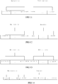
- Fig.11 and 12 are schematic views of an instruction format for performing operations based on two instructions in the present invention.
- Fig. 11 is a format view of bit width configuration instruction.
- the bit width configuration instruction comprises at least one operation code and at least two bit width domains for indicating the bit width of the operator used by the next operation instruction.
- Fig. 12 is a format view of operation instruction.
- the operation instruction comprises at least one operation code and at least 3 operands, wherein the operation code is used to indicate the function of the operation instruction and the operation unit can perform different operations by recognizing one or more operation codes, the operand is used to indicate the data information of the operation instruction; wherein the data information may be an immediate or a register number; for example, to obtain a matrix, a matrix start address and a matrix length can be obtained from the corresponding register according to the register number and then the matrix stored at the corresponding address can be obtained in the storage unit according to the matrix start address and the matrix length.
- Fig.13 ⁇ 14 are instantiations of Figures 11 ⁇ 12 , and are format views of bit width configuration instruction and operation instruction for neural network.
- the bit width configuration instruction comprises at least one operation code and at least four bit width domains for indicating the bit width of the operator used by the next operation instruction for neural network.
- the configuration instruction comprises at least one operation code and 16 operands, wherein the operation code is used to indicate the function of operation the instruction of the neural network and the operation unit can perform different operations for neural network by recognizing one or more operation codes, the operand is used to indicate the data information of operation instruction for the neural network in which the data information may be an immediate or a register number.
- Fig.15 ⁇ 16 are instantiations of Figures 11 ⁇ 12 , and are format views of matrix-matrix bit width configuration instruction and matrix-matrix operation instruction.
- the bit width configuration instruction comprises at least one operation code and at least two bit width domains for indicating the bit width of the operator used by the next matrix-matrix operation instruction.
- the matrix-matrix operation instruction comprises at least one operation code and at least four operands.
- the operation code is used to indicate the function of the matrix-matrix operation instruction and the operation unit can perform different matrix operations by recognizing one or more operation codes
- the operand is used to indicate the data information of matrix-matrix operation instruction in which the data information may be an immediate or a register number.
- Fig.17 ⁇ 18 are instantiations of Figures 11 ⁇ 12 , and are format views of vector-vector bit width configuration instruction and vector-vector operation instruction.
- the bit width configuration instruction comprises at least one operation code and at least two bit width domains for indicating the bit width of the operator used by the next vector-vector operation instruction.
- the vector-vector operation instruction comprises at least one operation code and at least 3 operands, wherein the operation code is used to indicate the function of vector-vector operation instruction and the operation unit can perform different vector operations by recognizing one or more operation codes, the operand is used to indicate the data information of vector-vector operation instruction in which the data information may be an immediate or a register number.
- Fig.19 ⁇ 20 are instantiations of Figures 11 ⁇ 12 , and are format views of matrix-vector bit width configuration instruction and matrix-vector operation instruction.
- the bit width configuration instruction comprises at least one operation code and at least three bit width domains for indicating the bit width of the operator used by the next vector-vector operation instruction.
- the matrix-vector operation instruction comprises at least one operation code and at least 6 operands, wherein the operation code is used to indicate the function of matrix-vector operation instruction and the operation unit can perform different matrix and vector operations by recognizing one or more operation codes, the operand is used to indicate the data information of matrix-vector operation instruction in which the data information may be an immediate or a register number.
- Fig. 21 is a flowchart of an operation performed by the operation device according to embodiments of the present invention using two instructions. As shown in Fig. 21 , the process comprises:
- the present invention discloses a configurable device and method for performing neural network operation and matrix/vector operation, can solve the problem of neural network operation and a large number of matrix/vector operations in the current computer domain with the corresponding instructions.
- the present invention can have instructions configurable, easy to use, wherein the bit width of the operator can be selected and multiple operators can be combined, and the bit width configuration of the operation unit is realized through dedicated bit width configuration instructions and bit width domain specified on the operation instructions. It also has the advantages of the supported neural network scale and matrix/vector bit width and size being flexible, sufficient on-chip caches, and the possibility of combining operation units.
Landscapes
- Engineering & Computer Science (AREA)
- Physics & Mathematics (AREA)
- Theoretical Computer Science (AREA)
- Software Systems (AREA)
- General Physics & Mathematics (AREA)
- General Engineering & Computer Science (AREA)
- Health & Medical Sciences (AREA)
- Life Sciences & Earth Sciences (AREA)
- Biomedical Technology (AREA)
- Biophysics (AREA)
- Mathematical Physics (AREA)
- Neurology (AREA)
- Artificial Intelligence (AREA)
- Computing Systems (AREA)
- General Health & Medical Sciences (AREA)
- Evolutionary Computation (AREA)
- Data Mining & Analysis (AREA)
- Computational Linguistics (AREA)
- Molecular Biology (AREA)
- Computational Mathematics (AREA)
- Mathematical Analysis (AREA)
- Mathematical Optimization (AREA)
- Pure & Applied Mathematics (AREA)
- Executing Machine-Instructions (AREA)
- Complex Calculations (AREA)
- Communication Control (AREA)
Applications Claiming Priority (2)
| Application Number | Priority Date | Filing Date | Title |
|---|---|---|---|
| CN201610640111.8A CN107688854B (zh) | 2016-08-05 | 2016-08-05 | 一种能支持不同位宽运算数据的运算单元、方法及装置 |
| PCT/CN2017/093159 WO2018024093A1 (fr) | 2016-08-05 | 2017-07-17 | Unité de commande, procédé et dispositif aptes à prendre en charge des données de fonctionnement de différentes largeurs de bit |
Publications (3)
| Publication Number | Publication Date |
|---|---|
| EP3496006A1 true EP3496006A1 (fr) | 2019-06-12 |
| EP3496006A4 EP3496006A4 (fr) | 2020-01-22 |
| EP3496006B1 EP3496006B1 (fr) | 2023-12-27 |
Family
ID=61072493
Family Applications (1)
| Application Number | Title | Priority Date | Filing Date |
|---|---|---|---|
| EP17836275.2A Active EP3496006B1 (fr) | 2016-08-05 | 2017-07-17 | Unité de commande, procédé et dispositif aptes à prendre en charge des données de fonctionnement de différentes largeurs de bit |
Country Status (6)
| Country | Link |
|---|---|
| US (1) | US10489704B2 (fr) |
| EP (1) | EP3496006B1 (fr) |
| KR (1) | KR102486029B1 (fr) |
| CN (2) | CN114004349A (fr) |
| TW (1) | TWI789358B (fr) |
| WO (1) | WO2018024093A1 (fr) |
Cited By (3)
| Publication number | Priority date | Publication date | Assignee | Title |
|---|---|---|---|---|
| WO2021046986A1 (fr) * | 2019-09-12 | 2021-03-18 | 东南大学 | Procédé de sélection pour la largeur de bit de calcul d'une matrice de pe à largeur de bits multiples et circuit de commande de précision de calcul |
| EP3842935A1 (fr) * | 2019-12-27 | 2021-06-30 | INTEL Corporation | Systèmes, appareils et procédés pour des opérations de 512 bits |
| CN113469349A (zh) * | 2021-07-02 | 2021-10-01 | 上海酷芯微电子有限公司 | 多精度神经网络模型实现方法及系统 |
Families Citing this family (15)
| Publication number | Priority date | Publication date | Assignee | Title |
|---|---|---|---|---|
| US10657442B2 (en) * | 2018-04-19 | 2020-05-19 | International Business Machines Corporation | Deep learning accelerator architecture with chunking GEMM |
| US11467973B1 (en) * | 2018-09-28 | 2022-10-11 | Amazon Technologies, Inc. | Fine-grained access memory controller |
| CN111290788B (zh) * | 2018-12-07 | 2022-05-31 | 上海寒武纪信息科技有限公司 | 运算方法、装置、计算机设备和存储介质 |
| CN111079912B (zh) * | 2018-10-19 | 2021-02-12 | 中科寒武纪科技股份有限公司 | 运算方法、系统及相关产品 |
| CN111258634B (zh) * | 2018-11-30 | 2022-11-22 | 上海寒武纪信息科技有限公司 | 数据选择装置、数据处理方法、芯片及电子设备 |
| CN111260045B (zh) * | 2018-11-30 | 2022-12-02 | 上海寒武纪信息科技有限公司 | 译码器和原子指令解析方法 |
| KR102393916B1 (ko) * | 2019-06-27 | 2022-05-02 | 주식회사 사피온코리아 | 위노그라드 알고리즘에 기반한 행렬 곱셈 방법 및 장치 |
| CN112286578B (zh) * | 2019-07-25 | 2025-09-12 | 北京百度网讯科技有限公司 | 由计算设备执行的方法、装置、设备和计算机可读存储介质 |
| CN111459546B (zh) * | 2020-03-30 | 2023-04-18 | 芯来智融半导体科技(上海)有限公司 | 一种实现操作数位宽可变的装置及方法 |
| US12112167B2 (en) | 2020-06-27 | 2024-10-08 | Intel Corporation | Matrix data scatter and gather between rows and irregularly spaced memory locations |
| US12474928B2 (en) | 2020-12-22 | 2025-11-18 | Intel Corporation | Processors, methods, systems, and instructions to select and store data elements from strided data element positions in a first dimension from three source two-dimensional arrays in a result two-dimensional array |
| CN114528248A (zh) * | 2022-04-24 | 2022-05-24 | 广州万协通信息技术有限公司 | 阵列重构方法、装置、设备及存储介质 |
| CN115390925A (zh) * | 2022-08-16 | 2022-11-25 | 海光信息技术股份有限公司 | 指令的数据处理方法、相关器件及电子设备 |
| CN116248217B (zh) * | 2022-12-14 | 2026-04-14 | 成都海光集成电路设计有限公司 | 时间同步运算方法、模组及数据传输设备 |
| WO2025118193A1 (fr) * | 2023-12-06 | 2025-06-12 | 声龙(新加坡)私人有限公司 | Appareil et procédé d'accélération de calcul, et puce |
Family Cites Families (18)
| Publication number | Priority date | Publication date | Assignee | Title |
|---|---|---|---|---|
| US5471633A (en) * | 1993-09-30 | 1995-11-28 | Intel Corporation | Idiom recognizer within a register alias table |
| US5590352A (en) * | 1994-04-26 | 1996-12-31 | Advanced Micro Devices, Inc. | Dependency checking and forwarding of variable width operands |
| US6418527B1 (en) * | 1998-10-13 | 2002-07-09 | Motorola, Inc. | Data processor instruction system for grouping instructions with or without a common prefix and data processing system that uses two or more instruction grouping methods |
| JP4475614B2 (ja) * | 2000-04-28 | 2010-06-09 | 大正製薬株式会社 | 並列処理方法におけるジョブの割り当て方法および並列処理方法 |
| US6948051B2 (en) * | 2001-05-15 | 2005-09-20 | International Business Machines Corporation | Method and apparatus for reducing logic activity in a microprocessor using reduced bit width slices that are enabled or disabled depending on operation width |
| JP3497852B1 (ja) * | 2002-06-06 | 2004-02-16 | 沖電気工業株式会社 | 演算方法および演算回路 |
| US8595279B2 (en) * | 2006-02-27 | 2013-11-26 | Qualcomm Incorporated | Floating-point processor with reduced power requirements for selectable subprecision |
| DE602006006990D1 (de) * | 2006-06-28 | 2009-07-09 | St Microelectronics Nv | SIMD-Prozessorarchitektur mit gruppierten Verarbeitungseinheiten |
| CN100456231C (zh) * | 2007-03-19 | 2009-01-28 | 中国人民解放军国防科学技术大学 | 灵活分配运算群资源的流处理器扩展方法 |
| CN102238348B (zh) * | 2010-04-20 | 2014-02-05 | 上海华虹集成电路有限责任公司 | 一种可变数据个数的fft/ifft处理器的基4模块 |
| US20110320765A1 (en) * | 2010-06-28 | 2011-12-29 | International Business Machines Corporation | Variable width vector instruction processor |
| CN102012876B (zh) * | 2010-11-19 | 2015-09-16 | 中兴通讯股份有限公司 | 大位宽数据的写入、读取方法及控制器 |
| CN103188487B (zh) * | 2011-12-28 | 2016-11-23 | 联芯科技有限公司 | 视频图像中的卷积方法及视频图像处理系统 |
| JP5786719B2 (ja) * | 2012-01-04 | 2015-09-30 | 富士通株式会社 | ベクトルプロセッサ |
| CN102591615A (zh) * | 2012-01-16 | 2012-07-18 | 中国人民解放军国防科学技术大学 | 结构化混合位宽乘法运算方法及装置 |
| CN103019647B (zh) * | 2012-11-28 | 2015-06-24 | 中国人民解放军国防科学技术大学 | 具有浮点精度保持功能的浮点累加/累减运算方法 |
| US9389863B2 (en) * | 2014-02-10 | 2016-07-12 | Via Alliance Semiconductor Co., Ltd. | Processor that performs approximate computing instructions |
| CN103914277B (zh) * | 2014-04-14 | 2017-02-15 | 复旦大学 | 一种基于改进的Montgomery模乘算法的可扩展模乘器电路 |
-
2016
- 2016-08-05 CN CN202111234282.8A patent/CN114004349A/zh active Pending
- 2016-08-05 CN CN201610640111.8A patent/CN107688854B/zh active Active
-
2017
- 2017-07-17 KR KR1020187034252A patent/KR102486029B1/ko active Active
- 2017-07-17 WO PCT/CN2017/093159 patent/WO2018024093A1/fr not_active Ceased
- 2017-07-17 EP EP17836275.2A patent/EP3496006B1/fr active Active
- 2017-08-04 TW TW106126470A patent/TWI789358B/zh active
-
2019
- 2019-02-05 US US16/268,457 patent/US10489704B2/en active Active
Cited By (3)
| Publication number | Priority date | Publication date | Assignee | Title |
|---|---|---|---|---|
| WO2021046986A1 (fr) * | 2019-09-12 | 2021-03-18 | 东南大学 | Procédé de sélection pour la largeur de bit de calcul d'une matrice de pe à largeur de bits multiples et circuit de commande de précision de calcul |
| EP3842935A1 (fr) * | 2019-12-27 | 2021-06-30 | INTEL Corporation | Systèmes, appareils et procédés pour des opérations de 512 bits |
| CN113469349A (zh) * | 2021-07-02 | 2021-10-01 | 上海酷芯微电子有限公司 | 多精度神经网络模型实现方法及系统 |
Also Published As
| Publication number | Publication date |
|---|---|
| EP3496006A4 (fr) | 2020-01-22 |
| US20190236442A1 (en) | 2019-08-01 |
| TWI789358B (zh) | 2023-01-11 |
| WO2018024093A1 (fr) | 2018-02-08 |
| KR102486029B1 (ko) | 2023-01-06 |
| TW201805835A (zh) | 2018-02-16 |
| CN114004349A (zh) | 2022-02-01 |
| EP3496006B1 (fr) | 2023-12-27 |
| KR20190029515A (ko) | 2019-03-20 |
| CN107688854A (zh) | 2018-02-13 |
| US10489704B2 (en) | 2019-11-26 |
| CN107688854B (zh) | 2021-10-19 |
Similar Documents
| Publication | Publication Date | Title |
|---|---|---|
| EP3496006A1 (fr) | Unité de commande, procédé et dispositif aptes à prendre en charge des données de fonctionnement de différentes largeurs de bit | |
| EP3451162B1 (fr) | Dispositif et procédé servant à exécuter des opérations de multiplication de matrices | |
| CN107329936A (zh) | 一种用于执行神经网络运算以及矩阵/向量运算的装置和方法 | |
| JP7242998B2 (ja) | ニューロモルフィック・アクセラレータ・マルチタスキング | |
| KR102123633B1 (ko) | 행렬 연산 장치 및 방법 | |
| US11907158B2 (en) | Vector processor with vector first and multiple lane configuration | |
| KR102703934B1 (ko) | 벡터 인덱스 레지스터 | |
| KR100331565B1 (ko) | 매트릭스 연산 장치 및 매트릭스 연산기능을 갖는 디지털신호처리 장치 | |
| CN112633505A (zh) | 一种基于risc-v的人工智能推理方法和系统 | |
| CN107315563A (zh) | 一种用于执行向量比较运算的装置和方法 | |
| CN119939097A (zh) | 一种基于risc-v的矩阵乘加运算实现方法、设备及介质 | |
| CN113874836A (zh) | 真/假向量索引寄存器 | |
| WO2017181336A1 (fr) | Appareil et procédé d'opération de couche "maxout" | |
| CN107315565A (zh) | 一种用于生成服从一定分布的随机向量装置和方法 | |
| US12229587B2 (en) | Command processor, neural core SOC and method for obtaining context data using the same | |
| US20230394293A1 (en) | Neuro-synaptic processing circuitry | |
| CN118259916A (zh) | 编译方法、运行方法及相关产品 | |
| CN117648091A (zh) | 计算图的编译方法及相关产品 | |
| CN112596881A (zh) | 存储部件及人工智能处理器 | |
| EP4206995B1 (fr) | Dispositif de traitement neuronal et procédé de synchronisation de celui-ci | |
| JP2026510037A (ja) | インメモリコンピューティングのためのベクトル処理 | |
| CN117093263A (zh) | 处理器、芯片、板卡及方法 | |
| CN117520254A (zh) | 处理器、芯片、板卡及方法 |
Legal Events
| Date | Code | Title | Description |
|---|---|---|---|
| STAA | Information on the status of an ep patent application or granted ep patent |
Free format text: STATUS: THE INTERNATIONAL PUBLICATION HAS BEEN MADE |
|
| PUAI | Public reference made under article 153(3) epc to a published international application that has entered the european phase |
Free format text: ORIGINAL CODE: 0009012 |
|
| STAA | Information on the status of an ep patent application or granted ep patent |
Free format text: STATUS: REQUEST FOR EXAMINATION WAS MADE |
|
| 17P | Request for examination filed |
Effective date: 20181114 |
|
| AK | Designated contracting states |
Kind code of ref document: A1 Designated state(s): AL AT BE BG CH CY CZ DE DK EE ES FI FR GB GR HR HU IE IS IT LI LT LU LV MC MK MT NL NO PL PT RO RS SE SI SK SM TR |
|
| AX | Request for extension of the european patent |
Extension state: BA ME |
|
| DAV | Request for validation of the european patent (deleted) | ||
| DAX | Request for extension of the european patent (deleted) | ||
| A4 | Supplementary search report drawn up and despatched |
Effective date: 20200102 |
|
| RIC1 | Information provided on ipc code assigned before grant |
Ipc: G06N 3/063 20060101AFI20191217BHEP Ipc: G06F 9/30 20180101ALI20191217BHEP |
|
| STAA | Information on the status of an ep patent application or granted ep patent |
Free format text: STATUS: EXAMINATION IS IN PROGRESS |
|
| 17Q | First examination report despatched |
Effective date: 20200224 |
|
| GRAP | Despatch of communication of intention to grant a patent |
Free format text: ORIGINAL CODE: EPIDOSNIGR1 |
|
| STAA | Information on the status of an ep patent application or granted ep patent |
Free format text: STATUS: GRANT OF PATENT IS INTENDED |
|
| INTG | Intention to grant announced |
Effective date: 20230821 |
|
| GRAS | Grant fee paid |
Free format text: ORIGINAL CODE: EPIDOSNIGR3 |
|
| GRAA | (expected) grant |
Free format text: ORIGINAL CODE: 0009210 |
|
| STAA | Information on the status of an ep patent application or granted ep patent |
Free format text: STATUS: THE PATENT HAS BEEN GRANTED |
|
| AK | Designated contracting states |
Kind code of ref document: B1 Designated state(s): AL AT BE BG CH CY CZ DE DK EE ES FI FR GB GR HR HU IE IS IT LI LT LU LV MC MK MT NL NO PL PT RO RS SE SI SK SM TR |
|
| RAP3 | Party data changed (applicant data changed or rights of an application transferred) |
Owner name: CAMBRICON TECHNOLOGIES CORPORATION LIMITED |
|
| REG | Reference to a national code |
Ref country code: GB Ref legal event code: FG4D |
|
| REG | Reference to a national code |
Ref country code: CH Ref legal event code: EP |
|
| REG | Reference to a national code |
Ref country code: DE Ref legal event code: R096 Ref document number: 602017077978 Country of ref document: DE |
|
| REG | Reference to a national code |
Ref country code: IE Ref legal event code: FG4D |
|
| PG25 | Lapsed in a contracting state [announced via postgrant information from national office to epo] |
Ref country code: GR Free format text: LAPSE BECAUSE OF FAILURE TO SUBMIT A TRANSLATION OF THE DESCRIPTION OR TO PAY THE FEE WITHIN THE PRESCRIBED TIME-LIMIT Effective date: 20240328 |
|
| REG | Reference to a national code |
Ref country code: LT Ref legal event code: MG9D |
|
| PG25 | Lapsed in a contracting state [announced via postgrant information from national office to epo] |
Ref country code: LT Free format text: LAPSE BECAUSE OF FAILURE TO SUBMIT A TRANSLATION OF THE DESCRIPTION OR TO PAY THE FEE WITHIN THE PRESCRIBED TIME-LIMIT Effective date: 20231227 |
|
| PG25 | Lapsed in a contracting state [announced via postgrant information from national office to epo] |
Ref country code: ES Free format text: LAPSE BECAUSE OF FAILURE TO SUBMIT A TRANSLATION OF THE DESCRIPTION OR TO PAY THE FEE WITHIN THE PRESCRIBED TIME-LIMIT Effective date: 20231227 |
|
| PG25 | Lapsed in a contracting state [announced via postgrant information from national office to epo] |
Ref country code: LT Free format text: LAPSE BECAUSE OF FAILURE TO SUBMIT A TRANSLATION OF THE DESCRIPTION OR TO PAY THE FEE WITHIN THE PRESCRIBED TIME-LIMIT Effective date: 20231227 Ref country code: GR Free format text: LAPSE BECAUSE OF FAILURE TO SUBMIT A TRANSLATION OF THE DESCRIPTION OR TO PAY THE FEE WITHIN THE PRESCRIBED TIME-LIMIT Effective date: 20240328 Ref country code: FI Free format text: LAPSE BECAUSE OF FAILURE TO SUBMIT A TRANSLATION OF THE DESCRIPTION OR TO PAY THE FEE WITHIN THE PRESCRIBED TIME-LIMIT Effective date: 20231227 Ref country code: ES Free format text: LAPSE BECAUSE OF FAILURE TO SUBMIT A TRANSLATION OF THE DESCRIPTION OR TO PAY THE FEE WITHIN THE PRESCRIBED TIME-LIMIT Effective date: 20231227 Ref country code: BG Free format text: LAPSE BECAUSE OF FAILURE TO SUBMIT A TRANSLATION OF THE DESCRIPTION OR TO PAY THE FEE WITHIN THE PRESCRIBED TIME-LIMIT Effective date: 20240327 |
|
| REG | Reference to a national code |
Ref country code: NL Ref legal event code: MP Effective date: 20231227 |
|
| REG | Reference to a national code |
Ref country code: AT Ref legal event code: MK05 Ref document number: 1645220 Country of ref document: AT Kind code of ref document: T Effective date: 20231227 |
|
| PG25 | Lapsed in a contracting state [announced via postgrant information from national office to epo] |
Ref country code: NL Free format text: LAPSE BECAUSE OF FAILURE TO SUBMIT A TRANSLATION OF THE DESCRIPTION OR TO PAY THE FEE WITHIN THE PRESCRIBED TIME-LIMIT Effective date: 20231227 |
|
| PG25 | Lapsed in a contracting state [announced via postgrant information from national office to epo] |
Ref country code: SE Free format text: LAPSE BECAUSE OF FAILURE TO SUBMIT A TRANSLATION OF THE DESCRIPTION OR TO PAY THE FEE WITHIN THE PRESCRIBED TIME-LIMIT Effective date: 20231227 Ref country code: RS Free format text: LAPSE BECAUSE OF FAILURE TO SUBMIT A TRANSLATION OF THE DESCRIPTION OR TO PAY THE FEE WITHIN THE PRESCRIBED TIME-LIMIT Effective date: 20231227 Ref country code: NO Free format text: LAPSE BECAUSE OF FAILURE TO SUBMIT A TRANSLATION OF THE DESCRIPTION OR TO PAY THE FEE WITHIN THE PRESCRIBED TIME-LIMIT Effective date: 20240327 Ref country code: NL Free format text: LAPSE BECAUSE OF FAILURE TO SUBMIT A TRANSLATION OF THE DESCRIPTION OR TO PAY THE FEE WITHIN THE PRESCRIBED TIME-LIMIT Effective date: 20231227 Ref country code: LV Free format text: LAPSE BECAUSE OF FAILURE TO SUBMIT A TRANSLATION OF THE DESCRIPTION OR TO PAY THE FEE WITHIN THE PRESCRIBED TIME-LIMIT Effective date: 20231227 Ref country code: HR Free format text: LAPSE BECAUSE OF FAILURE TO SUBMIT A TRANSLATION OF THE DESCRIPTION OR TO PAY THE FEE WITHIN THE PRESCRIBED TIME-LIMIT Effective date: 20231227 |
|
| PG25 | Lapsed in a contracting state [announced via postgrant information from national office to epo] |
Ref country code: IS Free format text: LAPSE BECAUSE OF FAILURE TO SUBMIT A TRANSLATION OF THE DESCRIPTION OR TO PAY THE FEE WITHIN THE PRESCRIBED TIME-LIMIT Effective date: 20240427 |
|
| PG25 | Lapsed in a contracting state [announced via postgrant information from national office to epo] |
Ref country code: CZ Free format text: LAPSE BECAUSE OF FAILURE TO SUBMIT A TRANSLATION OF THE DESCRIPTION OR TO PAY THE FEE WITHIN THE PRESCRIBED TIME-LIMIT Effective date: 20231227 Ref country code: AT Free format text: LAPSE BECAUSE OF FAILURE TO SUBMIT A TRANSLATION OF THE DESCRIPTION OR TO PAY THE FEE WITHIN THE PRESCRIBED TIME-LIMIT Effective date: 20231227 |
|
| PG25 | Lapsed in a contracting state [announced via postgrant information from national office to epo] |
Ref country code: SK Free format text: LAPSE BECAUSE OF FAILURE TO SUBMIT A TRANSLATION OF THE DESCRIPTION OR TO PAY THE FEE WITHIN THE PRESCRIBED TIME-LIMIT Effective date: 20231227 |
|
| PG25 | Lapsed in a contracting state [announced via postgrant information from national office to epo] |
Ref country code: SM Free format text: LAPSE BECAUSE OF FAILURE TO SUBMIT A TRANSLATION OF THE DESCRIPTION OR TO PAY THE FEE WITHIN THE PRESCRIBED TIME-LIMIT Effective date: 20231227 Ref country code: SK Free format text: LAPSE BECAUSE OF FAILURE TO SUBMIT A TRANSLATION OF THE DESCRIPTION OR TO PAY THE FEE WITHIN THE PRESCRIBED TIME-LIMIT Effective date: 20231227 Ref country code: RO Free format text: LAPSE BECAUSE OF FAILURE TO SUBMIT A TRANSLATION OF THE DESCRIPTION OR TO PAY THE FEE WITHIN THE PRESCRIBED TIME-LIMIT Effective date: 20231227 Ref country code: IT Free format text: LAPSE BECAUSE OF FAILURE TO SUBMIT A TRANSLATION OF THE DESCRIPTION OR TO PAY THE FEE WITHIN THE PRESCRIBED TIME-LIMIT Effective date: 20231227 Ref country code: IS Free format text: LAPSE BECAUSE OF FAILURE TO SUBMIT A TRANSLATION OF THE DESCRIPTION OR TO PAY THE FEE WITHIN THE PRESCRIBED TIME-LIMIT Effective date: 20240427 Ref country code: EE Free format text: LAPSE BECAUSE OF FAILURE TO SUBMIT A TRANSLATION OF THE DESCRIPTION OR TO PAY THE FEE WITHIN THE PRESCRIBED TIME-LIMIT Effective date: 20231227 Ref country code: CZ Free format text: LAPSE BECAUSE OF FAILURE TO SUBMIT A TRANSLATION OF THE DESCRIPTION OR TO PAY THE FEE WITHIN THE PRESCRIBED TIME-LIMIT Effective date: 20231227 Ref country code: AT Free format text: LAPSE BECAUSE OF FAILURE TO SUBMIT A TRANSLATION OF THE DESCRIPTION OR TO PAY THE FEE WITHIN THE PRESCRIBED TIME-LIMIT Effective date: 20231227 |
|
| PG25 | Lapsed in a contracting state [announced via postgrant information from national office to epo] |
Ref country code: PT Free format text: LAPSE BECAUSE OF FAILURE TO SUBMIT A TRANSLATION OF THE DESCRIPTION OR TO PAY THE FEE WITHIN THE PRESCRIBED TIME-LIMIT Effective date: 20240429 Ref country code: PL Free format text: LAPSE BECAUSE OF FAILURE TO SUBMIT A TRANSLATION OF THE DESCRIPTION OR TO PAY THE FEE WITHIN THE PRESCRIBED TIME-LIMIT Effective date: 20231227 |
|
| REG | Reference to a national code |
Ref country code: DE Ref legal event code: R097 Ref document number: 602017077978 Country of ref document: DE |
|
| PG25 | Lapsed in a contracting state [announced via postgrant information from national office to epo] |
Ref country code: DK Free format text: LAPSE BECAUSE OF FAILURE TO SUBMIT A TRANSLATION OF THE DESCRIPTION OR TO PAY THE FEE WITHIN THE PRESCRIBED TIME-LIMIT Effective date: 20231227 |
|
| PG25 | Lapsed in a contracting state [announced via postgrant information from national office to epo] |
Ref country code: DK Free format text: LAPSE BECAUSE OF FAILURE TO SUBMIT A TRANSLATION OF THE DESCRIPTION OR TO PAY THE FEE WITHIN THE PRESCRIBED TIME-LIMIT Effective date: 20231227 |
|
| PLBE | No opposition filed within time limit |
Free format text: ORIGINAL CODE: 0009261 |
|
| STAA | Information on the status of an ep patent application or granted ep patent |
Free format text: STATUS: NO OPPOSITION FILED WITHIN TIME LIMIT |
|
| 26N | No opposition filed |
Effective date: 20240930 |
|
| PG25 | Lapsed in a contracting state [announced via postgrant information from national office to epo] |
Ref country code: MC Free format text: LAPSE BECAUSE OF FAILURE TO SUBMIT A TRANSLATION OF THE DESCRIPTION OR TO PAY THE FEE WITHIN THE PRESCRIBED TIME-LIMIT Effective date: 20231227 |
|
| REG | Reference to a national code |
Ref country code: CH Ref legal event code: PL |
|
| PG25 | Lapsed in a contracting state [announced via postgrant information from national office to epo] |
Ref country code: LU Free format text: LAPSE BECAUSE OF NON-PAYMENT OF DUE FEES Effective date: 20240717 |
|
| PG25 | Lapsed in a contracting state [announced via postgrant information from national office to epo] |
Ref country code: LU Free format text: LAPSE BECAUSE OF NON-PAYMENT OF DUE FEES Effective date: 20240717 |
|
| PG25 | Lapsed in a contracting state [announced via postgrant information from national office to epo] |
Ref country code: SI Free format text: LAPSE BECAUSE OF FAILURE TO SUBMIT A TRANSLATION OF THE DESCRIPTION OR TO PAY THE FEE WITHIN THE PRESCRIBED TIME-LIMIT Effective date: 20231227 Ref country code: CH Free format text: LAPSE BECAUSE OF NON-PAYMENT OF DUE FEES Effective date: 20240731 Ref country code: BE Free format text: LAPSE BECAUSE OF NON-PAYMENT OF DUE FEES Effective date: 20240731 |
|
| REG | Reference to a national code |
Ref country code: BE Ref legal event code: MM Effective date: 20240731 |
|
| PG25 | Lapsed in a contracting state [announced via postgrant information from national office to epo] |
Ref country code: IE Free format text: LAPSE BECAUSE OF NON-PAYMENT OF DUE FEES Effective date: 20240717 |
|
| PGFP | Annual fee paid to national office [announced via postgrant information from national office to epo] |
Ref country code: DE Payment date: 20250722 Year of fee payment: 9 |
|
| PGFP | Annual fee paid to national office [announced via postgrant information from national office to epo] |
Ref country code: GB Payment date: 20250722 Year of fee payment: 9 |
|
| PGFP | Annual fee paid to national office [announced via postgrant information from national office to epo] |
Ref country code: FR Payment date: 20250725 Year of fee payment: 9 |
|
| PG25 | Lapsed in a contracting state [announced via postgrant information from national office to epo] |
Ref country code: CY Free format text: LAPSE BECAUSE OF FAILURE TO SUBMIT A TRANSLATION OF THE DESCRIPTION OR TO PAY THE FEE WITHIN THE PRESCRIBED TIME-LIMIT; INVALID AB INITIO Effective date: 20170717 |
|
| PG25 | Lapsed in a contracting state [announced via postgrant information from national office to epo] |
Ref country code: HU Free format text: LAPSE BECAUSE OF FAILURE TO SUBMIT A TRANSLATION OF THE DESCRIPTION OR TO PAY THE FEE WITHIN THE PRESCRIBED TIME-LIMIT; INVALID AB INITIO Effective date: 20170717 |