EP3496111A1 - Rotierende ladungsumwandlungsschicht eines ionenstrahlumwandlers und verfahren zur umwandlung einer ionenstrahlladung - Google Patents
Rotierende ladungsumwandlungsschicht eines ionenstrahlumwandlers und verfahren zur umwandlung einer ionenstrahlladung Download PDFInfo
- Publication number
- EP3496111A1 EP3496111A1 EP17836852.8A EP17836852A EP3496111A1 EP 3496111 A1 EP3496111 A1 EP 3496111A1 EP 17836852 A EP17836852 A EP 17836852A EP 3496111 A1 EP3496111 A1 EP 3496111A1
- Authority
- EP
- European Patent Office
- Prior art keywords
- film
- charge stripping
- stripping film
- charge
- ion beam
- Prior art date
- Legal status (The legal status is an assumption and is not a legal conclusion. Google has not performed a legal analysis and makes no representation as to the accuracy of the status listed.)
- Granted
Links
Images


Classifications
-
- G—PHYSICS
- G21—NUCLEAR PHYSICS; NUCLEAR ENGINEERING
- G21K—HANDLING OF PARTICLES OR IONISING RADIATION NOT OTHERWISE PROVIDED FOR; IRRADIATION DEVICES; GAMMA RAY OR X-RAY MICROSCOPES
- G21K1/00—Arrangements for handling particles or ionising radiation, e.g. focusing or moderating
- G21K1/14—Arrangements for handling particles or ionising radiation, e.g. focusing or moderating using charge exchange devices, e.g. for neutralising or changing the sign of the electrical charges of beams
-
- C—CHEMISTRY; METALLURGY
- C01—INORGANIC CHEMISTRY
- C01B—NON-METALLIC ELEMENTS; COMPOUNDS THEREOF; METALLOIDS OR COMPOUNDS THEREOF NOT COVERED BY SUBCLASS C01C
- C01B32/00—Carbon; Compounds thereof
- C01B32/15—Nano-sized carbon materials
- C01B32/182—Graphene
-
- G—PHYSICS
- G21—NUCLEAR PHYSICS; NUCLEAR ENGINEERING
- G21K—HANDLING OF PARTICLES OR IONISING RADIATION NOT OTHERWISE PROVIDED FOR; IRRADIATION DEVICES; GAMMA RAY OR X-RAY MICROSCOPES
- G21K1/00—Arrangements for handling particles or ionising radiation, e.g. focusing or moderating
-
- G—PHYSICS
- G21—NUCLEAR PHYSICS; NUCLEAR ENGINEERING
- G21K—HANDLING OF PARTICLES OR IONISING RADIATION NOT OTHERWISE PROVIDED FOR; IRRADIATION DEVICES; GAMMA RAY OR X-RAY MICROSCOPES
- G21K5/00—Irradiation devices
- G21K5/08—Holders for targets or for other objects to be irradiated
-
- H—ELECTRICITY
- H05—ELECTRIC TECHNIQUES NOT OTHERWISE PROVIDED FOR
- H05H—PLASMA TECHNIQUE; PRODUCTION OF ACCELERATED ELECTRICALLY-CHARGED PARTICLES OR OF NEUTRONS; PRODUCTION OR ACCELERATION OF NEUTRAL MOLECULAR OR ATOMIC BEAMS
- H05H7/00—Details of devices of the types covered by groups H05H9/00, H05H11/00, H05H13/00
- H05H7/10—Arrangements for ejecting particles from orbits
Definitions
- the present invention relates to a rotary charge stripping film used in a charge stripping device of an ion beam and a charge stripping method using the rotary charge stripping film.
- Non-Patent Document 1 Liquid lithium, beryllium, a carbon film, a carbon-boron composite film, a carbon nanotube composite film, and a carbon-organic composite film have been reported as charge stripping films (Non-Patent Document 1).
- Patent Document 1 also reports that a carbon film is vapor-deposited on a vapor-deposited substrate obtained by vacuum-depositing nickel chloride on a glass substrate by arc discharge or the like, and the film is used as a charge stripping film.
- Patent Document 2 also reports a carbon-boron composite film as a charge stripping film.
- Non-Patent Document 2 carbon nanotube (CNT) composite films as disclosed in Patent Document 3 have high physical strength, they may be broken due to a long-time operation because of a low heat resistance, so that there is a problem in reliability such as necessity to stop the operation of the accelerator at each time (Non-Patent Document 2).
- Non-Patent Document 2 In order to prevent a beam energy after passing through a charge stripping film from decreasing too much, a film thickness of the charge stripping film should be reduced, but on the other hand, when the film thickness becomes thin, a beam after passing through the film is difficult to be made multivalent. Furthermore, since an ion beam has high energy, a load applied to the charge stripping film is large, so that the charge stripping film is required to have durability. In order to improve the durability, attempts have been made to prevent the beam from being intensively irradiated to a specific portion of the charge stripping film by rotating the charge stripping film (Non-Patent Document 2).
- Non-Patent Document 3 is preferable from the viewpoint of durability and stability, but a large-scale device is necessary.
- the charge stripping film of the present invention including a carbon film having a thermal conductivity of 20 W/mK or more in the film surface direction at 25°C can be produced by a polymer annealing method, has no risk of toxicity and activation and can make an ion beam multivalent with a high efficiency.
- the charge stripping film of the present invention can be used as a rotary type, the beam is not irradiated intensively to only one point of the charge stripping film and the charge stripping film can withstand a long-term use.
- the charge stripping of the ion beam can be performed more conveniently than the charge stripping method using a gas stripper.
- the charge stripping film of the present invention including a carbon film having a thermal conductivity of 20 W/mK or more at 25°C in the film surface direction can be produced by a polymer annealing method, that is, a method of heat treating a polymer film.
- the thermal conductivity of the charge stripping film of the present invention is higher than that of the carbon film obtained by the vapor deposition method or the like.
- the "surface" in the film surface direction means a surface perpendicular to the thickness direction of the film.
- a graphite structure is first formed on the outermost surface layer of the polymer carbonized film at the time of the secondary heat treatment, and the graphite structure grows toward the inside of the film.
- the graphite structure becomes more disordered and a cavity or a defect is more likely to arise toward inside the carbon film.
- the graphitization proceeds to inside in a well-ordered state of the graphite layer structure of the film surface, resulting in that a graphite structure that is well-ordered all over the film is likely to be formed. It is considered that the thinner film is easier to arrange the graphite layer structure, and therefore the charge stripping film of the present invention becomes a film showing a high thermal conductivity.
- the charge stripping film of the present invention has a film thickness of 0.2 ⁇ m or more and less than 10 ⁇ m.
- the film thickness of the charge stripping film may be adjusted according to the type and intensity of the beam to be used and the stripping efficiency to the target valence and may be 1 ⁇ m or more, may be more than 3 ⁇ m, may be 4 ⁇ m or more or 5 ⁇ m or more, and may be 8 ⁇ m or less or 9 ⁇ m or less.
- the ion beam is intensively irradiated to one point of the charge stripping film.
- the charge stripping film of the present invention is a rotary type, concentrated irradiation of the ion beam can be prevented, so that the durability of the charge stripping film can be improved.
- the shape of the charge stripping film of the present invention is not particularly limited as long as it can be rotated, and examples thereof include a circular shape, an elliptical shape, a square shape, and the like, but from the viewpoint of ensuring uniformity during rotation, a circular shape is preferable.
- the circular shape means that the outer periphery of the charge stripping film has a circumferential shape, and includes, for example, a shape (donut shape) in which the vicinity of the center of a circle is cut.
- the density of the charge stripping film of the present invention is preferably 0.90 g/cm 3 or more.
- the density of the charge stripping film is preferably large, more preferably 1.5 g/cm 3 or more, further preferably 2.0 g/cm 3 or more, most preferably 2.1 g/cm 3 or more.
- the upper limit of the density is 2.26 g/cm 3 or less and may be 2.20 g/cm 3 or less.
- the area of the charge stripping film of the present invention is preferably 4 cm 2 or more. If the charge stripping film is too small, fixing the charge stripping film to a jig or the like is difficult, and the heat dissipation efficiency is deteriorated. On the other hand, the charge stripping film with a larger area has better thermal diffusivity, and can withstand the high intensity beam over a long period of time.
- the area of the charge stripping film is preferably 9 cm 2 or more, more preferably 16 cm 2 or more, most preferably 25 cm 2 or more. The upper limit of the area is not particularly limited, but it is usually about 900 cm 2 .
- the raw material of the charge stripping film for an ion beam of the present invention is a polymer film as will be described later, and the charge stripping film is never contaminated by impurities including metals during the production process thereof. Also, by annealing the polymer film at a temperature of 2400°C or more as will be described later, nitrogen, oxygen, and hydrogen in the polymer are eliminated and only pure carbon are likely to remain. Therefore, the method of the present invention is a very excellent method for forming a film composed of pure carbon and has a feature of being unlikely to have contaminants other than carbon.
- a laminated structure of plural smooth surfaces of the charge stripping film of the present invention produced by the polymer annealing method is observed in a sectional image obtained by SEM (Scanning Electron Microscope) observation at a magnification of approximately 10,000 to 20,000 times.
- the carbon mass is preferably, for example, 0.2 mg/cm 2 or more and less than 2.2 mg/cm 2 , more preferably 0.25 mg/cm 2 or more and 2.0 mg/cm 2 or less, further preferably 0.3 mg/cm 2 or more and 2.0 mg/cm 2 or less.
- the charge stripping film for an ion beam of the present invention adjusted to have an intended thickness may be used alone (single layer body), or two or more films may be laminated to adjust into an intended thickness (laminated body).
- the charge stripping film for an ion beam of the present invention charge stripping films with various thicknesses that are optimum for the desired beam valence can be easily produced only by changing the combination of the charge stripping films for an ion beam having different thicknesses.
- the charge stripping film may be used as a laminate in close contact with each other or may be arranged independently one by one in the traveling direction of the beam. Even when the charge stripping films of the present invention are used as a laminate, they are used as a charge stripping film with a total thickness of 0.2 ⁇ m or more (preferably more than 3 ⁇ m) and less than 10 ⁇ m. Also, in the case of arranging the charge stripping films one by one independently, if the interval is too small, heat is likely to be trapped between the charge stripping films at the time of irradiation with a beam, and the possibility of damage arises. Therefore, in using two or more films, it is preferable to use the films as a laminate by bringing the films into close contact with each other.
- the thickness of the charge stripping film may be precisely controlled.
- the thickness may be precisely controlled by forming a carbon film (carbonaceous film) on the charge stripping film for an ion beam of the present invention by vapor deposition, sputtering or the like.
- the incident ion beam can be sufficiently converted into multivalence.
- the uranium beam of 64+ can be converted so that the peak of the valence is in the range of 70+ or more, preferably 74+ or more, more preferably 78+ or more and 82+ or less, preferably 81+ or less.
- the charge stripping film of the present invention is produced by a polymer annealing method and is a rotary type, pinholes, chipping or the like does not occur even when a high thermal load is applied.
- occurrence of pinholes and chipping can be prevented even when a thermal load of 0.1 W or more, preferably 4 W or more, more preferably 5 W or more, or further preferably 6 W or more is applied.
- the upper limit of the thermal load that can prevent occurrence of pinholes and chipping is, for example, 22 W or less.
- polyimide film having a polymer structure having a very rigid structure has higher orientation and in view of the availability
- pyromellitic anhydride and 3,3',4,4'-biphenyltetracarboxylic dianhydride are particularly preferred.
- Diamines which can be used for the synthesis of the aromatic polyimide include 4,4'-diaminodiphenyl ether, p-phenylenediamine, 4,4'-diaminodiphenylpropane, 4,4'-diaminodiphenylmethane, benzidine, 3,3'-dichlorobenzidine, 4,4'-diaminodiphenyl sulfide, 3,3'-diaminodiphenyl sulfone, 4,4'-diaminodiphenyl sulfone, 4,4'-diaminodiphenyl ether, 3,3'-diaminodiphenyl ether, 3,4'-diaminodiphenyl ether, 1,5-diaminonaphthalene, 4,4'-diaminodiphenyldiethylsilane, 4,4'-diaminodiphenylsilane, 4,4'-di
- the aromatic polyimide is particularly preferably synthesized by using 4,4'-diaminodiphenylether or p-phenylenediamine as a raw material.
- polyamic acid For the preparation of polyamic acid from the acid dianhydride and diamine, a known method can be used, and normally, at least one kind of acid dianhydrides and at least one kind of diamines are dissolved in an organic solvent, and the obtained solution of polyamic acid in organic solvent is stirred under a controlled temperature condition until polymerization between the acid dianhydride and the diamine completes.
- These polyamic acid solutions are usually obtained at a concentration of 5% by mass or more and 35% by mass or less, preferably 10% by mass or more and 30% by mass or less. When the concentration falls within this range, an appropriate molecular weight and solution viscosity can be obtained.
- the molar amounts of the acid dianhydride and the diamine in the raw material solution are preferably adjusted to be substantially equal, and the molar ratio of the acid dianhydride to the diamine (acid dianhydride/diamine) is, for example, 1.5/1 or less and 1/1.5 or more, preferably 1.2/1 or less and 1/1.2 or more, more preferably 1.1/1 or less and 1/1.1 or more.
- the polymer film can be produced from the polymer raw material or a synthetic raw material thereof by various known techniques.
- a heat curing method in which a polyamic acid as a precursor is converted into imide by heating
- a chemical curing method in which a polyamic acid is converted into imide by using a dehydrating agent typified by acid anhydride such as acetic anhydride, or tertiary amines such as picoline, quinoline, isoquinoline, and pyridine as an imidization promoting agent are known, and any of these methods can be used.
- the polyimide film is produced by casting a solution of polyamic acid, which is the aforementioned polyimide precursor, in an organic solvent, on a support such as an endless belt or a stainless drum and drying to allow imidization.
- a stoichiometric quantity or more of a dehydrating agent, and a catalytic amount of an imidization promoting agent are added, and the solution is casted or applied on a support plate or an organic film of PET or the like, or a support such as a drum or an endless belt, to give a film form, and the organic solvent is evaporated to give a film having self-supportability.
- the thickness of the film can be freely changed depending on the valence of the original beam, the valence of the beam after charge stripping, and the kind of beam.
- the polymer annealing method it is possible to freely vary the thickness of the obtainable charge stripping film for an ion beam by controlling the film thickness of the polymer film as a raw material, and it is further possible to easily vary the area or the shape.
- the polymer annealing method is very suitable method for producing a charge stripping film.
- a polymer film as a starting material is preheated in an inert gas or in a vacuum to be carbonized.
- the inert gas nitrogen, argon or a mixed gas of argon and nitrogen is preferably used.
- the preheating is generally conducted at about 1000°C.
- the heating rate to the preheating temperature is not particularly limited, but can be, for example, 5°C/minute or more and 15°C/minute and less.
- it is effective to apply a pressure in the vertical direction on a film surface to such an extent that breakage of the film does not occur so as to prevent the orientation of the starting polymer film from being lost.
- This treatment temperature may be the maximum treatment temperature in the secondary heat treatment process and the obtained charge stripping film may be reheated in the form of annealing.
- a current is directly applied to a graphite heater, and heating is conducted by utilizing the Joule heat.
- the secondary heat treatment is conducted in an inert gas
- argon is the most appropriate as an inert gas, and a small amount of helium may be added to argon.
- the higher treatment temperature can obtain the graphite with a higher quality by conversion, however, an excellent charge stripping film for an ion beam is obtained even when the treatment temperature is, for example, 3700°C or less, particularly, 3600°C or less, or 3500°C or less.
- the heating rate from the preheating temperature (primary heat treatment temperature) to the secondary heat treatment temperature can be, for example, 1°C/minute or more and 25°C/minute or less.
- the retention time at the treatment temperatures is, for example, 10 minutes or more, preferably 30 minutes or more, and may be 1 hour or more.
- the upper limit of the retention time is not particularly limited, but may be generally 10 hours or less, particularly about 5 hours or less.
- the pressure (gauge pressure) of atmosphere in the high-temperature furnace by the inert gas is, for example, 0.05 MPa or more, preferably 0.10 MPa or more, more preferably 0.14 MPa or more.
- the upper limit of the pressure of atmosphere is not particularly limited, it may be, for example, 2 MPa or less, particularly, about 1.8 MPa or less.
- the temperature can be lowered at a rate of, for example, 30°C/minute or more and 50°C/minute or less.
- Fig. 1 is a schematic view showing one example of a charge stripping method of an ion beam using a charge stripping film.
- the charge stripping method of an ion beam shown in Fig. 1 includes charge stripping films 10a and 10b for removing electrons from an incident ion beam, electromagnets 11a and 11b for converging beams, a bending magnet 12 for bending a beam track, and beam profile detectors 13a and 13b.
- the charge stripping method of the present invention is not limited to the configuration shown in Fig. 1 , but when stripping the charge of the ion beam by irradiating the rotary charge stripping film of the present invention with the ion beam, the ion beam is irradiated to the charge stripping film which is rotating. More specifically, the charge stripping film of the present invention is placed on the ion beam path such that the ion beam is irradiated to a part of the charge stripping film of the present invention in a state before rotation, the charge stripping film is then rotated, and the ion beam is irradiated to the rotating charge stripping film.
- the arrangement of the charge stripping film is determined such that the charge stripping film always intersects the ion beam path during rotation, and it is preferable that the ion beam is irradiated to the peripheral edge portion of the charge stripping film.
- the peripheral edge portion refers to a portion inside the inscribed circle C of the charge stripping film (in the case where the charge stripping film is circular, the inscribed circle C is equal to the circle of the charge stripping film), the portion excluding the rotation center.
- the peripheral edge portion is a region sandwiched between the circumference of a circle A which is a concentric circle of the inscribed circle C and whose radius is 1/4 of the radius of the circle C, and the circumference of a circle B which is a concentric circle of circle C and whose radius is 7/8 of the radius of circle C.
- the charge stripping film as a rotary type, the ion beam is not concentrated on one point of the charge stripping film during irradiation, so that the durability of the charge stripping film is improved.
- the rotation speed of the charge stripping film of the present invention is, for example, 1 rpm or more and 3000 rpm or less.
- the rotation speed is preferably 100 rpm or more, more preferably 500 rpm or more and is preferably 2500 rpm or less, more preferably 2000 rpm or less.
- the charge stripping is preferably carried out under a vacuum environment, and the degree of vacuum is preferably 1 ⁇ 10 -3 Pa or less, more preferably 5 ⁇ 10 -4 Pa or less, further preferably 1 ⁇ 10 -4 Pa or less.
- the lower limit of the degree of vacuum is not particularly limited, but is for example 1 ⁇ 10 -9 Pa.
- electromagnets for converging a beam can be arranged on the upstream side of the charge stripping film and can be arranged particularly on the upstream side of the charge stripping film 10b.
- the ion beam incident from the upstream side of the device (for example, U 64+ etc.) 14 is converged by a beam converging electromagnet as needed and passes through the charge stripping film 10a and/or 10b, and the track of the ion beam is bent by the bending magnet 12.
- ions 15a having a specific valence pass through the bending magnet 12, and beams 15b and 15c having other valences collide with a wall surface of a vacuum box of the bending magnet 12 and disappear.
- the beam converging electromagnet 11b can be arranged, and the beam passing through the electromagnet 11b for converging the beam is then further accelerated by a ring cyclotron (not illustrated).
- the beam profile and the valence distribution of ions can be detected by the beam profile detector 13a between the bending magnet 12 and the electromagnet 11b for converging the beam, or by the beam profile detector 13b on the downstream side of the electromagnet 11b for converging the beam.
- the rotary charge stripping film 23 is fixed at the center by using a circular substrate 21 for fixing a charge stripping film, a circular substrate 22 for supporting a charge stripping film, and a circular substrate 24 for fixing a charge stripping film.
- a structure in which the rotary charge stripping film 23 is rotated by using a bearing or directly connecting to a motor may be adopted.
- the shapes of the substrate 21 for fixing a charge stripping film, the substrate 22 for supporting a charge stripping film, and the substrate 24 for fixing a charge stripping film are not particularly limited as long as each member can be bonded.
- the rotary charge stripping film 23 is described as a single sheet (single layer), but the number of the charge stripping films 23 is not particularly limited, and the carbon film of the present invention may be laminated, or the carbon film of the present invention and the carbon film produced by a method other than the polymer annealing method may be laminated. In addition, at least one layer of a metal and a metal oxide may be laminated on the carbon film of the present invention, or a graphite layer having a different orientation may be further laminated.
- the total thickness of the charge stripping film may be controlled by a method of adjusting the number of carbon films depending on the type of beam to be used and the desired charge.
- the charge stripping film may be pressed and flattened, or a plurality of charge stripping films may be laminated, and the charge stripping films may be brought into close contact with each other using a room temperature press, a heat press, an ultrahigh temperature heat press or the like. Further, a plurality of charge stripping films may be arranged with a space in the traveling direction of the beam.
- the charge stripping films may be brought into close contact with each other by applying a coal pitch, a polymer material or the like to a charge stripping film, laminating a plurality of charge stripping films thereon, room temperature pressing or heat pressing, and heating graphitization with ultrahigh temperature treatment or ultrahigh temperature heat press.
- the thermal diffusivity of the charge stripping film was measured at 25°C in vacuum (about 10 -2 Pa) under a frequency of 10 Hz using a thermal diffusivity measuring device based on the periodic heating method ("LaserPit" device, manufactured by ULVAC-RIKO, Inc.).
- a thermocouple is attached at a point apart by a certain distance from a point irradiated with a laser beam to be heated, and the temperature change of the thermocouple is measured.
- the thermal conductivity (W/mK) was calculated by multiplying thermal diffusivity (m 2 /s), density (kg/m 3 ), and specific heat (798 kJ/(kg ⁇ K)).
- the thermal diffusivity of the charge stripping films D and E having a thickness of 2 ⁇ m or less was measured using a periodical heating radiant temperature measuring (Thermo Analyzer TA3 manufactured by BETHEL Co., Ltd.). This is a device that performs periodic heating with a laser and temperature measurement with a radiation thermometer, and this device is completely non-contact with the graphite sheet at the time of measurement, so it is possible to measure even using a sample with a graphite sheet thickness of 1 ⁇ m or less.
- the thermal conductivity (W/mK) of the charge stripping films D and E each having a thickness of 2 ⁇ m or less was calculated by multiplying thermal diffusivity (m 2 /s), density (2.26 kg/m 3 , theoretical value not including errors due to wrinkles), and specific heat (716 kJ/(kg ⁇ K)).
- the carbon atomic concentration of the produced carbon films A to C was measured by a scanning electron microscope (SEM) SU4600 manufactured by Hitachi High-Technologies Corporation, and a large-diameter SDD detector (EDX-XMax) manufactured by HORIBA, Ltd.
- SEM scanning electron microscope
- EDX-XMax large-diameter SDD detector
- the carbon atomic concentration of the carbon films D and E produced was measured using ULTRAPLUS manufactured by Zeiss, and XFlash 6
- the charge stripping film was analyzed at an accelerating voltage of 10 kV, and the carbon atomic concentration was determined by carbon atomic concentration (%) calculated after the analysis by attached software.
- a hardener containing 20 g of acetic anhydride and 10 g of isoquinoline was mixed with 100 g of an 18% by mass DMF (N,N-dimethylformamide) solution of a polyamic acid synthesized from pyromellitic acid anhydride, and 4,4'-diaminodiphenyl ether at a molar ratio of 1/1, or from pyromellitic anhydride, 4,4'-diaminodiphenyl ether and p-phenylenediamine at a molar ratio of 5/4/1, and the obtained mixture was stirred, centrifuged to be defoamed, and then cast and applied on an aluminum foil.
- DMF N,N-dimethylformamide
- the process from stirring to defoaming was conducted under cooling at 0°C. After heating the resultant laminate of the aluminum foil and the polyamic acid solution at 120°C for 150 seconds, and at 300°C, 400°C, and 500°C for 30 seconds each, the aluminum foil was removed to prepare polyimide films each having different thicknesses. Regarding the thickness of the polyimide film, five kinds of films each having a different thickness in the range of 2 ⁇ m, 4 ⁇ m, 10 ⁇ m, 25 ⁇ m, and 75 ⁇ m were produced by adjusting the casting speed or the like.
- Table 1 shows measurement results of film thickness, density, mass per unit area, thermal conductivity, and carbon atomic concentration of the charge stripping films A to E.
- Table 1 Charge Stripping Film Thickness ( ⁇ m) Density (g/cm 3 ) Mass per Unit Area (mg/cm 2 ) Thermal Conductivity (W/mK) Carbon Atomic Concentration (%) A 4 2.23 0.91 1550 >99 B 10 2.20 2.2 1480 >99 C 35 2.00 7 1500 >99 D 1 2.26 0.23 1200 >99 E 2 2.26 0.45 1500 >99 Vapor-deposited Fil m for Comparison 7.5 about 2 1.5 - - Arizona Film 1 5 about 2 1 - 98 Arizona Film 2 14 about 2 2.8 13 94
- the cross section of the charge stripping film was observed with a scanning electron microscope (SEM) at a magnification of 15000 times. The observed photograph is shown in Fig. 4 .
- SEM scanning electron microscope
- a laminated structure of a plurality of smooth surfaces is observed from Fig. 4 .
- the charge stripping films A to E, and a vapor deposition film for comparison, an Arizona film 1 (XCF manufactured by Arizona Carbon Co., Ltd.) for comparison, and an Arizona film 2 (PCG manufactured by Arizona Carbon Co., Ltd.) for comparison were evaluated by (1) durability of the charge stripping film when rotated at high speed or durability of the charge stripping film when irradiated with calcium ion beam and uranium beam, (2) charge stripping rate of calcium ion beam and uranium ion beam, and (3) convergence of uranium beam after passing through the charge stripping film.
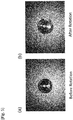
- a charge stripping film D (thickness 1 ⁇ m) cut out into a size of ⁇ 55 mm was attached to the holder shown in Fig. 2 (the material of the substrate 21 for fixing a charge stripping film was aluminum, and the outer diameter was 35 mm) and rotated at 1000 rpm for 44 minutes while changing the rotation speed from 100 rpm to 200 rpm, 300 rpm, 500 rpm, 750 rpm, and 1000 rpm in this order.
- the appearance photographs before and after rotating are shown in Fig. 5.
- Fig. 5(a) is a photograph of external appearance before being rotated
- Fig. 5(b) is a photograph of external appearance after being rotated.
- distortion, damage, and the like were not confirmed even after the charge stripping film of the present invention was rotated at a high speed of 1,000 rpm and the same external appearance as before the rotation was maintained.
- the calcium ion beam was irradiated to the charge stripping film B rotated at a minimum rotation speed of 300 rpm using the holder shown in Fig. 2 for a total of 236 hours.
- the thermal load on the charge stripping film at this current value was 6.366 W and the total number of irradiation particles of calcium was 3.31 ⁇ 10 18 .
- Photographs of the film before and after irradiation are shown in Fig. 6 .
- the film after the beam irradiation was slightly deformed in the vicinity of the beam irradiation position and there was no big difference from before use, and furthermore pinholes, chipping, and the like could not be confirmed.
- a calcium ion beam similar to that of Reference Example 1-1 was used except that the beam current in Reference Example 1-1 was changed to about 4.5 e ⁇ A and the irradiation time in Reference Example 1-1 was changed to 336.7 hours, and a vapor deposition film for comparison having a weight per unit area of about 1.5 mg/cm 2 (thickness is about 7.5 ⁇ m) prepared by a vapor deposition device having a magnetron sputtering source was used in a stationary manner as a charge stripping film. Physical properties of the vapor deposition film for comparison are as shown in Table 1.
- Fig. 7 shows photographs of the charge stripping film before and after irradiation. A big wrinkle was in the vicinity of a beam irradiation spot 1, the film was greatly distorted due to the wrinkle, and an irradiation spot 2 was broken during use.
- Example 1-2 Reference Example 1-2, Example 1-2, and Example 1-3
- the charge stripping films A, B, and E (the material of the substrate 22 for supporting the charge stripping film is copper, and the outer diameter is ⁇ 65 mm to ⁇ 75 mm) rotated by using the holder shown in Fig. 2 were irradiated with a uranium ion beam (U 64+ ) of an irradiation energy of 50 MeV/u, and a beam current of about 1 to 10 e ⁇ A.
- Example 1-2 is an example in which the uranium ion beam was irradiated to the charge stripping film A rotated at 300 rpm for 2 hours and then the charge stripping film A was rotated at 1000 rpm to be further irradiated for 5 minutes.
- Reference Example 1-2 is an example in which a uranium ion beam was irradiated to the charge stripping film B rotated at 300 rpm for 5 minutes.
- Example 1-3 is an example in which a DC beam of U 64+ (uranium) was gradually irradiated to the charge stripping film E rotated at 1000 rpm while increasing the beam current and irradiated for about 3 minutes (maximum beam current: 1 e ⁇ A).
- the thermal load on the graphite film at this current value was 8.9 W in Reference Example 1-2, 21 W in Example 1-2, and 0.4 W in Example 1-3. Photographs of the film before and after irradiation are shown in Figs. 8 and 9 .
- Example 8(a) and 8(b) are photographs of Example 1-2 (charge stripping film A), and Figs. 8(c) and 8(d) are photographs of Reference Example 1-2 (charge stripping film B), and Fig. 9 is a photograph of Example 1-3.
- the film after the beam irradiation was slightly deformed in the vicinity of the beam irradiation position, and there was no big difference from before use, and furthermore pinholes, chipping, and the like could not be confirmed.
- Fig. 9 in the observation after the beam irradiation, even the irradiation traces of the beam could not be confirmed, and the same state as before the beam irradiation was maintained.
- the rotary charge stripping film of the present invention is a thin film having a thickness of less than 10 ⁇ m
- the charge stripping film is excellent in physical strength.
- the rotary charge stripping film with a thickness of 4 ⁇ m did not break in Example 1 even if the beam irradiation was continued while increasing the rotation gradually from 300 rpm and rotating at 1,000 rpm for 5 minutes.
- Increasing the rotation speed is extremely preferable in the point such that the deformation of the charge stripping film due to the heat cycle can be suppressed since the temperature difference in the superheating-cooling process by the irradiation of the high-intensity beam becomes small.
- Evaluation of the charge stripping rate was carried out by irradiating the charge stripping film A disposed at the position 10b shown in Fig. 1 , with a Ca 16+ (calcium) DC beam having a beam current of about 10 e ⁇ A, a beam energy of 45 MeV/u, and a beam shape of 4 to 5 mm in diameter using an accelerator of Nishina Center for Accelerator-Based Science, RIKEN, Japan (Example 2-1).
- the degree of vacuum during charge stripping was 1 ⁇ 10 -3 Pa or less
- the size of the charge stripping film was a circular shape having ⁇ 11 cm
- the minimum rotation speed of the charge stripping film was 300 rpm.
- the stationary vapor deposition film for comparison used in Comparative Example 1 was also subjected to charge stripping.
- Example 2-1 Stripping efficiency to Ca 20+ of Example 2-1 (charge stripping film A) was about 87%, whereas the stripping efficiency to Ca 20+ of the charge stripping film of Comparative Example 2-1 was about 84%. It is understood that the efficiency of the charge stripping film of the invention is about 3% better than the efficiency of the charge stripping film of Comparative Example 2-1. The reason for this is considered to be that the charge stripping film of the present invention has a higher carbon density. Further, although the charge stripping film of the present invention is a rotary type, it has been confirmed that the charge stripping distribution does not widen as compared with the charge stripping film of the stationary type in comparative example. This is thought to be due to the high thickness uniformity of the charge stripping film of the present invention.
- the degree of vacuum during charge stripping was 1 ⁇ 10 -3 Pa or less, the size of the charge stripping film was a circular shape having ⁇ 11 cm, and the minimum rotation speed of the charge stripping film was 300 rpm.
- a charge stripping film B (10 ⁇ m, Reference Example 2-1) and a film obtained by laminating two charge stripping films C to make it 70 ⁇ m (Reference Example 2-2) were also subjected to charge stripping in a rotary manner.
- an evaporated film (Arizona films 1 and 2 listed in Table 1) purchased from Arizona Carbon Foil Co. Inc., USA, was subjected to charge stripping in a stationary manner (Comparative Examples 2-2, 2-3).
- Fig. 10 shows the production ratios of uranium ion beams of respective valences obtained after the U 64+ beam passed through the charge stripping films.
- the peak valence of the uranium beam, obtained by passing through the charge stripping film A of Example 2-2 and the charge stripping film E of Example 2-3, is 78+ and 74+, respectively. In both cases, the generated intensity is sufficiently high, and the width of valence distribution is sufficiently narrow. These effects are more conspicuous in the charge stripping film A as compared with the charge stripping film E.
- the peak valence of the charge stripping film B of Reference Example 2-1 was 82+
- the peak valence of an example in which the charge stripping film C of Reference Example 2-2 was laminated was 87+, and it is understood that the valence can be easily controlled by the film thickness.
- the charge stripping film of the present invention is a rotary type
- the charge stripping distribution does not spread wider than that of the stationary charge stripping film of comparative example. This is thought to be due to the high thickness uniformity of the charge stripping film of the present invention.
- the generation rate of peak valence is slightly higher than in other examples. This is because uranium nuclei are likely to exist in 10 electrons (82+) due to the shell effect of the nucleus.
- the charge stripping film is applicable also to various ion beams.
- the convergence of the ion beam was evaluated by irradiating the charge stripping films A, B and C individually disposed at 10b shown in Fig.1 , with a U 64+ (uranium) DC beam having a beam current (maximum value) of about 10 e ⁇ A and a beam energy of 50 MeV/u, using an accelerator of Nishina Center for Accelerator-Based Science, RIKEN, Japan, and by using a profile monitor of the shape shown in Fig. 11 at positions 13a and 13b in Fig. 1 .
- the degree of vacuum was 1 ⁇ 10 -3 Pa or less, the diameter of the charge stripping film was 11 cm, and the number of revolutions was 300 rpm.
- the holder shown in Fig. 2 was used.
- the profile monitor is a device in which a beam is cut in round slices with a wire and then scanned.
- the profile monitor 30 shown in Fig. 9 is a device for observing a shape of an ion beam, including two orthogonal wire sensors 31a and 31b, and a wire sensor 32 forming an angle of 45 degrees with these two wire sensors, these sensors being attached to a substantially Y-shaped jig 33. Convergence can be evaluated by drawing a graph by plotting the relationship between the position of the wire touched by the beam and the current value at that time and comparing the graph. The scanning with the wire sensor was performed in three different directions, including vertical, horizontal, and diagonal 45 degrees directions.
- the wire of the profile monitor is a ribbon wire of tungsten (manufactured by The Nilaco Corporation), and the wire sensors 31a and 31b in Fig. 9 were each 0.3 mm in thickness, 3 mm in width, and 92 mm in length, and the wire sensor 32 was 0.3 mm in thickness, 3 mm in width, and 65 mm in length.
- the beam profile fluctuation in the lateral direction synchronized with the rotation (the profile fluctuates in the axial direction of at least one of longitudinal, lateral, and oblique axes in the beam profile) is observed.
- an asymmetric shape is drawn. Even if the charge stripping film A of the present invention is irradiated with a beam while rotating at 300 rpm, the beam profile measured at the positions 13a and 13b in Fig. 1 does not move laterally, and asymmetry of the beam profile synchronized with rotation was not observed (the same is true for the charge stripping films B and C).
- the charge stripping film of the present invention has good uniformity of the film thickness distribution and has few large or small unevenness even if it has a large area. Even if the charge stripping film A of the present invention was irradiated with a beam for 2 hours, a large change in the beam profile shape could not be confirmed.
- the uniformity of the film thickness distribution of the charge stripping film of the present invention is very high, and the charge stripping film of the present invention is a material very suitable as a charge stripping film which can withstand use even for a long time.
- the charge stripping film of the present invention can be preferably used as a charge stripping film for use not only in a large-size accelerator, but also in a medical accelerator such as an accelerator for cancer therapy and in a relatively small-size accelerator for industrial use or the like.
Landscapes
- Physics & Mathematics (AREA)
- Engineering & Computer Science (AREA)
- Chemical & Material Sciences (AREA)
- General Engineering & Computer Science (AREA)
- High Energy & Nuclear Physics (AREA)
- Organic Chemistry (AREA)
- Spectroscopy & Molecular Physics (AREA)
- Materials Engineering (AREA)
- Nanotechnology (AREA)
- Inorganic Chemistry (AREA)
- Plasma & Fusion (AREA)
- Carbon And Carbon Compounds (AREA)
Applications Claiming Priority (2)
| Application Number | Priority Date | Filing Date | Title |
|---|---|---|---|
| JP2016154299 | 2016-08-05 | ||
| PCT/JP2017/027254 WO2018025746A1 (ja) | 2016-08-05 | 2017-07-27 | イオンビーム荷電変換装置の回転式荷電変換膜及びイオンビーム荷電変換方法 |
Publications (3)
| Publication Number | Publication Date |
|---|---|
| EP3496111A1 true EP3496111A1 (de) | 2019-06-12 |
| EP3496111A4 EP3496111A4 (de) | 2020-04-22 |
| EP3496111B1 EP3496111B1 (de) | 2026-05-06 |
Family
ID=61073968
Family Applications (1)
| Application Number | Title | Priority Date | Filing Date |
|---|---|---|---|
| EP17836852.8A Active EP3496111B1 (de) | 2016-08-05 | 2017-07-27 | Rotierende stripperfolie in strippervorrichtung eines ionenstrahls und stripperverfahren eines ionenstrahls |
Country Status (5)
| Country | Link |
|---|---|
| US (1) | US11581105B2 (de) |
| EP (1) | EP3496111B1 (de) |
| JP (1) | JP6968372B2 (de) |
| CN (1) | CN109564789B (de) |
| WO (1) | WO2018025746A1 (de) |
Families Citing this family (1)
| Publication number | Priority date | Publication date | Assignee | Title |
|---|---|---|---|---|
| CN114466501A (zh) * | 2022-02-16 | 2022-05-10 | 中国原子能科学研究院 | 一种松弛方法 |
Family Cites Families (14)
| Publication number | Priority date | Publication date | Assignee | Title |
|---|---|---|---|---|
| JPS5523035A (en) | 1978-08-04 | 1980-02-19 | Japan Atom Energy Res Inst | Production of electric charge conversion carbon thin film |
| JP5309320B2 (ja) | 2005-11-15 | 2013-10-09 | 大学共同利用機関法人 高エネルギー加速器研究機構 | 炭素フォイルの作製方法、炭素フォイル、この炭素フォイルを利用した荷電変換用ストリッパーフォイル、及び炭素フォイルの作製装置 |
| JP2007137690A (ja) | 2005-11-15 | 2007-06-07 | High Energy Accelerator Research Organization | 炭素フォイルのビルドアップ抑制方法、炭素フォイル及び炭素フォイルのビルドアップ抑制装置 |
| JP4821011B2 (ja) | 2007-09-27 | 2011-11-24 | 大学共同利用機関法人 高エネルギー加速器研究機構 | 荷電変換薄膜および粒子加速器 |
| EP2129193A1 (de) * | 2008-05-30 | 2009-12-02 | Ion Beam Applications S.A. | Abstreifelement, Abstreifanordnung und Verfahren zur Extraktion eines Partikelstrahls aus einem Zyklotron |
| JP4756285B2 (ja) | 2009-04-23 | 2011-08-24 | 独立行政法人産業技術総合研究所 | 荷電変換用デバイス |
| JP5031796B2 (ja) | 2009-06-11 | 2012-09-26 | 住友重機械工業株式会社 | 粒子加速システム |
| JP2012099354A (ja) * | 2010-11-02 | 2012-05-24 | Sumitomo Heavy Ind Ltd | 粒子加速器及びbnct装置 |
| WO2013043930A1 (en) | 2011-09-20 | 2013-03-28 | Muons, Inc. | Method and apparatus for negative hydrogen ion (h-) stripping innovations for multi-turn injection |
| EP3050845B1 (de) * | 2013-09-26 | 2021-04-21 | Kaneka Corporation | Graphitfolie, verfahren zur herstellung davon, laminatplatte zur verdrahtung, graphitverdrahtungsmaterial und verfahren zur herstellung einer leiterplatte |
| WO2016088845A1 (ja) * | 2014-12-04 | 2016-06-09 | 株式会社カネカ | 高真空用層間熱接合性グラファイトシート |
| JP6683687B2 (ja) | 2015-04-15 | 2020-04-22 | 株式会社カネカ | イオンビームの荷電変換方法 |
| JP6968364B2 (ja) | 2015-04-15 | 2021-11-17 | 株式会社カネカ | イオンビーム荷電変換装置の荷電変換膜及びその製造方法 |
| US11177116B2 (en) | 2016-04-28 | 2021-11-16 | Kaneka Corporation | Beam intensity converting film, and method of manufacturing beam intensity converting film |
-
2017
- 2017-07-27 US US16/320,340 patent/US11581105B2/en active Active
- 2017-07-27 EP EP17836852.8A patent/EP3496111B1/de active Active
- 2017-07-27 JP JP2018531861A patent/JP6968372B2/ja active Active
- 2017-07-27 CN CN201780048733.4A patent/CN109564789B/zh active Active
- 2017-07-27 WO PCT/JP2017/027254 patent/WO2018025746A1/ja not_active Ceased
Also Published As
| Publication number | Publication date |
|---|---|
| WO2018025746A1 (ja) | 2018-02-08 |
| JP6968372B2 (ja) | 2021-11-17 |
| US20190237212A1 (en) | 2019-08-01 |
| EP3496111B1 (de) | 2026-05-06 |
| CN109564789B (zh) | 2024-02-23 |
| US11581105B2 (en) | 2023-02-14 |
| EP3496111A4 (de) | 2020-04-22 |
| CN109564789A (zh) | 2019-04-02 |
| JPWO2018025746A1 (ja) | 2019-05-30 |
Similar Documents
| Publication | Publication Date | Title |
|---|---|---|
| US10825572B2 (en) | Charge stripping film for ion beam | |
| EP3228591A1 (de) | Wärmeverbindbarer zwischenschichtgraphitfilm für hochvakuum | |
| US10332648B2 (en) | Charge stripping film for charge stripping device of ion beam | |
| WO2019176410A1 (ja) | 炭素質膜を含むペリクル及び炭素質膜を含むペリクルの製造方法 | |
| EP3409644A1 (de) | Graphitfolie und graphitband | |
| WO2017183697A1 (ja) | 放射性同位元素製造用の支持基板、放射性同位元素製造用ターゲット板、及び支持基板の製造方法 | |
| EP3496111B1 (de) | Rotierende stripperfolie in strippervorrichtung eines ionenstrahls und stripperverfahren eines ionenstrahls | |
| Liu et al. | Polyimide/Graphene Nanocomposites with Improved Gas Barrier and Thermal Properties due to a “Dual‐Plane” Structure Effect | |
| WO2018225761A1 (ja) | プロトンビーム又は中性子ビーム照射用ターゲット及びそれを用いた放射性物質の発生方法 | |
| TW201938485A (zh) | 包含石墨薄膜之護膜 | |
| US20220234897A1 (en) | Method of producing graphite product and composition for production of graphite product | |
| JP6781537B2 (ja) | グラファイトシート梱包体 | |
| Zhang et al. | Design and fabrication of NPI/γ-Fe 2 O 3 composite films and investigation of the synergistic mechanism for enhanced photothermal conversion efficiency | |
| WO2021192893A1 (ja) | グラファイト薄膜の製造方法 |
Legal Events
| Date | Code | Title | Description |
|---|---|---|---|
| STAA | Information on the status of an ep patent application or granted ep patent |
Free format text: STATUS: THE INTERNATIONAL PUBLICATION HAS BEEN MADE |
|
| PUAI | Public reference made under article 153(3) epc to a published international application that has entered the european phase |
Free format text: ORIGINAL CODE: 0009012 |
|
| STAA | Information on the status of an ep patent application or granted ep patent |
Free format text: STATUS: REQUEST FOR EXAMINATION WAS MADE |
|
| 17P | Request for examination filed |
Effective date: 20190121 |
|
| AK | Designated contracting states |
Kind code of ref document: A1 Designated state(s): AL AT BE BG CH CY CZ DE DK EE ES FI FR GB GR HR HU IE IS IT LI LT LU LV MC MK MT NL NO PL PT RO RS SE SI SK SM TR |
|
| AX | Request for extension of the european patent |
Extension state: BA ME |
|
| DAV | Request for validation of the european patent (deleted) | ||
| DAX | Request for extension of the european patent (deleted) | ||
| A4 | Supplementary search report drawn up and despatched |
Effective date: 20200319 |
|
| RIC1 | Information provided on ipc code assigned before grant |
Ipc: G21K 1/00 20060101ALI20200313BHEP Ipc: G21K 1/14 20060101AFI20200313BHEP Ipc: C01B 32/182 20170101ALI20200313BHEP Ipc: G21K 5/08 20060101ALI20200313BHEP Ipc: H05H 7/00 20060101ALI20200313BHEP |
|
| STAA | Information on the status of an ep patent application or granted ep patent |
Free format text: STATUS: EXAMINATION IS IN PROGRESS |
|
| 17Q | First examination report despatched |
Effective date: 20250718 |
|
| GRAP | Despatch of communication of intention to grant a patent |
Free format text: ORIGINAL CODE: EPIDOSNIGR1 |
|
| STAA | Information on the status of an ep patent application or granted ep patent |
Free format text: STATUS: GRANT OF PATENT IS INTENDED |
|
| INTG | Intention to grant announced |
Effective date: 20260128 |
|
| GRAS | Grant fee paid |
Free format text: ORIGINAL CODE: EPIDOSNIGR3 |
|
| GRAA | (expected) grant |
Free format text: ORIGINAL CODE: 0009210 |
|
| STAA | Information on the status of an ep patent application or granted ep patent |
Free format text: STATUS: THE PATENT HAS BEEN GRANTED |
|
| P01 | Opt-out of the competence of the unified patent court (upc) registered |
Free format text: CASE NUMBER: UPC_APP_0009849_3496111/2026 Effective date: 20260313 |