EP3496149B1 - Afficheur - Google Patents
Afficheur Download PDFInfo
- Publication number
- EP3496149B1 EP3496149B1 EP18209090.2A EP18209090A EP3496149B1 EP 3496149 B1 EP3496149 B1 EP 3496149B1 EP 18209090 A EP18209090 A EP 18209090A EP 3496149 B1 EP3496149 B1 EP 3496149B1
- Authority
- EP
- European Patent Office
- Prior art keywords
- disposed
- layer
- output pads
- insulation layer
- pads
- Prior art date
- Legal status (The legal status is an assumption and is not a legal conclusion. Google has not performed a legal analysis and makes no representation as to the accuracy of the status listed.)
- Active
Links
Images


Classifications
-
- G—PHYSICS
- G06—COMPUTING OR CALCULATING; COUNTING
- G06F—ELECTRIC DIGITAL DATA PROCESSING
- G06F3/00—Input arrangements for transferring data to be processed into a form capable of being handled by the computer; Output arrangements for transferring data from processing unit to output unit, e.g. interface arrangements
- G06F3/01—Input arrangements or combined input and output arrangements for interaction between user and computer
- G06F3/03—Arrangements for converting the position or the displacement of a member into a coded form
- G06F3/041—Digitisers, e.g. for touch screens or touch pads, characterised by the transducing means
- G06F3/0412—Digitisers structurally integrated in a display
-
- H—ELECTRICITY
- H10—SEMICONDUCTOR DEVICES; ELECTRIC SOLID-STATE DEVICES NOT OTHERWISE PROVIDED FOR
- H10K—ORGANIC ELECTRIC SOLID-STATE DEVICES
- H10K59/00—Integrated devices, or assemblies of multiple devices, comprising at least one organic light-emitting element covered by group H10K50/00
- H10K59/10—OLED displays
- H10K59/12—Active-matrix OLED [AMOLED] displays
- H10K59/124—Insulating layers formed between TFT elements and OLED elements
-
- H—ELECTRICITY
- H10—SEMICONDUCTOR DEVICES; ELECTRIC SOLID-STATE DEVICES NOT OTHERWISE PROVIDED FOR
- H10K—ORGANIC ELECTRIC SOLID-STATE DEVICES
- H10K59/00—Integrated devices, or assemblies of multiple devices, comprising at least one organic light-emitting element covered by group H10K50/00
- H10K59/10—OLED displays
- H10K59/12—Active-matrix OLED [AMOLED] displays
- H10K59/131—Interconnections, e.g. wiring lines or terminals
-
- G—PHYSICS
- G02—OPTICS
- G02F—OPTICAL DEVICES OR ARRANGEMENTS FOR THE CONTROL OF LIGHT BY MODIFICATION OF THE OPTICAL PROPERTIES OF THE MEDIA OF THE ELEMENTS INVOLVED THEREIN; NON-LINEAR OPTICS; FREQUENCY-CHANGING OF LIGHT; OPTICAL LOGIC ELEMENTS; OPTICAL ANALOGUE/DIGITAL CONVERTERS
- G02F1/00—Devices or arrangements for the control of the intensity, colour, phase, polarisation or direction of light arriving from an independent light source, e.g. switching, gating or modulating; Non-linear optics
- G02F1/01—Devices or arrangements for the control of the intensity, colour, phase, polarisation or direction of light arriving from an independent light source, e.g. switching, gating or modulating; Non-linear optics for the control of the intensity, phase, polarisation or colour
- G02F1/13—Devices or arrangements for the control of the intensity, colour, phase, polarisation or direction of light arriving from an independent light source, e.g. switching, gating or modulating; Non-linear optics for the control of the intensity, phase, polarisation or colour based on liquid crystals, e.g. single liquid crystal display cells
- G02F1/133—Constructional arrangements; Operation of liquid crystal cells; Circuit arrangements
- G02F1/1333—Constructional arrangements; Manufacturing methods
- G02F1/1345—Conductors connecting electrodes to cell terminals
- G02F1/13458—Terminal pads
-
- G—PHYSICS
- G06—COMPUTING OR CALCULATING; COUNTING
- G06F—ELECTRIC DIGITAL DATA PROCESSING
- G06F3/00—Input arrangements for transferring data to be processed into a form capable of being handled by the computer; Output arrangements for transferring data from processing unit to output unit, e.g. interface arrangements
- G06F3/01—Input arrangements or combined input and output arrangements for interaction between user and computer
- G06F3/03—Arrangements for converting the position or the displacement of a member into a coded form
- G06F3/041—Digitisers, e.g. for touch screens or touch pads, characterised by the transducing means
- G06F3/044—Digitisers, e.g. for touch screens or touch pads, characterised by the transducing means by capacitive means
-
- G—PHYSICS
- G09—EDUCATION; CRYPTOGRAPHY; DISPLAY; ADVERTISING; SEALS
- G09G—ARRANGEMENTS OR CIRCUITS FOR CONTROL OF INDICATING DEVICES USING STATIC MEANS TO PRESENT VARIABLE INFORMATION
- G09G3/00—Control arrangements or circuits, of interest only in connection with visual indicators other than cathode-ray tubes
- G09G3/20—Control arrangements or circuits, of interest only in connection with visual indicators other than cathode-ray tubes for presentation of an assembly of a number of characters, e.g. a page, by composing the assembly by combination of individual elements arranged in a matrix no fixed position being assigned to or needed to be assigned to the individual characters or partial characters
- G09G3/22—Control arrangements or circuits, of interest only in connection with visual indicators other than cathode-ray tubes for presentation of an assembly of a number of characters, e.g. a page, by composing the assembly by combination of individual elements arranged in a matrix no fixed position being assigned to or needed to be assigned to the individual characters or partial characters using controlled light sources
- G09G3/30—Control arrangements or circuits, of interest only in connection with visual indicators other than cathode-ray tubes for presentation of an assembly of a number of characters, e.g. a page, by composing the assembly by combination of individual elements arranged in a matrix no fixed position being assigned to or needed to be assigned to the individual characters or partial characters using controlled light sources using electroluminescent panels
- G09G3/32—Control arrangements or circuits, of interest only in connection with visual indicators other than cathode-ray tubes for presentation of an assembly of a number of characters, e.g. a page, by composing the assembly by combination of individual elements arranged in a matrix no fixed position being assigned to or needed to be assigned to the individual characters or partial characters using controlled light sources using electroluminescent panels semiconductive, e.g. using light-emitting diodes [LED]
- G09G3/3208—Control arrangements or circuits, of interest only in connection with visual indicators other than cathode-ray tubes for presentation of an assembly of a number of characters, e.g. a page, by composing the assembly by combination of individual elements arranged in a matrix no fixed position being assigned to or needed to be assigned to the individual characters or partial characters using controlled light sources using electroluminescent panels semiconductive, e.g. using light-emitting diodes [LED] organic, e.g. using organic light-emitting diodes [OLED]
- G09G3/3225—Control arrangements or circuits, of interest only in connection with visual indicators other than cathode-ray tubes for presentation of an assembly of a number of characters, e.g. a page, by composing the assembly by combination of individual elements arranged in a matrix no fixed position being assigned to or needed to be assigned to the individual characters or partial characters using controlled light sources using electroluminescent panels semiconductive, e.g. using light-emitting diodes [LED] organic, e.g. using organic light-emitting diodes [OLED] using an active matrix
- G09G3/3233—Control arrangements or circuits, of interest only in connection with visual indicators other than cathode-ray tubes for presentation of an assembly of a number of characters, e.g. a page, by composing the assembly by combination of individual elements arranged in a matrix no fixed position being assigned to or needed to be assigned to the individual characters or partial characters using controlled light sources using electroluminescent panels semiconductive, e.g. using light-emitting diodes [LED] organic, e.g. using organic light-emitting diodes [OLED] using an active matrix with pixel circuitry controlling the current through the light-emitting element
-
- H—ELECTRICITY
- H10—SEMICONDUCTOR DEVICES; ELECTRIC SOLID-STATE DEVICES NOT OTHERWISE PROVIDED FOR
- H10D—INORGANIC ELECTRIC SEMICONDUCTOR DEVICES
- H10D86/00—Integrated devices formed in or on insulating or conducting substrates, e.g. formed in silicon-on-insulator [SOI] substrates or on stainless steel or glass substrates
- H10D86/40—Integrated devices formed in or on insulating or conducting substrates, e.g. formed in silicon-on-insulator [SOI] substrates or on stainless steel or glass substrates characterised by multiple TFTs
- H10D86/441—Interconnections, e.g. scanning lines
-
- H—ELECTRICITY
- H10—SEMICONDUCTOR DEVICES; ELECTRIC SOLID-STATE DEVICES NOT OTHERWISE PROVIDED FOR
- H10D—INORGANIC ELECTRIC SEMICONDUCTOR DEVICES
- H10D86/00—Integrated devices formed in or on insulating or conducting substrates, e.g. formed in silicon-on-insulator [SOI] substrates or on stainless steel or glass substrates
- H10D86/40—Integrated devices formed in or on insulating or conducting substrates, e.g. formed in silicon-on-insulator [SOI] substrates or on stainless steel or glass substrates characterised by multiple TFTs
- H10D86/60—Integrated devices formed in or on insulating or conducting substrates, e.g. formed in silicon-on-insulator [SOI] substrates or on stainless steel or glass substrates characterised by multiple TFTs wherein the TFTs are in active matrices
-
- H—ELECTRICITY
- H10—SEMICONDUCTOR DEVICES; ELECTRIC SOLID-STATE DEVICES NOT OTHERWISE PROVIDED FOR
- H10K—ORGANIC ELECTRIC SOLID-STATE DEVICES
- H10K59/00—Integrated devices, or assemblies of multiple devices, comprising at least one organic light-emitting element covered by group H10K50/00
- H10K59/40—OLEDs integrated with touch screens
-
- H—ELECTRICITY
- H10—SEMICONDUCTOR DEVICES; ELECTRIC SOLID-STATE DEVICES NOT OTHERWISE PROVIDED FOR
- H10K—ORGANIC ELECTRIC SOLID-STATE DEVICES
- H10K77/00—Constructional details of devices covered by this subclass and not covered by groups H10K10/80, H10K30/80, H10K50/80 or H10K59/80
- H10K77/10—Substrates, e.g. flexible substrates
- H10K77/111—Flexible substrates
-
- G—PHYSICS
- G02—OPTICS
- G02F—OPTICAL DEVICES OR ARRANGEMENTS FOR THE CONTROL OF LIGHT BY MODIFICATION OF THE OPTICAL PROPERTIES OF THE MEDIA OF THE ELEMENTS INVOLVED THEREIN; NON-LINEAR OPTICS; FREQUENCY-CHANGING OF LIGHT; OPTICAL LOGIC ELEMENTS; OPTICAL ANALOGUE/DIGITAL CONVERTERS
- G02F1/00—Devices or arrangements for the control of the intensity, colour, phase, polarisation or direction of light arriving from an independent light source, e.g. switching, gating or modulating; Non-linear optics
- G02F1/01—Devices or arrangements for the control of the intensity, colour, phase, polarisation or direction of light arriving from an independent light source, e.g. switching, gating or modulating; Non-linear optics for the control of the intensity, phase, polarisation or colour
- G02F1/13—Devices or arrangements for the control of the intensity, colour, phase, polarisation or direction of light arriving from an independent light source, e.g. switching, gating or modulating; Non-linear optics for the control of the intensity, phase, polarisation or colour based on liquid crystals, e.g. single liquid crystal display cells
- G02F1/133—Constructional arrangements; Operation of liquid crystal cells; Circuit arrangements
- G02F1/136—Liquid crystal cells structurally associated with a semi-conducting layer or substrate, e.g. cells forming part of an integrated circuit
- G02F1/1362—Active matrix addressed cells
- G02F1/136254—Checking; Testing
-
- G—PHYSICS
- G09—EDUCATION; CRYPTOGRAPHY; DISPLAY; ADVERTISING; SEALS
- G09G—ARRANGEMENTS OR CIRCUITS FOR CONTROL OF INDICATING DEVICES USING STATIC MEANS TO PRESENT VARIABLE INFORMATION
- G09G2300/00—Aspects of the constitution of display devices
- G09G2300/08—Active matrix structure, i.e. with use of active elements, inclusive of non-linear two terminal elements, in the pixels together with light emitting or modulating elements
- G09G2300/0809—Several active elements per pixel in active matrix panels
- G09G2300/0842—Several active elements per pixel in active matrix panels forming a memory circuit, e.g. a dynamic memory with one capacitor
-
- Y—GENERAL TAGGING OF NEW TECHNOLOGICAL DEVELOPMENTS; GENERAL TAGGING OF CROSS-SECTIONAL TECHNOLOGIES SPANNING OVER SEVERAL SECTIONS OF THE IPC; TECHNICAL SUBJECTS COVERED BY FORMER USPC CROSS-REFERENCE ART COLLECTIONS [XRACs] AND DIGESTS
- Y02—TECHNOLOGIES OR APPLICATIONS FOR MITIGATION OR ADAPTATION AGAINST CLIMATE CHANGE
- Y02E—REDUCTION OF GREENHOUSE GAS [GHG] EMISSIONS, RELATED TO ENERGY GENERATION, TRANSMISSION OR DISTRIBUTION
- Y02E10/00—Energy generation through renewable energy sources
- Y02E10/50—Photovoltaic [PV] energy
- Y02E10/549—Organic PV cells
Definitions
- Exemplary embodiments of the invention herein relate to a display apparatus, and more particularly, to a flexible display apparatus.
- US 2014/367658 A1 describes an array substrate including a substrate, a barrier layer disposed on the substrate, a buffer layer disposed on the barrier layer, a first insulating layer disposed on the buffer layer, a second insulating layer disposed on the first insulating layer, and a plurality of wiring patterns disposed between the first insulating layer and the second insulating layer and/or on the second insulating layer.
- EP 3 376 350 A1 describes a display apparatus including a substrate including a display region and a non-display region, a display element layer, a pad group, a touch electrode layer, and a touch insulating layer.
- US 2013/026476 A1 describes an organic light emitting display apparatus including a substrate on which a display area and a non-display area are defined, a first electrode on the substrate, an intermediate layer on the first electrode, the intermediate layer includes an organic emission layer, a second electrode on the intermediate layer, a plurality of pad units on the non-display area, and an insulating layer on the pad units.
- a flexible display device has a limitation in that the flexible display device receives a stress caused by bending, and internal components are damaged due to stress. Furthermore, the flexible display device may be easily damaged even during a manufacturing process. In particular, a crack may be generated in a display panel in a process of mounting a driving integrated circuit to the display panel.
- This object is achieved by the subject matter of independent claim 1. Preferred embodiments are defined in the sub claims.
- the invention provides a display apparatus including a substrate, signal lines, a display element layer, a pad group, an intermediate insulation layer, a touch electrode layer, and a touch insulation layer.
- the substrate includes a display area and a non-display area disposed outside the display area.
- the signal lines are disposed on the substrate.
- the display element layer is disposed on the signal lines and includes display elements disposed in the display area.
- the pad group is electrically connected to the signal lines and includes output pads disposed in the non-display area.
- the intermediate insulation layer is disposed between the signal lines and the display element layer to expose the output pads.
- the touch electrode layer is disposed on the display element layer.
- the touch insulation layer is disposed on the display element layer and contacts the touch electrode layer, and a groove pattern is defined in the touch insulation layer in the non-display area.
- the output pads include central output pads and outer output pads disposed outside the central output pads in a first direction.
- the groove pattern is disposed between the output pads and the intermediate insulation layer and does not overlap at least a predetermined number of the outer output pads in a second direction crossing the first direction in a plan view.
- relative terms such as “lower” or “bottom” and “upper” or “top,” may be used herein to describe one element's relationship to another element as illustrated in the Figures. It will be understood that relative terms are intended to encompass different orientations of the device in addition to the orientation depicted in the Figures. In an exemplary embodiment, when the device in one of the figures is turned over, elements described as being on the “lower” side of other elements would then be oriented on “upper” sides of the other elements. The exemplary term “lower,” can therefore, encompasses both an orientation of “lower” and “upper,” depending on the particular orientation of the figure.
- Exemplary embodiments are described herein with reference to cross section illustrations that are schematic illustrations of idealized embodiments. As such, variations from the shapes of the illustrations as a result, for example, of manufacturing techniques and/or tolerances, are to be expected. Thus, embodiments described herein should not be construed as limited to the particular shapes of regions as illustrated herein but are to include deviations in shapes that result, for example, from manufacturing. In an exemplary embodiment, a region illustrated or described as flat may, typically, have rough and/or nonlinear features. Moreover, sharp angles that are illustrated may be rounded. Thus, the regions illustrated in the figures are schematic in nature and their shapes are not intended to illustrate the precise shape of a region and are not intended to limit the scope of the claims.
- FIG. 1 is a plan view of a display apparatus DM.
- the display apparatus DM includes a display panel DP, a driving circuit chip IC, and a flexible printed circuit board FPC.
- the display panel DP may be a light emitting type display panel. However, the invention is not particularly limited thereto.
- the display panel DP may be an organic light emitting display panel or a quantum dot light emitting display panel, for example.
- the organic light emitting display panel includes a light emitting layer including an organic light emitting material.
- the quantum dot light emitting display panel includes a light emitting layer including a quantum dot and a quantum dot rod.
- the display panel DP will be described as the organic light emitting display panel.
- the display panel DP includes a display area DA and a non-display area NDA disposed adjacent to the display area DA.
- the non-display area NDA may be an area on which an image is not displayed.
- the display area DA may have a rectangular shape, for example.
- the non-display area NDA may surround the display area DA.
- the invention is not limited thereto.
- the display area DA and the non-display area NDA may be changed in shape, for example.
- a direction of a short side of the display panel DP is defined by a first direction DR1
- a direction of a long side of the display panel DP is defined by a second direction DR2
- a direction of a normal line of the display panel DP is defined by a third direction.
- the display panel DP may include a plurality of signal lines and a pixel PX.
- the signal lines may include a scan line GL, a data line DL, and a power line PL.
- each of the scan line GL, the data line DL, and the power line PL is provided in plurality, one scan line GL, one data line DL, and one power line PL are exemplarily illustrated in FIG. 1 .
- the scan line GL, the data line DL, and the power line PL are connected to the pixel PX.
- the scan line GL, the data line DL, and the power line PL are exemplarily connected to the driving circuit chip IC.
- the invention is not limited thereto.
- a portion of each of the scan line GL, the data line DL and the power line PL may be connected to the flexible printed circuit board FPC to receive a driving signal, for example.
- the signal lines may be provided by patterning a first conductive layer and a second conductive layer, which are disposed on different layers. A position relationship between the first conductive layer and the second conductive layer will be described later.
- the display panel DP may include a scan driving circuit (not shown) disposed on the non-display area NDA.
- the scan driving circuit (not shown) may receive a driving signal from the driving circuit chip IC or the flexible printed circuit board FPC and supply a scan signal to the scan line GL.
- the pixel PX may be connected to the scan line GL and the data line DL to display an image.
- the pixel PX may display one of red, green, and blue colors.
- the pixel PX may display other colors (e.g., white color) in addition to the red, green, and blue colors, for example.
- the pixel PX has a rectangular shape in FIG. 1 as an example, the invention is not limited thereto.
- the shape of the pixel PX may be changed into various shapes such as polygonal, circular, and elliptical shapes, for example.
- the driving circuit chip IC may be attached to the non-display area NDA of the display panel DP.
- the driving circuit chip IC provides a signal necessary for driving the display panel DP.
- the driving circuit chip IC may be a source driver integrated circuit for providing a data signal to the data line DL.
- the invention is not limited thereto.
- the driving circuit chip IC may be a universal driver integrated circuit in which all circuits including the scan driving circuit providing a scan signal to the scan line GL are integrated.
- the scan driving circuit may not be disposed on the display panel DP, for example.
- the driving circuit chip IC may be disposed (e.g., mounted) on the display panel DP in a chip-on-panel ("COP") method, for example.
- COP chip-on-panel
- the flexible printed circuit board FPC may be connected to one end of the display panel DP in a second direction DR2.
- the flexible printed circuit board FPC may be directly connected to the signal lines disposed on the display panel DP or connected to the driving circuit chip IC to transmit a signal received from the outside.
- FIG. 2 is an equivalent circuit diagram of one pixel PX.
- FIG. 2 exemplarily illustrates the pixel PX connected to the scan line GL, one of the data lines DL, and the power line PL.
- the invention is not limited to the configuration of the pixel PX.
- the organic light emitting diode OLED may be a front light emitting diode or a rear light emitting diode.
- the pixel PX that is a pixel driving circuit for driving an organic light emitting diode OLED includes a first transistor T1 (or a switching transistor), a second transistor T2 (or a driving transistor), and a capacitor Cst.
- a first power voltage ELVDD is provided to the second transistor T2
- a second power voltage ELVSS is provided to the organic light emitting diode OLED.
- the second power voltage ELVSS may be less than the first power voltage ELVDD.
- the first transistor T1 outputs a data signal applied to the data line DL in response to a scan signal applied to the scan line GL.
- the capacitor Cst is charged with a voltage corresponding to a data signal received from the first transistor T1.
- the second transistor T2 is connected to the organic light emitting diode OLED.
- the second transistor T2 controls a driving current flowing through the organic light emitting diode OLED in correspondence to a quantity of an electric charge stored in the capacitor Cst.
- the organic light emitting diode OLED emits light during a turn-on interval of the second transistor T2.
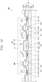
- FIG. 3 is a partial cross-sectional view of the display panel in correspondence to one pixel PX.
- the display panel DP includes a substrate SUB, a circuit element layer CL, a display element layer DPL, a thin-film encapsulation layer TFE, and a touch sensor TS. Although not shown, the display panel DP may further include a reflection protective layer and/or a window member, which are disposed on the touch sensor TS.
- the substrate SUB may include at least one plastic film.
- the substrate SUB may be flexible.
- the substrate SUB may include a plastic substrate, a glass substrate, a metal substrate, or an organic/inorganic composite substrate, for example.
- the display area DA and the non-display area NDA described with reference to FIG. 1 may be defined on the substrate SUB in the same manner.
- the circuit element layer CL may include the signal lines, the scan line GL, the data line DL, and the power line PL, which are described with reference to FIG. 2 . Also, the circuit element layer CL may include the first transistor T1, the second transistor T2, and the capacitor Cst. In FIG. 3 , the first transistor T1 is exemplarily described.
- the circuit element layer CL may include a barrier layer BR, an active layer ACT, a gate insulation film GI, a gate electrode GE, an interlayer insulation film ILD, input and output electrodes SE and DE, and an intermediate insulation layer VLD.
- the barrier layer BR is disposed on the substrate SUB and prevent foreign substances from being introduced through an upper portion of the barrier layer BR.
- the display panel DP may further include a buffer film (not shown) disposed on the barrier layer BR.
- the buffer film (not shown) increases a coupling force between the substrate SUB and layers disposed above the substrate SUB.
- the barrier layer BR and the buffer film (not shown) may be selectively provided or omitted.
- the active layer ACT is disposed on the barrier layer BR.
- the active layer ACT may serve as a channel area of the first transistor T1.
- the active layer ACT may include amorphous silicon, polysilicon, and a metal oxide semiconductor, for example.
- the gate insulation film GI may be disposed on the active layer ACT.
- the gate insulation film GI may insulate the gate electrode GE from the active layer ACT.
- the gate electrode GE may be disposed on the gate insulation film GI.
- the gate electrode GE may be disposed on the active layer ACT while overlapping the same.
- a first conductive layer (not shown) constituting signal lines may be disposed in the same layer as the gate electrode GE.
- the interlayer insulation film ILD is disposed on the gate electrode GE.
- the interlayer insulation film ILD electrically insulates the gate electrode GE and the input and output electrodes SE and DE from each other.
- the interlayer insulation film ILD may include an inorganic material.
- the inorganic material may include a silicon nitride, a silicon oxynitride, and a silicon oxide, for example.
- the input and output electrodes SE and DE are disposed on the interlayer insulation film ILD.
- the input and output electrodes SE and DE may be electrically connected to the active layer ACT through first and second contact holes CH1 and CH2 defined in the gate insulation film GI, respectively.
- a second conductive layer (not shown) constituting signal lines may be disposed in the same layer as the input and output electrodes SE and DE.
- the display panel DP exemplarily has a top-gate structure in which the gate electrode GE is disposed on the active layer ACT in an exemplary embodiment of the invention
- the display panel DP may have a bottom-gate structure in which the gate electrode GE is disposed below the active layer ACT in another exemplary embodiment.
- the interlayer insulation film ILD is disposed on the input and output electrodes SE and DE.
- the interlayer insulation film ILD may provide a planar surface.
- the interlayer insulation film ILD may include an organic material.
- the organic material may include at least one of an acryl-based resin, a methacryl-based resin, a polyisoprene-based resin, a vinyl-based resin, an epoxy-based resin, a urethane-based resin, a cellulose-based resin, a siloxane-based resin, a polyimide-based resin, a polyamide-based resin, and a perylene-based resin, for example.
- the display element layer DPL is disposed on the intermediate insulation layer VLD.
- the display element layer DPL may include a pixel defining film PDL and a display element.
- the display element may be the organic light emitting diode OLED.
- the organic light emitting diode OLED includes a first electrode AE, a hole control layer HCL, a light emitting layer EML, an electron control layer ECL, and a second electrode CE.
- the pixel defining layer PDL may include an organic material.
- the first electrode AE is disposed on the intermediate insulation layer VLD.
- the first electrode AE is connected to the output electrode DE through a third contact hole CH3 passing through the intermediate insulation layer VLD.
- a first opening OP1 is defined in the pixel defining film PDL.
- the first opening OP1 of the pixel defining film PDL exposes at least a portion of the first electrode AE.
- the pixel may be disposed on a pixel area in a plan view.
- the pixel area may include a light emitting area PXA and a non-light emitting area NPXA disposed adjacent to the light emitting area PXA.
- the non-light emitting area NPXA may surround the light emitting area PXA.
- the light emitting area PXA is defined in correspondence to a partial area of the first electrode AE, which is exposed by the first opening OP1.
- the hole control layer HCL may be disposed in the light emitting area PXA and the non-light emitting area NPXA in common. Although not separately shown, a common layer such as the hole control layer HCL may be provided in the plurality of pixels PX in common.
- the light emitting layer EML is disposed on the hole control layer HCL.
- the light emitting layer EML may be disposed in an area corresponding to the first opening OP1. That is, the light emitting layer EML may be separately provided in each of the plurality of pixels PX.
- the light emitting layer EML may include an organic material and/or an inorganic material.
- the patterned light emitting layer EML is exemplarily illustrated in this exemplary embodiment, the light emitting layer EML may be disposed in the plurality of pixels PX in common.
- the light emitting layer EML may generate white-color light, for example.
- the light emitting layer EML may have a multi-layer structure.
- the electron control layer ECL is disposed on the light emitting layer EML.
- a common layer such as the hole control layer HCL may be provided in the plurality of pixels PX in common.
- the second electrode CE is disposed on the electron control layer ECL.
- the second electrode CE is disposed in the plurality of pixels PX in common.
- the thin-film encapsulation layer TFE is disposed on the second electrode CE.
- the thin-film encapsulation layer TFE is disposed in the plurality of pixels PX in common.
- the thin-film encapsulation layer TFE directly covers the second electrode CE.
- a capping layer for covering the second electrode CE may be further disposed between the thin-film encapsulation layer TFE and the second electrode CE.
- the thin-film encapsulation layer TFE may directly cover the capping layer.
- the thin-film encapsulation layer TFE includes at least one inorganic film (hereinafter, referred to as an encapsulation inorganic film).
- the thin-film encapsulation layer TFE may further include at least one organic film (hereinafter, referred to as an encapsulation organic film).
- the encapsulation inorganic film protects the display element layer DPL from moisture/oxygen, and the encapsulation organic layer protects the display element layer DPL from foreign substances such as dust particles.
- the encapsulation inorganic film may include a silicon nitride layer, a silicon oxynitride layer, a silicon oxide layer, a titanium oxide layer, or an aluminum oxide layer, for example.
- the encapsulation organic film may include an acryl-based organic layer, the invention is not limited thereto.
- the touch sensor TS is disposed on the thin-film encapsulation layer TFE.
- the touch sensor TS acquires coordinate information of external input.
- the touch sensor TS is directly disposed on the thin-film encapsulation layer TFE.
- a wording of "directly disposed" represents formation through a continuous process instead of attachment by a separated adhesive layer.
- the touch sensor TS may detect an external input in a capacitance method, for example.
- the invention is not limited to the operation method of the touch sensor TS.
- the touch sensor TS according to an exemplary embodiment of the invention may detect an external input in an electromagnetic induction method or a pressure sensing method, for example.
- the touch sensor TS may have a multi-layer structure.
- the touch sensor TS may include a single-layer or multi-layer conductive layer.
- the touch sensor TS may include a single-layer or multi-layer insulation layer.
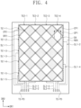
- FIG. 4 is a plan view of the touch sensor in FIG. 3
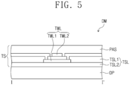
- FIG. 5 is a cross-sectional view taken along line I-I' in FIG. 4 .
- the touch sensor TS may include a touch electrode layer TML and a touch insulation layer TSL.
- the touch insulation layer TSL may contact the touch electrode layer TML.
- the touch electrode layer TML may include a first touch electrode layer TML1 and a second touch electrode layer TML2.
- the touch insulation layer TSL may include a first touch insulation layer TSL1 and a second touch insulation layer TSL2.
- the second touch electrode layer TML2 may be disposed on the first touch electrode layer TML1.
- Each of the first touch electrode layer TML1 and the second touch electrode layer TML2 may have a single-layer structure or a laminated multi-layer structure.
- the conductive layer having a multi-layer structure may include at least two or more layers of transparent layers and metal layers.
- the conductive layer having the multi-layer structure may include metal layers each of which includes different metal from each other.
- the transparent conductive layer may include an indium tin oxide ("ITO"), an indium zinc oxide (“IZO”), a zinc oxide (“ZnO”), an indium tin zinc oxide (“ITZO”), PEDOT, a metal nano-wire, and graphene, for example.
- the metal layer may include molybdenum, silver, titanium, copper, aluminum, and an alloy thereof, for example.
- each of the first touch electrode layer TML1 and the second touch electrode layer TML2 may have a three-layer structure of titanium/aluminum/titanium, for example.
- the first touch insulation layer TSL1 may be disposed between the first touch electrode layer TML1 and the second touch electrode layer TML2.
- the second touch insulation layer TSL2 may be disposed between the uppermost layer (thin-film encapsulation layer TFE (refer to FIG. 3 )) of the display panel DP and the first touch electrode layer TML1.
- the invention is not limited thereto.
- the second touch insulation layer TSL2 may be selectively omitted, for example.
- Each of the first touch insulation layer TSL1 and the second touch insulation layer TSL2 may include an inorganic material.
- the inorganic material may include a silicon nitride, a silicon oxynitride, and a silicon oxide, for example.
- the touch sensor TS may further include a planarization film PAS disposed on the second touch electrode layer TML2.
- the planarization film PAS may provide a planar surface and include an organic material.
- the touch sensor TS may include: first touch electrodes TE1-1 to TE1-5, first touch signal lines SL1-1 to SL1-5 connected to the first touch electrodes TE1-1 to TE1-5, second touch electrodes TE2-1 to TE2-4, second touch signal lines SL2-1 to SL2-4 connected to the second touch electrodes TE2-1 to TE2-4, and touch pads TS-PD connected to the first touch signal lines SL1-1 to SL1-5 and the second touch signal lines SL2-1 to SL2-4.
- Each of the first touch electrodes TE1-1 to TE1-5 may have a mesh shape in which a plurality of touch openings is defined.
- Each of the first touch electrodes TE1-1 to TE1-5 includes a plurality of first touch sensor parts SP1 and a plurality of first connecting parts CP1.
- the first touch sensor parts SP1 are disposed in the first direction DR1.
- Each of the first connecting parts CP1 connects two first touch sensor parts SP1 adjacent to each other among the first touch sensor parts SP1.
- the first touch signal lines SL1-1 to SL1-5 may also have the mesh shape.
- the second touch electrodes TE2-1 to TE2-4 cross the first touch electrodes TE1-1 to TE1-5 in an insulation manner.
- Each of the second touch electrodes TE2-1 to TE2-4 may have a mesh shape in which a plurality of touch openings is defined.
- Each of the second touch electrodes TE2-1 to TE2-4 includes a plurality of second touch sensor parts SP2 and a plurality of second connecting parts CP2.
- the second touch sensor parts SP2 are disposed in the second direction DR2.
- Each of the second connecting parts CP2 connects two second touch sensor parts SP2 adjacent to each other among the second touch sensor parts SP2.
- the second touch signal lines SL2-1 to SL2-4 may also have the mesh shape.
- the first touch electrodes TE1-1 to TE1-5 and the second touch electrodes TE2-1 to TE2-4 are capacitively coupled to each other. As touch sensing signals are applied to the first touch electrodes TE1-1 to TE1-5, capacitors are provided between the first touch sensor parts SP1 and the second touch sensor parts SP2.
- the plurality of first connecting parts CP1 is provided from the first touch electrode layer TML1, and the plurality of first touch sensor parts SP1 and the plurality of second connecting parts CP2 are provided from the second touch electrode layer TML2.
- a portion of the first touch sensor parts SP1, the plurality of first connecting parts CP1, the first touch signal lines SL1-1 to SL1-5, the second touch sensor parts SP2, the plurality of second connecting parts CP2, and the second touch signal lines SL2-1 to SL2-4 may be provided from the first touch electrode layer TML1 in FIG. 5 , and another portion thereof may be provided from the second touch electrode layer TML2 in FIG. 5 , for example.
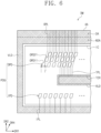
- FIG. 6 is an enlarged partial plan view illustrating area AA of the display apparatus DM in FIG. 1 not falling within the scope of the invention.
- the display panel DP may further include a pad group PDG disposed in the non-display area NDA and a test circuit TCR.
- the pad group PDG may include input pads IPD and output pads OPD.
- the output pads OPD are disposed relatively closer to the display area DA than the input pads IPD is to the display area DA.
- the driving circuit chip IC is electrically connected to the display panel DP through the input pads IPD and the output pads OPD.
- the display panel DP may further include output pad lines OPL and input pad lines IPL.
- the output pad lines OPL connect the output pads OPD to a portion (e.g., data lines DL) of the signal lines.
- the input pad lines IPL connect the input pads IPD to the flexible printed circuit board FPC.
- the driving circuit chip IC receives a signal provided from the flexible printed circuit board FPC through the input pad lines IPL and the input pads IPD.
- the driving circuit chip IC may provide a signal to at least a portion of the scan line GL, the data line DL, and the power line PL through the output pads OPD and the output pad lines OPL.
- the output pads OPD may be provided in a plurality of rows.
- the output pads OPD disposed in one row may be spaced apart from each other in the first direction DR1.
- the output pads OPD are exemplarily disposed in three rows in FIG. 6 , the number of rows is not limited thereto. In an exemplary embodiment, the output pads OPD may be disposed in two or less rows or four or more rows, for example.
- the input pads IPD are exemplarily provided in one row in FIG. 6 .
- the input pads IPD may be provided in a plurality of rows, for example.
- Each of the input pads IPD and the output pads OPD may have a short side and a long side. Each of the short sides of the input pads IPD and the output pads OPD may extend in the first direction DR1. Each of the long sides of the input pads IPD and the output pads OPD may extend in a fourth direction DR4 crossing the first and second directions DR1 and DR2.
- Pads which are disposed in rows corresponding to each other, of the plurality of output pads OPD disposed in rows different from each other may be spaced apart from each other in the fourth direction DR4.
- an output pad OPD11 disposed in a first row and a first column and an output pad OPD21 disposed in a second row and a first row may be spaced apart from each other in the fourth direction DR4, for example.
- the test circuit TCR may overlap the driving circuit chip IC in the non-display area NDA.
- the display panel DP may further include test pad lines TPL connecting the test circuit TCR to the output pads OPD.
- the test pad lines TPL may be connected to a predetermined number of the output pads OPD, e.g., the output pads OPD connected to the data line DL.
- the test circuit TCR provides a signal for testing an operation state of the display panel DP before released as a final product to the display panel DP through the test pad lines TPL and the output pads OPD.
- the test circuit TCR may be deactivated after product release.
- the test circuit TCR is provided to overlap the driving circuit chip IC instead of being provided in a partial area of the non-display area NDA that does not overlap the driving circuit chip IC. Accordingly, the non-display area NDA may be reduced in size, and thus, a space utilization rate may increase.
- the intermediate insulation layer VLD exposes the pad group PDG so that the pad group PDG and the driving circuit chip IC contact each other.
- the intermediate insulation layer VLD serves to protect the test circuit TCR by covering the test circuit TCR.
- a groove pattern is defined around the pad group PDG in the touch insulation layer TSL (refer to FIG. 5 ) in a plan view. Detailed description will be described later.
- FIG. 7 is a cross-sectional view taken along line I-I' of FIG. 6 .
- the cross-sectional structure of one output pad of the output pads OPD will be described with reference to FIG. 7 .
- the output pads OPD and the input pads IPD are substantially the same in structure as each other.
- the display panel DP includes a data pad pattern DPP contacting the output pad OPD and a gate pad pattern GPP.
- the gate pad pattern GPP is disposed in the same layer as the gate electrode GE in FIG. 3
- the data pad pattern DPP is disposed in the same layer as the input and output electrodes SE and DE in FIG. 3
- the output pad OPD is disposed in the same layer as one of the first touch electrode layer TML1 and the second touch electrode layer TML2 in FIG. 5 .
- the output pad OPD may be disposed in the same layer as the second touch electrode layer TML2.
- the data pad pattern DPP may be selectively omitted.
- the output pad lines OPL and the test pad lines TPL may be disposed in the same layer as the gate pad pattern GPP and electrically connected to the gate pad pattern GPP.
- a second opening OP2 exposing at least a portion of the gate pad pattern GPP is defined in the interlayer insulation film ILD, and the gate pad pattern GPP and the data pad pattern DPP contact each other through the second opening OP2.
- a third opening OP3 exposing at least a portion of the data pad pattern DPP is defined in the first touch insulation layer TSL1 and the second touch insulation layer TSL2, and the output pad OPD and the data pad pattern DPP contact each other through the third opening OP3.
- the first touch insulation layer TSL1 and the second touch insulation layer TSL2 include the substantially same material as each other, and the groove patterns having the same shape as each other are defined in the first touch insulation layer TSL1 and the second touch insulation layer TSL2. Accordingly, hereinafter, the first touch insulation layer TSL1 and the second touch insulation layer TSL2 will be described as a touch insulation layer TSL instead of being separately described.
- a wording that the groove pattern is defined in the touch insulation layer TSL represents that the recesses pattern is defined in each of the first touch insulation layer TSL1 and the second touch insulation layer TSL2, for example.
- FIG. 8 is a view illustrating a shape of a groove pattern GR according to an exemplary embodiment of the invention in an enlarged plan view of the area AA in FIG. 1
- FIG. 9 is a cross-sectional view taken along line II-II' in FIG. 8 .
- the output pads OPD may include central output pads OPDC and outer output pads OPDP.
- the outer output pads OPDP may be disposed outside the central output pads OPDC.
- outer output pads OPDP is disposed at one outside of the central output pads OPDC in the first direction DR1 in FIG. 8
- the outer output pads OPDP may be disposed at the other outside of the central output pads OPDC in the first direction DR1.
- a predetermined number of the outer output pads OPDP may not overlap the test circuit TCR in the second direction DR2.
- the central output pads OPDC may overlap the test circuit TCR in the second direction DR2.
- the output pads OPD are exemplarily disposed in three rows in an exemplary embodiment of the invention.
- the output pads OPD may be classified into first to third row output pads 101, 102, and 103 in an order adjacent to the test circuit TCR.
- outer output pads OPDP are exemplarily illustrated as output pads disposed from the first row that is the outermost row to the third row in FIG. 8 , the invention is not limited thereto. In an exemplary embodiment, the number of the outer output pads OPDP may be variously set, for example.
- the input pads IPD may include central input pads IPDC and outer input pads IPDP.
- the outer input pads IPDP may be disposed outside the central input pads IPDC.
- At least a predetermined number of the outer input pads IPDP may not overlap the test circuit TCR in the second direction DR2.
- the central input pads IPDC may overlap the test circuit TCR in the second direction DR2.
- outer input pads IPDP are exemplarily illustrated as input pads disposed from the first row that is the outermost row to the third row in FIG. 8 , the invention is not limited thereto. In an exemplary embodiment the number of the outer input pads IPDP may be variously set, for example.
- a groove pattern GR is defined in the touch insulation layer TSL.
- the groove pattern GR may be a hole passing through the touch insulation layer TSL.
- the invention is not limited thereto.
- the groove pattern GR may pass through the touch insulation layer TSL and define a groove in the interlayer insulation film ILD, for example.
- the groove pattern GR overlaps the non-display area NDA in the plan view.
- the groove pattern GR may overlap the driving circuit chip IC in the plan view.
- the groove pattern GR is disposed between the central output pads OPDC and the intermediate insulation layer VLD.
- a distance between the groove pattern GR and the central output pads OPDC may be shorter than that between the central output pads OPDC and the intermediate insulation layer VLD.
- the groove pattern GR may overlap at least a predetermined number of the central output pads OPDC.
- the groove pattern GR does not overlap at least a predetermined number of the outer output pads OPDP.
- the intermediate insulation layer VLD may include a first intermediate insulation layer VLD1 and a second intermediate insulation layer VLD2.
- the first intermediate insulation layer VLD1 and the second intermediate insulation layer VLD2 may be spaced apart from each other.
- the second intermediate insulation layer VLD2 may be disposed between the output pads OPD and the input pads IPD in the second direction DR2.
- the second intermediate insulation layer VLD2 may overlap the driving circuit chip IC (refer to FIG. 6 ) and cover the test circuit TCR (refer to FIG. 6 ).
- the first intermediate insulation layer VLD1 may be the remaining portion except for the second intermediate insulation layer VLD2.
- a fourth opening OP4 is defined in the first intermediate insulation layer VLD1, and the pad group PDG is exposed through the fourth opening OP4.
- the fourth opening OP4 may have a rectangular shape that is similar to a planar shape of the driving circuit chip IC.
- the fourth opening OP4 having the rectangular shape has first to fourth inside surfaces.
- a first inside surface IS1 adjacent to the display area DA and extending in the first direction DR1 a second inside surface IS2 in parallel to the first inside surface IS1, and a third inside surface IS3 connecting the first inside surface IS1 to the second inside surface IS2 are illustrated.
- a fourth inside surface (not shown) is not shown, the fourth inside surface may face the third inside surface IS3 and connect the first and second inside surfaces IS1 and IS2 to each other.
- the groove pattern GR may include first to fourth groove patterns GR1 to GR4.
- the first groove pattern GR1 may pass-through between the central output pads OPDC and the second intermediate insulation layer VLD2.
- the first groove pattern GR1 may have a linear shape extending in the first direction DR1.
- the first groove pattern GR1 may not overlap a predetermined number of the outer output pads OPDP in the second direction DR2.
- the first groove pattern GR1 exemplarily does not overlap all of the first row output pads 101, which are disposed in the first row, of the outer output pads OPDP in the second direction DR2.
- the first groove pattern GR1 may overlap all of the central output pads OPDC in the second direction DR2.
- the second groove pattern GR2 may pass-through between the central input pads IPDC and the second intermediate insulation layer VLD2.
- the second groove pattern GR2 may have a linear shape extending in the first direction DR1.
- the second groove pattern GR2 may not overlap a predetermined number of the outer input pads IPDP in the second direction DR2.
- the second groove pattern GR2 exemplarily dose not overlap all of the outer input pads IPDP in the second direction DR2.
- the second groove pattern GR2 may overlap all of the central input pads IPDC in the second direction DR2.
- the third groove pattern GR3 may pass-through between the central output pads OPDC and the first inside surface IS1 of the first intermediate insulation layer VLD1.
- the third groove pattern GR3 may have a linear shape extending in the first direction DR1.
- the third groove pattern GR3 may not overlap a predetermined number of the outer output pads OPDP in the second direction DR2.
- the third groove pattern GR3 exemplarily dose not overlap all of the outer output pads OPDP in the second direction DR2.
- the third groove pattern GR3 may overlap at least a predetermined number of the central output pads OPDC in the second direction DR2.
- the third groove pattern GR3 exemplarily overlaps all of the output pads 103, which are disposed in the third row, of the outer output pads OPDP in the second direction DR2.
- the fourth groove pattern GR4 may pass-through between the central input pads IPDC and the second inside surface IS2 of the first intermediate insulation layer VLD1.
- the fourth groove pattern GR4 may have a linear shape extending in the first direction DR1.
- the fourth groove pattern GR4 may not overlap a predetermined number of the outer output pads OPDP in the second direction DR2.
- the fourth groove pattern GR4 exemplarily dose not overlap all of the outer input pads IPDP in the second direction DR2.
- the fourth groove pattern GR4 may overlap at least a predetermined number of the central input pads IPDC in the second direction DR2.
- the interlayer insulation film ILD (refer to FIG. 9 ) may be exposed by the first to fourth groove patterns GR1 to GR4.
- first to fourth groove patterns GR1 to GR4 are exemplarily defined in the touch insulation layer TSL, the invention is not limited thereto.
- the first to fourth groove patterns GR1 to GR4 may extend to be defined in a portion of the interlayer insulation film ILD, for example.
- the display apparatus DM may further include a bump BMP.
- the bump BMP may be attached to one surface of the driving circuit chip IC, which faces the display panel DP.
- the bump BMP may include a conductive material.
- the driving circuit chip IC may receive a voltage and current signal through the bump BMP.
- the driving circuit chip IC may be disposed (e.g., mounted) in such a manner that an anisotropic conductive film ("ACF") is disposed between the driving circuit chip IC and the display panel DP and then thermally compressed at a high temperature.
- ACF anisotropic conductive film
- the ACF may include a plurality of conductive balls 150 and an adhesive material 151.
- the conductive ball 150 may allow the bump BMP and the input and output pads IPD and OPD to be electrically connected to each other.
- the output pad OPD contacts an output data pad pattern DPP1 through a fifth opening OPS defined in the touch insulation layer TSL, and the output data pad pattern DPP1 contacts an output gate pad pattern GPP1 through a sixth opening OP6 defined in the interlayer insulation film ILD.
- the input pad IPD contacts an input data pad pattern DPP2 through a seventh opening OP7 defined in the touch insulation layer TSL, and the input data pad pattern DPP2 contacts an input gate pad pattern GPP2 through a eighth opening OP8 defined in the interlayer insulation film ILD.
- the test circuit TCR may include at least one of a first test pattern TCR1 and a second test pattern TCR2.
- the first test pattern TCR1 may be disposed in the same layer as the output gate pad pattern GPP1 and the input gate pad pattern GPP2.
- the second test pattern TCR2 may be disposed in the same layer as the output data pad pattern DPP1 and the input data pad pattern DPP2.
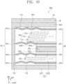
- FIG. 10 is a view exemplarily illustrating a cross-section of a display apparatus corresponding to a comparative example
- FIG. 11 is a photograph showing the cross-section of the display apparatus corresponding to the comparative example
- FIG. 12 is a photograph showing a defect occurred in a mobile terminal to which the display apparatus corresponding to the comparative example is applied.
- FIG. 10 has the substantially same structure as that in FIG. 9 except for the groove pattern GR in FIG. 9 .
- FIG. 10 is a cross-sectional view taken along line III-III' of FIG. 8 .
- a component, which corresponds to that of the display apparatus in FIG. 9 , of components in FIG. 10 is indicated by adding "-1" to the reference symbol of the corresponding component of the display apparatus in FIG. 9 .
- each of an interlayer insulation film ILD-1 and a touch insulation layer TSL-1 includes an inorganic material, each of an interlayer insulation film ILD-1 and a touch insulation layer TSL-1 has a relatively weak coupling force. Accordingly, the touch insulation layer TSL-1 and the interlayer insulation film ILD-1 are easily delaminated from each other.
- a crack CRK may be generated in the touch insulation layer TSL-1.
- the crack CRK may be generated due to various reasons. While a process of compressing a driving circuit chip IC-1 is preformed, a conductive ball 150-1 may apply a pressure to the touch insulation layer TSL-1 to generate the crack CRK in the touch insulation layer TSL-1, for example. Also, as the flexible display panel DP (refer to FIG. 9 ) is bent, the touch insulation layer TSL-1 may be also bent to generate the crack CRK therein.
- FIG. 11 shows that the touch insulation layer TSL-1 and the interlayer insulation film ILD-1 are delaminated by a first distance DT.
- a fluid path PTH through which moisture may pass between the touch insulation layer TSL-1 and the interlayer insulation film ILD-1 may be defined, and, as the moisture moves through the fluid path PTH, pads adjacent to each other may be short-circuited.
- the output pads OPD adjacent to each other may be short-circuited through the fluid path PTH.
- two adjacent output pads OPD-1 are exemplarily short-circuited.
- the display apparatus DM-1 corresponding to the comparative example may have various kinds of defects according to a combination of the input and output pads IPD and OPD in addition to the defect having a vertical line shape in FIG. 12 .
- the display apparatus DM may fundamentally prevent a delamination phenomenon between the touch insulation layer TSL and the interlayer insulation film ILD or prevent the delamination phenomenon generated between the touch insulation layer TSL and the interlayer insulation film ILD from being transferred to the input pad IPD and the output pad OPD.
- the intermediate insulation layer VLD has a thickness relatively greater than that of layers disposed therebelow except for the substrate SUB.
- the intermediate insulation layer VLD may have a thickness equal to or greater than about 10000 angstroms ( ⁇ )
- each of the barrier layer BR, the active layer ACT, the gate insulation layer GI, the gate electrode GE, the interlayer insulation film ILD, and the input and output electrodes SE and DE may have a thickness equal to or less than about 10000 ⁇ , for example.
- the intermediate insulation layer VLD has a relatively thick thickness and the touch insulation layer TSL has a relatively thin thickness
- the touch insulation layer TSL overlapping the first to third inside surfaces IS1 to IS3 and the fourth inside surface (not shown) is relatively vulnerable to the crack.
- the crack may be generated in the touch insulation layer TSL overlapping the driving circuit chip IC due to the pressure of the conductive ball 150 during the compression process of the driving circuit chip IC. That is, there is a high possibility that the crack is generated in the touch insulation layer TSL at a position in which the touch insulation layer TSL overlaps the intermediate insulation layer VLD.
- the groove pattern GR is defined in a position overlapping the intermediate insulation layer VLD to prevent the delamination phenomenon between the touch insulation layer TSL and the interlayer insulation film ILD due to the crack generated in the touch insulation layer TSL from being transferred to the output pads OPD and the input pads IPD.
- the short-circuit caused by the delamination phenomenon between the touch insulation layer TSL and the interlayer insulation film ILD may be prevented from being generated between the output pads OPD and the input pads IPD.
- the pads are disposed on both sides of each of the central output pads OPDC and the central input pads IPDC in the first direction DR1, the stress applied to the central output pads OPDC and the central input pads IPDC when the driving circuit chip IC is disposed (e.g., mounted) on the display panel DP may be distributed.
- the outer output pads OPDP and the outer input pads IPDP since the pads are disposed at only one side in the first direction DR1, a stress is concentrated thereon in comparison with the central output pads OPDC and the central input pads IPDC.
- the crack may be generated over the entire display panel along the groove pattern.
- the crack may be generated along the groove pattern in the process of mounting the driving circuit chip IC to generate a defect of the display apparatus.
- the delamination limitation between the touch insulation layer TSL and the interlayer insulation film ILD may be solved, and, at the same time, as the groove pattern does not overlap at least a predetermined number of the outer output pads OPDP and at least a predetermined number of the outer input pads IPDP in the second direction DR2 to allow the stress to be concentrate on the area in which outer output pads OPDP and the outer input pads IPDP are disposed, the limitation in which the crack is generated in the display panel may be solved.
- FIG. 13 is a view illustrating a shape of a groove pattern according to another exemplary embodiment of the invention in an enlarged plan view of the area AA in FIG. 1
- FIG. 14 is a cross-sectional view taken along line II-II' in FIG. 13 .
- a display apparatus DM1 which will be described with reference to FIGS. 13 and 14 , according to another exemplary embodiment of the invention includes the substantially same components as those of the display apparatus DM, which has been described with reference to FIGS. 8 and 9 , according to an exemplary embodiment of the invention, except for a shape of a groove pattern GR-1.
- the shape of the groove pattern GR-1 will be described in detail, and components that are not described will follow the description of FIGS. 8 and 9 .
- the groove pattern GR-1 may further include a fifth groove pattern GR5.
- the fifth groove pattern GR5 is disposed between the first and second groove patterns GR1 and GR2 and spaced apart from the first and second groove patterns GR1 and GR2 in the second direction DR2.
- the fifth groove pattern GR5 exposes the second intermediate insulation layer VLD2 and the interlayer insulation film ILD. That is, the touch insulation layer TSL does not overlap the second intermediate insulation layer VLD2.
- the fifth groove pattern GR5 fundamentally prevent a crack from being generated around the second intermediate insulation layer VLD2.
- FIG. 15 is a view illustrating a shape of a groove pattern according to an example not being part of the invention in an enlarged plan view of the area AA in FIG. 1 .
- a display apparatus DM2 which will be described with reference to FIG. 15 , includes the substantially same components as those of the display apparatus DM, which has been described with reference to FIGS. 8 and 9 , according to an exemplary embodiment of the invention, except for an outer groove pattern PR.
- the groove pattern PR will be described in detail, and components that are not described will follow the description of FIGS. 8 and 9 .
- the outer groove pattern PR may be further defined in the touch insulation layer TSL (refer to FIG. 9 ).
- the outer groove pattern PR may include a plurality of holes disposed in parallel in a specific direction.
- the plurality of holes may pass through the touch insulation layer TSL and define a groove in the interlayer insulation film ILD after passing through the touch insulation layer TSL.
- the plurality of holes may have the substantially the same cross-sectional shape (depth) as that of the groove pattern GR.
- the outer groove pattern PR may include first to fourth outer groove patterns PR1 to PR4.
- the first to fourth outer groove patterns PR1 to PR4 may be disposed adjacent to the first to fourth groove patterns GR1 to GR4 in the first direction DR1, respectively.
- Each of the first to fourth outer groove patterns PR1 to PR4 may include a plurality of holes that spaced apart from each other in the first direction DR1.
- the first to fourth outer groove patterns PR1 to PR4 may overlap the outer output pads OPDP and the outer input pads IPDP in the second direction DR2.
- the delamination limitation between the touch insulation layer TSL (refer to FIG. 9 ) and the interlayer insulation film ILD (refer to FIG. 9 ) may be solved, and, at the same time, as the stress applied to an area, in which the outer output pads OPDP and the outer input pads IPDP are disposed, is distributed, the limitation of crack occurrence in the display panel may be solved.
- FIG. 16 is a view illustrating a shape of a groove pattern according to another example not being part of the invention in an enlarged plan view of the area AA in FIG. 1 .
- a display apparatus DM3 which will be described with reference to FIG. 16 , includes the substantially same components as those of the display apparatus DM, which has been described with reference to FIGS. 8 and 9 , according to an exemplary embodiment of the invention, except for an outer groove pattern PR-1.
- the groove pattern PR-1 will be described in detail, and components that are not described will follow the description of FIGS. 8 and 9 .
- the outer groove pattern PR-1 may be further defined in the touch insulation layer TSL (refer to FIG. 9 ).
- the outer groove pattern PR-1 may has a shape extending in a zig-zag manner along the first direction DR1.
- the outer groove pattern PR-1 may pass through the touch insulation layer TSL and define a groove in the interlayer insulation film ILD (refer to FIG. 9 ).
- the plurality of holes may have the substantially the same cross-sectional shape (depth) as that of the groove pattern GR.
- the outer groove pattern PR-1 may include first to fourth outer groove patterns PR11 to PR14.
- the first to fourth outer groove patterns PR11 to PR14 may be disposed adjacent to the first to fourth groove patterns GR1 to GR4 in the first direction DR1, respectively.
- the first to fourth outer groove patterns PR11 to PR14 are exemplarily connected to the first to fourth groove patterns GR1 to GR4, respectively, the invention is not limited thereto.
- the first to fourth outer groove patterns PR11 to PR14 may be spaced apart from the first to fourth groove patterns GR1 to GR4, respectively, in the first direction DR1, for example.
- Each of the first to fourth outer groove patterns PR11 to PR14 may have a shape in which linear patterns extending direction different from each other are connected to each other. However, the invention is not limited thereto. In an exemplary embodiment, each of the first to fourth outer groove patterns PR11 to PR14 may have a shape in which curved patterns are connected to each other, for example.
- the delamination limitation between the touch insulation layer TSL and the interlayer insulation film ILD may be solved, and, at the same time, as the stress applied to the area, in which the outer output pads OPDP and the outer input pads IPDP are disposed, is distributed, the limitation of crack occurrence in the display panel may be solved.
- FIG. 17 is a view illustrating a shape of a groove pattern according to another example not being part of the invention in an enlarged plan view of the area AA in FIG. 1 .
- a display apparatus DM4 which will be described with reference to FIG. 17 , includes the substantially same components as those of the display apparatus DM, which has been described with reference to FIGS. 8 and 9 , according to an exemplary embodiment of the invention, except for an outer groove pattern PR-2.
- the groove pattern PR-2 will be described in detail, and components that are not described will follow the description of FIGS. 8 and 9 .
- the outer groove pattern PR-2 may be further defined in the touch insulation layer TSL (refer to FIG. 9 ).
- the outer groove pattern PR-2 may include first to eighth outer groove patterns PR21 to PR28. Each of the first to eighth outer groove patterns PR21 to PR28 may be provided in plurality.
- the first and second outer groove patterns PR21 to PR22 may be disposed between the second intermediate insulation layer VLD2 and the outer output pads OPDP.
- the first and second outer groove patterns PR21 and PR22 may overlap the outer output pads OPDP in the second direction DR2.
- the first outer groove patterns PR21 may be spaced apart from each other in the first direction DR1.
- the second outer groove patterns PR22 may be spaced apart from each other in the first direction DR1.
- the first and second outer groove patterns PR21 and PR22 may have different distances spaced from the output pads disposed in any one row in the second direction DR2. With reference to the output pads OPD disposed in the first row, the first outer groove patterns PR21 may be spaced by a first distance TT1, and the second outer groove patterns PR22 may be spaced by a second distance TT2.
- the first outer groove patterns PR21 may be disposed between the second outer groove patterns PR22 in the first direction DR1.
- the third and fourth outer groove patterns PR23 and PR24 may be disposed between the second intermediate insulation layer VLD2 and the outer input pads IPDP.
- the third and fourth outer groove patterns PR23 and PR24 may overlap the outer input pads IPDP in the second direction DR2.
- the third outer groove patterns PR23 may be spaced apart from each other in the first direction DR1
- the fourth outer groove patterns PR24 may be spaced apart from each other in the first direction DR1.
- the third and fourth outer groove patterns PR23 and PR24 may have different distances spaced from the input pads IPD disposed in any one row in the second direction DR2.
- the third outer groove patterns PR23 may be disposed between the fourth outer groove patterns PR24 in the first direction DR1.
- the fifth and sixth outer groove patterns PR25 and PR26 may be disposed between the outer output pads OPDP and the first inside surface IS1 of the first intermediate insulation layer VLD1.
- the fifth and sixth outer groove patterns PR25 and PR26 may overlap the outer output pads OPDP in the second direction DR2.
- the fifth outer groove patterns PR25 may be spaced apart from each other in the first direction DR1
- the sixth outer groove patterns PR26 may be spaced apart from each other in the first direction DR1.
- the fifth and sixth outer groove patterns PR25 and PR26 may have different distances spaced from the output pads disposed in any one row in the second direction DR2.
- the fifth outer groove patterns PR25 may be between the sixth outer groove patterns PR26 in the first direction DR1.
- the seventh and eighth outer groove patterns PR27 and PR28 may be disposed between the outer input pads IPDP and the second inside surface IS2 of the first intermediate insulation layer VLD1.
- the seventh and eighth outer groove patterns PR27 and PR28 may overlap the outer input pads IPDP in the second direction DR2.
- the seventh outer groove patterns PR27 may be spaced apart from each other in the first direction DR1
- the eighth outer groove patterns PR28 may be spaced apart from each other in the first direction DR1.
- the seventh and eighth outer groove patterns PR27 and PR28 may have different distances spaced from the output pads disposed in any one row in the second direction DR2.
- the seventh outer groove patterns PR27 may be disposed between the eighth outer groove patterns PR28 in the first direction DR1.
- the delamination limitation between the touch insulation layer TSL and the interlayer insulation film ILD may be solved, and, at the same time, as the stress applied to the area, in which the outer output pads OPDP and the outer input pads IPDP are disposed, is distributed, the limitation of crack occurrence in the display panel may be solved.
- FIG. 18 is a view illustrating a shape of a groove pattern according to another example not being part of the invention in an enlarged plan view of the area AA in FIG. 1
- FIG. 19 is a cross-sectional view taken along line II-II' in FIG. 18 .
- a display apparatus DM5 which will be described with reference to FIGS. 18 and 19 , includes the substantially same components as those of the display apparatus DM, which has been described with reference to FIGS. 8 and 9 , according to an exemplary embodiment of the invention, except for a shape of a groove pattern GR-2 and a compensation pattern CP.
- a shape of a groove pattern GR-2 and a compensation pattern CP will be described in detail, and components that are not described will follow the description of FIGS. 8 and 9 .
- the groove pattern GR-2 may include first to fourth groove patterns GR11 to GR14.
- Each of the first to fourth groove patterns GR11 to GR14 in FIG. 18 may have a shape in which each of the groove patterns GR1 to GR4 in FIG. 8 further extends.
- each of the first to fourth groove patterns GR11 to GR14 may extend to the outer output pads OPDP and the outer input pads IPDP in the first direction DR1 and overlap the outer output pads OPDP and the outer input pads IPDP in the second direction DR2.
- the display panel DP-1 may further include the compensation pattern CP.
- the compensation pattern CP may be disposed on the touch insulation layer TSL.
- the compensation pattern CP may include first to fourth compensation patterns CP1 to CP4.
- the first to fourth compensation patterns CP1 to CP4 may overlap the first to fourth groove patterns GR11 to GR14, respectively.
- the first to fourth compensation patterns CP1 to CP4 may prevent the interlayer insulation film ILD from being exposed by the first to fourth groove patterns GR11 to GR14, respectively.
- the first to fourth compensation patterns CP1 to CP4 may overlap the outer output pads OPDP and the outer input pads IPDP in the second direction DR2.
- Each of the first to fourth compensation patterns CP1 to CP4 may include the same material as that of the touch insulation layer TSL.
- Partial areas of the first to fourth groove patterns GR11 to GR14 overlapping the outer output pads OPDP and the outer input pads IPDP in the second direction DR2 are covered by the first to fourth compensation patterns CP1 to CP4, respectively.
- the compensation pattern overlapping the groove patterns in the area overlapping the outer output pads OPDP and the outer input pads IPDP in the second direction DR2 are defined, the limitation, in which the crack is generated in the display panel because the stress is concentrated on the area in which the outer output pads OPDP and the outer input pads IPDP are disposed, may be solved.
- the short-circuit between the output pads and the input pads caused by the delamination phenomenon between the touch insulation layer and the interlayer insulation film is prevented by defining the groove pattern in the touch insulation layer.
- the crack generated due to the stress concentrated around the pads disposed at the outer portion of the display panel when the driving circuit chip is disposed (e.g., mounted) on the display panel may be prevented from being generated in the display panel.
Landscapes
- Engineering & Computer Science (AREA)
- Physics & Mathematics (AREA)
- Theoretical Computer Science (AREA)
- General Physics & Mathematics (AREA)
- General Engineering & Computer Science (AREA)
- Microelectronics & Electronic Packaging (AREA)
- Human Computer Interaction (AREA)
- Nonlinear Science (AREA)
- Computer Hardware Design (AREA)
- Mathematical Physics (AREA)
- Chemical & Material Sciences (AREA)
- Crystallography & Structural Chemistry (AREA)
- Optics & Photonics (AREA)
- Devices For Indicating Variable Information By Combining Individual Elements (AREA)
- Electroluminescent Light Sources (AREA)
Claims (10)
- Appareil d'affichage (DM) comprenant :un substrat (SUB) comprenant une zone d'affichage (DA) et une zone de non-affichage (NDA) disposée à l'extérieur de la zone d'affichage (DA) ;des lignes de signal disposées sur le substrat (SUB) ;une couche d'éléments d'affichage (DPL) disposée sur les lignes de signal et comprenant des éléments d'affichage disposés dans la zone d'affichage (DA) ; etun groupe de plots (PDG) connecté électriquement aux lignes de signal et comprenant des plots de sortie (OPD) disposés dans la zone de non-affichage (NDA)caractérisé parune couche d'isolation intermédiaire (VLD) disposée entre les lignes de signal et la couche d'éléments d'affichage (DPL) et exposant les plots de sortie (OPD) ;une couche d'électrode tactile (TML) disposée sur la couche d'éléments d'affichage (DPL) ; etune couche d'isolation tactile (TSL) disposée sur la couche d'éléments d'affichage (DPL), en contact avec la couche d'électrode tactile (TML), et dans laquelle un motif de rainure (GR) est défini dans la zone de non-affichage (NDA),dans lequel les plots de sortie (OPD) comprennent des plots de sortie centraux (OPDC) et des plots de sortie externes (OPDP) disposés à l'extérieur des plots de sortie centraux (OPDC) dans une première direction (DR1) ; etle motif de rainure (GR) est disposé entre les plots de sortie (OPD) et la couche d'isolation intermédiaire (VLD) et ne chevauche pas au moins un nombre prédéterminé des plots de sortie externes (OPDP) dans une seconde direction (DR2) croisant la première direction (DR1) dans une vue en plan.
- Appareil d'affichage (DM) selon la revendication 1, dans lequel les lignes de signal comprennent une première couche conductrice et une seconde couche conductrice disposée sur la première couche conductrice,l'appareil d'affichage (DM) comprend en outre un film d'isolation intercouche (ILD) disposé entre la première couche conductrice et la seconde couche conductrice, etchacun du film d'isolation intercouche (ILD) et de la couche d'isolation tactile (TSL) comprend un matériau inorganique.
- Appareil d'affichage (DM) selon au moins l'une des revendications 1 ou 2, dans lequel la couche d'isolation tactile (TSL) et le film d'isolation intercouche (ILD) sont en contact l'un avec l'autre dans au moins une zone partielle, et le motif de rainure (GR) expose le film d'isolation intercouche (ILD).
- Appareil d'affichage (DM) selon au moins l'une des revendications 1 à 3, dans lequel le groupe de plots (PDG) comprend en outre des plots d'entrée (IPD) disposés dans la zone de non-affichage (NDA) et espacés des plots de sortie (OPD) dans la seconde direction (DR2) dans la vue en plan,les plots d'entrée (IPD) comprennent des plots d'entrée centraux et des plots d'entrée externes disposés à l'extérieur des plots d'entrée centraux dans la première direction (DR1), etle motif de rainure (GR) est disposé entre les plots d'entrée (IPD) et le film d'isolation intercouche (ILD) et ne chevauche pas au moins un nombre prédéterminé des plots d'entrée externes dans la seconde direction (DR2) dans la vue en plan.
- Appareil d'affichage (DM) selon la revendication 4, comprenant en outre une puce de circuit de pilotage (IC) qui est électriquement connectée aux plots de sortie (OPD) et aux plots d'entrée (IPD) et fournit un signal aux lignes de signal ; et
un circuit chevauchant la puce de circuit de pilotage (IC) et connecté électriquement à au moins un nombre prédéterminé des plots de sortie (OPD). - Appareil d'affichage (DM) selon au moins l'une des revendications 1 à 5, dans lequel les plots de sortie centraux (OPDC) et les plots d'entrée centraux (OPCD) chevauchent le circuit dans la seconde direction (DR2) dans la vue en plan, et au moins un nombre prédéterminé des plots de sortie externes (OPDP) et au moins un nombre prédéterminé des plots d'entrée externes (OPCD) chevauchent le circuit dans la seconde direction (DR2) dans la vue en plan.
- Appareil d'affichage (DM) selon au moins l'une des revendications 1 à 6, dans lequel la couche d'isolation intermédiaire (VLD) comprend une première couche d'isolation intermédiaire (VLD1) dans laquelle une ouverture exposant le groupe de plots (PDG) est définie et une seconde couche d'isolation intermédiaire (VLD2) espacée de la première couche d'isolation intermédiaire (VLD1) et recouvrant le circuit dans la vue en plan.
- Appareil d'affichage (DM) selon la revendication 7, dans lequel le motif de rainure (GR) comprend un premier motif de rainure (GR1) traversant entre les plots de sortie centraux (OPDC) et la seconde couche d'isolation intermédiaire (VLD2) et ne chevauchant pas un nombre prédéterminé des plots de sortie externes (OPDP) dans la seconde direction (DR2).
- Appareil d'affichage (DM) selon au moins l'une des revendications 1 à 8, dans lequel le motif de rainure (GR) comprend en outre un deuxième motif de rainure (GR2) disposé entre les plots de sortie centraux (OPDC) et une surface latérale de l'ouverture de la première couche d'isolation intermédiaire (VLD1) adjacente à la zone d'affichage (DA) et ne chevauchant pas un nombre prédéterminé des plots de sortie externes (OPDP) dans la seconde direction (DR2).
- Appareil d'affichage (DM) selon au moins l'une des revendications 1 à 9, dans lequel le motif de rainure (GR) comprend en outre un troisième motif de rainure (GR3) exposant la seconde couche d'isolation intermédiaire (VLD2) et espacé du premier motif de rainure (GR1) dans la seconde direction (DR2).
Applications Claiming Priority (1)
| Application Number | Priority Date | Filing Date | Title |
|---|---|---|---|
| KR1020170163539A KR102503732B1 (ko) | 2017-11-30 | 2017-11-30 | 표시 장치 |
Publications (2)
| Publication Number | Publication Date |
|---|---|
| EP3496149A1 EP3496149A1 (fr) | 2019-06-12 |
| EP3496149B1 true EP3496149B1 (fr) | 2024-05-08 |
Family
ID=64572098
Family Applications (1)
| Application Number | Title | Priority Date | Filing Date |
|---|---|---|---|
| EP18209090.2A Active EP3496149B1 (fr) | 2017-11-30 | 2018-11-29 | Afficheur |
Country Status (4)
| Country | Link |
|---|---|
| US (4) | US10739892B2 (fr) |
| EP (1) | EP3496149B1 (fr) |
| KR (1) | KR102503732B1 (fr) |
| CN (2) | CN117784967A (fr) |
Families Citing this family (37)
| Publication number | Priority date | Publication date | Assignee | Title |
|---|---|---|---|---|
| US11189605B2 (en) * | 2018-02-28 | 2021-11-30 | X Display Company Technology Limited | Displays with transparent bezels |
| US10690920B2 (en) | 2018-02-28 | 2020-06-23 | X Display Company Technology Limited | Displays with transparent bezels |
| KR102569929B1 (ko) * | 2018-07-02 | 2023-08-24 | 삼성디스플레이 주식회사 | 디스플레이 장치 |
| US12236825B2 (en) | 2018-08-13 | 2025-02-25 | X Display Company Technology Limited | Redundant pixel layouts |
| KR102573704B1 (ko) | 2018-09-06 | 2023-09-04 | 삼성디스플레이 주식회사 | 만입된 형상의 표시부를 포함하는 표시 장치 |
| CN109168250B (zh) * | 2018-10-24 | 2020-04-17 | 合肥鑫晟光电科技有限公司 | 一种电路板及其制作方法、使用方法、显示装置 |
| CN109407434B (zh) * | 2018-11-22 | 2020-11-24 | 武汉华星光电技术有限公司 | 液晶显示装置 |
| KR102626707B1 (ko) * | 2018-12-27 | 2024-01-17 | 엘지디스플레이 주식회사 | 표시장치 |
| KR102628847B1 (ko) * | 2019-06-12 | 2024-01-25 | 삼성디스플레이 주식회사 | 디스플레이 장치 |
| US20220320457A1 (en) * | 2019-07-12 | 2022-10-06 | Sharp Kabushiki Kaisha | Display device |
| KR20210011529A (ko) * | 2019-07-22 | 2021-02-02 | 삼성디스플레이 주식회사 | 표시 장치 및 표시 장치의 제조 방법 |
| CN110416266B (zh) * | 2019-07-29 | 2022-07-22 | 京东方科技集团股份有限公司 | 显示基板及包含其的显示面板 |
| KR102939768B1 (ko) | 2019-09-25 | 2026-03-16 | 삼성디스플레이 주식회사 | 표시 장치 |
| KR102810632B1 (ko) * | 2019-10-14 | 2025-05-23 | 삼성디스플레이 주식회사 | 회로기판의 제조 방법 및 이를 포함한 표시장치 |
| US11232755B2 (en) * | 2019-10-23 | 2022-01-25 | Chengdu Boe Optoelectronics Technology Co., Ltd. | Display substrate and manufacturing method therefor, and display device |
| CN113099731B (zh) * | 2019-10-23 | 2024-10-22 | 京东方科技集团股份有限公司 | 显示基板及其制备方法、显示装置 |
| CN111383554B (zh) * | 2019-11-06 | 2021-12-17 | 上海中航光电子有限公司 | 显示面板及显示装置 |
| CN110689847B (zh) * | 2019-11-12 | 2021-03-05 | 京东方科技集团股份有限公司 | 显示面板、显示装置 |
| KR20210065580A (ko) | 2019-11-27 | 2021-06-04 | 엘지디스플레이 주식회사 | 플렉서블 표시장치 |
| KR102881054B1 (ko) * | 2019-12-04 | 2025-11-05 | 삼성디스플레이 주식회사 | 입력 감지 유닛 및 이를 포함한 표시장치 |
| KR102874148B1 (ko) * | 2019-12-30 | 2025-10-20 | 엘지디스플레이 주식회사 | 폴더블 표시 장치 |
| CN111142712B (zh) * | 2019-12-31 | 2023-07-18 | 信利(惠州)智能显示有限公司 | 柔性线路板、显示模组及显示屏 |
| US12262601B2 (en) * | 2020-04-21 | 2025-03-25 | Samsung Display Co., Ltd. | Light emitting display device and manufacturing method thereof |
| KR102744149B1 (ko) * | 2020-05-04 | 2024-12-20 | 삼성디스플레이 주식회사 | 게이트 검사부 및 이를 포함하는 표시 장치 |
| US11636786B2 (en) * | 2020-06-03 | 2023-04-25 | Samsung Display Co., Ltd. | Display device |
| CN113759618B (zh) * | 2020-06-04 | 2025-07-15 | 三星显示有限公司 | 显示装置 |
| CN111650793B (zh) * | 2020-06-28 | 2023-08-01 | 上海中航光电子有限公司 | 显示面板及其阵列基板 |
| KR20220006670A (ko) * | 2020-07-08 | 2022-01-18 | 삼성디스플레이 주식회사 | 표시 장치 |
| KR102899241B1 (ko) | 2020-07-31 | 2025-12-11 | 삼성디스플레이 주식회사 | 디스플레이 장치 |
| US12219831B2 (en) * | 2020-10-14 | 2025-02-04 | Samsung Display Co., Ltd. | Display apparatus |
| CN112259582B (zh) * | 2020-10-15 | 2023-01-24 | 武汉华星光电半导体显示技术有限公司 | 柔性显示面板及电子设备 |
| US11978743B2 (en) * | 2020-12-01 | 2024-05-07 | Everdisplay Optronics (Shanghai) Co., Ltd | TFT array substrate and display panel including the same |
| KR20220083938A (ko) * | 2020-12-11 | 2022-06-21 | 삼성디스플레이 주식회사 | 표시 장치 |
| US12238987B2 (en) | 2021-04-05 | 2025-02-25 | Samsung Display Co., Ltd. | Display device |
| KR20220140075A (ko) * | 2021-04-08 | 2022-10-18 | 삼성디스플레이 주식회사 | 입력 감지 장치 및 이를 포함하는 표시 장치 |
| US12216849B2 (en) | 2021-12-23 | 2025-02-04 | Chengdu Boe Optoelectronics Technology Co., Ltd. | Display panel and display apparatus having crack detection circuit with conductive loop |
| CN115663085B (zh) * | 2022-10-10 | 2026-04-03 | Tcl华星光电技术有限公司 | 基板及发光板 |
Family Cites Families (18)
| Publication number | Priority date | Publication date | Assignee | Title |
|---|---|---|---|---|
| KR100895311B1 (ko) | 2002-11-19 | 2009-05-07 | 삼성전자주식회사 | 액정 표시 장치 및 그 검사 방법 |
| KR100943730B1 (ko) | 2003-06-27 | 2010-02-23 | 엘지디스플레이 주식회사 | 씨오지 방식 디스플레이 장치 |
| JP5032187B2 (ja) * | 2007-04-17 | 2012-09-26 | 新光電気工業株式会社 | 配線基板の製造方法及び半導体装置の製造方法及び配線基板 |
| KR101427135B1 (ko) | 2008-10-14 | 2014-08-07 | 엘지디스플레이 주식회사 | 씨오지 타입 액정표시장치용 어레이 기판 |
| KR20130013515A (ko) | 2011-07-28 | 2013-02-06 | 삼성디스플레이 주식회사 | 유기 발광 표시 장치 |
| JP5812895B2 (ja) * | 2012-02-28 | 2015-11-17 | 株式会社ジャパンディスプレイ | 近接検出装置、近接検出方法、電子機器 |
| CN103576998B (zh) * | 2012-07-20 | 2017-07-28 | 上海思立微电子科技有限公司 | 电容式触摸屏及单层布线电极阵列 |
| KR101341030B1 (ko) | 2012-08-29 | 2013-12-13 | 엘지디스플레이 주식회사 | 유기 발광 표시 장치 및 이의 제조 방법 |
| KR102010492B1 (ko) | 2013-01-31 | 2019-08-13 | 엘지디스플레이 주식회사 | 액정표시장치 및 그의 제조방법 |
| US9472507B2 (en) * | 2013-06-17 | 2016-10-18 | Samsung Display Co., Ltd. | Array substrate and organic light-emitting display including the same |
| KR102257119B1 (ko) * | 2013-06-17 | 2021-05-31 | 삼성디스플레이 주식회사 | 어레이 기판 및 이를 포함하는 유기 발광 표시 장치 |
| KR20150080825A (ko) * | 2014-01-02 | 2015-07-10 | 삼성디스플레이 주식회사 | 표시 패널, 이를 포함하는 표시 장치 및 이의 제조 방법 |
| US9666814B2 (en) * | 2014-03-07 | 2017-05-30 | Samsung Display Co., Ltd. | Display device and method of manufacturing the same |
| KR102334547B1 (ko) | 2014-06-17 | 2021-12-03 | 삼성디스플레이 주식회사 | 어레이 기판 및 이를 이용한 집적 회로 실장 방법 |
| KR102348725B1 (ko) * | 2015-04-30 | 2022-01-07 | 엘지디스플레이 주식회사 | 플렉서블 디스플레이 장치 및 이의 제조 방법 |
| US10168844B2 (en) * | 2015-06-26 | 2019-01-01 | Samsung Display Co., Ltd. | Flexible display device |
| KR102379352B1 (ko) | 2017-03-14 | 2022-03-30 | 삼성디스플레이 주식회사 | 표시 장치 |
| CN108573997B (zh) | 2017-03-14 | 2023-12-01 | 三星显示有限公司 | 显示装置 |
-
2017
- 2017-11-30 KR KR1020170163539A patent/KR102503732B1/ko active Active
-
2018
- 2018-11-29 EP EP18209090.2A patent/EP3496149B1/fr active Active
- 2018-11-29 US US16/204,386 patent/US10739892B2/en active Active
- 2018-11-30 CN CN202410177534.5A patent/CN117784967A/zh active Pending
- 2018-11-30 CN CN201811451516.2A patent/CN109857272B/zh active Active
-
2020
- 2020-08-05 US US16/985,587 patent/US11157105B2/en active Active
-
2021
- 2021-10-25 US US17/509,803 patent/US11650683B2/en active Active
-
2023
- 2023-03-22 US US18/124,729 patent/US12019817B2/en active Active
Also Published As
| Publication number | Publication date |
|---|---|
| US20230229250A1 (en) | 2023-07-20 |
| EP3496149A1 (fr) | 2019-06-12 |
| US10739892B2 (en) | 2020-08-11 |
| KR20190064710A (ko) | 2019-06-11 |
| US11650683B2 (en) | 2023-05-16 |
| US11157105B2 (en) | 2021-10-26 |
| CN109857272B (zh) | 2024-03-05 |
| US20220043527A1 (en) | 2022-02-10 |
| US20200363895A1 (en) | 2020-11-19 |
| US20190163304A1 (en) | 2019-05-30 |
| CN117784967A (zh) | 2024-03-29 |
| KR102503732B1 (ko) | 2023-02-27 |
| US12019817B2 (en) | 2024-06-25 |
| CN109857272A (zh) | 2019-06-07 |
Similar Documents
| Publication | Publication Date | Title |
|---|---|---|
| EP3496149B1 (fr) | Afficheur | |
| US20230350524A1 (en) | Display apparatus | |
| US20150130726A1 (en) | Organic light-emitting diode (oled) display | |
| KR102688970B1 (ko) | 표시 장치 | |
| US20160202817A1 (en) | Display device | |
| US12547269B2 (en) | Touch display device | |
| KR102379352B1 (ko) | 표시 장치 | |
| KR20160086487A (ko) | 플렉서블 터치 패널 및 플렉서블 표시 장치 | |
| US12411574B2 (en) | Touch display device | |
| US12242684B2 (en) | Touch display device |
Legal Events
| Date | Code | Title | Description |
|---|---|---|---|
| PUAI | Public reference made under article 153(3) epc to a published international application that has entered the european phase |
Free format text: ORIGINAL CODE: 0009012 |
|
| STAA | Information on the status of an ep patent application or granted ep patent |
Free format text: STATUS: THE APPLICATION HAS BEEN PUBLISHED |
|
| AK | Designated contracting states |
Kind code of ref document: A1 Designated state(s): AL AT BE BG CH CY CZ DE DK EE ES FI FR GB GR HR HU IE IS IT LI LT LU LV MC MK MT NL NO PL PT RO RS SE SI SK SM TR |
|
| AX | Request for extension of the european patent |
Extension state: BA ME |
|
| STAA | Information on the status of an ep patent application or granted ep patent |
Free format text: STATUS: REQUEST FOR EXAMINATION WAS MADE |
|
| 17P | Request for examination filed |
Effective date: 20191211 |
|
| RBV | Designated contracting states (corrected) |
Designated state(s): AL AT BE BG CH CY CZ DE DK EE ES FI FR GB GR HR HU IE IS IT LI LT LU LV MC MK MT NL NO PL PT RO RS SE SI SK SM TR |
|
| STAA | Information on the status of an ep patent application or granted ep patent |
Free format text: STATUS: EXAMINATION IS IN PROGRESS |
|
| 17Q | First examination report despatched |
Effective date: 20200512 |
|
| RAP3 | Party data changed (applicant data changed or rights of an application transferred) |
Owner name: SAMSUNG DISPLAY CO., LTD. |
|
| P01 | Opt-out of the competence of the unified patent court (upc) registered |
Effective date: 20230516 |
|
| REG | Reference to a national code |
Ref country code: DE Ipc: H10K0059131000 Ref country code: DE Ref legal event code: R079 Ref document number: 602018069222 Country of ref document: DE Free format text: PREVIOUS MAIN CLASS: H01L0027320000 Ipc: H10K0059131000 |
|
| RIC1 | Information provided on ipc code assigned before grant |
Ipc: H10K 59/131 20230101AFI20231124BHEP |
|
| GRAP | Despatch of communication of intention to grant a patent |
Free format text: ORIGINAL CODE: EPIDOSNIGR1 |
|
| STAA | Information on the status of an ep patent application or granted ep patent |
Free format text: STATUS: GRANT OF PATENT IS INTENDED |
|
| INTG | Intention to grant announced |
Effective date: 20240110 |
|
| GRAS | Grant fee paid |
Free format text: ORIGINAL CODE: EPIDOSNIGR3 |
|
| GRAA | (expected) grant |
Free format text: ORIGINAL CODE: 0009210 |
|
| STAA | Information on the status of an ep patent application or granted ep patent |
Free format text: STATUS: THE PATENT HAS BEEN GRANTED |
|
| AK | Designated contracting states |
Kind code of ref document: B1 Designated state(s): AL AT BE BG CH CY CZ DE DK EE ES FI FR GB GR HR HU IE IS IT LI LT LU LV MC MK MT NL NO PL PT RO RS SE SI SK SM TR |
|
| REG | Reference to a national code |
Ref country code: GB Ref legal event code: FG4D |
|
| REG | Reference to a national code |
Ref country code: CH Ref legal event code: EP |
|
| REG | Reference to a national code |
Ref country code: DE Ref legal event code: R096 Ref document number: 602018069222 Country of ref document: DE |
|
| REG | Reference to a national code |
Ref country code: IE Ref legal event code: FG4D |
|
| REG | Reference to a national code |
Ref country code: NL Ref legal event code: FP |
|
| REG | Reference to a national code |
Ref country code: LT Ref legal event code: MG9D |
|
| PG25 | Lapsed in a contracting state [announced via postgrant information from national office to epo] |
Ref country code: IS Free format text: LAPSE BECAUSE OF FAILURE TO SUBMIT A TRANSLATION OF THE DESCRIPTION OR TO PAY THE FEE WITHIN THE PRESCRIBED TIME-LIMIT Effective date: 20240908 |
|
| PG25 | Lapsed in a contracting state [announced via postgrant information from national office to epo] |
Ref country code: BG Free format text: LAPSE BECAUSE OF FAILURE TO SUBMIT A TRANSLATION OF THE DESCRIPTION OR TO PAY THE FEE WITHIN THE PRESCRIBED TIME-LIMIT Effective date: 20240508 |
|
| PG25 | Lapsed in a contracting state [announced via postgrant information from national office to epo] |
Ref country code: HR Free format text: LAPSE BECAUSE OF FAILURE TO SUBMIT A TRANSLATION OF THE DESCRIPTION OR TO PAY THE FEE WITHIN THE PRESCRIBED TIME-LIMIT Effective date: 20240508 Ref country code: FI Free format text: LAPSE BECAUSE OF FAILURE TO SUBMIT A TRANSLATION OF THE DESCRIPTION OR TO PAY THE FEE WITHIN THE PRESCRIBED TIME-LIMIT Effective date: 20240508 |
|
| PG25 | Lapsed in a contracting state [announced via postgrant information from national office to epo] |
Ref country code: GR Free format text: LAPSE BECAUSE OF FAILURE TO SUBMIT A TRANSLATION OF THE DESCRIPTION OR TO PAY THE FEE WITHIN THE PRESCRIBED TIME-LIMIT Effective date: 20240809 |
|
| PG25 | Lapsed in a contracting state [announced via postgrant information from national office to epo] |
Ref country code: PT Free format text: LAPSE BECAUSE OF FAILURE TO SUBMIT A TRANSLATION OF THE DESCRIPTION OR TO PAY THE FEE WITHIN THE PRESCRIBED TIME-LIMIT Effective date: 20240909 |
|
| REG | Reference to a national code |
Ref country code: AT Ref legal event code: MK05 Ref document number: 1686072 Country of ref document: AT Kind code of ref document: T Effective date: 20240508 |
|
| PG25 | Lapsed in a contracting state [announced via postgrant information from national office to epo] |
Ref country code: ES Free format text: LAPSE BECAUSE OF FAILURE TO SUBMIT A TRANSLATION OF THE DESCRIPTION OR TO PAY THE FEE WITHIN THE PRESCRIBED TIME-LIMIT Effective date: 20240508 |
|
| PG25 | Lapsed in a contracting state [announced via postgrant information from national office to epo] |
Ref country code: AT Free format text: LAPSE BECAUSE OF FAILURE TO SUBMIT A TRANSLATION OF THE DESCRIPTION OR TO PAY THE FEE WITHIN THE PRESCRIBED TIME-LIMIT Effective date: 20240508 |
|
| PG25 | Lapsed in a contracting state [announced via postgrant information from national office to epo] |
Ref country code: PL Free format text: LAPSE BECAUSE OF FAILURE TO SUBMIT A TRANSLATION OF THE DESCRIPTION OR TO PAY THE FEE WITHIN THE PRESCRIBED TIME-LIMIT Effective date: 20240508 |
|
| PG25 | Lapsed in a contracting state [announced via postgrant information from national office to epo] |
Ref country code: LV Free format text: LAPSE BECAUSE OF FAILURE TO SUBMIT A TRANSLATION OF THE DESCRIPTION OR TO PAY THE FEE WITHIN THE PRESCRIBED TIME-LIMIT Effective date: 20240508 |
|
| PG25 | Lapsed in a contracting state [announced via postgrant information from national office to epo] |
Ref country code: PT Free format text: LAPSE BECAUSE OF FAILURE TO SUBMIT A TRANSLATION OF THE DESCRIPTION OR TO PAY THE FEE WITHIN THE PRESCRIBED TIME-LIMIT Effective date: 20240909 Ref country code: PL Free format text: LAPSE BECAUSE OF FAILURE TO SUBMIT A TRANSLATION OF THE DESCRIPTION OR TO PAY THE FEE WITHIN THE PRESCRIBED TIME-LIMIT Effective date: 20240508 Ref country code: NO Free format text: LAPSE BECAUSE OF FAILURE TO SUBMIT A TRANSLATION OF THE DESCRIPTION OR TO PAY THE FEE WITHIN THE PRESCRIBED TIME-LIMIT Effective date: 20240808 Ref country code: LV Free format text: LAPSE BECAUSE OF FAILURE TO SUBMIT A TRANSLATION OF THE DESCRIPTION OR TO PAY THE FEE WITHIN THE PRESCRIBED TIME-LIMIT Effective date: 20240508 Ref country code: IS Free format text: LAPSE BECAUSE OF FAILURE TO SUBMIT A TRANSLATION OF THE DESCRIPTION OR TO PAY THE FEE WITHIN THE PRESCRIBED TIME-LIMIT Effective date: 20240908 Ref country code: HR Free format text: LAPSE BECAUSE OF FAILURE TO SUBMIT A TRANSLATION OF THE DESCRIPTION OR TO PAY THE FEE WITHIN THE PRESCRIBED TIME-LIMIT Effective date: 20240508 Ref country code: GR Free format text: LAPSE BECAUSE OF FAILURE TO SUBMIT A TRANSLATION OF THE DESCRIPTION OR TO PAY THE FEE WITHIN THE PRESCRIBED TIME-LIMIT Effective date: 20240809 Ref country code: FI Free format text: LAPSE BECAUSE OF FAILURE TO SUBMIT A TRANSLATION OF THE DESCRIPTION OR TO PAY THE FEE WITHIN THE PRESCRIBED TIME-LIMIT Effective date: 20240508 Ref country code: ES Free format text: LAPSE BECAUSE OF FAILURE TO SUBMIT A TRANSLATION OF THE DESCRIPTION OR TO PAY THE FEE WITHIN THE PRESCRIBED TIME-LIMIT Effective date: 20240508 Ref country code: BG Free format text: LAPSE BECAUSE OF FAILURE TO SUBMIT A TRANSLATION OF THE DESCRIPTION OR TO PAY THE FEE WITHIN THE PRESCRIBED TIME-LIMIT Effective date: 20240508 Ref country code: AT Free format text: LAPSE BECAUSE OF FAILURE TO SUBMIT A TRANSLATION OF THE DESCRIPTION OR TO PAY THE FEE WITHIN THE PRESCRIBED TIME-LIMIT Effective date: 20240508 Ref country code: RS Free format text: LAPSE BECAUSE OF FAILURE TO SUBMIT A TRANSLATION OF THE DESCRIPTION OR TO PAY THE FEE WITHIN THE PRESCRIBED TIME-LIMIT Effective date: 20240808 |
|
| PG25 | Lapsed in a contracting state [announced via postgrant information from national office to epo] |
Ref country code: DK Free format text: LAPSE BECAUSE OF FAILURE TO SUBMIT A TRANSLATION OF THE DESCRIPTION OR TO PAY THE FEE WITHIN THE PRESCRIBED TIME-LIMIT Effective date: 20240508 |
|
| PG25 | Lapsed in a contracting state [announced via postgrant information from national office to epo] |
Ref country code: EE Free format text: LAPSE BECAUSE OF FAILURE TO SUBMIT A TRANSLATION OF THE DESCRIPTION OR TO PAY THE FEE WITHIN THE PRESCRIBED TIME-LIMIT Effective date: 20240508 |
|
| PG25 | Lapsed in a contracting state [announced via postgrant information from national office to epo] |
Ref country code: CZ Free format text: LAPSE BECAUSE OF FAILURE TO SUBMIT A TRANSLATION OF THE DESCRIPTION OR TO PAY THE FEE WITHIN THE PRESCRIBED TIME-LIMIT Effective date: 20240508 |
|
| PG25 | Lapsed in a contracting state [announced via postgrant information from national office to epo] |
Ref country code: RO Free format text: LAPSE BECAUSE OF FAILURE TO SUBMIT A TRANSLATION OF THE DESCRIPTION OR TO PAY THE FEE WITHIN THE PRESCRIBED TIME-LIMIT Effective date: 20240508 Ref country code: SK Free format text: LAPSE BECAUSE OF FAILURE TO SUBMIT A TRANSLATION OF THE DESCRIPTION OR TO PAY THE FEE WITHIN THE PRESCRIBED TIME-LIMIT Effective date: 20240508 |
|
| PG25 | Lapsed in a contracting state [announced via postgrant information from national office to epo] |
Ref country code: SM Free format text: LAPSE BECAUSE OF FAILURE TO SUBMIT A TRANSLATION OF THE DESCRIPTION OR TO PAY THE FEE WITHIN THE PRESCRIBED TIME-LIMIT Effective date: 20240508 |
|
| PG25 | Lapsed in a contracting state [announced via postgrant information from national office to epo] |
Ref country code: SM Free format text: LAPSE BECAUSE OF FAILURE TO SUBMIT A TRANSLATION OF THE DESCRIPTION OR TO PAY THE FEE WITHIN THE PRESCRIBED TIME-LIMIT Effective date: 20240508 Ref country code: SK Free format text: LAPSE BECAUSE OF FAILURE TO SUBMIT A TRANSLATION OF THE DESCRIPTION OR TO PAY THE FEE WITHIN THE PRESCRIBED TIME-LIMIT Effective date: 20240508 Ref country code: RO Free format text: LAPSE BECAUSE OF FAILURE TO SUBMIT A TRANSLATION OF THE DESCRIPTION OR TO PAY THE FEE WITHIN THE PRESCRIBED TIME-LIMIT Effective date: 20240508 Ref country code: EE Free format text: LAPSE BECAUSE OF FAILURE TO SUBMIT A TRANSLATION OF THE DESCRIPTION OR TO PAY THE FEE WITHIN THE PRESCRIBED TIME-LIMIT Effective date: 20240508 Ref country code: DK Free format text: LAPSE BECAUSE OF FAILURE TO SUBMIT A TRANSLATION OF THE DESCRIPTION OR TO PAY THE FEE WITHIN THE PRESCRIBED TIME-LIMIT Effective date: 20240508 Ref country code: CZ Free format text: LAPSE BECAUSE OF FAILURE TO SUBMIT A TRANSLATION OF THE DESCRIPTION OR TO PAY THE FEE WITHIN THE PRESCRIBED TIME-LIMIT Effective date: 20240508 |
|
| PG25 | Lapsed in a contracting state [announced via postgrant information from national office to epo] |
Ref country code: IT Free format text: LAPSE BECAUSE OF FAILURE TO SUBMIT A TRANSLATION OF THE DESCRIPTION OR TO PAY THE FEE WITHIN THE PRESCRIBED TIME-LIMIT Effective date: 20240508 |
|
| REG | Reference to a national code |
Ref country code: DE Ref legal event code: R097 Ref document number: 602018069222 Country of ref document: DE |
|
| PLBE | No opposition filed within time limit |
Free format text: ORIGINAL CODE: 0009261 |
|
| STAA | Information on the status of an ep patent application or granted ep patent |
Free format text: STATUS: NO OPPOSITION FILED WITHIN TIME LIMIT |
|
| 26N | No opposition filed |
Effective date: 20250211 |
|
| PG25 | Lapsed in a contracting state [announced via postgrant information from national office to epo] |
Ref country code: SI Free format text: LAPSE BECAUSE OF FAILURE TO SUBMIT A TRANSLATION OF THE DESCRIPTION OR TO PAY THE FEE WITHIN THE PRESCRIBED TIME-LIMIT Effective date: 20240508 |
|
| REG | Reference to a national code |
Ref country code: CH Ref legal event code: PL |
|
| PG25 | Lapsed in a contracting state [announced via postgrant information from national office to epo] |
Ref country code: MC Free format text: LAPSE BECAUSE OF FAILURE TO SUBMIT A TRANSLATION OF THE DESCRIPTION OR TO PAY THE FEE WITHIN THE PRESCRIBED TIME-LIMIT Effective date: 20240508 |
|
| PG25 | Lapsed in a contracting state [announced via postgrant information from national office to epo] |
Ref country code: LU Free format text: LAPSE BECAUSE OF NON-PAYMENT OF DUE FEES Effective date: 20241129 |
|
| REG | Reference to a national code |
Ref country code: CH Ref legal event code: PL |
|
| PG25 | Lapsed in a contracting state [announced via postgrant information from national office to epo] |
Ref country code: CH Free format text: LAPSE BECAUSE OF NON-PAYMENT OF DUE FEES Effective date: 20241130 |
|
| REG | Reference to a national code |
Ref country code: BE Ref legal event code: MM Effective date: 20241130 |
|
| PG25 | Lapsed in a contracting state [announced via postgrant information from national office to epo] |
Ref country code: SE Free format text: LAPSE BECAUSE OF FAILURE TO SUBMIT A TRANSLATION OF THE DESCRIPTION OR TO PAY THE FEE WITHIN THE PRESCRIBED TIME-LIMIT Effective date: 20240508 |
|
| PG25 | Lapsed in a contracting state [announced via postgrant information from national office to epo] |
Ref country code: BE Free format text: LAPSE BECAUSE OF NON-PAYMENT OF DUE FEES Effective date: 20241130 |
|
| PG25 | Lapsed in a contracting state [announced via postgrant information from national office to epo] |
Ref country code: IE Free format text: LAPSE BECAUSE OF NON-PAYMENT OF DUE FEES Effective date: 20241129 |
|
| PGFP | Annual fee paid to national office [announced via postgrant information from national office to epo] |
Ref country code: NL Payment date: 20251020 Year of fee payment: 8 |
|
| PGFP | Annual fee paid to national office [announced via postgrant information from national office to epo] |
Ref country code: DE Payment date: 20251020 Year of fee payment: 8 |
|
| PGFP | Annual fee paid to national office [announced via postgrant information from national office to epo] |
Ref country code: GB Payment date: 20251023 Year of fee payment: 8 |
|
| PGFP | Annual fee paid to national office [announced via postgrant information from national office to epo] |
Ref country code: FR Payment date: 20251021 Year of fee payment: 8 |
|
| PG25 | Lapsed in a contracting state [announced via postgrant information from national office to epo] |
Ref country code: HU Free format text: LAPSE BECAUSE OF FAILURE TO SUBMIT A TRANSLATION OF THE DESCRIPTION OR TO PAY THE FEE WITHIN THE PRESCRIBED TIME-LIMIT; INVALID AB INITIO Effective date: 20181129 |
|
| PG25 | Lapsed in a contracting state [announced via postgrant information from national office to epo] |
Ref country code: CY Free format text: LAPSE BECAUSE OF FAILURE TO SUBMIT A TRANSLATION OF THE DESCRIPTION OR TO PAY THE FEE WITHIN THE PRESCRIBED TIME-LIMIT; INVALID AB INITIO Effective date: 20181129 |