EP3496176B1 - Afficheur électroluminescent - Google Patents
Afficheur électroluminescent Download PDFInfo
- Publication number
- EP3496176B1 EP3496176B1 EP18210235.0A EP18210235A EP3496176B1 EP 3496176 B1 EP3496176 B1 EP 3496176B1 EP 18210235 A EP18210235 A EP 18210235A EP 3496176 B1 EP3496176 B1 EP 3496176B1
- Authority
- EP
- European Patent Office
- Prior art keywords
- partition wall
- layer
- light
- disposed
- refractive index
- Prior art date
- Legal status (The legal status is an assumption and is not a legal conclusion. Google has not performed a legal analysis and makes no representation as to the accuracy of the status listed.)
- Active
Links
Images


Classifications
-
- H—ELECTRICITY
- H10—SEMICONDUCTOR DEVICES; ELECTRIC SOLID-STATE DEVICES NOT OTHERWISE PROVIDED FOR
- H10K—ORGANIC ELECTRIC SOLID-STATE DEVICES
- H10K50/00—Organic light-emitting devices
- H10K50/10—OLEDs or polymer light-emitting diodes [PLED]
- H10K50/11—OLEDs or polymer light-emitting diodes [PLED] characterised by the electroluminescent [EL] layers
-
- H—ELECTRICITY
- H10—SEMICONDUCTOR DEVICES; ELECTRIC SOLID-STATE DEVICES NOT OTHERWISE PROVIDED FOR
- H10K—ORGANIC ELECTRIC SOLID-STATE DEVICES
- H10K50/00—Organic light-emitting devices
- H10K50/80—Constructional details
- H10K50/805—Electrodes
- H10K50/81—Anodes
-
- H—ELECTRICITY
- H10—SEMICONDUCTOR DEVICES; ELECTRIC SOLID-STATE DEVICES NOT OTHERWISE PROVIDED FOR
- H10K—ORGANIC ELECTRIC SOLID-STATE DEVICES
- H10K50/00—Organic light-emitting devices
- H10K50/80—Constructional details
- H10K50/805—Electrodes
- H10K50/82—Cathodes
-
- H—ELECTRICITY
- H10—SEMICONDUCTOR DEVICES; ELECTRIC SOLID-STATE DEVICES NOT OTHERWISE PROVIDED FOR
- H10K—ORGANIC ELECTRIC SOLID-STATE DEVICES
- H10K50/00—Organic light-emitting devices
- H10K50/80—Constructional details
- H10K50/84—Passivation; Containers; Encapsulations
- H10K50/844—Encapsulations
- H10K50/8445—Encapsulations multilayered coatings having a repetitive structure, e.g. having multiple organic-inorganic bilayers
-
- H—ELECTRICITY
- H10—SEMICONDUCTOR DEVICES; ELECTRIC SOLID-STATE DEVICES NOT OTHERWISE PROVIDED FOR
- H10K—ORGANIC ELECTRIC SOLID-STATE DEVICES
- H10K50/00—Organic light-emitting devices
- H10K50/80—Constructional details
- H10K50/85—Arrangements for extracting light from the devices
- H10K50/856—Arrangements for extracting light from the devices comprising reflective means
-
- H—ELECTRICITY
- H10—SEMICONDUCTOR DEVICES; ELECTRIC SOLID-STATE DEVICES NOT OTHERWISE PROVIDED FOR
- H10K—ORGANIC ELECTRIC SOLID-STATE DEVICES
- H10K50/00—Organic light-emitting devices
- H10K50/80—Constructional details
- H10K50/85—Arrangements for extracting light from the devices
- H10K50/858—Arrangements for extracting light from the devices comprising refractive means, e.g. lenses
-
- H—ELECTRICITY
- H10—SEMICONDUCTOR DEVICES; ELECTRIC SOLID-STATE DEVICES NOT OTHERWISE PROVIDED FOR
- H10K—ORGANIC ELECTRIC SOLID-STATE DEVICES
- H10K59/00—Integrated devices, or assemblies of multiple devices, comprising at least one organic light-emitting element covered by group H10K50/00
- H10K59/10—OLED displays
- H10K59/12—Active-matrix OLED [AMOLED] displays
- H10K59/124—Insulating layers formed between TFT elements and OLED elements
-
- H—ELECTRICITY
- H10—SEMICONDUCTOR DEVICES; ELECTRIC SOLID-STATE DEVICES NOT OTHERWISE PROVIDED FOR
- H10K—ORGANIC ELECTRIC SOLID-STATE DEVICES
- H10K59/00—Integrated devices, or assemblies of multiple devices, comprising at least one organic light-emitting element covered by group H10K50/00
- H10K59/30—Devices specially adapted for multicolour light emission
- H10K59/35—Devices specially adapted for multicolour light emission comprising red-green-blue [RGB] subpixels
-
- H—ELECTRICITY
- H10—SEMICONDUCTOR DEVICES; ELECTRIC SOLID-STATE DEVICES NOT OTHERWISE PROVIDED FOR
- H10K—ORGANIC ELECTRIC SOLID-STATE DEVICES
- H10K59/00—Integrated devices, or assemblies of multiple devices, comprising at least one organic light-emitting element covered by group H10K50/00
- H10K59/30—Devices specially adapted for multicolour light emission
- H10K59/38—Devices specially adapted for multicolour light emission comprising colour filters or colour changing media [CCM]
-
- H—ELECTRICITY
- H10—SEMICONDUCTOR DEVICES; ELECTRIC SOLID-STATE DEVICES NOT OTHERWISE PROVIDED FOR
- H10K—ORGANIC ELECTRIC SOLID-STATE DEVICES
- H10K59/00—Integrated devices, or assemblies of multiple devices, comprising at least one organic light-emitting element covered by group H10K50/00
- H10K59/80—Constructional details
- H10K59/805—Electrodes
-
- H—ELECTRICITY
- H10—SEMICONDUCTOR DEVICES; ELECTRIC SOLID-STATE DEVICES NOT OTHERWISE PROVIDED FOR
- H10K—ORGANIC ELECTRIC SOLID-STATE DEVICES
- H10K59/00—Integrated devices, or assemblies of multiple devices, comprising at least one organic light-emitting element covered by group H10K50/00
- H10K59/80—Constructional details
- H10K59/87—Passivation; Containers; Encapsulations
- H10K59/873—Encapsulations
-
- H—ELECTRICITY
- H10—SEMICONDUCTOR DEVICES; ELECTRIC SOLID-STATE DEVICES NOT OTHERWISE PROVIDED FOR
- H10K—ORGANIC ELECTRIC SOLID-STATE DEVICES
- H10K59/00—Integrated devices, or assemblies of multiple devices, comprising at least one organic light-emitting element covered by group H10K50/00
- H10K59/80—Constructional details
- H10K59/87—Passivation; Containers; Encapsulations
- H10K59/873—Encapsulations
- H10K59/8731—Encapsulations multilayered coatings having a repetitive structure, e.g. having multiple organic-inorganic bilayers
-
- H—ELECTRICITY
- H10—SEMICONDUCTOR DEVICES; ELECTRIC SOLID-STATE DEVICES NOT OTHERWISE PROVIDED FOR
- H10K—ORGANIC ELECTRIC SOLID-STATE DEVICES
- H10K59/00—Integrated devices, or assemblies of multiple devices, comprising at least one organic light-emitting element covered by group H10K50/00
- H10K59/80—Constructional details
- H10K59/875—Arrangements for extracting light from the devices
- H10K59/879—Arrangements for extracting light from the devices comprising refractive means, e.g. lenses
-
- H—ELECTRICITY
- H10—SEMICONDUCTOR DEVICES; ELECTRIC SOLID-STATE DEVICES NOT OTHERWISE PROVIDED FOR
- H10K—ORGANIC ELECTRIC SOLID-STATE DEVICES
- H10K50/00—Organic light-emitting devices
- H10K50/80—Constructional details
- H10K50/85—Arrangements for extracting light from the devices
- H10K50/854—Arrangements for extracting light from the devices comprising scattering means
-
- H—ELECTRICITY
- H10—SEMICONDUCTOR DEVICES; ELECTRIC SOLID-STATE DEVICES NOT OTHERWISE PROVIDED FOR
- H10K—ORGANIC ELECTRIC SOLID-STATE DEVICES
- H10K59/00—Integrated devices, or assemblies of multiple devices, comprising at least one organic light-emitting element covered by group H10K50/00
- H10K59/10—OLED displays
- H10K59/12—Active-matrix OLED [AMOLED] displays
-
- H—ELECTRICITY
- H10—SEMICONDUCTOR DEVICES; ELECTRIC SOLID-STATE DEVICES NOT OTHERWISE PROVIDED FOR
- H10K—ORGANIC ELECTRIC SOLID-STATE DEVICES
- H10K59/00—Integrated devices, or assemblies of multiple devices, comprising at least one organic light-emitting element covered by group H10K50/00
- H10K59/80—Constructional details
- H10K59/805—Electrodes
- H10K59/8052—Cathodes
-
- H—ELECTRICITY
- H10—SEMICONDUCTOR DEVICES; ELECTRIC SOLID-STATE DEVICES NOT OTHERWISE PROVIDED FOR
- H10K—ORGANIC ELECTRIC SOLID-STATE DEVICES
- H10K59/00—Integrated devices, or assemblies of multiple devices, comprising at least one organic light-emitting element covered by group H10K50/00
- H10K59/80—Constructional details
- H10K59/875—Arrangements for extracting light from the devices
- H10K59/878—Arrangements for extracting light from the devices comprising reflective means
Definitions
- EP 2 731 156 A2 relates to an organic light emitting diode (OLED) display which includes a first substrate, a wire unit, an organic light emitting diode, a second substrate, and a capping layer. There may be a plurality of color filters within the second substrate.
- the capping layer includes a plurality of high refractive patterns and a plurality of low refractive patterns. The high refractive pattern has a greater refractive index than the low refractive pattern.
- the second partition wall is disposed corresponding to the first partition wall.
- each of the first partition wall and the second partition wall has a width which progressively increases upward.
- a width of the middle portion of each of the first partition wall and/or the second partition wall is in a range of 2 ⁇ m to 3 ⁇ m.
- an edge of each of the plurality of color filter patterns is curved.
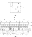
- the driving thin film transistor Td When the driving thin film transistor Td is turned on by the data signal, an electric current flowing through the light-emitting diode D is controlled, thereby displaying an image.
- the light-emitting diode D emits light due to the current supplied through the driving thin film transistor Td from the high voltage supply VDD.
- the first electrode 141 may be an anode or cathode for supplying one of holes or electrons to a light-emitting layer 142.
- a case in which the first electrode 141 of the electroluminescent display device 100 according to the first embodiment of the present disclosure is an anode will be described as an example.
- the first electrode 141 may be connected to the source electrode 132 of each of the thin film transistors Td1, Td2, and Td3 through the third contact hole CH3 formed in the passivation layer 134 and may be separately formed in each of the pixel regions SP1, SP2, and SP3.
- the electroluminescent display device 100 has been described by assuming that the thin film transistors Td1, Td2, and Td3 are N-type thin film transistors and the first electrode 141 is connected to the source electrode 132, embodiments are not limited thereto.
- the first electrode 141 may be connected to the drain electrode 130.
- the light-emitting layer 142 may emit white light.
- the light-emitting layer 142 may have a tandem white structure in which a plurality of light-emitting layers are stacked to emit white light.
- the light-emitting layer 142 may include a first light-emitting layer configured to emit blue light and a second light-emitting layer disposed on the first light-emitting layer and configured to emit light having a color which turns white when mixed with blue.
- the second light-emitting layer may be a light-emitting layer configured to emit yellow-green light.
- a light-emitting layer 142 configured to emit one of blue light, red light, and green light may be disposed in each of the pixel regions SP1, SP2, and SP3.
- a second electrode 143 for supplying one of electrons or holes to the light-emitting layer 142 may be disposed on the light-emitting layer 142.
- the first electrode 141, the insulating pattern IP, the light-emitting layer 142, and the second electrode 143 may overlap with each other and form each of the light emitting diodes D1, D2, and D3, and the light emitting diodes D1, D2, and D3 may be spaced apart from each other and be disposed corresponding to the pixel regions SP1, SP2, and SP3, respectively.
- a groove may be formed in the encapsulation film 171 corresponding to a boundary between the pixel regions SP1, SP2, and SP3.
- the encapsulation film 171 may be formed of an inorganic film and/or may have a multilayer structure.
- the first partition wall PW1 which is bar-shaped, may be disposed in the groove of the encapsulation film 171 corresponding to the boundary between the pixel regions SP1, SP2, and SP3.
- the first partition wall PW1 may be an organic material having the second refractive index lower than the first refractive index of the encapsulation film 171.
- the first refractive index may be in a range of 1.56 to 1.85
- the second refractive index may be in a range of 1.0 to 1.55, but embodiments are not limited thereto.
- the color filter layer 180 may be disposed on the encapsulation layer 170.
- the second partition wall PW2 having a refractive index lower than that of the color filter patterns 181, 183, and 185, light that is incident obliquely on the color filter patterns 181, 183, and 185 from the light-emitting layer 142 of the light emitting diodes D1, D2, and D3 may be reflected by the second partition wall PW2 and be output to upper areas of the corresponding pixel regions SP1, SP2, and SP3. Accordingly, a problem in which color mixture occurs in a viewing angle direction may be prevented.
- An interlayer insulating layer 128 and a passivation layer 134 may be disposed between the substrate 110 of FIG. 2 and the light emitting diodes D.
- the light emitting diodes D may be formed corresponding to the pixel regions SP.
- a bank layer which is formed in a conventional electroluminescent display device in order to partition pixel regions SP may be omitted, and a process may be simplified.
- the light-emitting layer 142 is formed to have a relatively small thickness on a stepped area of the first electrode 141 so that a current which does not contribute to emission is prevented from being focused, and current efficiency is improved.
- the first electrode 141, the insulating pattern IP, the light-emitting layer 142, and the second electrode 143 may form the light emitting diodes D, and adjacent light emitting diodes D may be spaced apart from each other and be disposed corresponding to the pixel regions SP.
- a middle portion of the first partition wall PW1 may have a bar shape, and an upper portion of the first partition wall PW1 may have a shape in which a width progressively increases upward.
- a width d1 of the middle portion of the first partition wall PW1 may be in a range of 2 ⁇ m to 3 ⁇ m.
- the width of the upper portion of the first partition wall PW1 may be larger than or equal to the width d1 of the middle portion of the first partition wall PW1.
- embodiments are not limited thereto, and the widths of the upper portion and the middle portion of the first partition wall PW1 may be modified in various ways according to the size, resolution, and the like of the pixel regions SP.
- a height HI of the first partition wall PW1 may be in a range of 7 ⁇ m to 9 ⁇ m, but embodiments are not limited thereto.
- the height HI may be modified in various ways according to a thickness or the like of the passivation layer 134, the interlayer insulating layer 128, and the light emitting diodes D.
- the first partition wall PW1 may be an organic material having a second refractive index lower than the first refractive index of the encapsulation film 171.
- the first refractive index may be in a range of 1.6 to 1.85
- the second refractive index may be in a range of 1.0 to 1.55, but embodiments are not limited thereto.
- An insulating pattern IP configured to cover a side surface and a portion of an upper surface of the first electrode 241 may be disposed.
- the interlayer insulating layer 228 and the passivation layer 234 of the electroluminescent display device 200 according to the second embodiment of the present disclosure have the under-cut form, the light-emitting layer 242 separately formed in each of the pixel regions SP1, SP2, and SP3 may be formed by one process.
- the residual layer OM is formed from materials, which are to be used in forming the light emitting diodes D1, D2, and D3 and the encapsulation film 271, remaining in the hole h1 of the interlayer insulating layer 228.
- the first partition wall PW1 having a refractive index lower than that of the encapsulation film 271
- light that is incident obliquely on the encapsulation film 271 from the light-emitting layer 242 of the light emitting diodes D1, D2, and D3 may be reflected by the first partition wall PW1 and be output to upper areas of the corresponding pixel regions SP1, SP2, and SP3. Accordingly, light extraction efficiency of the electroluminescent display device 200 may be improved, and color mixture may be prevented.
- permeation of oxygen or moisture into the light-emitting layer 242 and the second electrode 243 may be more effectively prevented by the encapsulation films 271 and the first partition wall PW1 disposed between the encapsulation films 271 configured to cover the light emitting diodes D1, D2, and D3.
- the color filter layer 280 may be disposed on the encapsulation layer 270.
- the color filter patterns 281, 283, and 285 have a third refractive index, and the second partition wall PW2 may have a fourth refractive index lower than the third refractive index.
- the second partition wall PW2 may be formed of silicon oxide, but embodiments are not limited thereto.
- the second partition wall PW2 having a refractive index lower than that of the color filter patterns 281, 283, and 285, light that is incident obliquely on the color filter patterns 281, 283, and 285 from the light-emitting layer 242 of the light emitting diodes D1, D2, and D3 may be reflected by the second partition wall PW2 and be output to upper areas of the corresponding pixel regions SP1, SP2, and SP3. Accordingly, a problem in which color mixture occurs in a viewing angle direction may be prevented.
- the second partition wall PW2 between the color filter patterns 281, 283, and 285 has a relatively fine width, an emissive area may be increased in comparison to a conventional case in which a black matrix is disposed.
- the second partition wall PW2 of the electroluminescent display device 200 according to the second embodiment of the present disclosure are formed corresponding to the first partition wall PW1.
- first partition wall PW1 and the second partition wall PW2 being disposed to be parallel to each other in the first direction, light that is output from the light emitting diodes D1, D2, and D3 respectively formed in the pixel regions SP1, SP2, and SP3 may be output to upper areas of the corresponding pixel regions SP1, SP2, and SP3. Accordingly, light extraction efficiency may be improved, and color mixture may be effectively prevented.
- the electroluminescent display device 200 has an under-cut form in which the width of the interlayer insulating layer 228 is smaller than the width of the passivation layer 234 disposed in each of the pixel regions SP.
- the first electrode 241 separately formed in each of the pixel regions SP may be formed by one process so that the process may be simplified.
- An insulating pattern IP configured to cover a side surface and a portion of an upper surface of the first electrode 241 may be disposed.
- the light-emitting layer 242 separately formed in each of the pixel regions SP may be formed by one process.
- the first electrode 241, the insulating pattern IP, the light-emitting layer 242, and the second electrode 243 may form each of the light emitting diodes D, and the light emitting diodes D may be separated from each other and disposed corresponding to the pixel regions SP, respectively.
- the encapsulation layer 270 may be disposed on the light emitting diodes D formed corresponding to the pixel regions SP, respectively.
- the encapsulation layer 270 may include an encapsulation film 271 having a first refractive index and a first partition wall PW1 having a second refractive index lower than the first refractive index.
- the encapsulation film 271 may be disposed in the form in which the encapsulation film 271 covers each of the light emitting diodes D formed corresponding to each of the pixel regions SP.
- the encapsulation film 271 may be formed of an inorganic film and/or have a multilayer structure.
- a residual layer OM may be present between the light emitting diodes D.
- the residual layer OM is formed from materials, which are to be used in forming the light emitting diodes D and the encapsulation film 271, remaining in the hole h1 of the interlayer insulating layer 228.
- the first partition wall PW1 may be disposed between the encapsulation films 271 corresponding to the boundary between the pixel regions SP.
- first partition wall PW1 is illustrated as having a bar shape and an upper portion of the first partition wall PW1 is illustrated as having a shape in which a width progressively increases in the drawings, this is merely an example.
- the first partition wall PW1 may be formed such that the upper portion and the middle portion have the same width.
- a lower portion of the first partition wall PW1 of the electroluminescent display device 200 according to the second embodiment of the present disclosure may be formed to have a width larger than that of the middle portion, and a lower surface of the first partition wall PW1 may contact the residual layer OM.
- a width d1 of the middle portion of the first partition wall PW1 may be in a range of 2 ⁇ m to 3 ⁇ m.
- the width of the upper portion of the first partition wall PW1 may be larger than or equal to the width d1 of the middle portion of the first partition wall PW1.
- embodiments are not limited thereto, and the size and form of the first partition wall PW1 may be modified in various ways according to the size, resolution, and the like of the pixel regions SP.
- a height HI of the first partition wall PW1 may be in a range of 7 ⁇ m to 9 ⁇ m, but embodiments are not limited thereto.
- the height HI may be modified in various ways according to a thickness or the like of the passivation layer 234, the interlayer insulating layer 228, and the light emitting diodes D.
- the first partition wall PW1 may be an organic material having a second refractive index lower than the first refractive index of the encapsulation film 271.
- the first refractive index may be in a range of 1.6 to 1.85
- the second refractive index may be in a range of 1.0 to 1.55, but embodiments are not limited thereto.
- the color filter layer 280 is disposed on the encapsulation layer 270.
- a width d2 of a middle portion of the second partition wall PW2 may be in a range of 2 ⁇ m to 3 ⁇ m.
- the width of an upper portion of the second partition wall PW2 may be larger than or equal to the width d2 of the middle portion of the second partition wall PW2.
- embodiments are not limited thereto.
- a height H2 of the second partition wall PW2 may be in a range of 7 ⁇ m to 9 ⁇ m, but embodiments are not limited thereto.
- the height H2 may be modified in various ways according to a thickness or the like of the color filter patterns 281, 283, and 285.
- the second partition wall PW2 between the color filter patterns 281, 283, and 285 has a relatively fine width d2, an emissive area may be increased in comparison to the conventional case in which a black matrix is disposed.
- the scattering layer SL may be a concavo-convex pattern formed on the upper surface of each of the color filter patterns 281, 283, and 285, but embodiments are not limited thereto.
- the scattering layer SL may also be formed of a material layer including beads.
- first partition wall PW1 and the second partition wall PW2 may be disposed to be parallel to each other in a first direction 1A perpendicular to the substrate 110.
- a path of light that is obliquely output outward from light emitting diodes D may be adjusted through the first and second partition walls PW1 and PW2 of FIG. 5 and a largest amount of light may be output to the outside when the refractive indices of the first and second partition walls PW1 and PW2 of FIG. 5 are 1.4.
Landscapes
- Physics & Mathematics (AREA)
- Optics & Photonics (AREA)
- Chemical & Material Sciences (AREA)
- Inorganic Chemistry (AREA)
- Engineering & Computer Science (AREA)
- Microelectronics & Electronic Packaging (AREA)
- Electroluminescent Light Sources (AREA)
- Optical Elements Other Than Lenses (AREA)
- Optical Filters (AREA)
- Devices For Indicating Variable Information By Combining Individual Elements (AREA)
Claims (11)
- Dispositif d'affichage électroluminescent comportant :un substrat (110, 210) incluant une pluralité de régions de pixels (SP) ;une pluralité de diodes électroluminescentes (D) espacées les unes des autres sur le substrat (110, 210) et correspondant à la pluralité de régions de pixels (SP), respectivement ;un film d'encapsulation (171, 271) recouvrant respectivement la pluralité de diodes électroluminescentes (D) et ayant un premier indice de réfraction ;une première paroi de séparation (PW1) disposée entre le film d'encapsulation (171, 271) correspondant à une frontière entre la pluralité de régions de pixels (SP) et ayant un deuxième indice de réfraction inférieur au premier indice de réfraction ; etune couche de filtre à couleur (180, 280) disposée sur le film d'encapsulation (171, 271) et la première paroi de séparation (PW1), dans lequel la couche de filtre à couleur (180, 280) inclut une pluralité de motifs de filtre à couleur (181, 183, 185 ; 281, 283, 285) ayant un troisième indice de réfraction et une seconde paroi de séparation (PW2) disposée entre la pluralité de motifs de filtre à couleur (181, 183, 185 ; 281, 283, 285) et ayant un quatrième indice de réfraction inférieur au troisième indice de réfraction,dans lequel la seconde paroi de séparation (PW2) est disposée en correspondance avec la première paroi de séparation (PW1), etdans lequel les motifs de la pluralité de motifs de filtre à couleur (181, 183, 185 ; 281, 283, 285) sont disposés de manière à correspondre à la pluralité de diodes électroluminescentes (D), respectivement.
- Dispositif d'affichage électroluminescent selon la revendication 1, dans lequel une partie centrale de chaque paroi parmi la première paroi de séparation (PW1) et/ou la seconde paroi de séparation (PW2) a une forme de barre.
- Dispositif d'affichage électroluminescent selon l'une quelconque des revendications précédentes, dans lequel une partie supérieure de chaque paroi parmi la première paroi de séparation (PW1) et la seconde paroi de séparation (PW2) a une largeur qui augmente progressivement vers le haut.
- Dispositif d'affichage électroluminescent selon la revendication 2 ou 3, dans lequel
une largeur de la partie centrale de chaque paroi parmi la première paroi de séparation (PW1) et/ou la seconde paroi de séparation (PW2) est dans un intervalle de 2 µm à 3 µm ;
et/ou
une hauteur de chaque paroi parmi la première paroi de séparation (PW1) et/ou la seconde paroi de séparation (PW2) est dans un intervalle de 7 µm à 9 µm. - Dispositif d'affichage électroluminescent selon l'une quelconque des revendications précédentes, dans lequel chaque indice parmi le deuxième indice de réfraction et/ou le quatrième indice de réfraction est dans un intervalle de 1,0 à 1,55.
- Dispositif d'affichage électroluminescent selon l'une quelconque des revendications précédentes, dans lequel la couche de filtre à couleur (180, 280) inclut en outre une couche de diffusion (SL) disposée sur une surface supérieure de chaque motif parmi la pluralité de motifs de filtre à couleur (181, 183, 185 ; 281, 283, 285) ; et/ou un bord de chaque motif parmi la pluralité de motifs de filtre à couleur (181, 183, 185 ; 281, 283, 285) est incurvé.
- Dispositif d'affichage électroluminescent selon l'une quelconque des revendications précédentes, dans lequel chaque diode parmi la pluralité de diodes électroluminescentes (D) inclut :une première électrode (141, 241) disposée sur une couche de passivation (134, 234);un motif isolant (IP) configuré pour recouvrir un bord de la première électrode (141, 241) ;une couche émettrice de lumière (142, 242) disposée sur la première électrode (141, 241) et le motif isolant (IP) ; etune seconde électrode (143, 243) disposée sur la couche émettrice de lumière (142, 242).
- Dispositif d'affichage électroluminescent selon la revendication 7, incluant en outre une couche d'isolation intercouche (128, 228) disposée sous la couche de passivation (134, 234), dans lequel la couche de passivation (134, 234) et la couche d'isolation intercouche (128, 228) pour chaque région de pixel (SP) sont séparées par la première paroi de séparation (PW1).
- Dispositif d'affichage électroluminescent selon l'une quelconque des revendications précédentes, dans lequel deux diodes électroluminescentes (D1, D2 et D3) adjacentes sont séparées par un trou (h) dans la couche de passivation (134) et la couche d'isolation intercouche (128).
- Dispositif d'affichage électroluminescent selon l'une quelconque des revendications précédentes, dans lequel une couche d'encapsulation (170) inclut le film d'encapsulation (171) ayant le premier indice de réfraction et la première paroi de séparation (PW1) ayant un deuxième indice de réfraction inférieur au premier indice de réfraction.
- Dispositif d'affichage électroluminescent selon la revendication 8, comportant en outre un trou (h) ayant différentes parties (h1) et (h2) configurées pour séparer les régions de pixels (SP1, SP2, SP3) dans la couche d'isolation intercouche (228) et la couche de passivation (234), dans lequel une largeur d'une première partie (h1) est supérieure à une largeur d'une seconde partie (h2).
Applications Claiming Priority (1)
| Application Number | Priority Date | Filing Date | Title |
|---|---|---|---|
| KR1020170166006A KR102431686B1 (ko) | 2017-12-05 | 2017-12-05 | 전계발광 표시장치 |
Publications (2)
| Publication Number | Publication Date |
|---|---|
| EP3496176A1 EP3496176A1 (fr) | 2019-06-12 |
| EP3496176B1 true EP3496176B1 (fr) | 2020-04-22 |
Family
ID=64650129
Family Applications (1)
| Application Number | Title | Priority Date | Filing Date |
|---|---|---|---|
| EP18210235.0A Active EP3496176B1 (fr) | 2017-12-05 | 2018-12-04 | Afficheur électroluminescent |
Country Status (6)
| Country | Link |
|---|---|
| US (1) | US10700140B2 (fr) |
| EP (1) | EP3496176B1 (fr) |
| JP (1) | JP6705882B2 (fr) |
| KR (1) | KR102431686B1 (fr) |
| CN (1) | CN109950278B (fr) |
| TW (1) | TWI694610B (fr) |
Families Citing this family (39)
| Publication number | Priority date | Publication date | Assignee | Title |
|---|---|---|---|---|
| WO2020105433A1 (fr) * | 2018-11-20 | 2020-05-28 | ソニーセミコンダクタソリューションズ株式会社 | Dispositif d'affichage, procédé de fabrication de dispositif d'affichage et dispositif électronique |
| US11861941B1 (en) | 2019-02-06 | 2024-01-02 | Apple Inc. | Eye camera systems with polarized light |
| US11326763B1 (en) | 2019-02-06 | 2022-05-10 | Apple Inc. | Light-emitting diodes with optical filters |
| CN110021647A (zh) * | 2019-03-27 | 2019-07-16 | 武汉华星光电半导体显示技术有限公司 | 一种oled显示面板及其制备方法 |
| KR102774371B1 (ko) * | 2019-07-30 | 2025-03-04 | 엘지이노텍 주식회사 | 광 경로 제어 부재 및 이를 포함하는 표시 장치 |
| CN110473984B (zh) * | 2019-08-27 | 2021-12-24 | 昆山工研院新型平板显示技术中心有限公司 | 显示面板、显示装置及显示面板的制备方法 |
| JP2021086769A (ja) * | 2019-11-29 | 2021-06-03 | パナソニックIpマネジメント株式会社 | 発光デバイス及びそれを備えたディスプレイパネル及びその製造方法 |
| US12317713B2 (en) * | 2019-12-12 | 2025-05-27 | Sharp Kabushiki Kaisha | Display device |
| CN111063713B (zh) * | 2019-12-12 | 2022-03-29 | 武汉华星光电半导体显示技术有限公司 | 一种oled显示面板、其制备方法及其终端装置 |
| KR102914155B1 (ko) * | 2019-12-30 | 2026-01-16 | 엘지디스플레이 주식회사 | 유기 발광 표시 장치 |
| US11980046B2 (en) | 2020-05-27 | 2024-05-07 | Taiwan Semiconductor Manufacturing Company, Ltd. | Method for forming an isolation structure having multiple thicknesses to mitigate damage to a display device |
| TWI737484B (zh) * | 2020-06-05 | 2021-08-21 | 友達光電股份有限公司 | 顯示裝置 |
| CN111864105A (zh) * | 2020-07-09 | 2020-10-30 | 武汉华星光电半导体显示技术有限公司 | 显示面板及其制备方法 |
| KR102761522B1 (ko) * | 2020-08-14 | 2025-02-04 | 삼성디스플레이 주식회사 | 표시 장치 및 그 제조방법 |
| WO2022038452A1 (fr) * | 2020-08-21 | 2022-02-24 | 株式会社半導体エネルギー研究所 | Dispositif d'affichage, dispositif électronique et visiocasque |
| CN114388560B (zh) * | 2020-10-22 | 2024-08-23 | 京东方科技集团股份有限公司 | 显示面板及其制备方法、显示装置 |
| KR20220065925A (ko) * | 2020-11-13 | 2022-05-23 | 삼성디스플레이 주식회사 | 표시 패널 및 전자 장치 |
| KR20220099595A (ko) * | 2021-01-06 | 2022-07-14 | 삼성디스플레이 주식회사 | 표시 장치 |
| TW202243239A (zh) * | 2021-01-08 | 2022-11-01 | 日商索尼集團公司 | 顯示裝置及電子機器 |
| US20240306423A1 (en) * | 2021-01-14 | 2024-09-12 | Semiconductor Energy Laboratory Co., Ltd. | Light-Emitting Element, Display Apparatus, and Electronic Device |
| WO2022200916A1 (fr) * | 2021-03-25 | 2022-09-29 | 株式会社半導体エネルギー研究所 | Dispositif d'affichage, procédé de fabrication pour dispositif d'affichage, module d'affichage et appareil électronique |
| CN112952025A (zh) * | 2021-03-31 | 2021-06-11 | 京东方科技集团股份有限公司 | 显示基板及显示装置 |
| KR102866873B1 (ko) * | 2021-04-30 | 2025-10-01 | 삼성디스플레이 주식회사 | 표시 장치 및 표시 장치의 제조 방법 |
| KR20240047992A (ko) * | 2021-08-12 | 2024-04-12 | 가부시키가이샤 한도오따이 에네루기 켄큐쇼 | 표시 장치 및 표시 장치의 제작 방법 |
| JPWO2023017357A1 (fr) * | 2021-08-12 | 2023-02-16 | ||
| CN117898024A (zh) * | 2021-08-27 | 2024-04-16 | 株式会社半导体能源研究所 | 显示装置 |
| KR20230033179A (ko) * | 2021-08-30 | 2023-03-08 | 삼성디스플레이 주식회사 | 표시패널 및 이의 제조방법 |
| JPWO2023052906A1 (fr) * | 2021-09-30 | 2023-04-06 | ||
| WO2023089443A1 (fr) * | 2021-11-18 | 2023-05-25 | 株式会社半導体エネルギー研究所 | Dispositif d'affichage et procédé de production de dispositif d'affichage |
| JPWO2023089447A1 (fr) * | 2021-11-19 | 2023-05-25 | ||
| US20250098429A1 (en) * | 2021-12-29 | 2025-03-20 | Semiconductor Energy Laboratory Co., Ltd. | Display device, display module, and electronic device |
| JPWO2023126738A1 (fr) * | 2021-12-29 | 2023-07-06 | ||
| TW202415140A (zh) | 2022-03-16 | 2024-04-01 | 日商索尼半導體解決方案公司 | 發光裝置及電子機器 |
| WO2024144018A1 (fr) * | 2022-12-30 | 2024-07-04 | 주식회사 야스 | Dispositif d'affichage électroluminescent organique |
| WO2025023242A1 (fr) * | 2023-07-26 | 2025-01-30 | ソニーセミコンダクタソリューションズ株式会社 | Dispositif d'affichage et appareil électronique |
| KR20250019823A (ko) * | 2023-08-02 | 2025-02-11 | 삼성전자주식회사 | 디스플레이 장치 및 이의 제조 방법 |
| TWI855823B (zh) * | 2023-08-16 | 2024-09-11 | 友達光電股份有限公司 | 顯示面板 |
| FR3161088A1 (fr) * | 2024-04-04 | 2025-10-10 | Commissariat A L' Energie Atomique Et Aux Energies Alternatives | Procédé de fabrication d’un dispositif d’affichage electroluminescent, dispositif d’affichage electroluminescent |
| KR20260010591A (ko) * | 2024-07-12 | 2026-01-21 | 삼성디스플레이 주식회사 | 표시 패널, 이를 포함하는 전자 장치, 및 표시 패널의 제조 방법 |
Family Cites Families (29)
| Publication number | Priority date | Publication date | Assignee | Title |
|---|---|---|---|---|
| CN1685769B (zh) * | 2003-06-13 | 2011-05-11 | 富士电机控股株式会社 | 有机el显示器 |
| KR100643404B1 (ko) * | 2005-09-22 | 2006-11-10 | 삼성전자주식회사 | 디스플레이장치 및 그 제조방법 |
| KR100759668B1 (ko) * | 2006-03-08 | 2007-09-17 | 삼성에스디아이 주식회사 | 유기 전계 발광표시장치 및 그의 제조방법 |
| JP5762746B2 (ja) | 2007-11-14 | 2015-08-12 | クゥアルコム・インコーポレイテッドQualcomm Incorporated | 地理的ユーザプロファイルに基づいてターゲット・コンテンツ・メッセージの適切性を決定するように地理的ユーザプロファイルを決定するための方法およびシステム |
| KR101156435B1 (ko) * | 2010-01-08 | 2012-06-18 | 삼성모바일디스플레이주식회사 | 유기 발광 표시 장치 |
| JP5708152B2 (ja) * | 2011-03-31 | 2015-04-30 | ソニー株式会社 | 表示装置およびその製造方法 |
| JP2013258021A (ja) * | 2012-06-12 | 2013-12-26 | Canon Inc | 表示装置 |
| KR101941178B1 (ko) * | 2012-09-28 | 2019-01-23 | 삼성디스플레이 주식회사 | 유기 발광 표시 장치 및 유기 발광 표시 장치의 제조 방법 |
| KR102051103B1 (ko) * | 2012-11-07 | 2019-12-03 | 삼성디스플레이 주식회사 | 유기 발광 표시 장치 |
| JP2014127441A (ja) * | 2012-12-27 | 2014-07-07 | Sony Corp | 表示装置、表示装置の製造方法および電子機器 |
| KR102048924B1 (ko) * | 2013-05-16 | 2019-11-27 | 삼성디스플레이 주식회사 | 유기발광표시장치 |
| KR102111974B1 (ko) * | 2013-07-03 | 2020-05-19 | 삼성디스플레이 주식회사 | 유기발광 표시 장치 및 이의 제조 방법 |
| JP6275439B2 (ja) * | 2013-09-30 | 2018-02-07 | 株式会社ジャパンディスプレイ | エレクトロルミネセンス装置およびその製造方法 |
| KR20150043136A (ko) * | 2013-10-14 | 2015-04-22 | 삼성디스플레이 주식회사 | 유기 발광 표시 장치 및 이의 제조 방법 |
| KR102295610B1 (ko) * | 2013-12-27 | 2021-08-30 | 엘지디스플레이 주식회사 | 유기 발광 다이오드 표시 장치 |
| KR102205356B1 (ko) * | 2014-01-29 | 2021-01-21 | 삼성디스플레이 주식회사 | 표시 패널 및 이의 제조 방법 |
| JP6439255B2 (ja) * | 2014-02-27 | 2018-12-19 | 大日本印刷株式会社 | 有機エレクトロルミネッセンス表示装置およびその製造方法 |
| KR102360089B1 (ko) * | 2014-08-05 | 2022-02-09 | 삼성디스플레이 주식회사 | 유기 발광 표시 장치 및 그 제조방법 |
| KR20160034457A (ko) * | 2014-09-19 | 2016-03-30 | 삼성디스플레이 주식회사 | 유기발광 표시장치 |
| CN104659070B (zh) * | 2015-03-13 | 2018-11-16 | 上海天马有机发光显示技术有限公司 | 一种显示面板、显示装置及显示面板的制造方法 |
| JP6601047B2 (ja) * | 2015-08-07 | 2019-11-06 | ソニー株式会社 | 発光素子及びその製造方法、並びに、表示装置 |
| JP2017073260A (ja) * | 2015-10-06 | 2017-04-13 | 株式会社ジャパンディスプレイ | 有機el表示装置及び有機el表示装置の製造方法 |
| KR102419033B1 (ko) * | 2015-12-28 | 2022-07-08 | 엘지디스플레이 주식회사 | 유기발광 디스플레이 패널 및 이를 포함하는 유기발광 디스플레이 장치 |
| JP2018081815A (ja) * | 2016-11-16 | 2018-05-24 | 株式会社ジャパンディスプレイ | 表示装置 |
| JP6823443B2 (ja) * | 2016-12-07 | 2021-02-03 | キヤノン株式会社 | 表示装置およびその製造方法 |
| KR102663231B1 (ko) * | 2016-12-30 | 2024-05-02 | 엘지디스플레이 주식회사 | 유기발광 표시장치 |
| KR102416417B1 (ko) * | 2017-11-24 | 2022-07-04 | 삼성디스플레이 주식회사 | 표시 장치 및 그 제조 방법 |
| KR102433274B1 (ko) * | 2017-11-28 | 2022-08-18 | 삼성디스플레이 주식회사 | 유기 발광 표시 장치 |
| KR102533686B1 (ko) * | 2018-01-18 | 2023-05-17 | 삼성디스플레이 주식회사 | 표시 장치 및 그 제조 방법 |
-
2017
- 2017-12-05 KR KR1020170166006A patent/KR102431686B1/ko active Active
-
2018
- 2018-11-27 TW TW107142310A patent/TWI694610B/zh active
- 2018-12-03 CN CN201811467049.2A patent/CN109950278B/zh active Active
- 2018-12-04 EP EP18210235.0A patent/EP3496176B1/fr active Active
- 2018-12-04 JP JP2018227510A patent/JP6705882B2/ja active Active
- 2018-12-05 US US16/210,375 patent/US10700140B2/en active Active
Non-Patent Citations (1)
| Title |
|---|
| None * |
Also Published As
| Publication number | Publication date |
|---|---|
| US10700140B2 (en) | 2020-06-30 |
| TWI694610B (zh) | 2020-05-21 |
| KR20190066359A (ko) | 2019-06-13 |
| KR102431686B1 (ko) | 2022-08-10 |
| TW201926294A (zh) | 2019-07-01 |
| EP3496176A1 (fr) | 2019-06-12 |
| JP6705882B2 (ja) | 2020-06-03 |
| US20190172874A1 (en) | 2019-06-06 |
| CN109950278A (zh) | 2019-06-28 |
| CN109950278B (zh) | 2023-06-13 |
| JP2019102462A (ja) | 2019-06-24 |
Similar Documents
| Publication | Publication Date | Title |
|---|---|---|
| EP3496176B1 (fr) | Afficheur électroluminescent | |
| CN110021637B (zh) | 电致发光显示装置 | |
| CN109904191B (zh) | 电致发光显示装置 | |
| US11063244B2 (en) | Electroluminescent display device | |
| EP3188276B1 (fr) | Afficheur à diode électroluminescente organique | |
| KR102690328B1 (ko) | 유기발광다이오드 표시장치 | |
| EP3462514B1 (fr) | Afficheur électroluminescent | |
| US9997572B2 (en) | Display device having a light scattering structure | |
| KR102383928B1 (ko) | 전계발광 표시장치 | |
| KR20180077856A (ko) | 전계발광 표시장치 | |
| KR102577043B1 (ko) | 전계발광 표시장치 | |
| KR20130093187A (ko) | 유기 발광 표시 장치 및 그 제조 방법 | |
| US10062736B2 (en) | Display device having varying distances between reflecting layers | |
| KR102455567B1 (ko) | 전계발광 표시장치 | |
| US10720597B2 (en) | Electroluminescent display device | |
| CN118414019A (zh) | 有机发光二极管显示装置及其制造方法 | |
| KR20180013469A (ko) | 유기발광다이오드 표시장치 | |
| KR20180077834A (ko) | 전계발광 표시장치 | |
| KR20200061624A (ko) | 표시장치 | |
| KR20180061777A (ko) | 유기발광다이오드 표시장치 | |
| KR102503745B1 (ko) | 전계발광 표시장치 |
Legal Events
| Date | Code | Title | Description |
|---|---|---|---|
| PUAI | Public reference made under article 153(3) epc to a published international application that has entered the european phase |
Free format text: ORIGINAL CODE: 0009012 |
|
| STAA | Information on the status of an ep patent application or granted ep patent |
Free format text: STATUS: REQUEST FOR EXAMINATION WAS MADE |
|
| 17P | Request for examination filed |
Effective date: 20181204 |
|
| AK | Designated contracting states |
Kind code of ref document: A1 Designated state(s): AL AT BE BG CH CY CZ DE DK EE ES FI FR GB GR HR HU IE IS IT LI LT LU LV MC MK MT NL NO PL PT RO RS SE SI SK SM TR |
|
| AX | Request for extension of the european patent |
Extension state: BA ME |
|
| RBV | Designated contracting states (corrected) |
Designated state(s): AL AT BE BG CH CY CZ DE DK EE ES FI FR GB GR HR HU IE IS IT LI LT LU LV MC MK MT NL NO PL PT RO RS SE SI SK SM TR |
|
| GRAP | Despatch of communication of intention to grant a patent |
Free format text: ORIGINAL CODE: EPIDOSNIGR1 |
|
| STAA | Information on the status of an ep patent application or granted ep patent |
Free format text: STATUS: GRANT OF PATENT IS INTENDED |
|
| INTG | Intention to grant announced |
Effective date: 20191127 |
|
| GRAS | Grant fee paid |
Free format text: ORIGINAL CODE: EPIDOSNIGR3 |
|
| GRAA | (expected) grant |
Free format text: ORIGINAL CODE: 0009210 |
|
| STAA | Information on the status of an ep patent application or granted ep patent |
Free format text: STATUS: THE PATENT HAS BEEN GRANTED |
|
| AK | Designated contracting states |
Kind code of ref document: B1 Designated state(s): AL AT BE BG CH CY CZ DE DK EE ES FI FR GB GR HR HU IE IS IT LI LT LU LV MC MK MT NL NO PL PT RO RS SE SI SK SM TR |
|
| REG | Reference to a national code |
Ref country code: CH Ref legal event code: EP |
|
| REG | Reference to a national code |
Ref country code: IE Ref legal event code: FG4D |
|
| REG | Reference to a national code |
Ref country code: DE Ref legal event code: R096 Ref document number: 602018003995 Country of ref document: DE |
|
| REG | Reference to a national code |
Ref country code: AT Ref legal event code: REF Ref document number: 1261312 Country of ref document: AT Kind code of ref document: T Effective date: 20200515 |
|
| REG | Reference to a national code |
Ref country code: LT Ref legal event code: MG4D |
|
| REG | Reference to a national code |
Ref country code: NL Ref legal event code: MP Effective date: 20200422 |
|
| PG25 | Lapsed in a contracting state [announced via postgrant information from national office to epo] |
Ref country code: NL Free format text: LAPSE BECAUSE OF FAILURE TO SUBMIT A TRANSLATION OF THE DESCRIPTION OR TO PAY THE FEE WITHIN THE PRESCRIBED TIME-LIMIT Effective date: 20200422 Ref country code: SE Free format text: LAPSE BECAUSE OF FAILURE TO SUBMIT A TRANSLATION OF THE DESCRIPTION OR TO PAY THE FEE WITHIN THE PRESCRIBED TIME-LIMIT Effective date: 20200422 Ref country code: FI Free format text: LAPSE BECAUSE OF FAILURE TO SUBMIT A TRANSLATION OF THE DESCRIPTION OR TO PAY THE FEE WITHIN THE PRESCRIBED TIME-LIMIT Effective date: 20200422 Ref country code: NO Free format text: LAPSE BECAUSE OF FAILURE TO SUBMIT A TRANSLATION OF THE DESCRIPTION OR TO PAY THE FEE WITHIN THE PRESCRIBED TIME-LIMIT Effective date: 20200722 Ref country code: LT Free format text: LAPSE BECAUSE OF FAILURE TO SUBMIT A TRANSLATION OF THE DESCRIPTION OR TO PAY THE FEE WITHIN THE PRESCRIBED TIME-LIMIT Effective date: 20200422 Ref country code: PT Free format text: LAPSE BECAUSE OF FAILURE TO SUBMIT A TRANSLATION OF THE DESCRIPTION OR TO PAY THE FEE WITHIN THE PRESCRIBED TIME-LIMIT Effective date: 20200824 Ref country code: GR Free format text: LAPSE BECAUSE OF FAILURE TO SUBMIT A TRANSLATION OF THE DESCRIPTION OR TO PAY THE FEE WITHIN THE PRESCRIBED TIME-LIMIT Effective date: 20200723 Ref country code: IS Free format text: LAPSE BECAUSE OF FAILURE TO SUBMIT A TRANSLATION OF THE DESCRIPTION OR TO PAY THE FEE WITHIN THE PRESCRIBED TIME-LIMIT Effective date: 20200822 |
|
| REG | Reference to a national code |
Ref country code: AT Ref legal event code: MK05 Ref document number: 1261312 Country of ref document: AT Kind code of ref document: T Effective date: 20200422 |
|
| PG25 | Lapsed in a contracting state [announced via postgrant information from national office to epo] |
Ref country code: BG Free format text: LAPSE BECAUSE OF FAILURE TO SUBMIT A TRANSLATION OF THE DESCRIPTION OR TO PAY THE FEE WITHIN THE PRESCRIBED TIME-LIMIT Effective date: 20200722 Ref country code: LV Free format text: LAPSE BECAUSE OF FAILURE TO SUBMIT A TRANSLATION OF THE DESCRIPTION OR TO PAY THE FEE WITHIN THE PRESCRIBED TIME-LIMIT Effective date: 20200422 Ref country code: HR Free format text: LAPSE BECAUSE OF FAILURE TO SUBMIT A TRANSLATION OF THE DESCRIPTION OR TO PAY THE FEE WITHIN THE PRESCRIBED TIME-LIMIT Effective date: 20200422 Ref country code: RS Free format text: LAPSE BECAUSE OF FAILURE TO SUBMIT A TRANSLATION OF THE DESCRIPTION OR TO PAY THE FEE WITHIN THE PRESCRIBED TIME-LIMIT Effective date: 20200422 |
|
| PG25 | Lapsed in a contracting state [announced via postgrant information from national office to epo] |
Ref country code: AL Free format text: LAPSE BECAUSE OF FAILURE TO SUBMIT A TRANSLATION OF THE DESCRIPTION OR TO PAY THE FEE WITHIN THE PRESCRIBED TIME-LIMIT Effective date: 20200422 |
|
| REG | Reference to a national code |
Ref country code: DE Ref legal event code: R097 Ref document number: 602018003995 Country of ref document: DE |
|
| PG25 | Lapsed in a contracting state [announced via postgrant information from national office to epo] |
Ref country code: AT Free format text: LAPSE BECAUSE OF FAILURE TO SUBMIT A TRANSLATION OF THE DESCRIPTION OR TO PAY THE FEE WITHIN THE PRESCRIBED TIME-LIMIT Effective date: 20200422 Ref country code: EE Free format text: LAPSE BECAUSE OF FAILURE TO SUBMIT A TRANSLATION OF THE DESCRIPTION OR TO PAY THE FEE WITHIN THE PRESCRIBED TIME-LIMIT Effective date: 20200422 Ref country code: DK Free format text: LAPSE BECAUSE OF FAILURE TO SUBMIT A TRANSLATION OF THE DESCRIPTION OR TO PAY THE FEE WITHIN THE PRESCRIBED TIME-LIMIT Effective date: 20200422 Ref country code: IT Free format text: LAPSE BECAUSE OF FAILURE TO SUBMIT A TRANSLATION OF THE DESCRIPTION OR TO PAY THE FEE WITHIN THE PRESCRIBED TIME-LIMIT Effective date: 20200422 Ref country code: RO Free format text: LAPSE BECAUSE OF FAILURE TO SUBMIT A TRANSLATION OF THE DESCRIPTION OR TO PAY THE FEE WITHIN THE PRESCRIBED TIME-LIMIT Effective date: 20200422 Ref country code: ES Free format text: LAPSE BECAUSE OF FAILURE TO SUBMIT A TRANSLATION OF THE DESCRIPTION OR TO PAY THE FEE WITHIN THE PRESCRIBED TIME-LIMIT Effective date: 20200422 Ref country code: CZ Free format text: LAPSE BECAUSE OF FAILURE TO SUBMIT A TRANSLATION OF THE DESCRIPTION OR TO PAY THE FEE WITHIN THE PRESCRIBED TIME-LIMIT Effective date: 20200422 Ref country code: SM Free format text: LAPSE BECAUSE OF FAILURE TO SUBMIT A TRANSLATION OF THE DESCRIPTION OR TO PAY THE FEE WITHIN THE PRESCRIBED TIME-LIMIT Effective date: 20200422 |
|
| PG25 | Lapsed in a contracting state [announced via postgrant information from national office to epo] |
Ref country code: SK Free format text: LAPSE BECAUSE OF FAILURE TO SUBMIT A TRANSLATION OF THE DESCRIPTION OR TO PAY THE FEE WITHIN THE PRESCRIBED TIME-LIMIT Effective date: 20200422 Ref country code: PL Free format text: LAPSE BECAUSE OF FAILURE TO SUBMIT A TRANSLATION OF THE DESCRIPTION OR TO PAY THE FEE WITHIN THE PRESCRIBED TIME-LIMIT Effective date: 20200422 |
|
| PLBE | No opposition filed within time limit |
Free format text: ORIGINAL CODE: 0009261 |
|
| STAA | Information on the status of an ep patent application or granted ep patent |
Free format text: STATUS: NO OPPOSITION FILED WITHIN TIME LIMIT |
|
| 26N | No opposition filed |
Effective date: 20210125 |
|
| PG25 | Lapsed in a contracting state [announced via postgrant information from national office to epo] |
Ref country code: SI Free format text: LAPSE BECAUSE OF FAILURE TO SUBMIT A TRANSLATION OF THE DESCRIPTION OR TO PAY THE FEE WITHIN THE PRESCRIBED TIME-LIMIT Effective date: 20200422 |
|
| PG25 | Lapsed in a contracting state [announced via postgrant information from national office to epo] |
Ref country code: MC Free format text: LAPSE BECAUSE OF FAILURE TO SUBMIT A TRANSLATION OF THE DESCRIPTION OR TO PAY THE FEE WITHIN THE PRESCRIBED TIME-LIMIT Effective date: 20200422 |
|
| REG | Reference to a national code |
Ref country code: BE Ref legal event code: MM Effective date: 20201231 |
|
| PG25 | Lapsed in a contracting state [announced via postgrant information from national office to epo] |
Ref country code: IE Free format text: LAPSE BECAUSE OF NON-PAYMENT OF DUE FEES Effective date: 20201204 Ref country code: LU Free format text: LAPSE BECAUSE OF NON-PAYMENT OF DUE FEES Effective date: 20201204 |
|
| PG25 | Lapsed in a contracting state [announced via postgrant information from national office to epo] |
Ref country code: TR Free format text: LAPSE BECAUSE OF FAILURE TO SUBMIT A TRANSLATION OF THE DESCRIPTION OR TO PAY THE FEE WITHIN THE PRESCRIBED TIME-LIMIT Effective date: 20200422 Ref country code: MT Free format text: LAPSE BECAUSE OF FAILURE TO SUBMIT A TRANSLATION OF THE DESCRIPTION OR TO PAY THE FEE WITHIN THE PRESCRIBED TIME-LIMIT Effective date: 20200422 Ref country code: CY Free format text: LAPSE BECAUSE OF FAILURE TO SUBMIT A TRANSLATION OF THE DESCRIPTION OR TO PAY THE FEE WITHIN THE PRESCRIBED TIME-LIMIT Effective date: 20200422 |
|
| PG25 | Lapsed in a contracting state [announced via postgrant information from national office to epo] |
Ref country code: MK Free format text: LAPSE BECAUSE OF FAILURE TO SUBMIT A TRANSLATION OF THE DESCRIPTION OR TO PAY THE FEE WITHIN THE PRESCRIBED TIME-LIMIT Effective date: 20200422 |
|
| PG25 | Lapsed in a contracting state [announced via postgrant information from national office to epo] |
Ref country code: BE Free format text: LAPSE BECAUSE OF NON-PAYMENT OF DUE FEES Effective date: 20201231 |
|
| REG | Reference to a national code |
Ref country code: CH Ref legal event code: PL |
|
| REG | Reference to a national code |
Ref country code: DE Ref legal event code: R079 Ref document number: 602018003995 Country of ref document: DE Free format text: PREVIOUS MAIN CLASS: H01L0051520000 Ipc: H10K0050800000 |
|
| PG25 | Lapsed in a contracting state [announced via postgrant information from national office to epo] |
Ref country code: LI Free format text: LAPSE BECAUSE OF NON-PAYMENT OF DUE FEES Effective date: 20211231 Ref country code: CH Free format text: LAPSE BECAUSE OF NON-PAYMENT OF DUE FEES Effective date: 20211231 |
|
| PGFP | Annual fee paid to national office [announced via postgrant information from national office to epo] |
Ref country code: DE Payment date: 20251020 Year of fee payment: 8 |
|
| PGFP | Annual fee paid to national office [announced via postgrant information from national office to epo] |
Ref country code: GB Payment date: 20251023 Year of fee payment: 8 |
|
| PGFP | Annual fee paid to national office [announced via postgrant information from national office to epo] |
Ref country code: FR Payment date: 20251021 Year of fee payment: 8 |