EP3496253B1 - Vorrichtung zur ansteuerung einer induktiven last - Google Patents
Vorrichtung zur ansteuerung einer induktiven last Download PDFInfo
- Publication number
- EP3496253B1 EP3496253B1 EP18204551.8A EP18204551A EP3496253B1 EP 3496253 B1 EP3496253 B1 EP 3496253B1 EP 18204551 A EP18204551 A EP 18204551A EP 3496253 B1 EP3496253 B1 EP 3496253B1
- Authority
- EP
- European Patent Office
- Prior art keywords
- inductive load
- current
- voltage
- switching element
- control
- Prior art date
- Legal status (The legal status is an assumption and is not a legal conclusion. Google has not performed a legal analysis and makes no representation as to the accuracy of the status listed.)
- Not-in-force
Links
Images


Classifications
-
- H—ELECTRICITY
- H03—ELECTRONIC CIRCUITRY
- H03K—PULSE TECHNIQUE
- H03K17/00—Electronic switching or gating, i.e. not by contact-making and –breaking
- H03K17/08—Modifications for protecting switching circuit against overcurrent or overvoltage
- H03K17/082—Modifications for protecting switching circuit against overcurrent or overvoltage by feedback from the output to the control circuit
- H03K17/0822—Modifications for protecting switching circuit against overcurrent or overvoltage by feedback from the output to the control circuit in field-effect transistor switches
-
- H—ELECTRICITY
- H02—GENERATION; CONVERSION OR DISTRIBUTION OF ELECTRIC POWER
- H02M—APPARATUS FOR CONVERSION BETWEEN AC AND AC, BETWEEN AC AND DC, OR BETWEEN DC AND DC, AND FOR USE WITH MAINS OR SIMILAR POWER SUPPLY SYSTEMS; CONVERSION OF DC OR AC INPUT POWER INTO SURGE OUTPUT POWER; CONTROL OR REGULATION THEREOF
- H02M3/00—Conversion of DC power input into DC power output
- H02M3/02—Conversion of DC power input into DC power output without intermediate conversion into AC
- H02M3/04—Conversion of DC power input into DC power output without intermediate conversion into AC by static converters
- H02M3/10—Conversion of DC power input into DC power output without intermediate conversion into AC by static converters using discharge tubes with control electrode or semiconductor devices with control electrode
- H02M3/145—Conversion of DC power input into DC power output without intermediate conversion into AC by static converters using discharge tubes with control electrode or semiconductor devices with control electrode using devices of a triode or transistor type requiring continuous application of a control signal
- H02M3/155—Conversion of DC power input into DC power output without intermediate conversion into AC by static converters using discharge tubes with control electrode or semiconductor devices with control electrode using devices of a triode or transistor type requiring continuous application of a control signal using semiconductor devices only
-
- H—ELECTRICITY
- H02—GENERATION; CONVERSION OR DISTRIBUTION OF ELECTRIC POWER
- H02M—APPARATUS FOR CONVERSION BETWEEN AC AND AC, BETWEEN AC AND DC, OR BETWEEN DC AND DC, AND FOR USE WITH MAINS OR SIMILAR POWER SUPPLY SYSTEMS; CONVERSION OF DC OR AC INPUT POWER INTO SURGE OUTPUT POWER; CONTROL OR REGULATION THEREOF
- H02M1/00—Details of apparatus for conversion
- H02M1/08—Circuits specially adapted for the generation of control voltages for semiconductor devices incorporated in static converters
-
- H—ELECTRICITY
- H03—ELECTRONIC CIRCUITRY
- H03K—PULSE TECHNIQUE
- H03K7/00—Modulating pulses with a continuously-variable modulating signal
- H03K7/08—Duration or width modulation ; Duty cycle modulation
-
- B—PERFORMING OPERATIONS; TRANSPORTING
- B60—VEHICLES IN GENERAL
- B60T—VEHICLE BRAKE CONTROL SYSTEMS OR PARTS THEREOF; BRAKE CONTROL SYSTEMS OR PARTS THEREOF, IN GENERAL; ARRANGEMENT OF BRAKING ELEMENTS ON VEHICLES IN GENERAL; PORTABLE DEVICES FOR PREVENTING UNWANTED MOVEMENT OF VEHICLES; VEHICLE MODIFICATIONS TO FACILITATE COOLING OF BRAKES
- B60T8/00—Arrangements for adjusting wheel-braking force to meet varying vehicular or ground-surface conditions, e.g. limiting or varying distribution of braking force
- B60T8/32—Arrangements for adjusting wheel-braking force to meet varying vehicular or ground-surface conditions, e.g. limiting or varying distribution of braking force responsive to a speed condition, e.g. acceleration or deceleration
- B60T8/34—Arrangements for adjusting wheel-braking force to meet varying vehicular or ground-surface conditions, e.g. limiting or varying distribution of braking force responsive to a speed condition, e.g. acceleration or deceleration having a fluid pressure regulator responsive to a speed condition
- B60T8/36—Arrangements for adjusting wheel-braking force to meet varying vehicular or ground-surface conditions, e.g. limiting or varying distribution of braking force responsive to a speed condition, e.g. acceleration or deceleration having a fluid pressure regulator responsive to a speed condition including a pilot valve responding to an electromagnetic force
-
- H—ELECTRICITY
- H02—GENERATION; CONVERSION OR DISTRIBUTION OF ELECTRIC POWER
- H02M—APPARATUS FOR CONVERSION BETWEEN AC AND AC, BETWEEN AC AND DC, OR BETWEEN DC AND DC, AND FOR USE WITH MAINS OR SIMILAR POWER SUPPLY SYSTEMS; CONVERSION OF DC OR AC INPUT POWER INTO SURGE OUTPUT POWER; CONTROL OR REGULATION THEREOF
- H02M1/00—Details of apparatus for conversion
- H02M1/0003—Details of control, feedback or regulation circuits
- H02M1/0009—Devices or circuits for detecting current in a converter
-
- H—ELECTRICITY
- H02—GENERATION; CONVERSION OR DISTRIBUTION OF ELECTRIC POWER
- H02M—APPARATUS FOR CONVERSION BETWEEN AC AND AC, BETWEEN AC AND DC, OR BETWEEN DC AND DC, AND FOR USE WITH MAINS OR SIMILAR POWER SUPPLY SYSTEMS; CONVERSION OF DC OR AC INPUT POWER INTO SURGE OUTPUT POWER; CONTROL OR REGULATION THEREOF
- H02M3/00—Conversion of DC power input into DC power output
- H02M3/02—Conversion of DC power input into DC power output without intermediate conversion into AC
- H02M3/04—Conversion of DC power input into DC power output without intermediate conversion into AC by static converters
- H02M3/10—Conversion of DC power input into DC power output without intermediate conversion into AC by static converters using discharge tubes with control electrode or semiconductor devices with control electrode
- H02M3/145—Conversion of DC power input into DC power output without intermediate conversion into AC by static converters using discharge tubes with control electrode or semiconductor devices with control electrode using devices of a triode or transistor type requiring continuous application of a control signal
- H02M3/155—Conversion of DC power input into DC power output without intermediate conversion into AC by static converters using discharge tubes with control electrode or semiconductor devices with control electrode using devices of a triode or transistor type requiring continuous application of a control signal using semiconductor devices only
- H02M3/1555—Conversion of DC power input into DC power output without intermediate conversion into AC by static converters using discharge tubes with control electrode or semiconductor devices with control electrode using devices of a triode or transistor type requiring continuous application of a control signal using semiconductor devices only for the generation of a regulated current to a load whose impedance is substantially inductive
Definitions
- the present disclosure relates to an apparatus for driving an inductive load.
- JP H02-180007 A discloses an apparatus for driving an inductive load.
- the apparatus for driving the inductive load includes a switching element for driving the inductive load and a current detecting resistor.
- the apparatus for driving the inductive load converts current flowing through the inductive load via the current detecting resistor to a voltage signal corresponding to the current.
- the comparator of the apparatus for driving the inductive load compares the voltage detected by the current detecting resistor with a comparative voltage that is determined so that the voltage detected by the current detecting resistor coincides with the voltage corresponding to a target current.
- the control circuit of the apparatus for driving the inductive load inputs the voltage detected by the current detecting resistor, which corresponds to the current flowing through the current detecting resistor and digitally controls a duty ratio of the switching element.
- JP 2012 078217 A discloses a peak hold circuit so that current flowing through inductive load is continuously detected during off-period of the switching element as well as during on-period of the switching element.
- the peak hold circuit may be provided between the current detecting resistor and the control circuit, so that the control circuit can detect current flowing through the inductive load based on the output from the peak hold circuit during off-period of the switching element.
- a switching element 101 and a current detecting resistor 102 are provided in the current flowing path of an inductive load 100.
- a peak hold circuit 105 is provided between a drive circuit 104 and an amplifier circuit 103 that is connected to the current detecting resistor 102.
- the time constant of the driven inductive load 100 may come closer to the discharge time constant of the peak hold capacitor 105a, with the result that the accuracy of current control can increase.
- the accuracy of current control may deteriorate in the region where the target current value and the duty ratio are small due to the variations of the current detecting resistor 102, the amplifier circuit 103, the peak hold capacitor 105a, and a peak hold resistor 105b.
- JP 2006 252416 A discloses an inexpensive inductive load controller capable of accurately controlling the current of an inductive load in a wide range.
- a device comprising a transistor for drive provided in the energizing route of a solenoid, a resistor for current detection provided in the energizing route of the solenoid and an amplifier circuit for amplifying and outputting the both-terminal voltage of the resistor for performing the current feedback control of calculating the current (load current) flowing to the solenoid from the output voltage of the amplifier circuit and controlling the duty ratio of the drive signals of the transistor so that the calculated load current becomes a target current, in the case that the target current enters a current range wherein the output voltage of the amplifier circuit and the load current are not proportional, the open control is implemented of setting the duty ratio for making the load current at the target current on the basis of the relation of the load current and the duty ratio stored at the time of performing the feedback control independent of the detected value of the load current.
- JP 2013 093669 A1 and US 5 214 561 A1 both disclose an apparatus for driving an inductive load, which includes, inter alia, a low-side switching element, a current detecting resistor and a peak hold circuit for inputting/holding a voltage corresponding to a current flowing through the inductive load via the current detecting resistor.
- the present disclosure is directed to providing an apparatus for driving an inductive load, which can drive the inductive load precisely in a region where the duty ratio is small.
- an apparatus 10 for driving an inductive load (hereinafter referred to as apparatus 10) is mounted in an industrial vehicle such as a battery-powered forklift truck.
- the apparatus 10 includes a switching element 11 for driving an inductive load 13, a flywheel diode 14, a current detecting resistor 15, a control circuit 16, a peak hold circuit 17, an amplifier circuit 21, and a voltage detecting circuit 22.
- a battery 12 serves as a DC power supply and is a 48-volt electrical system.
- the circuit between the battery 12 and the ground forms a current flowing path of the inductive load 13.
- the switching element 11 is consisted of a MOSFET.
- the switching element 11 is provided in the current flowing path of the inductive load 13 connected to the battery 12 as the DC power supply.
- the switching element 11 is a low-side switching element that is provided between the inductive load 13 and the ground in the current flowing path of the inductive load 13.
- the inductive load 13 is consisted of a brake coil or a relay coil and has an inductance component and a resistance component.
- a current command value serves as a target current value.
- the current command value is variable.
- a plurality of the current command values is set. For example, different current command values (target current values) are set for when the vehicle stops and for when the vehicle travels.
- the control circuit 16 drives signals to control on-off operation of the switching element 11.
- the flywheel diode 14 is connected to the inductive load 13 in parallel.
- the cathode of the flywheel diode 14 is connected to the inductive load 13 on the side of the battery 12.
- the anode of the flywheel diode 14 is connected to the inductive load 13 on the side of the switching element 11.
- the current detecting resistor 15 is provided on the lower voltage side than the inductive load 13 in the current flowing path of the inductive load 13 for detecting current that flows through the inductive load 13. Specifically, the current detecting resistor 15 is provided between the source terminal of the switching element 11 and the ground in the current flowing path of the inductive load 13.
- the input terminal of the amplifier circuit 21 is connected across both ends of the current detecting resistor 15 and amplifies the voltage of both ends of the current detecting resistor 15, corresponding to the current i1 that flows through the inductive load 13 to output the amplified voltage.
- the peak hold circuit 17 includes a MOSFET 18 for peak hold (hereinafter referred to as MOSFET 18), a charge and discharge capacitor 19 (peak hold capacitor), and a discharge resistor 20 (peak hold resistor).
- the control circuit 16 is connected to the gate terminal of the MOSFET 18.
- the control circuit 16 drives signals to control on-off operation of the MOSFET 18.
- the MOSFET 18 performs switching operation in synchronization with the switching element 11 for driving the inductive load 13.
- the output terminal of the amplifier circuit 21 is connected to the source terminal of the MOSFET 18.
- the drain terminal of the MOSFET 18 is connected to the ground through the charge and discharge capacitor 19.
- the discharge resistor 20 is connected to the charge and discharge capacitor 19 in parallel.
- the peak hold circuit 17 inputs voltage (amplified voltage across both ends of the current detecting resistor 15) corresponding to the current i1 that flows through the inductive load 13 via the current detecting resistor 15 from the amplifier circuit 21 when the switching element 11 is on and holds the voltage (amplified voltage across both ends of the current detecting resistor 15) inputted via the current detecting resistor 15 when the switching element 11 is on, when the switching element 11 is off. That is, since no current flows through the current detecting resistor 15 and current cannot be detected while the switching element 11 is off, the peak hold circuit 17 is provided between the control circuit 16 and the amplifier circuit 21 (current detecting resistor 15) to detect current when the switching element 11 is off.
- the voltage detecting circuit 22 is provided to detect the voltage of the battery 12.
- the voltage detecting value of the battery 12 that is detected by the voltage detecting circuit 22 is digitally encoded and sent to the control circuit 16.
- the control circuit 16 includes a control section 23 consisted of a micro-computer, an analog-digital converter circuit 24 (hereinafter referred to as ADC circuit 24), and a memory 25.
- the ADC circuit 24 is connected to the charge and discharge capacitor 19 that is connected to the output of the peak hold circuit 17 and converts analog signals corresponding to current that flows through the inductive load 13 to digital signals for output.
- the control section 23 outputs drive signals to the switching element 11 and the MOSFET 18.
- the control section 23 inputs digital data corresponding to current that flows through the inductive load 13 from the ADC circuit 24.
- the control section 23 consisted of the micro-computer needs to monitor current that flows through the inductive load 13, at a predetermined cycle. Therefore, the control section 23 inputs digital data corresponding to current that flows through the inductive load 13 based on the output from the peak hold circuit 17 while the switching element 11 is off so that current flowing through the inductive load 13 is continuously detected during off-period of the switching element 11 as well as during on-period of the switching element 11.
- the control section 23 detects a battery voltage detecting value outputted from the voltage detecting circuit 22.
- the control section 23 controls the duty ratio of the switching element 11 based on the input voltage of the inductive load 13 so that the target current value flows through the inductive load 13.
- the control section 23 performs current control to control current that flows through the inductive load 13 by turning on/off of the switching element 11 at the duty ratio in response to the target current value while the control section 23 performs feedback control of the output of the peak hold circuit 17.
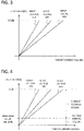
- the memory 25 stores a map data showing the relationship between the target current value and the duty ratio at each input voltage (battery voltage) as shown in FIG. 3 .
- the control section 23 preforms current control of the inductive load 13 when the target current value is large and the duty ratio is larger than a threshold value (see FIG. 4 ) and performs voltage control of the inductive load 13 when the target current value is small and the duty ratio is smaller than the threshold value, based on the relationship between the target current value and the duty ratio at each input voltage, which are stored in the memory 25. That is, when the battery voltage and the resistance of the inductive load 13 are determined, the accuracy of current is secured by voltage control.
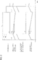
- the switching element 11 turns on/off. Specifically, the switching element 11 turns on at the timing t1, off at the timing t2, and on at the timing t3.
- the cycle T1 is a period from the timing t1 to the timing t3 and denotes one cycle.
- the on-period T2 is a period from the timing t1 to the timing t2.
- the amplifier circuit 21 amplifies the voltage V1 across the both ends of the current detecting resistor 15. Since the MOSFET 18 turns on in synchronization with the switching element 11, the charge and discharge capacitor 19 is charged with electric charge.
- the control circuit 16 detects a control circuit detecting voltage V2 having the waveform of the inclination ⁇ 2 of the time constant that is determined by the charge and discharge capacitor 19 and the discharge resistor 20.
- the voltage that the control circuit 16 detects depends on the time constant that is determined by the charge and discharge capacitor 19 and the discharge resistor 20. Therefore, the inclination of the voltage that the control circuit 16 detects does not coincide with that of the current that flows through the inductive load 13. That is, as shown in FIG. 2 , the inclination ⁇ 1 of the current that flows through the inductive load 13 does not coincide with the inclination ⁇ 2 of the control circuit detecting voltage V2 ( ⁇ 1 ⁇ 2). As a result, as the drive frequency of the switching element 11 and the duty ratio become smaller, the accuracy of current control deteriorates.
- the input voltages are 35V, 48V, and 65V.
- the input voltage is 65V.
- the input voltage becomes 35V.
- the duty ratio becomes smaller.
- the control method is shifted to voltage control such that the switching element 11 is driven at a predetermined duty ratio (fixed value).
- the threshold value is a predetermined fixed value and, for example, 10%. That is, since the time constant calculated by the reactance and the resistance of the driven inductive load is determined, the time constant can be regarded as a fixed value.
- the duty ratio is determined by the constant (reactance and resistance) of the inductive load 13 and the battery voltage VB detected by the voltage detecting circuit 22. The on/off control of the switching element 11 is performed at the duty ratio.
- the memory 25 stores the map data of the relationship between the target current value and the duty ratio that is determined based on the reactance and the resistance of the inductive load 13 at each input voltage.
- the switching method of the switching element 11 is shifted to voltage control in response to the duty ratio.
- the relationship between the target current value and the duty ratio at each input voltage may be calculated by the reactance and the resistance of the inductive load 13.
- the accuracy of the current that flows through the inductive load 13 can be improved by shifting the switching method. That is, the resistance of the inductive load 13 is measured in advance and voltage control is performed while the battery voltage is detected, so that the accuracy of the current can be secured.
- the memory 25 can store the reactance and the resistance of the inductive load 13 in advance, so that even if the specification of the inductive load 13 is changed, only the software for control may be changed without the increase of the number of the elements.
- the control section 23 When the duty ratio becomes smaller than the threshold value and the control section 23 performs voltage control of the inductive load 13, the control section 23 inputs the target current value that is the current command value and the battery voltage measured currently and calculates the duty ratio based on the battery voltage, or the voltage of the DC power supply and the target current value by the map data stored in the memory. The control section 23 returns voltage control of the inductive load 13 to current control based on the calculated duty ratio. That is, when the calculated duty ratio is larger than the threshold value, the control section 23 returns to current control of the inductive load 13.
- the apparatus for driving the inductive load, according to the present embodiment has the following advantageous effects.
- the embodiment is not limited to the above embodiment, but may be exemplified as follows.
- the MOSFET is used as the switching element 11, but is not limited to this example.
- a device such as a bipolar transistor and an IGBT may be used as the switching element 11.
- the MOSFET 18 is used in the peak hold circuit 17, but is not limited to this example.
- a diode may be used instead of the MOSFET 18.
- the peak hold circuit 17 may do without the MOSFET 18.
- the apparatus 10 is mounted on a battery-powered forklift truck, but may be mounted on any other vehicles.
Landscapes
- Engineering & Computer Science (AREA)
- Power Engineering (AREA)
- Electronic Switches (AREA)
- Dc-Dc Converters (AREA)
Claims (3)
- Vorrichtung (10) zum Betreiben einer induktiven Last (13), mit:einem Schaltelement (11), das zwischen der induktiven Last (13) und Masse in einem Stromflussweg der induktiven Last (13) bereitgestellt ist, die mit einer Gleichstromleistungsversorgung (12) verbunden ist;einer Freilaufdiode (14), die mit der induktiven Last (13) parallel schaltbar ist;einem Stromdetektionswiderstand (15), der auf einer Seite niedrigerer Spannung als die induktive Last (13) zwischen dem Schaltelement (11) und Masse in dem Stromflussweg der induktiven Last (13) bereitgestellt ist, zum Detektieren eines durch die induktive Last (13) fließenden Stroms;einer Spitzenwerthalteschaltung (17) zum Zuführen einer Spannung, die einem durch die induktive Last (13) fließenden Strom entspricht, über den Stromdetektionswiderstand (15), wenn das Schaltelement (11) ein ist, und Halten der Spannung, die über den Stromdetektionswiderstand (15) zugeführt wird, wenn das Schaltelement (11) ein ist, wenn das Schaltelement (11) aus ist;einer Spannungsdetektionsschaltung (22) zum Detektieren einer Spannung der Gleichstromleistungsversorgung (12), undeinem Steuerabschnitt (23) zum Steuern des durch die induktive Last (13) fließenden Stroms, wobei der Steuerabschnitt (23) mit dem Ausgang der Spitzenwerthalteschaltung (17) verbunden ist, und wobei der Steuerabschnitt (23) konfiguriert ist zum Durchführen einer Stromsteuerung durch Ein-/Ausschalten des Schaltelements (11) mit einem Tastverhältnis in Erwiderung auf einen Sollstromwert, während der Steuerabschnitt (23) konfiguriert ist zum Durchführen einer Regelung unter Verwendung der Ausgabe der Spitzenwerthalteschaltung (17) oder zum Durchführen einer Spannungssteuerung durch Ein-/Ausschalten des Schaltelements (11) mit einem Tastverhältnis, das basierend auf der detektierten Spannung der Gleichstromleistungsversorgung (12) und dem Sollstromwert durch eine Beziehung zwischen dem Sollstromwert und dem Tastverhältnis bei jeder Spannung der Gleichstromleistungsversorgung berechnet wird,wobei der Steuerabschnitt (23) konfiguriert ist zum Durchführen der Stromsteuerung der induktiven Last (13), wenn das Tastverhältnis größer ist als ein Schwellenwert, und zum Durchführen der Spannungssteuerung der induktiven Last (13), wenn das Tastverhältnis kleiner ist als der Schwellenwert.
- Vorrichtung (10) zum Betreiben der induktiven Last (13) gemäß Anspruch 1, wobei die Spitzenwerthalteschaltung (17) einen Lade- und Entladekondensator (19) und einen Entladewiderstand (20) umfasst.
- Vorrichtung (10) zum Betreiben der induktiven Last (13) gemäß Anspruch 1 oder 2, wobei, wenn das Tastverhältnis kleiner wird als der Schwellenwert und der Steuerabschnitt (23) eine Spannungssteuerung der induktiven Last (13) durchführt, der Steuerabschnitt (23) konfiguriert ist zum Zurückkehren zu der Stromsteuerung der induktiven Last (13), falls das Tastverhältnis, das basierend auf der detektierten Spannung der Gleichstromleistungsversorgung (12) und dem Sollstromwert berechnet wird, größer ist als der Schwellenwert.
Applications Claiming Priority (1)
| Application Number | Priority Date | Filing Date | Title |
|---|---|---|---|
| JP2017228083A JP6946976B2 (ja) | 2017-11-28 | 2017-11-28 | 誘導性負荷駆動装置 |
Publications (2)
| Publication Number | Publication Date |
|---|---|
| EP3496253A1 EP3496253A1 (de) | 2019-06-12 |
| EP3496253B1 true EP3496253B1 (de) | 2022-04-06 |
Family
ID=64267489
Family Applications (1)
| Application Number | Title | Priority Date | Filing Date |
|---|---|---|---|
| EP18204551.8A Not-in-force EP3496253B1 (de) | 2017-11-28 | 2018-11-06 | Vorrichtung zur ansteuerung einer induktiven last |
Country Status (4)
| Country | Link |
|---|---|
| US (1) | US10608627B2 (de) |
| EP (1) | EP3496253B1 (de) |
| JP (1) | JP6946976B2 (de) |
| CN (1) | CN109980904B (de) |
Families Citing this family (1)
| Publication number | Priority date | Publication date | Assignee | Title |
|---|---|---|---|---|
| US12088284B2 (en) | 2023-02-14 | 2024-09-10 | Delphi Technologies Ip Limited | Discrete relay driver circuit for peak and hold operation |
Citations (3)
| Publication number | Priority date | Publication date | Assignee | Title |
|---|---|---|---|---|
| US5214561A (en) * | 1990-11-01 | 1993-05-25 | Mitsubishi Denki Kabushiki Kaisha | Current control circuit for an electromagnetic type actuator |
| JP2013093669A (ja) * | 2011-10-24 | 2013-05-16 | Keihin Corp | 誘導性負荷駆動装置 |
| WO2017022633A1 (ja) * | 2015-08-04 | 2017-02-09 | 株式会社小糸製作所 | 車両用灯具および光源の点灯回路 |
Family Cites Families (13)
| Publication number | Priority date | Publication date | Assignee | Title |
|---|---|---|---|---|
| JPS57172705A (en) * | 1981-04-17 | 1982-10-23 | Nissan Motor Co Ltd | Solenoid drive circuit |
| JPS6441203A (en) * | 1987-08-07 | 1989-02-13 | Hitachi Ltd | Dc excitation type electromagnet device |
| JP2621453B2 (ja) * | 1988-12-29 | 1997-06-18 | 株式会社デンソー | 誘導性負荷の電流制御装置 |
| JPH07326513A (ja) * | 1994-05-31 | 1995-12-12 | Matsushita Electric Works Ltd | 電磁石駆動装置 |
| JPH09162031A (ja) * | 1995-12-13 | 1997-06-20 | Sumitomo Electric Ind Ltd | パルス幅変調方式の電流制御装置及びその電流制御方法 |
| JP2002023869A (ja) | 2000-07-06 | 2002-01-25 | Denso Corp | 誘導性負荷の通電制御装置 |
| JP4434046B2 (ja) * | 2005-03-14 | 2010-03-17 | 株式会社デンソー | 誘導性負荷制御装置 |
| US20070159143A1 (en) * | 2006-01-11 | 2007-07-12 | Ta-Yung Yang | Switching power converter with transformer arrangement |
| WO2007131947A1 (de) * | 2006-05-17 | 2007-11-22 | Continental Teves Ag & Co. Ohg | Verfahren und pulsweitenmodulierte stromregelschaltung zur ansteuerung von induktiven lasten in kraftfahrzeugen |
| JP5525405B2 (ja) * | 2010-10-01 | 2014-06-18 | 日立オートモティブシステムズ株式会社 | 電流検出回路、モータ駆動装置 |
| CN102946195B (zh) * | 2011-08-15 | 2016-04-20 | 美国亚德诺半导体公司 | 开关调节器及其控制方法 |
| CN103390991B (zh) * | 2012-05-10 | 2015-10-21 | 华润矽威科技(上海)有限公司 | 开关电源及提高其输出电流线调整率的电路 |
| US9673704B2 (en) * | 2012-10-15 | 2017-06-06 | Nxp Usa, Inc. | Inductive load control circuit, a braking system for a vehicle and a method of measuring current in an inductive load control circuit |
-
2017
- 2017-11-28 JP JP2017228083A patent/JP6946976B2/ja not_active Expired - Fee Related
-
2018
- 2018-11-06 EP EP18204551.8A patent/EP3496253B1/de not_active Not-in-force
- 2018-11-15 US US16/191,583 patent/US10608627B2/en not_active Expired - Fee Related
- 2018-11-27 CN CN201811424700.8A patent/CN109980904B/zh not_active Expired - Fee Related
Patent Citations (4)
| Publication number | Priority date | Publication date | Assignee | Title |
|---|---|---|---|---|
| US5214561A (en) * | 1990-11-01 | 1993-05-25 | Mitsubishi Denki Kabushiki Kaisha | Current control circuit for an electromagnetic type actuator |
| JP2013093669A (ja) * | 2011-10-24 | 2013-05-16 | Keihin Corp | 誘導性負荷駆動装置 |
| WO2017022633A1 (ja) * | 2015-08-04 | 2017-02-09 | 株式会社小糸製作所 | 車両用灯具および光源の点灯回路 |
| EP3334255A1 (de) * | 2015-08-04 | 2018-06-13 | Koito Manufacturing Co., Ltd. | Beleuchtungswerkzeug für fahrzeug und lichtquellenbeleuchtungsschaltung |
Also Published As
| Publication number | Publication date |
|---|---|
| CN109980904A (zh) | 2019-07-05 |
| JP2019102486A (ja) | 2019-06-24 |
| JP6946976B2 (ja) | 2021-10-13 |
| US20190165777A1 (en) | 2019-05-30 |
| US10608627B2 (en) | 2020-03-31 |
| EP3496253A1 (de) | 2019-06-12 |
| CN109980904B (zh) | 2021-05-25 |
Similar Documents
| Publication | Publication Date | Title |
|---|---|---|
| US9998004B2 (en) | Accurate non-isolated high voltage DC-DC feedback | |
| US9788370B2 (en) | Light-emitting-diode-driving device, lighting apparatus for vehicle and vehicle including the same | |
| JP4440869B2 (ja) | Dc−dcコンバータ、dc−dcコンバータの制御回路及びdc−dcコンバータの制御方法 | |
| US8625249B2 (en) | Control apparatus for electromagnetic inductive load | |
| US6650555B2 (en) | Switched-capacitor-type stabilized power circuit | |
| US20190165665A1 (en) | Voltage converting system and method of using the same | |
| KR101803539B1 (ko) | 스위치 제어 회로, 이를 포함하는 커플드 인덕터 부스트 컨버터, 및 그 구동 방법 | |
| US8089782B2 (en) | High accuracy average output current control scheme for power current converter in critical DCM | |
| US20180108825A1 (en) | Driving system for piezoelectric pump | |
| EP2424091A1 (de) | Schaltvorrichtung und verfahren zu ihrer steuerung | |
| US20150123636A1 (en) | Cuk Based Current Source | |
| US20120038335A1 (en) | Pulse modulation circuit and method | |
| US20100231184A1 (en) | Step up and down switching power converter's output current detect and control scheme | |
| EP3057233B1 (de) | Stromversorgungssteuerungsvorrichtung | |
| US9654012B2 (en) | Converter and method for controlling the same using an overcurrent protection switch | |
| EP3496253B1 (de) | Vorrichtung zur ansteuerung einer induktiven last | |
| US8836299B2 (en) | Voltage converter | |
| JP2012117589A (ja) | 電磁比例弁駆動回路 | |
| KR101981287B1 (ko) | 스위칭 레귤레이터 | |
| US9693412B2 (en) | Dimming driver circuit and control method thereof | |
| US20150016157A1 (en) | Constant switching frequency discontinuous current mode average output current control scheme | |
| US20140145671A1 (en) | Battery switching charger and method for controlling battery switching charger | |
| WO2020149084A1 (ja) | Dcdcコンバータ | |
| US20230420975A1 (en) | Power supply circuit | |
| KR20170123750A (ko) | Dc-dc 컨버터 |
Legal Events
| Date | Code | Title | Description |
|---|---|---|---|
| PUAI | Public reference made under article 153(3) epc to a published international application that has entered the european phase |
Free format text: ORIGINAL CODE: 0009012 |
|
| STAA | Information on the status of an ep patent application or granted ep patent |
Free format text: STATUS: REQUEST FOR EXAMINATION WAS MADE |
|
| 17P | Request for examination filed |
Effective date: 20181106 |
|
| AK | Designated contracting states |
Kind code of ref document: A1 Designated state(s): AL AT BE BG CH CY CZ DE DK EE ES FI FR GB GR HR HU IE IS IT LI LT LU LV MC MK MT NL NO PL PT RO RS SE SI SK SM TR |
|
| AX | Request for extension of the european patent |
Extension state: BA ME |
|
| STAA | Information on the status of an ep patent application or granted ep patent |
Free format text: STATUS: EXAMINATION IS IN PROGRESS |
|
| 17Q | First examination report despatched |
Effective date: 20200715 |
|
| GRAP | Despatch of communication of intention to grant a patent |
Free format text: ORIGINAL CODE: EPIDOSNIGR1 |
|
| STAA | Information on the status of an ep patent application or granted ep patent |
Free format text: STATUS: GRANT OF PATENT IS INTENDED |
|
| GRAJ | Information related to disapproval of communication of intention to grant by the applicant or resumption of examination proceedings by the epo deleted |
Free format text: ORIGINAL CODE: EPIDOSDIGR1 |
|
| GRAP | Despatch of communication of intention to grant a patent |
Free format text: ORIGINAL CODE: EPIDOSNIGR1 |
|
| RIC1 | Information provided on ipc code assigned before grant |
Ipc: H02M 1/00 20060101ALN20210922BHEP Ipc: H03K 7/08 20060101ALI20210922BHEP Ipc: B60T 8/36 20060101ALI20210922BHEP Ipc: H02M 3/155 20060101AFI20210922BHEP |
|
| RIC1 | Information provided on ipc code assigned before grant |
Ipc: H02M 1/00 20060101ALN20210928BHEP Ipc: H03K 7/08 20060101ALI20210928BHEP Ipc: B60T 8/36 20060101ALI20210928BHEP Ipc: H02M 3/155 20060101AFI20210928BHEP |
|
| INTG | Intention to grant announced |
Effective date: 20211012 |
|
| INTG | Intention to grant announced |
Effective date: 20211026 |
|
| GRAS | Grant fee paid |
Free format text: ORIGINAL CODE: EPIDOSNIGR3 |
|
| GRAA | (expected) grant |
Free format text: ORIGINAL CODE: 0009210 |
|
| STAA | Information on the status of an ep patent application or granted ep patent |
Free format text: STATUS: THE PATENT HAS BEEN GRANTED |
|
| AK | Designated contracting states |
Kind code of ref document: B1 Designated state(s): AL AT BE BG CH CY CZ DE DK EE ES FI FR GB GR HR HU IE IS IT LI LT LU LV MC MK MT NL NO PL PT RO RS SE SI SK SM TR |
|
| REG | Reference to a national code |
Ref country code: GB Ref legal event code: FG4D |
|
| REG | Reference to a national code |
Ref country code: CH Ref legal event code: EP |
|
| REG | Reference to a national code |
Ref country code: AT Ref legal event code: REF Ref document number: 1482316 Country of ref document: AT Kind code of ref document: T Effective date: 20220415 |
|
| REG | Reference to a national code |
Ref country code: SE Ref legal event code: TRGR |
|
| REG | Reference to a national code |
Ref country code: IE Ref legal event code: FG4D |
|
| REG | Reference to a national code |
Ref country code: DE Ref legal event code: R096 Ref document number: 602018033280 Country of ref document: DE |
|
| REG | Reference to a national code |
Ref country code: LT Ref legal event code: MG9D |
|
| REG | Reference to a national code |
Ref country code: NL Ref legal event code: MP Effective date: 20220406 |
|
| REG | Reference to a national code |
Ref country code: AT Ref legal event code: MK05 Ref document number: 1482316 Country of ref document: AT Kind code of ref document: T Effective date: 20220406 |
|
| PG25 | Lapsed in a contracting state [announced via postgrant information from national office to epo] |
Ref country code: NL Free format text: LAPSE BECAUSE OF FAILURE TO SUBMIT A TRANSLATION OF THE DESCRIPTION OR TO PAY THE FEE WITHIN THE PRESCRIBED TIME-LIMIT Effective date: 20220406 |
|
| PG25 | Lapsed in a contracting state [announced via postgrant information from national office to epo] |
Ref country code: PT Free format text: LAPSE BECAUSE OF FAILURE TO SUBMIT A TRANSLATION OF THE DESCRIPTION OR TO PAY THE FEE WITHIN THE PRESCRIBED TIME-LIMIT Effective date: 20220808 Ref country code: NO Free format text: LAPSE BECAUSE OF FAILURE TO SUBMIT A TRANSLATION OF THE DESCRIPTION OR TO PAY THE FEE WITHIN THE PRESCRIBED TIME-LIMIT Effective date: 20220706 Ref country code: LT Free format text: LAPSE BECAUSE OF FAILURE TO SUBMIT A TRANSLATION OF THE DESCRIPTION OR TO PAY THE FEE WITHIN THE PRESCRIBED TIME-LIMIT Effective date: 20220406 Ref country code: HR Free format text: LAPSE BECAUSE OF FAILURE TO SUBMIT A TRANSLATION OF THE DESCRIPTION OR TO PAY THE FEE WITHIN THE PRESCRIBED TIME-LIMIT Effective date: 20220406 Ref country code: GR Free format text: LAPSE BECAUSE OF FAILURE TO SUBMIT A TRANSLATION OF THE DESCRIPTION OR TO PAY THE FEE WITHIN THE PRESCRIBED TIME-LIMIT Effective date: 20220707 Ref country code: FI Free format text: LAPSE BECAUSE OF FAILURE TO SUBMIT A TRANSLATION OF THE DESCRIPTION OR TO PAY THE FEE WITHIN THE PRESCRIBED TIME-LIMIT Effective date: 20220406 Ref country code: ES Free format text: LAPSE BECAUSE OF FAILURE TO SUBMIT A TRANSLATION OF THE DESCRIPTION OR TO PAY THE FEE WITHIN THE PRESCRIBED TIME-LIMIT Effective date: 20220406 Ref country code: BG Free format text: LAPSE BECAUSE OF FAILURE TO SUBMIT A TRANSLATION OF THE DESCRIPTION OR TO PAY THE FEE WITHIN THE PRESCRIBED TIME-LIMIT Effective date: 20220706 Ref country code: AT Free format text: LAPSE BECAUSE OF FAILURE TO SUBMIT A TRANSLATION OF THE DESCRIPTION OR TO PAY THE FEE WITHIN THE PRESCRIBED TIME-LIMIT Effective date: 20220406 |
|
| PG25 | Lapsed in a contracting state [announced via postgrant information from national office to epo] |
Ref country code: RS Free format text: LAPSE BECAUSE OF FAILURE TO SUBMIT A TRANSLATION OF THE DESCRIPTION OR TO PAY THE FEE WITHIN THE PRESCRIBED TIME-LIMIT Effective date: 20220406 Ref country code: PL Free format text: LAPSE BECAUSE OF FAILURE TO SUBMIT A TRANSLATION OF THE DESCRIPTION OR TO PAY THE FEE WITHIN THE PRESCRIBED TIME-LIMIT Effective date: 20220406 Ref country code: LV Free format text: LAPSE BECAUSE OF FAILURE TO SUBMIT A TRANSLATION OF THE DESCRIPTION OR TO PAY THE FEE WITHIN THE PRESCRIBED TIME-LIMIT Effective date: 20220406 Ref country code: IS Free format text: LAPSE BECAUSE OF FAILURE TO SUBMIT A TRANSLATION OF THE DESCRIPTION OR TO PAY THE FEE WITHIN THE PRESCRIBED TIME-LIMIT Effective date: 20220806 |
|
| REG | Reference to a national code |
Ref country code: DE Ref legal event code: R097 Ref document number: 602018033280 Country of ref document: DE |
|
| PG25 | Lapsed in a contracting state [announced via postgrant information from national office to epo] |
Ref country code: SM Free format text: LAPSE BECAUSE OF FAILURE TO SUBMIT A TRANSLATION OF THE DESCRIPTION OR TO PAY THE FEE WITHIN THE PRESCRIBED TIME-LIMIT Effective date: 20220406 Ref country code: SK Free format text: LAPSE BECAUSE OF FAILURE TO SUBMIT A TRANSLATION OF THE DESCRIPTION OR TO PAY THE FEE WITHIN THE PRESCRIBED TIME-LIMIT Effective date: 20220406 Ref country code: RO Free format text: LAPSE BECAUSE OF FAILURE TO SUBMIT A TRANSLATION OF THE DESCRIPTION OR TO PAY THE FEE WITHIN THE PRESCRIBED TIME-LIMIT Effective date: 20220406 Ref country code: EE Free format text: LAPSE BECAUSE OF FAILURE TO SUBMIT A TRANSLATION OF THE DESCRIPTION OR TO PAY THE FEE WITHIN THE PRESCRIBED TIME-LIMIT Effective date: 20220406 Ref country code: DK Free format text: LAPSE BECAUSE OF FAILURE TO SUBMIT A TRANSLATION OF THE DESCRIPTION OR TO PAY THE FEE WITHIN THE PRESCRIBED TIME-LIMIT Effective date: 20220406 Ref country code: CZ Free format text: LAPSE BECAUSE OF FAILURE TO SUBMIT A TRANSLATION OF THE DESCRIPTION OR TO PAY THE FEE WITHIN THE PRESCRIBED TIME-LIMIT Effective date: 20220406 |
|
| PGFP | Annual fee paid to national office [announced via postgrant information from national office to epo] |
Ref country code: SE Payment date: 20221011 Year of fee payment: 5 Ref country code: IT Payment date: 20221011 Year of fee payment: 5 Ref country code: DE Payment date: 20220930 Year of fee payment: 5 |
|
| PLBE | No opposition filed within time limit |
Free format text: ORIGINAL CODE: 0009261 |
|
| STAA | Information on the status of an ep patent application or granted ep patent |
Free format text: STATUS: NO OPPOSITION FILED WITHIN TIME LIMIT |
|
| 26N | No opposition filed |
Effective date: 20230110 |
|
| PG25 | Lapsed in a contracting state [announced via postgrant information from national office to epo] |
Ref country code: AL Free format text: LAPSE BECAUSE OF FAILURE TO SUBMIT A TRANSLATION OF THE DESCRIPTION OR TO PAY THE FEE WITHIN THE PRESCRIBED TIME-LIMIT Effective date: 20220406 |
|
| PG25 | Lapsed in a contracting state [announced via postgrant information from national office to epo] |
Ref country code: SI Free format text: LAPSE BECAUSE OF FAILURE TO SUBMIT A TRANSLATION OF THE DESCRIPTION OR TO PAY THE FEE WITHIN THE PRESCRIBED TIME-LIMIT Effective date: 20220406 |
|
| PG25 | Lapsed in a contracting state [announced via postgrant information from national office to epo] |
Ref country code: MC Free format text: LAPSE BECAUSE OF FAILURE TO SUBMIT A TRANSLATION OF THE DESCRIPTION OR TO PAY THE FEE WITHIN THE PRESCRIBED TIME-LIMIT Effective date: 20220406 |
|
| REG | Reference to a national code |
Ref country code: CH Ref legal event code: PL |
|
| GBPC | Gb: european patent ceased through non-payment of renewal fee |
Effective date: 20221106 |
|
| REG | Reference to a national code |
Ref country code: BE Ref legal event code: MM Effective date: 20221130 |
|
| PG25 | Lapsed in a contracting state [announced via postgrant information from national office to epo] |
Ref country code: LI Free format text: LAPSE BECAUSE OF NON-PAYMENT OF DUE FEES Effective date: 20221130 Ref country code: CH Free format text: LAPSE BECAUSE OF NON-PAYMENT OF DUE FEES Effective date: 20221130 |
|
| PG25 | Lapsed in a contracting state [announced via postgrant information from national office to epo] |
Ref country code: LU Free format text: LAPSE BECAUSE OF NON-PAYMENT OF DUE FEES Effective date: 20221106 |
|
| PG25 | Lapsed in a contracting state [announced via postgrant information from national office to epo] |
Ref country code: IE Free format text: LAPSE BECAUSE OF NON-PAYMENT OF DUE FEES Effective date: 20221106 Ref country code: GB Free format text: LAPSE BECAUSE OF NON-PAYMENT OF DUE FEES Effective date: 20221106 |
|
| PG25 | Lapsed in a contracting state [announced via postgrant information from national office to epo] |
Ref country code: FR Free format text: LAPSE BECAUSE OF NON-PAYMENT OF DUE FEES Effective date: 20221130 Ref country code: BE Free format text: LAPSE BECAUSE OF NON-PAYMENT OF DUE FEES Effective date: 20221130 |
|
| PG25 | Lapsed in a contracting state [announced via postgrant information from national office to epo] |
Ref country code: HU Free format text: LAPSE BECAUSE OF FAILURE TO SUBMIT A TRANSLATION OF THE DESCRIPTION OR TO PAY THE FEE WITHIN THE PRESCRIBED TIME-LIMIT; INVALID AB INITIO Effective date: 20181106 |
|
| PG25 | Lapsed in a contracting state [announced via postgrant information from national office to epo] |
Ref country code: CY Free format text: LAPSE BECAUSE OF FAILURE TO SUBMIT A TRANSLATION OF THE DESCRIPTION OR TO PAY THE FEE WITHIN THE PRESCRIBED TIME-LIMIT Effective date: 20220406 |
|
| PG25 | Lapsed in a contracting state [announced via postgrant information from national office to epo] |
Ref country code: MK Free format text: LAPSE BECAUSE OF FAILURE TO SUBMIT A TRANSLATION OF THE DESCRIPTION OR TO PAY THE FEE WITHIN THE PRESCRIBED TIME-LIMIT Effective date: 20220406 |
|
| REG | Reference to a national code |
Ref country code: DE Ref legal event code: R119 Ref document number: 602018033280 Country of ref document: DE |
|
| REG | Reference to a national code |
Ref country code: SE Ref legal event code: EUG |
|
| PG25 | Lapsed in a contracting state [announced via postgrant information from national office to epo] |
Ref country code: SE Free format text: LAPSE BECAUSE OF NON-PAYMENT OF DUE FEES Effective date: 20231107 |
|
| PG25 | Lapsed in a contracting state [announced via postgrant information from national office to epo] |
Ref country code: MT Free format text: LAPSE BECAUSE OF FAILURE TO SUBMIT A TRANSLATION OF THE DESCRIPTION OR TO PAY THE FEE WITHIN THE PRESCRIBED TIME-LIMIT Effective date: 20220406 |
|
| PG25 | Lapsed in a contracting state [announced via postgrant information from national office to epo] |
Ref country code: DE Free format text: LAPSE BECAUSE OF NON-PAYMENT OF DUE FEES Effective date: 20240601 |
|
| PG25 | Lapsed in a contracting state [announced via postgrant information from national office to epo] |
Ref country code: DE Free format text: LAPSE BECAUSE OF NON-PAYMENT OF DUE FEES Effective date: 20240601 |
|
| PG25 | Lapsed in a contracting state [announced via postgrant information from national office to epo] |
Ref country code: BG Free format text: LAPSE BECAUSE OF FAILURE TO SUBMIT A TRANSLATION OF THE DESCRIPTION OR TO PAY THE FEE WITHIN THE PRESCRIBED TIME-LIMIT Effective date: 20220406 |
|
| PG25 | Lapsed in a contracting state [announced via postgrant information from national office to epo] |
Ref country code: BG Free format text: LAPSE BECAUSE OF FAILURE TO SUBMIT A TRANSLATION OF THE DESCRIPTION OR TO PAY THE FEE WITHIN THE PRESCRIBED TIME-LIMIT Effective date: 20220406 |
|
| PG25 | Lapsed in a contracting state [announced via postgrant information from national office to epo] |
Ref country code: IT Free format text: LAPSE BECAUSE OF NON-PAYMENT OF DUE FEES Effective date: 20231106 |
|
| PG25 | Lapsed in a contracting state [announced via postgrant information from national office to epo] |
Ref country code: IT Free format text: LAPSE BECAUSE OF NON-PAYMENT OF DUE FEES Effective date: 20231106 |
|
| PG25 | Lapsed in a contracting state [announced via postgrant information from national office to epo] |
Ref country code: TR Free format text: LAPSE BECAUSE OF FAILURE TO SUBMIT A TRANSLATION OF THE DESCRIPTION OR TO PAY THE FEE WITHIN THE PRESCRIBED TIME-LIMIT Effective date: 20220406 |