EP3499557A1 - Procédés pour vias auto-alignés gravés sélectivement - Google Patents
Procédés pour vias auto-alignés gravés sélectivement Download PDFInfo
- Publication number
- EP3499557A1 EP3499557A1 EP18211015.5A EP18211015A EP3499557A1 EP 3499557 A1 EP3499557 A1 EP 3499557A1 EP 18211015 A EP18211015 A EP 18211015A EP 3499557 A1 EP3499557 A1 EP 3499557A1
- Authority
- EP
- European Patent Office
- Prior art keywords
- insulating layer
- hardmask
- opening
- layer
- conductive
- Prior art date
- Legal status (The legal status is an assumption and is not a legal conclusion. Google has not performed a legal analysis and makes no representation as to the accuracy of the status listed.)
- Withdrawn
Links
Images






Classifications
-
- H—ELECTRICITY
- H10—SEMICONDUCTOR DEVICES; ELECTRIC SOLID-STATE DEVICES NOT OTHERWISE PROVIDED FOR
- H10W—GENERIC PACKAGES, INTERCONNECTIONS, CONNECTORS OR OTHER CONSTRUCTIONAL DETAILS OF DEVICES COVERED BY CLASS H10
- H10W20/00—Interconnections in chips, wafers or substrates
- H10W20/01—Manufacture or treatment
- H10W20/071—Manufacture or treatment of dielectric parts thereof
- H10W20/081—Manufacture or treatment of dielectric parts thereof by forming openings in the dielectric parts
-
- H—ELECTRICITY
- H10—SEMICONDUCTOR DEVICES; ELECTRIC SOLID-STATE DEVICES NOT OTHERWISE PROVIDED FOR
- H10W—GENERIC PACKAGES, INTERCONNECTIONS, CONNECTORS OR OTHER CONSTRUCTIONAL DETAILS OF DEVICES COVERED BY CLASS H10
- H10W20/00—Interconnections in chips, wafers or substrates
- H10W20/01—Manufacture or treatment
- H10W20/071—Manufacture or treatment of dielectric parts thereof
- H10W20/081—Manufacture or treatment of dielectric parts thereof by forming openings in the dielectric parts
- H10W20/089—Manufacture or treatment of dielectric parts thereof by forming openings in the dielectric parts using processes for implementing desired shapes or dispositions of the openings, e.g. double patterning
-
- H—ELECTRICITY
- H10—SEMICONDUCTOR DEVICES; ELECTRIC SOLID-STATE DEVICES NOT OTHERWISE PROVIDED FOR
- H10P—GENERIC PROCESSES OR APPARATUS FOR THE MANUFACTURE OR TREATMENT OF DEVICES COVERED BY CLASS H10
- H10P14/00—Formation of materials, e.g. in the shape of layers or pillars
- H10P14/40—Formation of materials, e.g. in the shape of layers or pillars of conductive or resistive materials
-
- H—ELECTRICITY
- H10—SEMICONDUCTOR DEVICES; ELECTRIC SOLID-STATE DEVICES NOT OTHERWISE PROVIDED FOR
- H10P—GENERIC PROCESSES OR APPARATUS FOR THE MANUFACTURE OR TREATMENT OF DEVICES COVERED BY CLASS H10
- H10P50/00—Etching of wafers, substrates or parts of devices
- H10P50/20—Dry etching; Plasma etching; Reactive-ion etching
- H10P50/28—Dry etching; Plasma etching; Reactive-ion etching of insulating materials
- H10P50/282—Dry etching; Plasma etching; Reactive-ion etching of insulating materials of inorganic materials
-
- H—ELECTRICITY
- H10—SEMICONDUCTOR DEVICES; ELECTRIC SOLID-STATE DEVICES NOT OTHERWISE PROVIDED FOR
- H10P—GENERIC PROCESSES OR APPARATUS FOR THE MANUFACTURE OR TREATMENT OF DEVICES COVERED BY CLASS H10
- H10P76/00—Manufacture or treatment of masks on semiconductor bodies, e.g. by lithography or photolithography
- H10P76/40—Manufacture or treatment of masks on semiconductor bodies, e.g. by lithography or photolithography of masks comprising inorganic materials
- H10P76/408—Manufacture or treatment of masks on semiconductor bodies, e.g. by lithography or photolithography of masks comprising inorganic materials characterised by their sizes, orientations, dispositions, behaviours or shapes
- H10P76/4085—Manufacture or treatment of masks on semiconductor bodies, e.g. by lithography or photolithography of masks comprising inorganic materials characterised by their sizes, orientations, dispositions, behaviours or shapes characterised by the processes involved to create the masks
-
- H—ELECTRICITY
- H10—SEMICONDUCTOR DEVICES; ELECTRIC SOLID-STATE DEVICES NOT OTHERWISE PROVIDED FOR
- H10W—GENERIC PACKAGES, INTERCONNECTIONS, CONNECTORS OR OTHER CONSTRUCTIONAL DETAILS OF DEVICES COVERED BY CLASS H10
- H10W20/00—Interconnections in chips, wafers or substrates
- H10W20/01—Manufacture or treatment
- H10W20/031—Manufacture or treatment of conductive parts of the interconnections
- H10W20/056—Manufacture or treatment of conductive parts of the interconnections by filling conductive material into holes, grooves or trenches
-
- H—ELECTRICITY
- H10—SEMICONDUCTOR DEVICES; ELECTRIC SOLID-STATE DEVICES NOT OTHERWISE PROVIDED FOR
- H10W—GENERIC PACKAGES, INTERCONNECTIONS, CONNECTORS OR OTHER CONSTRUCTIONAL DETAILS OF DEVICES COVERED BY CLASS H10
- H10W20/00—Interconnections in chips, wafers or substrates
- H10W20/01—Manufacture or treatment
- H10W20/031—Manufacture or treatment of conductive parts of the interconnections
- H10W20/069—Manufacture or treatment of conductive parts of the interconnections by forming self-aligned vias or self-aligned contact plugs
-
- H—ELECTRICITY
- H10—SEMICONDUCTOR DEVICES; ELECTRIC SOLID-STATE DEVICES NOT OTHERWISE PROVIDED FOR
- H10W—GENERIC PACKAGES, INTERCONNECTIONS, CONNECTORS OR OTHER CONSTRUCTIONAL DETAILS OF DEVICES COVERED BY CLASS H10
- H10W20/00—Interconnections in chips, wafers or substrates
- H10W20/01—Manufacture or treatment
- H10W20/031—Manufacture or treatment of conductive parts of the interconnections
- H10W20/069—Manufacture or treatment of conductive parts of the interconnections by forming self-aligned vias or self-aligned contact plugs
- H10W20/0693—Manufacture or treatment of conductive parts of the interconnections by forming self-aligned vias or self-aligned contact plugs by forming self-aligned vias
-
- H—ELECTRICITY
- H10—SEMICONDUCTOR DEVICES; ELECTRIC SOLID-STATE DEVICES NOT OTHERWISE PROVIDED FOR
- H10W—GENERIC PACKAGES, INTERCONNECTIONS, CONNECTORS OR OTHER CONSTRUCTIONAL DETAILS OF DEVICES COVERED BY CLASS H10
- H10W20/00—Interconnections in chips, wafers or substrates
- H10W20/01—Manufacture or treatment
- H10W20/071—Manufacture or treatment of dielectric parts thereof
- H10W20/074—Manufacture or treatment of dielectric parts thereof of dielectric parts comprising thin functional dielectric layers, e.g. dielectric etch-stop, barrier, capping or liner layers
-
- H—ELECTRICITY
- H10—SEMICONDUCTOR DEVICES; ELECTRIC SOLID-STATE DEVICES NOT OTHERWISE PROVIDED FOR
- H10W—GENERIC PACKAGES, INTERCONNECTIONS, CONNECTORS OR OTHER CONSTRUCTIONAL DETAILS OF DEVICES COVERED BY CLASS H10
- H10W20/00—Interconnections in chips, wafers or substrates
- H10W20/01—Manufacture or treatment
- H10W20/071—Manufacture or treatment of dielectric parts thereof
- H10W20/074—Manufacture or treatment of dielectric parts thereof of dielectric parts comprising thin functional dielectric layers, e.g. dielectric etch-stop, barrier, capping or liner layers
- H10W20/076—Manufacture or treatment of dielectric parts thereof of dielectric parts comprising thin functional dielectric layers, e.g. dielectric etch-stop, barrier, capping or liner layers in via holes or trenches
-
- H—ELECTRICITY
- H10—SEMICONDUCTOR DEVICES; ELECTRIC SOLID-STATE DEVICES NOT OTHERWISE PROVIDED FOR
- H10W—GENERIC PACKAGES, INTERCONNECTIONS, CONNECTORS OR OTHER CONSTRUCTIONAL DETAILS OF DEVICES COVERED BY CLASS H10
- H10W20/00—Interconnections in chips, wafers or substrates
- H10W20/01—Manufacture or treatment
- H10W20/071—Manufacture or treatment of dielectric parts thereof
- H10W20/081—Manufacture or treatment of dielectric parts thereof by forming openings in the dielectric parts
- H10W20/083—Manufacture or treatment of dielectric parts thereof by forming openings in the dielectric parts the openings being via holes penetrating underlying conductors
-
- H—ELECTRICITY
- H10—SEMICONDUCTOR DEVICES; ELECTRIC SOLID-STATE DEVICES NOT OTHERWISE PROVIDED FOR
- H10W—GENERIC PACKAGES, INTERCONNECTIONS, CONNECTORS OR OTHER CONSTRUCTIONAL DETAILS OF DEVICES COVERED BY CLASS H10
- H10W20/00—Interconnections in chips, wafers or substrates
- H10W20/01—Manufacture or treatment
- H10W20/071—Manufacture or treatment of dielectric parts thereof
- H10W20/081—Manufacture or treatment of dielectric parts thereof by forming openings in the dielectric parts
- H10W20/084—Manufacture or treatment of dielectric parts thereof by forming openings in the dielectric parts for dual-damascene structures
- H10W20/085—Manufacture or treatment of dielectric parts thereof by forming openings in the dielectric parts for dual-damascene structures involving intermediate temporary filling with material
-
- H—ELECTRICITY
- H10—SEMICONDUCTOR DEVICES; ELECTRIC SOLID-STATE DEVICES NOT OTHERWISE PROVIDED FOR
- H10W—GENERIC PACKAGES, INTERCONNECTIONS, CONNECTORS OR OTHER CONSTRUCTIONAL DETAILS OF DEVICES COVERED BY CLASS H10
- H10W20/00—Interconnections in chips, wafers or substrates
- H10W20/01—Manufacture or treatment
- H10W20/071—Manufacture or treatment of dielectric parts thereof
- H10W20/081—Manufacture or treatment of dielectric parts thereof by forming openings in the dielectric parts
- H10W20/084—Manufacture or treatment of dielectric parts thereof by forming openings in the dielectric parts for dual-damascene structures
- H10W20/087—Manufacture or treatment of dielectric parts thereof by forming openings in the dielectric parts for dual-damascene structures involving multiple stacked pre-patterned masks
-
- H—ELECTRICITY
- H10—SEMICONDUCTOR DEVICES; ELECTRIC SOLID-STATE DEVICES NOT OTHERWISE PROVIDED FOR
- H10P—GENERIC PROCESSES OR APPARATUS FOR THE MANUFACTURE OR TREATMENT OF DEVICES COVERED BY CLASS H10
- H10P50/00—Etching of wafers, substrates or parts of devices
- H10P50/73—Etching of wafers, substrates or parts of devices using masks for insulating materials
-
- H—ELECTRICITY
- H10—SEMICONDUCTOR DEVICES; ELECTRIC SOLID-STATE DEVICES NOT OTHERWISE PROVIDED FOR
- H10W—GENERIC PACKAGES, INTERCONNECTIONS, CONNECTORS OR OTHER CONSTRUCTIONAL DETAILS OF DEVICES COVERED BY CLASS H10
- H10W20/00—Interconnections in chips, wafers or substrates
- H10W20/01—Manufacture or treatment
- H10W20/071—Manufacture or treatment of dielectric parts thereof
- H10W20/074—Manufacture or treatment of dielectric parts thereof of dielectric parts comprising thin functional dielectric layers, e.g. dielectric etch-stop, barrier, capping or liner layers
- H10W20/077—Manufacture or treatment of dielectric parts thereof of dielectric parts comprising thin functional dielectric layers, e.g. dielectric etch-stop, barrier, capping or liner layers on sidewalls or on top surfaces of conductors
-
- H—ELECTRICITY
- H10—SEMICONDUCTOR DEVICES; ELECTRIC SOLID-STATE DEVICES NOT OTHERWISE PROVIDED FOR
- H10W—GENERIC PACKAGES, INTERCONNECTIONS, CONNECTORS OR OTHER CONSTRUCTIONAL DETAILS OF DEVICES COVERED BY CLASS H10
- H10W20/00—Interconnections in chips, wafers or substrates
- H10W20/01—Manufacture or treatment
- H10W20/071—Manufacture or treatment of dielectric parts thereof
- H10W20/081—Manufacture or treatment of dielectric parts thereof by forming openings in the dielectric parts
- H10W20/084—Manufacture or treatment of dielectric parts thereof by forming openings in the dielectric parts for dual-damascene structures
- H10W20/0886—Manufacture or treatment of dielectric parts thereof by forming openings in the dielectric parts for dual-damascene structures involving forming a via in a via-level dielectric prior to deposition of a trench-level dielectric
-
- H—ELECTRICITY
- H10—SEMICONDUCTOR DEVICES; ELECTRIC SOLID-STATE DEVICES NOT OTHERWISE PROVIDED FOR
- H10W—GENERIC PACKAGES, INTERCONNECTIONS, CONNECTORS OR OTHER CONSTRUCTIONAL DETAILS OF DEVICES COVERED BY CLASS H10
- H10W20/00—Interconnections in chips, wafers or substrates
- H10W20/01—Manufacture or treatment
- H10W20/071—Manufacture or treatment of dielectric parts thereof
- H10W20/081—Manufacture or treatment of dielectric parts thereof by forming openings in the dielectric parts
- H10W20/084—Manufacture or treatment of dielectric parts thereof by forming openings in the dielectric parts for dual-damascene structures
- H10W20/0888—Manufacture or treatment of dielectric parts thereof by forming openings in the dielectric parts for dual-damascene structures wherein via-level dielectrics are compositionally different than trench-level dielectrics
Definitions
- Embodiments of the present disclosure pertain to the field of electronic device manufacturing, and in particular, to an integrated circuit (IC) manufacturing.
- IC integrated circuit
- an integrated circuit refers to a set of electronic devices, e.g., transistors formed on a small chip of semiconductor material, typically, silicon.
- the IC includes one or more layers of metallization having metal lines to connect the electronic devices of the IC to one another and to external connections.
- layers of the interlayer dielectric material arc placed between the metallization layers of the IC for insulation.
- an interconnect structure typically, to manufacture an interconnect structure, a planar process is used that involves aligning and connecting one layer of metallization to another layer of metallization.
- patterning of the metal lines in the metallization layer is performed independently from the vias above that metallization layer.
- Conventional via manufacturing techniques cannot provide the full via self-alignment.
- the vias formed to connect lines in an upper metallization layer to a lower metallization are often misaligned.
- the via-line misalignment increases via resistance and leads to potential shorting to the wrong metal line.
- the via-line misalignment causes device failures, decreases yield and increases manufacturing cost.
- One or more embodiments of the disclosure are directed to methods to provide self-aligned vias.
- First conductive lines are recessed on a first insulating layer on a substrate.
- the first conductive lines extend along a first direction on the first insulating layer.
- a second insulating layer is deposited on the first insulating layer and the recessed first conductive lines.
- a hardmask is formed on the second insulating layer.
- the hardmask has a first opening aligned with one of the first conductive lines.
- a photoresist is formed on the hardmask.
- the photoresist has a second opening aligned with the first opening.
- the second insulating layer is partially etched to a depth through the second opening.
- the photoresist is removed to leave the hardmask with the first opening.
- the second insulating layer is etched through the first opening to form a via.
- Additional embodiments of the disclosure are directed to methods of forming self-aligned vias.
- a substrate comprising a first insulating layer with a plurality of first conductive lines extending in a first direction is provided.
- the first conductive lines are recessed so that a top surface of the first conductive lines is a recess depth below a top surface of the first insulating layer.
- a conformal liner is deposited on the recessed first conductive lines and the first insulating layer.
- a second insulating layer is deposited on the liner on the first insulating layer and the recessed first conductive lines.
- a hardmask is formed on the second insulating layer. The hardmask has a first opening aligned with one of the first conductive lines.
- a photoresist with a second opening aligned with the first opening is formed on the hardmask.
- the second insulating layer is partially etched to a depth through the second opening.
- the photoresist is removed to leave the hardmask with the first opening.
- the second insulating layer is etched through the first opening to expose the liner in the recessed first conductive line.
- the liner in the first conductive line is removed to form a via.
- a substrate comprising a first insulating layer with a plurality of first conductive lines extending in a first direction is provided.
- the first conductive lines are recessed so that a top surface of the first conductive lines is a recess depth below a top surface of the first insulating layer.
- a second insulating layer is deposited directly on the first insulating layer and the recessed first conductive lines.
- a hardmask is formed on the second insulating layer.
- the hardmask has a first opening aligned with one of the first conductive lines.
- a photoresist is formed on the hardmask.
- the photoresist has a second opening aligned with the first opening.
- the second insulating layer is partially etched to a depth through the second opening.
- the photoresist is removed to leave the hardmask with the first opening.
- the second insulating layer is etched through the first opening to expose the first conductive line to form a via.
- a “substrate” as used herein, refers to any substrate or material surface formed on a substrate upon which film processing is performed during a fabrication process.
- a substrate surface on which processing can be performed include materials such as silicon, silicon oxide, strained silicon, silicon on insulator (SOI), carbon doped silicon oxides, amorphous silicon, doped silicon, germanium, gallium arsenide, glass, sapphire, and any other materials such as metals, metal nitrides, metal alloys, and other conductive materials, depending on the application.
- Substrates include, without limitation, semiconductor wafers. Substrates may be exposed to a pretreatment process to polish, etch, reduce, oxidize, hydroxylate, anneal and/or bake the substrate surface.
- any of the film processing steps disclosed may also be performed on an under-layer formed on the substrate as disclosed in more detail below, and the term "substrate surface" is intended to include such under-layer as the context indicates.
- substrate surface is intended to include such under-layer as the context indicates.
- the terms "precursor”, “reactant”, “reactive gas” and the like are used interchangeably to refer to any gaseous species that can react with the substrate surface.
- a first metallization layer comprising a set of first conductive lines extending along a first direction on a first insulating layer on a substrate is formed.
- a second insulating layer is formed on the first insulating layer.
- a second metallization layer comprising a set of second conductive lines on the second insulating layer above the first metallization layer is formed.
- the set of second conductive lines extend along a second direction.
- a via is formed between the first metallization layer and the second metallization layer. The via is self-aligned along the second direction to one of the first conductive lines.
- the via is self-aligned along the first direction to one of the second conductive lines, as described in further detail below.
- first and second directions cross each other at an angle. In some embodiments, the first direction and second direction are substantially orthogonal to each other. In some embodiments, a fully self-aligned via is a via that is self-aligned along at least two directions to the conductive lines in a lower and an upper metallization layer.
- Methods of forming a self-aligned via comprising recessing a first metallization layer comprising a set of first conductive lines that extend along a first direction on a first insulating layer on a substrate are described.
- a second insulating layer is formed on the first insulating layer.
- a via is formed through the second insulating layer to one of the first conductive lines.
- Semiconductor devices comprising the self-aligned via and apparatus for forming the self-aligned via are also disclosed.
- One or more embodiments of the disclosure advantageously eliminate the via misalignment issues and avoid electrically shorting to the wrong metal line.
- the fully self-aligned vias provide lower via resistance and capacitance benefits over the conventional vias.
- Embodiments of the self-aligned vias provide full alignment between the vias and the conductive lines of the metallization layers that are substantially error free and advantageously increase the device yield and/or reduce the device cost.
- FIGS. 1A through 24B Exemplary processes according to one or more embodiments of the disclosure are illustrated in FIGS. 1A through 24B .
- Each of the Figures is split into an A illustration (e.g., FIG. 1A ) and a B illustration (e.g., FIG. 1B ).
- the A illustration for each Figure is a side view of a portion of a device.
- the B illustration is a top view of the portion of the device shown in the corresponding A illustration showing a cross-section line A-A' upon which the A illustration is shown.
- FIGS. 1A and 1B illustrate a cross-sectional view 100 and a top view 110, respectively, of an electronic device structure to provide a fully self-aligned via according to one or more embodiment of the disclosure.
- the cross-sectional view 110 is along an axis A-A', as depicted in Figure 1A .
- a lower metallization layer (Mx) comprises a set of first conductive lines 103 that extend along an X axis (direction) 121 on a first insulating layer 102 on a substrate 101, as shown in Figures 1A and 1B .
- X axis (direction) 121 crosses Y axis (direction) 122 at an angle 123.
- angle 123 is about 90 degrees. In another embodiment, angle 123 is an angle that is other than a 90-degree angle.
- the coordinate axis shown in FIG. 1A is representative of the coordinate axis for each of the A illustrations.
- the coordinate axis shown in FIG. 1B is representative of the coordinate axis for each of the B illustrations.
- the coordinate axis of FIG. 1A illustrates the Y axis (direction 122) and the Z axis (direction 124). Components displaced along the Z axis (direction 124) may be referred to as being above or below, or similar. However, this is merely for descriptive purposes and the skilled artisan will recognize that the electronic device structure can be in any orientation.
- the first insulating layer 102 comprises trenches 104.
- the trenches 104 have bottoms and sidewalls. The bottoms and sidewalls are bounded by the first insulating layer 102.
- the first conductive lines 103 are deposited in trenches 104 formed in the first insulating layer 102.
- the substrate 101 comprises a semiconductor material, e.g., silicon (Si), carbon (C), germanium (Ge), silicon germanium (SiGe), gallium arsenide (GaAs), InP, GaAs, InGaAs, InAIAs, other semiconductor material, or any combination thereof.
- substrate 101 is a semiconductor-on-isolator (SOI) substrate including a bulk lower substrate, a middle insulation layer, and a top monocrystalline layer.
- the top monocrystalline layer may comprise any material listed above, e.g., silicon.
- the substrate can be, e.g., an organic.
- any material that may serve as a foundation upon which passive and active electronic devices e.g., transistors, memories, capacitors, inductors, resistors, switches, integrated circuits, amplifiers, optoelectronic devices, or any other electronic devices
- passive and active electronic devices e.g., transistors, memories, capacitors, inductors, resistors, switches, integrated circuits, amplifiers, optoelectronic devices, or any other electronic devices
- substrate 101 includes one or more metallization interconnect layers for integrated circuits.
- the substrate 101 includes interconnects, for example, vias, configured to connect the metallization layers.
- the substrate 101 includes electronic devices, e.g., transistors, memories, capacitors, resistors, optoelectronic devices, switches, and any other active and passive electronic devices that are separated by an electrically insulating layer, for example, an interlayer dielectric, a trench insulation layer, or any other insulating layer known to one of ordinary skill in the art of the electronic device manufacturing.
- the substrate includes one or more buffer layers to accommodate for a lattice mismatch between the substrate 101 and one or more layers above substrate 101 and to confine lattice dislocations and defects.
- First insulating layer 102 can be any material suitable to insulate adjacent devices and prevent leakage.
- electrically insulating layer 102 is an oxide layer, e.g., silicon dioxide, or any other electrically insulating layer determined by an electronic device design.
- first insulating layer 102 comprises an interlayer dielectric (ILD).
- first insulating layer 102 is a low-k dielectric that includes, but is not limited to, materials such as, e.g., silicon dioxide, silicon oxide, carbon doped oxide ("CDO"), e.g., carbon doped silicon dioxide, porous silicon dioxide, silicon nitride, or any combination thereof.
- first insulating layer 102 includes a dielectric material having a k-value less than 5. In some embodiments, first insulating layer 102 includes a dielectric material having a k-value less than 2. In some embodiments, first insulating layer 102 includes a nitride, oxide, a polymer, phosphosilicate glass, fluourosilicate (SiOF) glass, organosilicate glass (SiOCH), other electrically insulating layer determined by an electronic device design, or any combination thereof. In some embodiments, first insulating layer 102 may include polyimide, epoxy, photodefinable materials, such as benzocyclobutene (BCB), and WPR-series materials, or spin-on-glass.
- BCB benzocyclobutene
- first insulating layer 102 is a low-k interlayer dielectric to isolate one metal line from other metal lines on substrate 101. In some embodiments, the thickness of the first insulating layer 102 is in an approximate range from about 10 nanometers (nm) to about 2 microns ( ⁇ m).
- first insulating layer 102 is deposited using one of deposition techniques, such as but not limited to a chemical vapor deposition (“CVD”), a physical vapor deposition (“PVD”), molecular beam epitaxy (“MBE”), metalorganic chemical vapor deposition (“MOCVD”), atomic layer deposition (“ALD”), spin-on, or other insulating deposition techniques known to one of ordinary skill in the art of microelectronic device manufacturing.
- CVD chemical vapor deposition
- PVD physical vapor deposition
- MBE molecular beam epitaxy
- MOCVD metalorganic chemical vapor deposition
- ALD atomic layer deposition
- spin-on spin-on
- the lower metallization layer Mx comprising first conductive lines 103 is a part of a back end metallization of the electronic device.
- the first insulating layer 102 is patterned and etched using a hard mask to form trenches 104 using one or more patterning and etching techniques known to one of ordinary skill in the art of microelectronic device manufacturing.
- the size of trenches in the first insulating layer 102 is determined by the size of conductive lines formed later on in a process.
- forming the first conductive lines 103 involves filling the trenches 104 with a layer of conductive material.
- a base layer (not shown) is first deposited on the internal sidewalls and bottom of the trenches 104, and then the conductive layer is deposited on the base layer.
- the base layer includes a conductive seed layer (not shown) deposited on a conductive barrier layer (not shown).
- the seed layer can include copper
- the conductive barrier layer can include aluminum, titanium, tantalum, tantalum nitride, and the like metals.
- the conductive barrier layer can be used to prevent diffusion of the conductive material from the seed layer, e.g., copper, into the first insulating layer 102. Additionally, the conductive barrier layer can be used to provide adhesion for the seed layer (e.g., copper).
- the conductive barrier layer is deposited onto the sidewalls and bottom of the trenches 104, and then the seed layer is deposited on the conductive barrier layer.
- the conductive base layer includes the seed layer that is directly deposited onto the sidewalls and bottom of the trenches 104.
- Each of the conductive barrier layer and seed layer may be deposited using any think film deposition technique known to one of ordinary skill in the art of semiconductor manufacturing, e.g., sputtering, blanket deposition, and the like.
- each of the conductive barrier layer and the seed layer has the thickness in an approximate range from about 1 nm to about 100 nm.
- the barrier layer may be a thin dielectric that has been etched to establish conductivity to the metal layer below. In some embodiments, the barrier layer may be omitted altogether and appropriate doping of the copper line may be used to make a "self-forming barrier".
- the first conductive line 103 (e.g., copper) is deposited onto the seed layer of base layer of copper, by an electroplating process.
- the conductive layer is deposited into the trenches 104 using a damascene process known to one of ordinary skill in the art of microelectronic device manufacturing.
- the conductive layer is deposited onto the seed layer in the trenches 104 using a selective deposition technique, such as but not limited to electroplating, electroless, A CVD, PVD, MBE, MOCVD, ALD, spin-on, or other deposition techniques know to one of ordinary skill in the art of microelectronic device manufacturing.
- the choice of a material for conductive layer for the first conductive lines 103 determines the choice of a material for the seed layer. For example, if the material for the first conductive lines 103 includes copper, the material for the seed layer also includes copper.
- the first conductive lines 103 include a metal, for example, copper (Cu), ruthenium (Ru), nickel (Ni), cobalt (Co), chromium (Cr), iron (Fe), manganese (Mn), titanium (Ti), aluminum (Al), hafnium (Hf), tantalum (Ta), tungsten(W), vandium (V), molybdenum (Mo), palladium (Pd), gold (Au), silver (Ag), platinum (Pt), indium (In), tin (Sn), lead (Pd), antimony (Sb), bismuth (Bi), zinc (Zn), cadmium (Cd), or any combination thereof.
- a metal for example, copper (Cu), ruthenium (Ru), nickel (Ni), cobalt (Co), chromium (Cr), iron (Fe), manganese (Mn), titanium (Ti), aluminum (Al), hafnium (Hf), tantalum (Ta), tungsten(W), van
- Suitable conductive materials that may be used for the first conductive lines 103 of the metallization layer Mx include, but are not limited to, metals, e.g., copper, tantalum, tungsten, ruthenium, titanium, hafnium, zirconium, aluminum, silver, tin, lead, metal alloys, metal carbides, e.g., hafnium carbide, zirconium carbide, titanium carbide, tantalum carbide, aluminum carbide, other conductive materials, or any combination thereof.
- portions of the conductive layer and the base layer are removed to even out top portions of the first conductive lines 103 with top portions of the first insulating layer 102 using a chemical-mechanical polishing ("CMP") technique known to one of ordinary skill in the art of microelectronic device manufacturing.
- CMP chemical-mechanical polishing
- the thickness of the first conductive lines 103, along Z axis direction 124, is in an approximate range from about 10 nm to about 1000 nm. In some embodiments, the thickness of the first conductive lines 103 is in the range of about 20 nm to about 200 nm. In one non-limiting example, the width of the first conductive lines 103 is in the range of about 5 nm to about 500 nm. In one non-limiting example, the spacing (pitch) between adjacent first conductive lines 103 is in the range of about 2 nm to about 500 nm. In some embodiments, the spacing (pitch) between the adjacent first conductive lines 103 is in the range of about 5 nm to about 50 nm.
- the lower metallization layer Mx is configured to connect to other metallization layers (not shown).
- the metallization layer Mx is configured to provide electrical contact to electronic devices, e.g., transistor, memories, capacitors, resistors, optoelectronic devices, switches, and any other active and passive electronic devices that are separated by an electrically insulating layer, for example, an interlayer dielectric, a trench insulation layer, or any other insulating layer known to one of ordinary skill in the art of electronic device manufacturing.
- FIG. 2A is a view 200 similar to view 100 of FIG. 1A , after the first conductive lines 103 are recessed according to one or more embodiment.
- FIG. 2B is a view 210 similar to FIG. 1B , after the first conductive lines 103 are recessed according to one embodiment.
- the first conductive lines 103 are recessed to a predetermined recess depth to form recessed first conductive lines 201.
- trenches 202 are formed in the insulating layer 102.
- Each trench 202 has sidewalls 204 that are portions of insulating layer 102 and a bottom that is a top surface 203 of the recessed first conductive line 201.
- the depth (i.e., along the Z axis) of the trenches 202 is in the range of about 5 nm to about 500 nm, or in the range of about 10 nm to about 250 nm, or in the range of about 15 nm to about 200 nm, or in the range of about 20 nm to about 100 nm.
- the recessed first conductive lines 201 have a height (i.e., along the Z axis) that is in the range of about 10% to about 90% of the initial height of the first conductive lines 103 before recessing.
- the recessed first conductive lines 201 have a height in the range of about 20% to about 80%, or in the range of about 30% to about 70%, or in the range of about 40% to about 60%, or about 50% of the initial height of the first conductive lines 103 before recessing.
- the first conductive lines 103 are recessed using one or more of wet etching, dry etching, or a combination thereof techniques known to one of ordinary skill in the art of electronic device manufacturing.
- the first conductive lines 201 are formed on a first insulating layer 102 comprises one or more of flowable silicon oxide (f-SiO) or an ultra low-k dielectric material.
- the first conductive lines 201 of some embodiments are recessed selectively without damaging the ultra low-k dielectric material.
- the first conductive lines 201 are recessed while maintaining a flat top surface 203.
- the term "flat" means that the edges of the top surface 203 adjacent the sidewalls 204 do not change height relative to the center of the top surface 203 by more than 10%, 5% or 2% of the depth that the first conductive lines 201 are recessed.
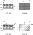
- FIG. 3A is a view 300 similar to FIG. 2A
- FIG. 3B is a view 310 similar to FIG. 2B , after a liner 301 is deposited on the recessed conductive lines 201 according to one embodiment.
- Liner 301 is deposited on the bottom and sidewalls of the trenches 202, as shown in FIG. 3 .
- the liner 301 is an optional component and may not be incorporated in all embodiments of the disclosure.
- the liner 301 is deposited on the recessed first conductive lines 201 and the first insulating layer 102 prior to depositing a second insulating layer (as discussed below). Another embodiment of the method performed without a liner 301 is described below.
- liner 301 is deposited to protect the first conductive lines 201 from changing properties in a later process (e.g., during tungsten deposition, or other processes).
- liner 301 is a conductive liner.
- liner 301 is a non-conductive liner.
- the liner 301 when liner 301 is a non-conductive liner, the liner 301 is removed later on in a process, as described in further detail below.
- the liner helps avoid exposure of the first conductive lines 201 to a low-k dielectric (including ultra low-k dielectrics) and/or serves as an etch stop layer for a self-guided via etch.
- the liner 301 can be any suitable material depending on, for example, the composition of the first conductive lines 201, the first insulating layer 102 and subsequent second insulating layer 401.
- the liner 301 is a dielectric material.
- liner 301 comprises one or more of titanium nitride (TiN), titanium (Ti), tantalum (Ta), tantalum nitride (TaN), silicon carbonitride (SiCN), silicon carbide (SiC), silicon nitride (SiN), aluminum oxide (AIO), aluminum nitride (AIN), hafnium oxide (HfO), titanium oxide (TiO).
- HfO hafnium oxide film
- each of the elements of the formula is present in an amount greater than or equal to about 5%, 10%, 15%, 20%, 25%, 30%, 35%, 40% or 45%, on an atomic basis.
- the liner 301 is deposited to the thickness in the range of about 0.5 nm to about 10 nm.
- the liner 301 is deposited using an atomic layer deposition (ALD) technique.
- ALD atomic layer deposition
- the liner 301 is deposited using one of deposition techniques, such as but no limited to a CVD, PVD, MBE, MOCVD, spin-on, or other liner deposition techniques know to one of ordinary skill in the art of microelectronic device manufacturing.
- the liner 301 is deposited as a conformal film.
- the term "conformal" means that the thickness of the liner 301 at any point on the sidewalls 204 of the trench 202 or top surface 203 of the conductive line 201 does not vary by more than ⁇ 10%, ⁇ 5%, ⁇ 2% or ⁇ 1 % relative to the average thickness of the liner 301.
- FIG. 4A is a view 400 similar to FIG. 3A
- FIG. 4B is a view 410 similar to FIG. 3B , after a second insulating layer 401 is deposited on the liner 301 according to one embodiment.
- the second insulating layer 401 is deposited as a gapfill layer to fill the gaps formed by the recessed first conductive lines 201 in the trenches 202 with the liner 301 on top.
- the second insulating layer 401 is deposited so that an overburden 402 is formed on top of the liner 301 on the top of the first insulating layer 102.
- the overburden can be any suitable thickness and may be removed in a subsequent process. In some embodiments, the overburden is a known amount and is not removed by the process described below in FIGS. 5A-6B .
- the second insulating layer 401 is a low-k dielectric material.
- the second insulating layer 401 comprises a flowable silicon oxycarbide (f-SiOC) film or a low-k gapfill film.
- the second insulating layer 401 is deposited using one of deposition techniques, such as but not limited to an ALD, a CVD, PVD, MBE, MOCVD, spin-on or other liner deposition techniques known to one of ordinary skill in the art of microelectronic device manufacturing.
- FIG. 5A is a view 500 similar to FIG. 4A
- FIG. 5B is a view 510 similar to FIG. 4B , after portions of the second insulating layer 401 are removed to expose top portions 302 of the liner 301 according to one embodiment.
- the planarization process stops at the liner 301 to leave the top surface 403 of the second insulating layer 401 substantially coplanar with the top portions 302 of the liner 301.
- the planarization process does not expose the first insulating layer 102 through the liner 301.
- the second insulating layer 401 can be removed using one of the chemical-mechanical polishing (CMP) techniques known to one of ordinary skill in the art of microelectronic device manufacturing.
- CMP chemical-mechanical polishing
- FIG. 6A is a view 600 similar to FIG. 5A
- FIG. 6B is a view 610 similar to FIG. 5B
- additional second insulating layer 601 is deposited on the planarized second insulating layer 401 and liner 301.
- the additional second insulating layer 601 can be the same composition as the second insulating layer 401 or a different composition.
- the additional second insulating layer 601 is the same material as the second insulating layer 401 so that the combination of the second insulating layer 401 in the gaps of the liner 301 forms a seamless layer with the additional second insulating layer 601 and is referred to as the second insulating layer 601.
- the second insulating layer 601 is formed so that there is a thickness T of the second insulating layer 601 on the top of the liner 301.
- the thickness of the second insulating layer is about the same thickness that will be used in a later trench depth in a dual damascene structure.
- second insulating layer 601 comprises one or more of a flowable silicon oxide (f-SiO) layer.
- second insulating layer 601 comprises an oxide layer, e.g., silicon dioxide, or any other electrically insulating layer determined by an electronic device design.
- second insulating layer 601 is an interlayer dielectric (ILD).
- second insulating layer 601 is a low-k dielectric that includes, but is not limited to, materials such as, e.g., silicon dioxide, silicon oxide, a carbon based material, e.g, a porous carbon film, carbon doped oxide ("CDO"), e.g., carbon doped silicon dioxide, porous silicon dioxide, porous silicon oxide carbide hydride (SiOCH), silicon nitride, or any combination thereof.
- second insulating layer 601 is a dielectric material having k-value less than 3.
- second insulating layer 601 is a dielectric material having k-value in an approximate range from about 2.2 to about 2.7.
- second insulating layer 601 includes a dielectric material having k-value less than 2.
- second insulating layer 601 represents one of the insulating layers described above with respect to insulating layer 102.
- second insulating layer 601 is a low-k interlayer dielectric to isolate one conductive line 201 from adjacent conductive lines 201.
- second insulating layer 601 is deposited using one of deposition techniques, such as but not limited to a CVD, spin-on, an ALD, PVD. MBE, MOCVD, or other low-k insulating layer deposition techniques known to one of ordinary skill in the art of microelectronic device manufacturing.
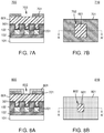
- FIG. 7A is a view 700 similar to FIG. 6A
- FIG. 7B is a view 710 similar to FIG. 6B after a hardmask 701 is formed on second insulating layer 601 according to one embodiment.
- hardmask 701 is a metallization layer hardmask.
- the hardmask 701 has a first opening 702 that is aligned in the Z axis over one of the first conductive lines 201.
- the hardmask 701 material is deposited on the second insulating layer 601 and the hardmask 701 is patterned using trench lithography to form one or more first opening 702.
- the dimensions and shape of the first openings 702 in the hardmask 701 can vary depending on the configuration of the electronic device structure being formed. In some embodiments, the first openings 702 are wider than the first conductive line 201 aligned with the first opening 702.
- the hardmask 701 can be any suitable material including, but not limited to, titanium nitride, tungsten carbide or tungsten borocarbide.
- hardmask 701 is a carbon hardmask layer, a metal oxide hardmask layer, a metal nitride hardmask layer, a silicon nitride hardmask layer, a silicon oxide hardmask layer, a carbide hardmask layer, or other hardmask layer known to one of ordinary skill in the art of microelectronic device manufacturing.
- the hardmask 701 is formed using one or more hard mask patterning techniques known to one of ordinary skill in the art of microelectronic device manufacturing.
- FIG. 8A is a view 800 similar to FIG. 7A
- FIG. 8B is a view 810 similar to FIG. 7B , after a photoresist 801 is formed on hardmask 701.
- the photoresist 801 includes a second opening 802 aligned with the first opening 702 so that the second opening 802 is formed above one of the first conductive lines 201.
- forming the photoresist 801 on the hardmask 701 comprises a selective deposition process where the photoresist 801 material is deposited substantially only on the hardmask 701 and not on the second insulating layer 601 exposed through the first opening 702.
- the photoresist 801 is formed as a conformal layer of the photoresist material on the hardmask 701 and the second insulating layer 601 is exposed through the first opening 702 and second opening 802 through lithographic patterning.
- the size of the second opening 802 can be the same as the size of the first opening 702 or different.
- the photoresist 801 is selectively deposited on the hardmask 701 so that the sides of the first opening 702 are covered and creating a smaller second opening 802.
- the size and dimensions of the second opening 802 are greater than the width of the first conductive line 201 with which the second opening 802 is aligned.
- the photoresist 801 includes a bottom anti-reflective coating (BARC) layer.
- photoresist 801 is deposited using one of deposition techniques, such as but not limited to, a CVD, PVD, MBE, PECVD, spin-on, or other insulating layer deposition techniques known to one of ordinary skill in the art of microelectronic device manufacturing.
- the second opening 802 is formed using one or more of the patterning and etching techniques known to one of ordinary skill in the art of microelectronic device manufacturing.
- FIG. 9A is a view 900 similar to FIG. 8A
- FIG. 9B is a view 910 similar to FIG. 8B , after the second insulating layer 601 is partially etched through the second opening 802 to form opening 901.
- the second insulating layer 601 is selectively etched through second opening 802 to form an opening 901 according to one embodiment.
- the etch process used to remove portions of the second insulating layer 601 is selective to the second insulating layer 601 relative to one or more of the liner 301 or the first insulating layer 102.
- FIG. 10A is a view 1000 similar to FIG. 9A
- FIG. 10B is a view 1010 similar to FIG. 9B , after removal of the photoresist 801 to leave hardmask 701 with first opening 702 on the second insulating layer 601.
- the second opening 802 was smaller than the first opening 702
- removing the photoresist 801 exposes a top surface 1001 of the second insulating layer 601.
- a top surface 1001 of the second insulating layer 601 is not exposed.
- removing the photoresist 801 comprises a process that is selective to the photoresist 801 relative to the hardmask 701 and the second insulating layer 601.
- photoresist 801 is removed using one or more of the removal techniques known to one of ordinary skill in the art of microelectronic device manufacturing.
- FIG. 11A is a view 1100 similar to FIG. 10A
- FIG. 11B is a view 1110 similar to FIG. 10B , after etching the second insulating layer 601 through the first opening 702 to form trench 1101.
- the etch process of some embodiments is selective to the second insulating material 601 relative to the liner 301 or the first insulating layer 102, so that the etch process stops at the liner 301.
- an isotropic etch process through first opening 702 exposes the liner 301 on top 1102 of the first conductive line 201 aligned with the first opening 702 and the liner 301 on top 1103 of the first insulating layer 102 adjacent the first conductive line 201.
- etching the second insulating layer 601 is a self-guided process and is confined to a recess trench 1101 aligned with one of the first conductive lines 201. In some embodiments, etching the second insulating layer 601 is accomplished using one or more of the removal techniques known to one of ordinary skill in the art of microelectronic device manufacturing.
- FIG. 12A is a view 1200 similar to FIG. 11A
- FIG. 12B is a view 1210 similar to FIG. 11B , after removal of the liner 301 exposed through trench 1101 to form via 1201.
- the liner 301 is removed after etching through the second insulating layer 601 through the first opening 702 to expose the top surface 203 of the first conductive line 201 aligned with the first opening 702 and the sidewall 1203 of the via 1201.
- removal of the liner 301 comprises a selective etch process that is selective to the liner 301 relative to the second insulating layer 601, first insulating layer 102 and first conductive line 201.
- the liner 301 is removed by one or more of a dry removal process or a wet removal process. Removing the liner 301 increases the critical dimension (i.e., width of the via above the exposed first conductive line 201) for further processing. In some embodiments, the liner 301 is removed using one or more of the removal techniques known to one of ordinary skill in the art of microelectronic device manufacturing.
- FIG. 13A is a view 1300 similar to FIG. 12A
- FIG. 13B is a view 1310 similar to FIG. 12B , after removal of the hardmask 701 from the second insulating layer 601.
- Removal of the hardmask 701 leaves via 1201 with the top surface 203 of the first conductive line 201 and top surface 1202 of the adjacent first insulating layer 102.
- Removal of the hardmask 701 can be done using a process that is selective to the hardmask 701 relative to the first conductive line 201, first insulating layer 102 and second insulating layer 601.
- removal of the hardmask 701 occurs at the same time as removal of the liner 301 so that the process is selective for the hardmask 701 and liner 301 relative to the first insulating layer 102, second insulating layer 601 and first conductive line 201.
- hardmask 701 is removed using one or more of the mask layer removal techniques known to one of ordinary skill in the art of microelectronic device manufacturing.
- FIG. 14A is a view 1400 similar to FIG. 13A
- FIG. 14B is a view 1410 similar to FIG. 13B , after a second conductive line 1401 is deposited into via 1201.
- forming the second conductive line 1401 involves filling the via 1201 with a layer of conductive material.
- a base layer (not shown) is first deposited on the internal sidewalls and bottom of the via 1201 and then the conductive layer is deposited on the base layer.
- the base layer includes a conductive seed layer (not shown) deposited on a conductive barrier layer (not shown).
- the seed layer can include copper, and the conductive barrier layer can include aluminum, titanium, tantalum, tantalum nitride, and the like metals.
- the conductive barrier layer can be used to prevent diffusion of the conductive material from the seed layer, e.g., copper, into the insulating layer. Additionally, the conductive barrier layer can be used to provide adhesion for the seed layer (e.g, copper).
- the conductive barrier layer is deposited onto the sidewalls and bottom of the trenches, and then the seed layer is deposited on the conductive barrier layer.
- the conductive base layer includes the seed layer that is directly deposited onto the sidewalls and bottom of the trenches.
- Each of the conductive barrier layer and seed layer may be deposited using any thin film deposition technique known to one of ordinary skill in the art of semiconductor manufacturing, e.g., sputtering, blanket deposition, and the like.
- each of the conductive barrier layer and the seed layer has the thickness in an approximate range from about 1 nm to about 100 nm.
- the barrier layer may be a thin dielectric that has been etched to establish conductivity to the metal layer below. In some embodiments, the barrier layer may be omitted altogether and appropriate doping of the copper line may be used to make a "self-forming barrier".
- the conductive layer e.g., copper
- the conductive layer is deposited onto the seed layer of base later of copper, by an electroplating process.
- the conductive layer is deposited into the trenches using a damascene process known to one of ordinary skill in the art of microelectronic device manufacturing.
- the conductive layer is deposited onto the seed layer in the trenches and in the opening using a selective deposition technique, such as but not limited to electroplating, electroless, a CVD, PVD, MBE, MOCVD, ALD, spin-on, or other deposition techniques known to one of ordinary skill in the art of microelectronic device manufacturing.
- the choice of a material for second conductive lines 1401 determines the choice of a material for the seed layer.
- the material for the seed layer may also include copper.
- the second conductive line 1401 include a metal, for example, copper (Cu), ruthenium (Ru), nickel (Ni), cobalt (Co), chromium (Cr), iron (Fe), manganese (Mn), titanium (Ti), aluminum (Al), hafnium (Hf), tantalum (Ta), tungsten (W), vanadium (V), molybdenum (Mo), palladium (Pd), gold (Au), silver (Ag), platinum (Pt), indium (In), tin (Sn), lead (Pb), antimony (Sb), bismuth (Bi), zinc (Zn), cadmium (Cd), or any combination thereof.
- examples of the conductive materials that may be used for the conductive lines 1401 include, but not limited to, metal alloys, metal carbides, e.g., hafnium carbide, zirconium carbide, titanium carbide, tantalum carbide, aluminum carbide, other conductive materials, or any combination thereof.
- metal alloys metal carbides, e.g., hafnium carbide, zirconium carbide, titanium carbide, tantalum carbide, aluminum carbide, other conductive materials, or any combination thereof.
- depositing the second conductive line 1401 comprises depositing a second conductive material in the via 1201 and on the top surface 602 of the second insulating layer 601, forming an overburden.
- the portions of the conductive material on the top surface 602 i.e., the overburden
- CMP chemical-mechanical polishing
- the thickness (measured along the Z axis direction) of the second conductive lines 1401 is in an approximate range from about 15 nm to about 1000 nm. In some embodiments, the thickness of the conductive lines 1401 is from about 20 nm to about 200 nm. In some embodiments, the width (measured along the Y axis direction) of the conductive lines 1401 is in an approximate range from about 5 nm to about 500 nm. In some embodiments, the spacing (pitch) between the conductive lines 1401 (measured along the Y axis direction) is from about 2 nm to about 500 nm, or in the range of about 5 nm to about 50 nm.
- FIGS. 15A through 24B Another embodiment of the disclosure is described with respect to FIGS. 15A through 24B .
- the process does not includes liner 301.
- Similar components of FIGS. 15A through 24B to those of FIGS. 1A through 14B use the same reference numerals.
- FIG. 15A is a view 1500 similar to FIG. 2A
- FIG. 15B is a view 1510 similar to FIG. 2B
- a second insulating layer 401 is deposited on the first insulating layer 102 and the first conductive lines 201 according to one embodiment.
- the second insulating layer 401 is deposited as a gapfill layer to fill the gaps formed by the recessed first conductive lines 201 in the trenches 202.
- the second insulating layer 401 is deposited so that an overburden 402 is formed on top of the first insulating layer 102.
- the overburden can be any suitable thickness and may be removed in a subsequent process. In some embodiments, the overburden is a known amount and is not removed by the process described below in FIGS. 16A-17B .
- the second insulating layer 401 is a low-k dielectric material.
- the second insulating layer 401 comprises a flowable silicon oxycarbide (f-SiOC) film or a low-k gapfill film.
- the second insulating layer 401 is deposited using one of deposition techniques, such as but not limited to an ALD, a CVD, PVD, MBE, MOCVD, spin-on or other liner deposition techniques known to one of ordinary skill in the art of microelectronic device manufacturing.
- FIG. 16A is a view 1600 similar to FIG. 15A
- FIG. 16B is a view 1610 similar to FIG. 15B
- the planarization process stops to leave the top surface 403 of the second insulating layer 401 substantially coplanar with the top surface 105 of the first insulating layer 102.
- the overburden 402 of the second insulating layer 401 can be removed using one of the chemical-mechanical polishing (CMP) techniques known to one of ordinary skill in the art of microelectronic device manufacturing.
- CMP chemical-mechanical polishing
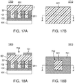
- FIG. 17A is a view 1700 similar to FIG. 16A
- FIG. 17B is a view 1710 similar to FIG. 16B
- additional second insulating layer 601 is deposited on the planarized top surface 105 of the first insulating layer 102 and the top surface 403 of the second insulating layer 401.
- the additional second insulating layer 601 can be the same composition as the second insulating layer 401 or a different composition.
- the additional second insulating layer 601 is the same material as the second insulating layer 401 so that the combination forms a seamless layer and is referred to as the second insulating layer 601.
- the second insulating layer 601 is formed so that there is a thickness T of the second insulating layer 601 on the top of the liner 301.
- the thickness of the second insulating layer is about the same thickness that will be used in a later trench depth in a dual damascene structure.
- second insulating layer 601 comprises one or more of a flowable silicon oxide (f-SiO) layer.
- second insulating layer 601 comprises an oxide layer, e.g., silicon dioxide, or any other electrically insulating layer determined by an electronic device design.
- second insulating layer 601 is an interlayer dielectric (ILD).
- second insulating layer 601 is a low-k dielectric that includes, but is not limited to, materials such as, e.g., silicon dioxide, silicon oxide, a carbon based material, e.g, a porous carbon film, carbon doped oxide ("CDO"), e.g., carbon doped silicon dioxide, porous silicon dioxide, porous silicon oxide carbide hydride (SiOCH), silicon nitride, or any combination thereof.
- second insulating layer 601 is a dielectric material having k-value less than 3.
- second insulating layer 601 is a dielectric material having k-value in an approximate range from about 2.2 to about 2.7.
- second insulating layer 601 includes a dielectric material having k-value less than 2.
- second insulating layer 601 represents one of the insulating layers described above with respect to insulating layer 102.
- second insulating layer 601 is a low-k interlayer dielectric to isolate one conductive line 201 from adjacent conductive lines 201.
- second insulating layer 601 is deposited using one of deposition techniques, such as but not limited to a CVD, spin-on, an ALD, PVD. MBE, MOCVD, or other low-k insulating layer deposition techniques known to one of ordinary skill in the art of microelectronic device manufacturing.
- FIG. 18A is a view 1800 similar to FIG. 17A
- FIG. 18B is a view 1810 similar to FIG. 17B after a hardmask 701 is formed on second insulating layer 601 according to one embodiment.
- hardmask 701 is a metallization layer hardmask.
- the hardmask 701 has a first opening 702 that is aligned in the Z axis over one of the first conductive lines 201.
- the hardmask 701 is deposited on the second insulating layer 601 and the hardmask 701 is patterned using trench lithography to form one or more first opening 702.
- the dimensions and shape of the first openings 702 in the hardmask 701 can vary depending on the configuration of the electronic device structure being formed. In some embodiments, the first openings 702 are wider than the first conductive line 201 aligned with the first opening 702.
- the hardmask 701 can be any suitable material including, but not limited to, titanium nitride, tungsten carbide or tungsten borocarbide.
- hardmask 701 is a carbon hardmask layer, a metal oxide hardmask layer, a metal nitride hardmask layer, a silicon nitride hardmask layer, a silicon oxide hardmask layer, a carbide hardmask layer, or other hardmask layer known to one of ordinary skill in the art of microelectronic device manufacturing.
- the hardmask 701 is formed using one or more hard mask patterning techniques known to one of ordinary skill in the art of microelectronic device manufacturing.
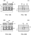
- FIG. 19A is a view 1900 similar to FIG. 18A
- FIG. 19B is a view 1910 similar to FIG. 18B , after a photoresist 801 is formed on hardmask 701.
- the photoresist 801 includes a second opening 802 aligned with the first opening 702 so that the second opening 802 is formed above one of the first conductive lines 201.
- forming the photoresist 801 on the hardmask 701 comprises a selective deposition process where the photoresist 801 material is deposited substantially only on the hardmask 701 and not on the second insulating layer 601 exposed through the first opening 702.
- the photoresist 801 is formed as a conformal layer of the photoresist material on the hardmask 701 and the second insulating layer 601 is exposed through the first opening 702 and second opening 802 through lithographic patterning.
- the size of the second opening 802 can be the same as the size of the first opening 702 or different.
- the photoresist 801 is selectively deposited on the hardmask 701 so that the sides of the first opening 702 are covered and creating a smaller second opening 802.
- the size and dimensions of the second opening 802 are greater than the width of the first conductive line 201 with which the second opening 802 is aligned.
- the photoresist 801 includes a bottom anti-reflective coating (BARC) layer.
- photoresist 801 is deposited using one of deposition techniques, such as but not limited to, a CVD, PVD, MBE, PECVD, spin-on, or other insulating layer deposition techniques known to one of ordinary skill in the art of microelectronic device manufacturing.
- the second opening 802 is formed using one or more of the patterning and etching techniques known to one of ordinary skill in the art of microelectronic device manufacturing.
- FIG. 20A is a view 2000 similar to FIG. 19A
- FIG. 20B is a view 2010 similar to FIG. 19B , after the second insulating layer 601 is partially etched through the second opening 802 to form opening 901.
- the second insulating layer 601 is selectively etched through second opening 802 to form an opening 901 according to one embodiment.
- the etch process used to remove portions of the second insulating layer 601 is selective to the second insulating layer 601 relative to the first insulating layer 102.
- FIG. 21A is a view 2100 similar to FIG. 20A
- FIG. 21B is a view 2110 similar to FIG. 20B , after removal of the photoresist 801 to leave hardmask 701 with first opening 702 on the second insulating layer 601.
- the second opening 802 was smaller than the first opening 702
- removing the photoresist 801 exposes a top surface 1001 of the second insulating layer 601.
- a top surface 1001 of the second insulating layer 601 is not exposed.
- removing the photoresist 801 comprises a process that is selective to the photoresist 801 relative to the hardmask 701 and the second insulating layer 601.
- photoresist 801 is removed using one or more of the removal techniques known to one of ordinary skill in the art of microelectronic device manufacturing.
- FIG. 22A is a view 2200 similar to FIG. 21A
- FIG. 22B is a view 2210 similar to FIG. 21B , after etching the second insulating layer 601 through the first opening 702 to form trench 1101.
- the etch process of some embodiments is selective to the second insulating layer 601 relative to the first insulating layer 102 and/or the first conductive lines 201, so that the etch process stops at the first conductive lines 201.
- an isotropic etch process through first opening 702 exposes the top surface 203 of the first conductive line 201 aligned with the first opening 702 and the top surface 1202 of the first insulating layer 102 adjacent the first conductive line 201.
- the etch process for the second insulating layer 601 has a selectivity relative to the first insulating layer 102 of greater than or equal to about 5:1. As illustrated in FIG. 22A , rounded corners 2202 of the top surface 1202 of the first insulating layer 102 can be formed during the etch process because some amount of the first insulating layer 102 may be removed. This may open the critical dimension of the via to allow for easier gapfilling with the second conductive lines in a subsequent process.
- etching the second insulating layer 601 is a self-guided process and is confined to a recess trench aligned with one of the first conductive lines 201. In some embodiments, etching the second insulating layer 601 is accomplished using one or more of the removal techniques known to one of ordinary skill in the art of microelectronic device manufacturing.
- FIG. 23A is a view 2300 similar to FIG. 22A
- FIG. 23B is a view 2310 similar to FIG. 22B , after removal of the hardmask 701 from the second insulating layer 601.
- Removal of the hardmask 701 leaves via 1201 with the top surface 203 of the first conductive line 201 and top surface 1202 of the adjacent first insulating layer 102.
- Removal of the hardmask 701 can be done using a process that is selective to the hardmask 701 relative to the first conductive line 201, first insulating layer 102 and second insulating layer 601.
- hardmask 701 is removed using one or more of the mask layer removal techniques known to one of ordinary skill in the art of microelectronic device manufacturing.
- FIG. 24A is a view 2400 similar to FIG. 23A
- FIG. 24B is a view 2410 similar to FIG. 23B , after a second conductive line 1401 is deposited into via 1201.
- forming the second conductive line 1401 involves filling the via 1201 with a layer of conductive material.
- a base layer (not shown) is first deposited on the internal sidewalls and bottom of the via 1201 and then the conductive layer is deposited on the base layer.
- the base layer includes a conductive seed layer (not shown) deposited on a conductive barrier layer (not shown).
- the seed layer can include copper, and the conductive barrier layer can include aluminum, titanium, tantalum, tantalum nitride, and the like metals.
- the conductive barrier layer can be used to prevent diffusion of the conductive material from the seed layer, e.g., copper, into the insulating layer. Additionally, the conductive barrier layer can be used to provide adhesion for the seed layer (e.g, copper).
- the conductive barrier layer is deposited onto the sidewalls and bottom of the trenches, and then the seed layer is deposited on the conductive barrier layer.
- the conductive base layer includes the seed layer that is directly deposited onto the sidewalls and bottom of the trenches.
- Each of the conductive barrier layer and seed layer may be deposited using any thin film deposition technique known to one of ordinary skill in the art of semiconductor manufacturing, e.g., sputtering, blanket deposition, and the like.
- each of the conductive barrier layer and the seed layer has the thickness in an approximate range from about 1 nm to about 100 nm.
- the barrier layer may be a thin dielectric that has been etched to establish conductivity to the metal layer below. In some embodiments, the barrier layer may be omitted altogether and appropriate doping of the copper line may be used to make a "self-forming barrier".
- the conductive layer e.g., copper
- the conductive layer is deposited onto the seed layer of base later of copper, by an electroplating process.
- the conductive layer is deposited into the trenches using a damascene process known to one of ordinary skill in the art of microelectronic device manufacturing.
- the conductive layer is deposited onto the seed layer in the trenches and in the opening using a selective deposition technique, such as but not limited to electroplating, electroless, a CVD, PVD, MBE, MOCVD, ALD, spin-on, or other deposition techniques known to one of ordinary skill in the art of microelectronic device manufacturing.
- the choice of a material for second conductive lines 1401 determines the choice of a material for the seed layer.
- the material for the seed layer may also include copper.
- the second conductive line 1401 include a metal, for example, copper (Cu), ruthenium (Ru), nickel (Ni), cobalt (Co), chromium (Cr), iron (Fe), manganese (Mn), titanium (Ti), aluminum (Al), hafnium (Hf), tantalum (Ta), tungsten (W), vanadium (V), molybdenum (Mo), palladium (Pd), gold (Au), silver (Ag), platinum (Pt), indium (In), tin (Sn), lead (Pb), antimony (Sb), bismuth (Bi), zinc (Zn), cadmium (Cd), or any combination thereof.
- examples of the conductive materials that may be used for the conductive lines 1401 include, but not limited to, metal alloys, metal carbides, e.g., hafnium carbide, zirconium carbide, titanium carbide, tantalum carbide, aluminum carbide, other conductive materials, or any combination thereof.
- metal alloys metal carbides, e.g., hafnium carbide, zirconium carbide, titanium carbide, tantalum carbide, aluminum carbide, other conductive materials, or any combination thereof.
- depositing the second conductive line 1401 comprises depositing a second conductive material in the via 1201 and on the top surface 602 of the second insulating layer 601, forming an overburden.
- the portions of the conductive material on the top surface 602 i.e., the overburden
- CMP chemical-mechanical polishing
- the thickness (measured along the Z axis direction) of the second conductive lines 1401 is in an approximate range from about 15 nm to about 1000 nm. In some embodiments, the thickness of the conductive lines 1401 is from about 20 nm to about 200 nm. In some embodiments, the width (measured along the Y axis direction) of the conductive lines 1401 is in an approximate range from about 5 nm to about 500 nm. In some embodiments, the spacing (pitch) between the conductive lines 1401 (measured along the Y axis direction) is from about 2 nm to about 500 nm, or in the range of about 5 nm to about 50 nm.
- FIG. 25 shows a block diagram of a plasma system to perform at least some of the operations to provide a fully self-aligned via according to one embodiment.
- system 2500 has a processing chamber 2501.
- a movable pedestal 2502 to hold an electronic device structure 2503 is placed in processing chamber 2501.
- Pedestal 2502 comprises an electrostatic chuck ("ESC"), a DC electrode embedded into the ESC, and a cooling/heating base.
- ESC electrostatic chuck
- pedestal 2502 acts as moving cathode.
- the ESC comprises an Al 2 O 3 material, Y 2 O 3 or other ceramic materials known to one of ordinary skill of electronic device manufacturing.
- a DC power supply 2504 is connected to the DC electrode of the pedestal 2502.
- System 2500 comprises an inlet to input one or more process gases 2512 through a mass flow controller 2511 to a plasma source 2513.
- a plasma source 2513 comprising a showerhead 2514 is coupled to the processing chamber 2501 to receive one or more gases 2512 to generate plasma.
- Plasma source 2513 is coupled to a RF source power 2510.
- Plasma source 2513 through showerhead 2514 generates a plasma 2515 in processing chamber 2501 from one or more process gases 2512 using a high frequency electric field.
- Plasma 2515 comprises plasma particles, such as ions, electrons, radicals, or any combination thereof.
- power source 2510 supplies power from about 50W to about 3000W at a frequency from about 400kHz to about 162MHz to generate plasma 2515.
- a plasma bias power 2505 is coupled to the pedestal 2502 (e.g., cathode) via a RF match 2507 to energize the plasma.
- the plasma bias power 2505 provides a bias power that is not greater than 1000W at a frequency between about 2MHz to 60 MHz, and in a particular embodiment at about 13MHz.
- a plasma bias power 2506 may also be provided, for example, to provide another bias power that is not greater than 1000W at a frequency from about 400kHz to about 60 MHz, and in a particular embodiment, at about 60 MHz.
- Plasma bias power 2506 and bias power 2505 are connected to RF match 2507 to provide a dual frequency bias power.
- a total bias power applied to the pedestal 2502 is from about 10 W to about 3000 W.
- a pressure control system 2509 provides a pressure to processing chamber 2501.
- chamber 2501 has one or more exhaust outlets 2516 to evacuate volatile products produced during processing in the chamber.
- the plasma system 2500 is an inductively coupled plasma (ICP) system.
- the plasma system 2500 is a capacitively coupled plasma (CCP) system.
- a control system 2517 is coupled to the chamber 2501.
- the control system 2517 comprises a processor 2518, a temperature controller 2519 coupled to the processor 2518, a memory 2520 coupled to the processor 2518, and input/output devices 2521 coupled to the processor 2518 to form fully self-aligned via as described herein.
- the processor 2518 has a configuration to control recessing first conductive lines on a first insulating layer on a substrate, the first conductive lines extending along a first direction on the first insulating layer. In some embodiments, the processor 2518 has a configuration to control depositing a liner on the recessed first conductive lines. In some embodiments, the processor 2518 has a configuration to control depositing a second insulating layer. In some embodiments, the processor 2518 has a configuration to control removal of an overburden of the second insulating layer. In some embodiments, the process 2518 has a configuration to deposit a predetermined amount of the second insulating layer. In some embodiments, the processor 2518 has a configuration to form a hardmask.
- the processor 2518 has a configuration to control forming a first opening in the hardmask. In some embodiments, the processor 2518 has a configuration to control forming a photoresist. In some embodiments, the processor 2518 has a configuration to control forming a second opening in the photoresist. In some embodiments, the processor 2518 has a configuration to control etching the second insulating layer through the second opening. In some embodiments, the processor 2518 has a configuration to control removing the photoresist. In some embodiments, the processor 2518 has a configuration to control etching the second insulating layer to form a fully self-aligned via opening down to one of the first conductive lines or a liner on the first conductive line. In some embodiments, the processor 2518 has a configuration to selectively remove the liner exposed through the via. In some embodiments, the processor 2518 has a configuration to control depositing a conductive layer into the self-aligned via opening, as described above.
- the control system 2517 is configured to perform at least some of the methods as described herein and may be either software or hardware or a combination of both.
- the plasma system 2500 may be any type of high performance processing plasma systems known in the art, such as but not limited to, an etcher, a cleaner, a furnace, or any other plasma system to manufacture electronic devices.
Landscapes
- Internal Circuitry In Semiconductor Integrated Circuit Devices (AREA)
- Chemical & Material Sciences (AREA)
- Inorganic Chemistry (AREA)
- Drying Of Semiconductors (AREA)
Applications Claiming Priority (1)
| Application Number | Priority Date | Filing Date | Title |
|---|---|---|---|
| US201762599664P | 2017-12-15 | 2017-12-15 |
Publications (1)
| Publication Number | Publication Date |
|---|---|
| EP3499557A1 true EP3499557A1 (fr) | 2019-06-19 |
Family
ID=64664064
Family Applications (1)
| Application Number | Title | Priority Date | Filing Date |
|---|---|---|---|
| EP18211015.5A Withdrawn EP3499557A1 (fr) | 2017-12-15 | 2018-12-07 | Procédés pour vias auto-alignés gravés sélectivement |
Country Status (6)
| Country | Link |
|---|---|
| US (1) | US10593594B2 (fr) |
| EP (1) | EP3499557A1 (fr) |
| JP (1) | JP6793711B2 (fr) |
| KR (1) | KR102219125B1 (fr) |
| CN (1) | CN110021555B (fr) |
| TW (1) | TW201928510A (fr) |
Families Citing this family (12)
| Publication number | Priority date | Publication date | Assignee | Title |
|---|---|---|---|---|
| WO2019050735A1 (fr) * | 2017-09-06 | 2019-03-14 | Micromaterials Llc | Procédés de production de trous d'interconnexion auto-alignés |
| EP3499557A1 (fr) | 2017-12-15 | 2019-06-19 | Micromaterials LLC | Procédés pour vias auto-alignés gravés sélectivement |
| US11380581B2 (en) * | 2018-11-09 | 2022-07-05 | Globalfoundries U.S. Inc. | Interconnect structures of semiconductor devices having a via structure through an upper conductive line |
| US11715643B2 (en) * | 2019-07-18 | 2023-08-01 | Tokyo Electron Limited | Gas phase etch with controllable etch selectivity of metals |
| US11094588B2 (en) * | 2019-09-05 | 2021-08-17 | Applied Materials, Inc. | Interconnection structure of selective deposition process |
| US11069610B2 (en) | 2019-10-15 | 2021-07-20 | Micron Technology, Inc. | Methods for forming microelectronic devices with self-aligned interconnects, and related devices and systems |
| TWI828985B (zh) * | 2020-06-10 | 2024-01-11 | 美商應用材料股份有限公司 | 完全自對準減法蝕刻 |
| US11469140B2 (en) * | 2020-08-25 | 2022-10-11 | Nanya Technology Corporation | Semiconductor device having a landing pad with spacers and method for fabricating the same |
| US11482454B2 (en) | 2021-02-17 | 2022-10-25 | Tokyo Electron Limited | Methods for forming self-aligned contacts using spin-on silicon carbide |
| JP2024523510A (ja) * | 2021-07-06 | 2024-06-28 | 東京エレクトロン株式会社 | 自己組織化単分子層を使用する選択的な膜形成 |
| WO2023027827A1 (fr) * | 2021-08-24 | 2023-03-02 | Applied Materials, Inc. | Procédés d'intégration de trou d'interconnexion entièrement auto-aligné |
| US12266564B2 (en) * | 2022-01-26 | 2025-04-01 | Nanya Technology Corporation | Semiconductor device |
Citations (4)
| Publication number | Priority date | Publication date | Assignee | Title |
|---|---|---|---|---|
| US20020090812A1 (en) * | 2001-01-09 | 2002-07-11 | Macronix International Co., Ltd. | Method for forming trench |
| US20170053863A1 (en) * | 2015-08-19 | 2017-02-23 | Taiwan Semiconductor Manufacturing Company, Ltd. | Structure and Method for Interconnection |
| US9685406B1 (en) * | 2016-04-18 | 2017-06-20 | International Business Machines Corporation | Selective and non-selective barrier layer wet removal |
| US20170271202A1 (en) * | 2016-03-21 | 2017-09-21 | Qualcomm Incorporated | FORMING SELF-ALIGNED VERTICAL INTERCONNECT ACCESSES (VIAs) IN INTERCONNECT STRUCTURES FOR INTEGRATED CIRCUITS (ICs) |
Family Cites Families (102)
| Publication number | Priority date | Publication date | Assignee | Title |
|---|---|---|---|---|
| US4671970A (en) | 1986-02-05 | 1987-06-09 | Ncr Corporation | Trench filling and planarization process |
| KR0165813B1 (ko) | 1995-04-12 | 1999-02-01 | 문정환 | 접속홀의 플러그 형성 방법 |
| US5872052A (en) | 1996-02-12 | 1999-02-16 | Micron Technology, Inc. | Planarization using plasma oxidized amorphous silicon |
| KR100223334B1 (ko) | 1996-06-29 | 1999-10-15 | 김영환 | 반도체소자의 금속배선형성방법 |
| US6143653A (en) | 1998-10-04 | 2000-11-07 | Promos Technologies, Inc. | Method of forming tungsten interconnect with tungsten oxidation to prevent tungsten loss |
| KR20000026588A (ko) | 1998-10-21 | 2000-05-15 | 윤종용 | 콘택홀을 갖는 반도체 장치 및 그 제조방법 |
| US6130151A (en) | 1999-05-07 | 2000-10-10 | Taiwan Semiconductor Manufacturing Company | Method of manufacturing air gap in multilevel interconnection |
| JP2001015479A (ja) | 1999-06-29 | 2001-01-19 | Toshiba Corp | 半導体装置の製造方法 |
| WO2001013426A1 (fr) | 1999-08-18 | 2001-02-22 | Steag Rtp Systems, Inc. | Procede de production de structures de cuivre sur des plaquettes de semi-conducteurs |
| US6576113B1 (en) | 1999-10-29 | 2003-06-10 | California Institute Of Technology | Method of electroplating of high aspect ratio metal structures into semiconductors |
| US6373087B1 (en) | 2000-08-31 | 2002-04-16 | Agere Systems Guardian Corp. | Methods of fabricating a metal-oxide-metal capacitor and associated apparatuses |
| US7192803B1 (en) | 2000-10-13 | 2007-03-20 | Bridge Semiconductor Corporation | Method of making a semiconductor chip assembly with simultaneously formed interconnect and connection joint |
| US6653200B2 (en) | 2001-01-26 | 2003-11-25 | Applied Materials, Inc. | Trench fill process for reducing stress in shallow trench isolation |
| JP2002252281A (ja) | 2001-02-27 | 2002-09-06 | Sony Corp | 半導体装置およびその製造方法 |
| US6528884B1 (en) | 2001-06-01 | 2003-03-04 | Advanced Micro Devices, Inc. | Conformal atomic liner layer in an integrated circuit interconnect |
| US7279119B2 (en) | 2001-06-14 | 2007-10-09 | Ppg Industries Ohio, Inc. | Silica and silica-based slurry |
| CN100360710C (zh) | 2002-03-28 | 2008-01-09 | 哈佛学院院长等 | 二氧化硅纳米层压材料的气相沉积 |
| US8298933B2 (en) | 2003-04-11 | 2012-10-30 | Novellus Systems, Inc. | Conformal films on semiconductor substrates |
| US7276787B2 (en) | 2003-12-05 | 2007-10-02 | International Business Machines Corporation | Silicon chip carrier with conductive through-vias and method for fabricating same |
| US7211844B2 (en) | 2004-01-29 | 2007-05-01 | International Business Machines Corporation | Vertical field effect transistors incorporating semiconducting nanotubes grown in a spacer-defined passage |
| KR100923192B1 (ko) | 2004-03-16 | 2009-10-22 | 가부시키가이샤 아이에이치아이 | 반도체 장치의 제조 방법 |
| US7521378B2 (en) | 2004-07-01 | 2009-04-21 | Micron Technology, Inc. | Low temperature process for polysilazane oxidation/densification |
| US7820020B2 (en) | 2005-02-03 | 2010-10-26 | Applied Materials, Inc. | Apparatus for plasma-enhanced physical vapor deposition of copper with RF source power applied through the workpiece with a lighter-than-copper carrier gas |
| US8324660B2 (en) | 2005-05-17 | 2012-12-04 | Taiwan Semiconductor Manufacturing Company, Ltd. | Lattice-mismatched semiconductor structures with reduced dislocation defect densities and related methods for device fabrication |
| JP2007005381A (ja) | 2005-06-21 | 2007-01-11 | Matsushita Electric Ind Co Ltd | プラズマエッチング方法、及びプラズマエッチング装置 |
| US7393789B2 (en) | 2005-09-01 | 2008-07-01 | Micron Technology, Inc. | Protective coating for planarization |
| US7351648B2 (en) | 2006-01-19 | 2008-04-01 | International Business Machines Corporation | Methods for forming uniform lithographic features |
| US7368394B2 (en) | 2006-02-27 | 2008-05-06 | Applied Materials, Inc. | Etch methods to form anisotropic features for high aspect ratio applications |
| US7288463B1 (en) | 2006-04-28 | 2007-10-30 | Novellus Systems, Inc. | Pulsed deposition layer gap fill with expansion material |
| US7956465B2 (en) | 2006-05-08 | 2011-06-07 | Taiwan Semiconductor Manufacturing Company, Ltd. | Reducing resistivity in interconnect structures of integrated circuits |
| JP2008108757A (ja) | 2006-10-23 | 2008-05-08 | Matsushita Electric Works Ltd | 化合物半導体発光素子およびそれを用いる照明装置ならびに化合物半導体素子の製造方法 |
| US7598170B2 (en) | 2007-01-26 | 2009-10-06 | Asm America, Inc. | Plasma-enhanced ALD of tantalum nitride films |
| US20080242097A1 (en) | 2007-03-28 | 2008-10-02 | Tim Boescke | Selective deposition method |
| US20090017631A1 (en) | 2007-06-01 | 2009-01-15 | Bencher Christopher D | Self-aligned pillar patterning using multiple spacer masks |
| WO2008153674A1 (fr) | 2007-06-09 | 2008-12-18 | Boris Kobrin | Procédé et appareil de gravure anisotrope |
| US20090072409A1 (en) | 2007-09-14 | 2009-03-19 | International Business Machines Corporation | Interconnect Structures Incorporating Air-Gap Spacers |
| US7541297B2 (en) | 2007-10-22 | 2009-06-02 | Applied Materials, Inc. | Method and system for improving dielectric film quality for void free gap fill |
| US20100330805A1 (en) | 2007-11-02 | 2010-12-30 | Kenny Linh Doan | Methods for forming high aspect ratio features on a substrate |
| US7985977B2 (en) | 2007-12-11 | 2011-07-26 | Hvvi Semiconductors, Inc. | Sacrificial pillar dielectric platform |
| KR101477661B1 (ko) | 2008-07-17 | 2014-12-31 | 삼성전자주식회사 | 텅스텐 재성장을 통한 심 없는 텅스텐 패턴 및 그 패턴형성 방법 |
| US8169031B2 (en) | 2008-08-26 | 2012-05-01 | International Business Machines Corporation | Continuous metal semiconductor alloy via for interconnects |
| US8101456B2 (en) | 2008-10-01 | 2012-01-24 | International Business Machines Corporation | Method to reduce a via area in a phase change memory cell |
| KR101026486B1 (ko) | 2008-10-22 | 2011-04-01 | 주식회사 하이닉스반도체 | 반도체 소자 및 그의 제조방법 |
| JP5133852B2 (ja) | 2008-11-13 | 2013-01-30 | ルネサスエレクトロニクス株式会社 | 半導体装置の製造方法及び半導体装置 |
| KR101534678B1 (ko) | 2009-02-12 | 2015-07-08 | 삼성전자주식회사 | 텅스텐 콘택 플러그를 산소 분위기에서 rta 처리하고, rto 처리된 텅스텐 플러그를 수소 분위기에서 환원시키는 반도체 소자의 제조방법 |
| US8435830B2 (en) | 2009-03-18 | 2013-05-07 | Samsung Electronics Co., Ltd. | Methods of fabricating semiconductor devices |
| US8575753B2 (en) | 2009-05-27 | 2013-11-05 | Samsung Electronics Co., Ltd. | Semiconductor device having a conductive structure including oxide and non oxide portions |
| US8531033B2 (en) | 2009-09-07 | 2013-09-10 | Advanced Interconnect Materials, Llc | Contact plug structure, semiconductor device, and method for forming contact plug |
| JP2011060803A (ja) | 2009-09-07 | 2011-03-24 | Toshiba Corp | 半導体装置 |
| US8274065B2 (en) | 2009-10-19 | 2012-09-25 | Macronix International Co., Ltd. | Memory and method of fabricating the same |
| US8778749B2 (en) | 2011-01-12 | 2014-07-15 | Sandisk Technologies Inc. | Air isolation in high density non-volatile memory |
| US8900988B2 (en) | 2011-04-15 | 2014-12-02 | International Business Machines Corporation | Method for forming self-aligned airgap interconnect structures |
| JP2011233922A (ja) | 2011-07-20 | 2011-11-17 | Ihi Corp | 素子間分離領域の形成方法 |
| US8946082B2 (en) | 2011-09-16 | 2015-02-03 | GlobalFoundries, Inc. | Methods for forming semiconductor devices |
| KR20130046664A (ko) | 2011-10-28 | 2013-05-08 | 삼성전자주식회사 | 패턴 형성 방법 및 이를 이용한 반도체 소자의 제조 방법 |
| CN110004429B (zh) | 2012-03-27 | 2021-08-31 | 诺发系统公司 | 钨特征填充 |
| US8860001B2 (en) | 2012-04-09 | 2014-10-14 | Freescale Semiconductor, Inc. | ReRAM device structure |
| US8652962B2 (en) * | 2012-06-19 | 2014-02-18 | Taiwan Semiconductor Manufacturing Co., Ltd. | Etch damage and ESL free dual damascene metal interconnect |
| US20140029181A1 (en) | 2012-07-27 | 2014-01-30 | Florian Gstrein | Interlayer interconnects and associated techniques and configurations |
| US9245987B2 (en) | 2012-11-29 | 2016-01-26 | Micron Technology, Inc. | Semiconductor devices and fabrication methods |
| US8901607B2 (en) | 2013-01-14 | 2014-12-02 | Taiwan Semiconductor Manufacturing Company, Ltd. | Semiconductor device and fabricating the same |
| US9312220B2 (en) | 2013-03-12 | 2016-04-12 | Taiwan Semiconductor Manufacturing Company, Ltd. | Structure and method for a low-K dielectric with pillar-type air-gaps |
| US9178011B2 (en) | 2013-03-13 | 2015-11-03 | Intermolecular, Inc. | Deposition of anisotropic dielectric layers orientationally matched to the physically separated substrate |
| US9012322B2 (en) | 2013-04-05 | 2015-04-21 | Intermolecular, Inc. | Selective etching of copper and copper-barrier materials by an aqueous base solution with fluoride addition |
| US9040421B2 (en) | 2013-05-03 | 2015-05-26 | GlobalFoundries, Inc. | Methods for fabricating integrated circuits with improved contact structures |
| US9219007B2 (en) | 2013-06-10 | 2015-12-22 | International Business Machines Corporation | Double self aligned via patterning |
| EP3050086A4 (fr) | 2013-09-27 | 2017-05-03 | Intel Corporation | Agencement de traversées et de bouchons auto-alignés sur la couche précédente pour interconnexions de fabrication finale (beol) |
| EP3050085B1 (fr) | 2013-09-27 | 2021-02-24 | Intel Corporation | Formation des motifs de trous d'interconnexion et de fiches auto-alignés pour interconnexions "back end of line" (beol) |
| US20150111374A1 (en) | 2013-10-18 | 2015-04-23 | International Business Machines Corporation | Surface treatment in a dep-etch-dep process |
| US8951429B1 (en) | 2013-10-29 | 2015-02-10 | Applied Materials, Inc. | Tungsten oxide processing |
| US9362413B2 (en) | 2013-11-15 | 2016-06-07 | Cbrite Inc. | MOTFT with un-patterned etch-stop |
| US9312168B2 (en) | 2013-12-16 | 2016-04-12 | Applied Materials, Inc. | Air gap structure integration using a processing system |
| US9236292B2 (en) | 2013-12-18 | 2016-01-12 | Intel Corporation | Selective area deposition of metal films by atomic layer deposition (ALD) and chemical vapor deposition (CVD) |
| JP6297884B2 (ja) | 2014-03-28 | 2018-03-20 | 東京エレクトロン株式会社 | タングステン膜の成膜方法 |
| KR102377372B1 (ko) | 2014-04-02 | 2022-03-21 | 어플라이드 머티어리얼스, 인코포레이티드 | 인터커넥트들을 형성하기 위한 방법 |
| US9368395B1 (en) | 2014-05-06 | 2016-06-14 | Globalfoundries Inc. | Self-aligned via and air gap |
| US9299745B2 (en) | 2014-05-08 | 2016-03-29 | GlobalFoundries, Inc. | Integrated circuits having magnetic tunnel junctions (MTJ) and methods for fabricating the same |
| US9281382B2 (en) | 2014-06-04 | 2016-03-08 | Stmicroelectronics, Inc. | Method for making semiconductor device with isolation pillars between adjacent semiconductor fins |
| US9627318B2 (en) | 2014-06-16 | 2017-04-18 | Taiwan Semiconductor Manufacturing Company Ltd. | Interconnect structure with footing region |
| US9679852B2 (en) | 2014-07-01 | 2017-06-13 | Micron Technology, Inc. | Semiconductor constructions |
| US9324650B2 (en) | 2014-08-15 | 2016-04-26 | International Business Machines Corporation | Interconnect structures with fully aligned vias |
| US9356047B2 (en) | 2014-08-18 | 2016-05-31 | Globalfoundries Inc. | Integrated circuits with self aligned contact structures for improved windows and fabrication methods |
| US9508642B2 (en) | 2014-08-20 | 2016-11-29 | Globalfoundries Inc. | Self-aligned back end of line cut |
| US9349637B2 (en) | 2014-08-21 | 2016-05-24 | Lam Research Corporation | Method for void-free cobalt gap fill |
| US9735030B2 (en) | 2014-09-05 | 2017-08-15 | Fujifilm Planar Solutions, LLC | Polishing compositions and methods for polishing cobalt films |
| US9515085B2 (en) | 2014-09-26 | 2016-12-06 | Sandisk Technologies Llc | Vertical memory device with bit line air gap |
| US20160111342A1 (en) | 2014-10-17 | 2016-04-21 | Lam Research Corporation | Method and apparatus for characterizing metal oxide reduction |
| US10727122B2 (en) | 2014-12-08 | 2020-07-28 | International Business Machines Corporation | Self-aligned via interconnect structures |
| US9595441B2 (en) | 2014-12-22 | 2017-03-14 | Tokyo Electron Limited | Patterning a substrate using grafting polymer material |
| US20160260779A1 (en) | 2015-03-06 | 2016-09-08 | Kabushiki Kaisha Toshiba | Non-volatile resistive random access memory device |
| US9362165B1 (en) | 2015-05-08 | 2016-06-07 | Globalfoundries Inc. | 2D self-aligned via first process flow |
| US9543148B1 (en) | 2015-09-01 | 2017-01-10 | Lam Research Corporation | Mask shrink layer for high aspect ratio dielectric etch |
| US9716065B2 (en) | 2015-09-14 | 2017-07-25 | International Business Machines Corporation | Via bottom structure and methods of forming |
| US9721888B2 (en) | 2015-12-08 | 2017-08-01 | International Business Machines Corporation | Trench silicide with self-aligned contact vias |
| US10163704B2 (en) | 2015-12-29 | 2018-12-25 | Taiwan Semiconductor Manufacturing Co., Ltd. | Semiconductor device and a method for fabricating the same |
| CN108780777B (zh) | 2016-02-02 | 2023-02-17 | 东京毅力科创株式会社 | 利用选择性沉积对金属和通孔进行自对准 |
| US11127629B2 (en) | 2016-05-17 | 2021-09-21 | Taiwan Semiconductor Manufacturing Company Ltd. | Semiconductor device and fabricating method thereof |
| EP3520136A4 (fr) | 2016-09-30 | 2020-05-06 | Applied Materials, Inc. | Procédés de formation de trous d'interconnexion auto-alignés |
| TWI719262B (zh) | 2016-11-03 | 2021-02-21 | 美商應用材料股份有限公司 | 用於圖案化之薄膜的沉積與處理 |
| TW201833991A (zh) | 2016-11-08 | 2018-09-16 | 美商應用材料股份有限公司 | 自對準圖案化之方法 |
| WO2018227110A1 (fr) | 2017-06-10 | 2018-12-13 | Applied Materials, Inc. | Procédés de formation de trous d'interconnexion auto-alignés et d'entrefers |
| EP3499557A1 (fr) | 2017-12-15 | 2019-06-19 | Micromaterials LLC | Procédés pour vias auto-alignés gravés sélectivement |
-
2018
- 2018-12-07 EP EP18211015.5A patent/EP3499557A1/fr not_active Withdrawn
- 2018-12-11 US US16/216,247 patent/US10593594B2/en active Active
- 2018-12-13 TW TW107144981A patent/TW201928510A/zh unknown
- 2018-12-14 CN CN201811534548.9A patent/CN110021555B/zh not_active Expired - Fee Related
- 2018-12-14 JP JP2018234561A patent/JP6793711B2/ja active Active
- 2018-12-14 KR KR1020180161786A patent/KR102219125B1/ko active Active
Patent Citations (4)
| Publication number | Priority date | Publication date | Assignee | Title |
|---|---|---|---|---|
| US20020090812A1 (en) * | 2001-01-09 | 2002-07-11 | Macronix International Co., Ltd. | Method for forming trench |
| US20170053863A1 (en) * | 2015-08-19 | 2017-02-23 | Taiwan Semiconductor Manufacturing Company, Ltd. | Structure and Method for Interconnection |
| US20170271202A1 (en) * | 2016-03-21 | 2017-09-21 | Qualcomm Incorporated | FORMING SELF-ALIGNED VERTICAL INTERCONNECT ACCESSES (VIAs) IN INTERCONNECT STRUCTURES FOR INTEGRATED CIRCUITS (ICs) |
| US9685406B1 (en) * | 2016-04-18 | 2017-06-20 | International Business Machines Corporation | Selective and non-selective barrier layer wet removal |
Also Published As
| Publication number | Publication date |
|---|---|
| CN110021555A (zh) | 2019-07-16 |
| TW201928510A (zh) | 2019-07-16 |
| US20190189510A1 (en) | 2019-06-20 |
| CN110021555B (zh) | 2023-07-28 |
| JP6793711B2 (ja) | 2020-12-02 |
| US10593594B2 (en) | 2020-03-17 |
| KR102219125B1 (ko) | 2021-02-23 |
| JP2019153780A (ja) | 2019-09-12 |
| KR20190072461A (ko) | 2019-06-25 |
Similar Documents
| Publication | Publication Date | Title |
|---|---|---|
| US10593594B2 (en) | Selectively etched self-aligned via processes | |
| US10403542B2 (en) | Methods of forming self-aligned vias and air gaps | |
| US11037825B2 (en) | Selective removal process to create high aspect ratio fully self-aligned via | |
| US10522404B2 (en) | Fully self-aligned via | |
| US11270914B2 (en) | Method of forming self-aligned via | |
| US10553485B2 (en) | Methods of producing fully self-aligned vias and contacts | |
| US10600688B2 (en) | Methods of producing self-aligned vias | |
| US10892187B2 (en) | Method for creating a fully self-aligned via | |
| US10573555B2 (en) | Methods of producing self-aligned grown via | |
| US10840186B2 (en) | Methods of forming self-aligned vias and air gaps | |
| US10510602B2 (en) | Methods of producing self-aligned vias |
Legal Events
| Date | Code | Title | Description |
|---|---|---|---|
| PUAI | Public reference made under article 153(3) epc to a published international application that has entered the european phase |
Free format text: ORIGINAL CODE: 0009012 |
|
| 17P | Request for examination filed |
Effective date: 20181207 |
|
| AK | Designated contracting states |
Kind code of ref document: A1 Designated state(s): AL AT BE BG CH CY CZ DE DK EE ES FI FR GB GR HR HU IE IS IT LI LT LU LV MC MK MT NL NO PL PT RO RS SE SI SK SM TR |
|
| AX | Request for extension of the european patent |
Extension state: BA ME |
|
| STAA | Information on the status of an ep patent application or granted ep patent |
Free format text: STATUS: THE APPLICATION IS DEEMED TO BE WITHDRAWN |
|
| 18D | Application deemed to be withdrawn |
Effective date: 20191220 |