EP3501074B1 - Überspannungsschutz - Google Patents
Überspannungsschutz Download PDFInfo
- Publication number
- EP3501074B1 EP3501074B1 EP18712570.3A EP18712570A EP3501074B1 EP 3501074 B1 EP3501074 B1 EP 3501074B1 EP 18712570 A EP18712570 A EP 18712570A EP 3501074 B1 EP3501074 B1 EP 3501074B1
- Authority
- EP
- European Patent Office
- Prior art keywords
- output
- input
- overvoltage
- shift register
- logic switch
- Prior art date
- Legal status (The legal status is an assumption and is not a legal conclusion. Google has not performed a legal analysis and makes no representation as to the accuracy of the status listed.)
- Active
Links
Images


Classifications
-
- H—ELECTRICITY
- H02—GENERATION; CONVERSION OR DISTRIBUTION OF ELECTRIC POWER
- H02H—EMERGENCY PROTECTIVE CIRCUIT ARRANGEMENTS
- H02H9/00—Emergency protective circuit arrangements for limiting excess current or voltage without disconnection
- H02H9/04—Emergency protective circuit arrangements for limiting excess current or voltage without disconnection responsive to excess voltage
-
- H—ELECTRICITY
- H02—GENERATION; CONVERSION OR DISTRIBUTION OF ELECTRIC POWER
- H02H—EMERGENCY PROTECTIVE CIRCUIT ARRANGEMENTS
- H02H3/00—Emergency protective circuit arrangements for automatic disconnection directly responsive to an undesired change from normal electric working condition with or without subsequent reconnection ; integrated protection
- H02H3/02—Details
- H02H3/06—Details with automatic reconnection
-
- H—ELECTRICITY
- H02—GENERATION; CONVERSION OR DISTRIBUTION OF ELECTRIC POWER
- H02H—EMERGENCY PROTECTIVE CIRCUIT ARRANGEMENTS
- H02H9/00—Emergency protective circuit arrangements for limiting excess current or voltage without disconnection
- H02H9/005—Emergency protective circuit arrangements for limiting excess current or voltage without disconnection avoiding undesired transient conditions
-
- H—ELECTRICITY
- H02—GENERATION; CONVERSION OR DISTRIBUTION OF ELECTRIC POWER
- H02H—EMERGENCY PROTECTIVE CIRCUIT ARRANGEMENTS
- H02H9/00—Emergency protective circuit arrangements for limiting excess current or voltage without disconnection
- H02H9/04—Emergency protective circuit arrangements for limiting excess current or voltage without disconnection responsive to excess voltage
- H02H9/041—Emergency protective circuit arrangements for limiting excess current or voltage without disconnection responsive to excess voltage using a short-circuiting device
Definitions
- the invention relates to a surge protector for protecting a device to be protected, with a first connection and with a second connection, as well as a circuit with a device to be protected and with a surge protector.
- the invention further relates to the use of a surge protector and a method for operating a surge protector.
- Electrical devices usually have a nominal voltage at which they are operated. If this nominal voltage is significantly exceeded, the electrical device may be damaged. Exceeding the nominal voltage can occur, for example, due to a technical defect in the electrical device or another component of the circuit of which the electrical device is a part. Fuses or circuit breakers are usually used to protect the electrical device against such voltages.
- overvoltage which may occur, for example, due to a lightning strike in a line of the circuit or the electrical device itself. It is also possible that such an overvoltage may occur within the circuit due to an inductive coupling of a component of the circuit with lightning. In addition, such overvoltages may occur due to electromagnetic pulses (EMP) or due to electrostatic discharges (ESD) as well as switching processes in the circuit, which may lead to damage to the device. Such overvoltages exceed a comparatively high level of large mass the nominal voltage. The overvoltages also arise due to external events and are therefore not influenced by the electrical device and therefore cannot be avoided.
- EMP electromagnetic pulses
- ESD electrostatic discharges
- a surge protector is used that is connected in parallel to the device to be protected.
- the surge protector itself has, for example, a spark gap or a varistor.
- the overvoltage is guided around the device to be protected, creating an arc, for example.
- the spark gap and the varistor are subject to aging effects, so that after a certain period of time the electrical voltage at which the surge protector responds varies. Overvoltages that occur also lead to wear and tear on the surge protector. As a result, it is not guaranteed that all overvoltages that could damage the device will always be intercepted by the surge protector.
- the surge protector must therefore be replaced after certain periods of time to ensure that it functions as intended.
- a circuit arrangement with a protective circuit is known.
- several strands, each with a resistor and a downstream switching element, are connected in parallel to a control circuit.
- Overvoltage protection is known to prevent damage due to overvoltage caused by lightning, for example.
- several energy modules are present, each of which has several varistors connected in parallel.
- the republished WO 2018/041452 A1 which thus represents the state of the art according to Art. 54(3) EPC, shows a disconnecting device with a switch and a voltage limiter connected in parallel with the switch.
- the voltage limiter has a number of strands connected in parallel with each other, each strand having a resistor.
- the invention is based on the object of specifying a particularly suitable overvoltage protection and a particularly suitable circuit as well as a particularly suitable use of an overvoltage protection and a particularly suitable method for operating an overvoltage protection, wherein in particular safety is increased and preferably manufacturing and/or operating costs are reduced.
- the overvoltage protection serves to protect a device to be protected, in particular electrical protection.
- the overvoltage protection prevents an overvoltage on the device to be protected or an impulse current flowing through the device to be protected.
- the overvoltage protection is expediently suitable, intended and/or set up for this purpose.
- the overvoltage/impulse current arises independently of the overvoltage protection and the device to be protected, in particular due to an external event such as a lightning strike.
- the overvoltage/impulse current is in particular such that it would damage the device to be protected, and the overvoltage protection expediently limits the electrical voltage applied to the device to be protected.
- the overvoltage protection preferably functions as an arrester and is, for example, an overvoltage and/or lightning current arrester.
- the overvoltage is, for example, an alternating voltage or a direct voltage, and/or the pulse/lightning current is a direct current or an alternating current.
- the overvoltage has a frequency greater than 500 Hz, 800 Hz or 900 Hz.
- the frequency is expediently greater than or equal to 1 kHz, 1.5 kHz, 2 kHz, 5 kHz or 10 kHz.
- the frequency is less than or equal to 10 MHz, 5 MHz or 1 MHz.
- the overvoltage protection is suitable, preferably provided and designed to carry a rated current that is greater than or equal to 100 A, 300 A, 500 A, 800 A, 2 kA, 3 kA, 5 kA, 10 kA, 12 kA, 17 kA, 20 kA, 22 kA, 25 kA or 30 kA.
- Portable current is understood to mean in particular the electrical current that can be carried by means of the surge protection without causing damage.
- the surge protection is suitable, in particular intended and configured, to protect against an overvoltage that is greater than or equal to 100 V, 200 V, 300 V, 400 V or 500 V.
- the maximum overvoltage is 1,100 V, 1,000 V, 900 V or 800 V, in particular if the electrical current is an alternating current. If the electrical current is a direct current, the maximum overvoltage is suitably less than or equal to 2,000 V, 1,800 V, 1,500 V, 1,200 V or 1,000 V.
- surge protection is used to protect an outdoor device, i.e. a device that is used outdoors.
- the device is stationary.
- the device is a transponder, such as a mobile phone transponder.
- Such mobile phone transponders are usually located in exposed positions and are therefore subject to the risk of lightning strikes or at least the risk of being exposed to an overvoltage due to a lightning strike.
- the surge protection has a first connection and a second connection, each of which is electrically connected to the device to be protected when installed. In the event of an overvoltage (overvoltage event), the overvoltage is present between the first connection and the second connection.
- a number of strands are connected in parallel between the first connection and the second connection.
- the strands are connected in parallel and are each electrically contacted with the first connection and the second connection.
- the two connections are electrically contacted by means of the strands and the device to be protected is preferably bridged by means of the strands.
- Each of the strands has a resistor, and at least one of the strands comprises a switching element that is connected in series with the resistor of the strand.
- this strand has the resistor and the switching element, the switching element and the resistor being connected in series. In the assembled state, this series connection is connected in particular in parallel with the device to be protected.
- the resistors of the strands are expediently ohmic resistors and preferably have a resistance of at least 1 mOhm, 5 mOhm, 10 mOhm, 50 mOhm, 100 mOhm, 500 mOhm, 1 Ohm, 2 Ohm, 5 Ohm, 10 Ohm, 20 Ohm, 50 Ohm, 100 Ohm, 200 Ohm, 500 Ohm, 1 kOhm, 2 kOhm, 5 kOhm or 10 kOhm.
- the resistance is preferably less than or equal to 1 kOhm, 500 Ohm or 100 Ohm.
- the surge protector comprises 2 strands, 3 strands or 5 strands.
- the number of strands is greater than or equal to 2 strands, 3 strands or 4 strands.
- the number of strands is less than or equal to 20 strands or 10 strands.
- the electrical voltage occurring between the two connections is limited by means of the strands.
- the electrical voltage is preferably limited in such a way that damage to the device to be protected is prevented.
- safety is increased.
- the overvoltage protection can also be implemented using a relatively small number of inexpensive electrical components, which reduces manufacturing costs. These are also subject to relatively little aging effects, so that the overvoltage protection ensures reliable protection against a certain overvoltage over a relatively long period of time.
- the switching element makes it possible to prevent a current flow in the strand containing the switching element and consequently to adjust the electrical resistance of the overvoltage protection. As a result, the electrical voltage across the device to be protected can be adjusted and limited using the surge protector, which increases safety.
- the surge protector can also be used for different requirements.
- the switching element is expediently activated depending on the overvoltage and/or a pulse/lightning current.
- the switching element is suitably put into an electrically conductive state when the overvoltage or the pulse/lightning current is detected or when they occur/are present.
- the electrical resistance of the surge protection can be adjusted using the switching element so that an electrical voltage occurring across the surge protection and thus between the two connections can be adjusted.
- the number of strands and the choice of the respective resistance allow the surge protection to be scalable so that it can be adjusted to a wide variety of electrical voltages and/or electrical currents. The area of application of the surge protection is therefore expanded.
- the switching element is in particular a semiconductor switching element, for example a transistor, such as a field effect transistor, in particular a MOSFET.
- the switching element is a field effect transistor, a junction field effect transistor (JFET) or a MOSFET. Since the overvoltage is distributed between the strands, a reduced electrical voltage is applied to the switching element, which is why a comparatively inexpensive switching element can be used.
- Each strand has such a switching element.
- the switching elements of the strands are, for example, of the same construction. Alternatively or in combination with this, the switching elements are adapted to the resistance of the respective strand.
- each strand has both the resistance and the switching element, which are connected in series. Due to the switching elements, the scalability of the surge protection is increased, so that the electrical resistance of the surge protection and consequently the the electrical voltage applied between the two connections can be adjusted by means of the switching elements.
- the strands are identical in construction. In other words, all resistors have the same ohmic resistance and all switching elements are of the same type. At least, however, the strands have the same circuitry.
- each strand comprises the same type of electrical and/or electronic components, although the respective specifications may differ.
- the electrical and/or electronic components are interconnected in the same way.
- the ohmic resistance of the individual resistors in the strands is different. If the surge protection has a number of strands, the values of the ohmic resistance are preferably increased by a certain constant multiple. The multiple is in particular an integer multiple, for example two or three.
- one of the strands has an ohmic resistance of 20 ohms, 40 ohms, 80 ohms,... or 20 ohms, 60 ohms, 180 ohms,... provided that the smallest resistance has an ohmic resistance of 20 ohms. This enables a relatively precise setting of the electrical voltage between the two connections. In addition, manufacturing costs are reduced due to the use of identical parts.
- Each switching element has a control input, by means of which a switching position of the switching element can be influenced. In other words, by controlling the control input, the switching state of the switching element is influenced, and this is consequently placed in a conductive or electrically non-conductive state.
- the switching element is expediently electrically conductive if a signal is present at the control input, i.e. if it is controlled.
- the control input of each of the switching elements is connected to an output of an OR logic switch, in particular directly. In other words, the control input of this switching element is directly electrically or directly in terms of signaling to the output of the respective OR logic switch.
- Each OR logic switch also has a first input that is routed to the first connection, i.e. is connected to the first connection.
- the first input is routed to the first connection, for example, directly or via another electrical and/or electronic component, in particular via a trigger circuit.
- the first input suitably has a level when the overvoltage is present between the first connection and the second connection.
- the first input is connected to the first connection in such a way that it has the level when the overvoltage is present between the first connection and the second connection.
- the first input is additionally connected to the second connection, for example, in particular indirectly.
- the OR logic switch is connected to the first terminal via a detection circuit, the detection circuit being designed and/or set such that the first input has the level when an overvoltage occurs.
- the switching elements are thus put into an electrically conductive state if the overvoltage is present.
- all strands are current-carrying and the electrical voltage present between the terminals is limited due to the parallel connection of the strands, which are electrically conductive.
- the device to be protected which is connected in parallel to the strands, is thus protected from the overvoltage.
- the overvoltage protection has a shift register that has a number of outputs, the number of outputs being expediently equal to the number of switching elements.
- the outputs are expediently controlled successively, with in particular at most one of the outputs being controlled at any one time.
- a second input of each OR logic switch is connected to one of the outputs of the shift register, in particular directly. If a level is present at one of the inputs of the respective OR logic switch, a level is preferably also present at the output of the respective OR logic switch. Consequently, the OR logic switch is active if an active signal is present at one of its two inputs. Only if there is no signal at either the first or the second input active signal (level) is present, the output of the OR logic switch is also not active.
- the OR logic switches are in particular identical in construction and are preferably OR gates.
- the switching element When the output signal is shifted from one of the outputs (first output) to another of the outputs (second output) by means of the shift register, in particular the switching element whose control input is in contact with the first output is put into the electrically non-conductive state.
- the switching element on the other hand, whose control input is in contact with the second output, preferably remains in an electrically conductive state or is put into the electrically conductive state. As a result, the electrical resistance of the surge protection is increased.
- the switching elements are therefore activated when either the overvoltage is present or the associated OR logic switch is controlled by the shift register. In particular, all switching elements are closed as soon as the overvoltage prevails.
- the shift register is then activated and the switching elements are successively actuated.
- the overvoltage is no longer present between the two connections, so that the switching elements are controlled by controlling the shift register. In other words, there is no longer a level at the first input of each OR logic switch, and the switching element is only controlled via the second input.
- the shift register has a number of outputs, each of which is connected to an OR logic switch and which are suitably numbered.
- the first output of the shift register corresponds in particular to a channel 1
- the second output corresponds in particular to a channel 2.
- a start output of the shift register is free.
- the start output corresponds in particular to a channel 0 and is located before the first output.
- the first output is located between the start output and the second output.
- the start output is not occupied and no electrical or electronic component is connected to it. Consequently, the Start output is electrically loose and no other electronic component is electrically contacted with it. Consequently, in the normal state, the switching elements are in the electrically non-conductive state and the electrical resistance of the overvoltage protection is comparatively high.
- the start output is preferably controlled. Only when the shift register receives a signal is the control of the start output ended and the control of the first output started, so that a level (signal) is then present at one of the OR logic switches.
- the shift register expediently includes a reset input.
- the reset input By controlling the reset input, the shift register is brought into a defined state.
- the start output of the shift register is activated if a signal is present at the reset input.
- an end output of the shift register is connected to the reset input.
- the end output of the shift register is in particular the output of the shift register that is located directly next to an output of the shift register that is connected to one of the OR logic switches. Consequently, if only the first or second input of the OR logic switch is occupied, i.e. if only two switching elements are controlled by the shift register, the end output corresponds to the third output.
- the end output of the shift register is controlled and the shift register is thus returned to its original state.
- the start output of the shift register is expediently free so that it is controlled after the end output.
- the end output is activated, none of the switching elements are activated, which is why none of the strands are electrically conductive.
- a diode is conveniently connected between the end output and the reset input, which prevents damage to the shift register.
- the final output is the last occupied channel of the shift register.
- a voltage supply source is connected to the reset input of the shift register, for example via a capacitor.
- the voltage supply source is suitably used to operate the overvoltage protection.
- the voltage supply source itself is, for example, a capacitor, a battery or a transformer.
- the voltage supply source is connected to at least one of the connections so that the electrical energy required to operate the overvoltage protection is taken directly from a power grid in which the device to be protected is integrated.
- the shift register has a time input.
- the outputs of the shift register are successively controlled. Each time a signal is present at the time input, the control of the outputs is changed in such a way that they are switched forward by one output.
- the time input of the shift register is connected to an output of another OR logic switch, in particular directly.
- the other OR logic switch has a first input and a second input. Thus, when a level is present at the first input or the second input, in particular the control of the outputs of the shift register is changed.
- the level refers in particular to a signal that is different from zero (0).
- the overvoltage protection comprises a timer with a time output.
- the time output is operatively connected to the time input of the shift register. Consequently, the shift register is controlled by means of the timer, wherein a specific clock signal is preferably provided by means of the timer, which in particular has a constant period, or which preferably depends on the currently applied overvoltage.
- the time output is directly connected to the time input of the shift register.
- the time output is connected to the second input of the further OR logic switch, in particular directly.
- a control signal is expediently provided periodically at the time output of the timer.
- each OR logic switch is connected to the first input of the further OR logic switch, in particular directly.
- the first input of the further OR logic switch is operatively connected to the first terminal.
- the output of the further OR logic switch suitably has a level when the overvoltage occurs or a signal is provided by means of the timer.
- the control input of one of the switching elements is connected to a reset connection of the timer.
- the timer is held in a basic or start state.
- the connection is expediently such that a reset takes place when the switching element is open.
- the shift register only continues counting when the switching element, or at least one of the switching elements, is in a closed state.
- the overvoltage protection is suitably connected in such a way that after the overvoltage is detected, all switching elements are put into the electrically conductive state and the timer is activated.
- the OR logic switches are suitably activated successively by means of the shift register, so that the switching elements are transferred to the electrically non-conductive state.
- the timer is expediently reset.
- At least one of the OR logic switches has a third input, wherein a level is expediently present at the output of the OR logic switch precisely when a level is present at at least one of the three inputs.
- all OR logic switches have the third input.
- the third input of one of the OR logic switches is connected to ground.
- the third input of at least one of the OR logic switches is connected to an output of one of the other OR logic switches, in particular directly.
- the third input is connected to the control input of one of the switching elements, which is also connected to the output of the other OR logic switch.
- all third inputs are suitably connected to an output of another of the OR logic switches, and each output of the OR logic switch is thus assigned one of the third inputs of the OR logic switches.
- the switching elements are transferred to the electrically non-conductive state, so that the number of electrically conductive strands of the overvoltage protection is reduced by exactly one (1).
- the shift register is activated again and another of the shift register outputs is activated, only one of the switching elements is additionally switched to the electrically non-conductive state due to the wiring of the OR logic switches, so that another of the overvoltage protection lines is electrically non-conductive.
- a series circuit of a further resistor and a capacitor is connected in parallel to the switching element. If the overvoltage protection has a number of such circuit elements, the control input of which is each led via an OR logic switch to an output of the possible shift register, the series circuit is preferably connected in parallel to the switching element which is led to the output of the shift register which is adjacent to the final output.
- the capacitor is preferably a capacitor. If the switching element is in the electrically non-conductive state, an RC circuit is formed by means of the resistance of this strand as well as the further resistor and the capacitor, which absorbs any further flowing electrical current. This always enables an electrical current to flow through the overvoltage protection, even if the electrical resistance is comparatively high.
- the further resistor is expediently comparatively high so that the electrical current is directed towards zero (0). Due to the strands of the overvoltage protection, the electrical current flowing is comparatively low so that the capacitor can be dimensioned comparatively small, which reduces manufacturing costs.
- An additional resistor is suitably connected in parallel to the capacitor. The additional resistance ensures that the capacity is always discharged.
- the overvoltage protection is conveniently based on analog technology. In other words, the overvoltage protection is created using analog technology. If the overvoltage protection therefore has the OR logic switch, the timer, the further OR logic switch and/or the shift register, these are based particularly on analogue technology and are manufactured using this technology. This increases robustness. In addition, manufacturing costs are reduced.
- the circuit has a device to be protected, with which an overvoltage protector is connected in parallel.
- the device to be protected is expediently an outdoor device, such as a transponder.
- the device to be protected is intended for radio communication and is, for example, a mobile radio transponder.
- the overvoltage protector has a first connection and a second connection, between which a number of strands are connected in parallel to one another, each strand having a resistor, and at least one of the strands comprising a switching element that is connected in series with the resistor of the strand.
- the device to be protected is electrically contacted with both the first connection and the second connection of the overvoltage protector.
- the circuit is, for example, integrated within a housing or has a housing, so that the device and the overvoltage protector are protected from mechanical influences by means of the common housing.
- the device to be protected and the overvoltage protector each comprise a separate housing, which are attached to one another for assembly, for example.
- a surge protector having a first connection and a second connection, between which a number of strands are connected in parallel, each strand having a resistor, and at least one of the strands comprising a switching element connected in series with the resistor of the strand, is used to protect a device to be protected against an overvoltage and/or a pulse current.
- the overvoltage occurs between the first and second connections of the surge protector due to a lightning strike.
- the lightning strike occurs, for example, in a line that is directly electrically contacted with the first connection or the second connection, or the overvoltage occurs due to a coupling of a magnetic field caused by the lightning strike with the line.
- the method is used to operate a surge protector for protecting a device to be protected, with a first connection and a second connection, between which a number of strands are connected in parallel. Each strand has a resistance, and at least one of the strands comprises a switching element that is connected in series with the resistance of the strand.
- the method provides that an overvoltage is detected.
- the overvoltage is an electrical voltage and is present, for example, between the first connection and the second connection.
- the overvoltage is in particular such that a device to be protected by the surge protector would be damaged due to the overvoltage.
- the overvoltage occurs, for example, due to a pulse current and/or an inductive effect. Alternatively or in combination with this, the overvoltage occurs due to a lightning strike.
- the overvoltage is detected, for example, by means of an external device, a sensor, or intrinsically by means of the surge protector itself.
- the overvoltage is suitably detected qualitatively or quantitatively.
- the switching element is closed for a period of time.
- the switching element is closed substantially immediately after or upon detection of the overvoltage.
- the electrical current thus commutates at least partially to the overvoltage protection, specifically to the strands. Due to the parallel connection of the resistors, the electrical resistance of the overvoltage protection is reduced. After the time period has elapsed, which is determined in particular depending on the currently existing overvoltage, the switching element is opened, which leads to an increase in the electrical resistance of the overvoltage protection. If the overvoltage protection has a number of strands with switching elements, the method provides that these are opened successively, with all switching elements expediently being closed first when the overvoltage is detected. Suitably, one or the time period is present between actuation of the individual switching elements, so that the electrical resistance of the overvoltage protection is successively increased.
- the surge protector protects a device that is connected in parallel to the surge protector from a pulse current and/or overvoltage, the electrical voltage across the device is limited. After the time period has elapsed, the electrical current flowing is reduced due to the electrical resistance of the surge protector. If the switching element is now activated, the electrical resistance and consequently the electrical voltage increases again. This leads to a further and pronounced reduction in the electrical current flow. Thus, by increasing the electrical resistance, the electrical current flow is gradually stopped, whereby the maximum electrical voltage applied is reduced. If the capacitance and the further resistance are connected in parallel to the switching element, any remaining electrical current flow is absorbed by this series connection after the switching element is activated and brought to zero.
- first, second, third... component this is only used to designate the respective component. In particular, this does not imply the presence of a specific number of components.
- the advantages and further developments mentioned in connection with the surge protection and/or the circuit are also to be transferred to the use and the method and vice versa.
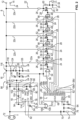
- FIG.1 A circuit 2 with a device 4 to be protected is shown in a simplified schematic, which is inserted into an electrical line 6.
- the electrical line 6 is electrically contacted with the device 4 to be protected, which is a mobile radio transponder.
- the circuit 2 also comprises an overvoltage protection 8, which is connected in parallel to the device 4 to be protected.
- the device 4 to be protected and the overvoltage protection 8 are arranged within a housing 10.
- the surge protector 8 has a first connection 12 and a second connection 14, which are directly electrically contacted with the electrical line 6, with the device 4 to be protected being located between the two connections 12, 14.
- the surge protector 8 has a detection circuit 16, by means of which an overvoltage can be detected which is present between the two connections 12, 14, for example due to a lightning strike.
- the surge protector 8 comprises a timer 18 and a shift register 20.
- the timer 18 is an NE555 component.
- the surge protector 8 has a number of strands 22 which are connected in parallel to one another and are each electrically contacted with the first connection 12 and the second connection 14. The strands 22 are thus connected in parallel to the device 4 to be protected.
- the detection circuit 16 detects the overvoltage present between the first connection 12 and the second connection 14, if it occurs. As a result, the timer 18, which is an NE555 component, is controlled.
- the shift register 20 is controlled by this and is thus supplied with certain clock pulses by means of the timer 18.
- the strands 22 are controlled by means of the shift register 20.
- the overvoltage protection 8 is based on analog technology. In other words, the strands 22 as well as the timer 18 as well as the shift register 20 and the detection circuit 16 are designed as analog components and thus consist of analog components.
- FIG. 2 A comparatively detailed circuit diagram of the overvoltage protection 8 with the strands 22 is shown.
- the overvoltage protection 8 has a first strand 22a, a second strand 22b, a third strand 22c, a fourth strand 22d and a fifth strand 22e, which are connected in parallel to one another and are led to the first connection 12 and to ground 24, to which the second connection 14 is also led.
- the strands 22 are thus connected in parallel to one another between the first connection 12 and the second connection 16.
- the strands 22 are identical in construction and each have a resistor 26 and a switching element 28 in the form of an IGBT. In summary, each of the strands 22 has one of the switching elements 28.
- the resistor 26 and the switching element 28 of each strand 22 are connected in series with one another.
- the ohmic resistance of the individual strands 22a, 22b, 22c, 22d, 22e is at least partially increased by an integer multiple.
- the ohmic resistance of the resistor 26 of the first strand 22a is 20 ohms
- the ohmic resistance of the resistor 26 of the second strand 22b is 40 ohms
- the ohmic resistance of the resistor 26 of the third strand 22c is 80 ohms
- the ohmic resistance of the resistor 26 of the fourth and fifth strands 22d, 22e is 160 ohms each.
- a series circuit of a further resistor 30 and a capacitor 32 is connected in parallel to the switching element 28 of the fifth strand 22e.
- the capacitor 32 is connected to the potential of the second connection 14, i.e. ground 24.
- the capacitor 32 itself is bridged by means of an additional resistor 34, which is consequently connected in parallel to the capacitor 32.
- the ohmic resistance of the further resistor 30 is equal to the ohmic resistance of the resistor 26 of the fifth strand 22e and is 160 ohms.
- the ohmic resistance of the additional resistor 34 is, for example, 1 MOhm.
- Each switching element 28 has a control input 36, by means of which the switching state of the respective switching element 28 can be set. If the switching element 28 is set by means of the control input 36 in such a way that it is in an electrically non-conductive state, a current flow via this same strand 22 is prevented.
- the overvoltage protection 8 has a first OR logic switch 40, a second OR logic switch 42, a third OR logic switch 44, a fourth OR logic switch 46 and a fifth OR logic switch 48, which are each OR gates.
- the control input 36 of the switching element 28 of the first strand 22a is led to an output 50 of the first OR logic switch 40.
- the control input 36 of the switching element 28 of the second strand 22b is led to the output 50 of the second OR logic switch 42.
- the control input 36 of the switching element 28 of the third strand 22c is led to the output 50 of the third OR logic switch 44.
- the control input 36 of the switching element 28 of the fourth strand 22d is led to the output 50 of the fourth OR logic switch 46.
- the control input 36 of the switching element 28 of the fifth strand 22e is led to the output 50 of the fifth OR logic switch 48.
- the output 50 of the first OR logic switch 40 is connected to a third input 52 of the second OR logic switch 42.
- the output 50 of the second OR logic switch 42 is connected to the third input 52 of the third OR logic switch 44, whose output 50 is connected to the third input 52 of the fourth OR logic switch 46.
- the output 50 of the fourth OR logic switch 46 is connected to the third input 52 of the fifth OR logic switch 48.
- the third inputs 52 of the OR logic switches 42, 44, 46, 48 are thus also each connected to a control input 36 of one of the switching elements 28.
- Each of the OR logic switches 40, 42, 44, 46, 48 further has a first input 54, which is connected to the first terminal 12 via the detection circuit 16 acting as a control circuit.
- Each of the OR logic switches 40, 42, 44, 46, 48 also has a second input 56, which is respectively connected to an output 58 of the shift register 20.
- the second input 56 of the first OR logic switch 40 is connected to a first output 58a of the shift register 20
- the second input 52 of the second OR logic switch 42 is connected to a second output 58b of the shift register
- the second input 52 of the third OR logic switch 44 is connected to a third output 58c of the shift register 20
- the second input 52 of the fourth OR logic switch 46 is connected to a fourth output 58d of the shift register 20
- the second input 52 of the fifth OR logic switch 48 is connected to a fifth output 58e of the shift register 20.
- the OR logic switches 40, 42, 44, 46 and 48 are identical in construction, whereby the third input 52 of the first OR logic switch 40 is not shown and is connected to ground 24. A level is present at the respective output 50 of the OR logic switches 40, 42, 44, 46, 48 when a level is present at at least one of the inputs 52, 54, 56.
- the shift register 20 has a start output 60 and an end output 62.
- the start output 60 of the shift register 20 is free and therefore not electrically contacted with any other electrical or electronic component.
- An end output 62 of the shift register 20 is connected to a reset input 66 of the shift register 20 via a first diode 64.
- the diode 64 only enables a current flow from the end output 62 to the reset input 66. If the shift register 20 is activated, the start output 60 is controlled first. Following this, the first output 58a, the second output 58b, the third output 58c, the fourth output 58d, the fifth output 58e and then the end output 62 are controlled, the control taking place depending on a control signal present at a time input 68 of the shift register 20.
- the start output 60 thus corresponds to the channel Q0, the first output 58a to the channel Q1, the second output 58b to the channel Q2 ... up to the end output 62, which corresponds to the channel Q6.
- the reset input 66 of the shift register 20 is connected via a second capacitor 70 to a voltage supply source 72, by means of which a direct voltage of 15 volts is provided.
- the reset input 66 is also connected via a second resistor 74 to ground 24.
- a second diode 76 is connected in parallel to the second resistor 74, by means of which a current flow from ground 24 to the reset input 66 is possible.
- the timer 18 is connected as a monostable flip-flop.
- a GND connection 78 of the timer 18 is connected to ground 24 and a supply voltage connection 80 of the timer 18 is connected to the voltage supply source 72.
- a control connection 82 of the timer 18 is connected via a third capacitor 84 to ground 24.
- a discharge connection 86 of the timer 18 is connected to a threshold connection 88 of the timer 18 and via a fourth capacitor 90 to ground 24.
- the discharge connection 86 and the threshold connection 88 are also connected to the voltage supply source 72 by means of a third resistor 92.
- a trigger connection 94 of the timer 18 is electrically contacted by means of a voltage divider 96 of the detection circuit 16 to the first connection 12 and the electrical potential of the second connection 16.
- the trigger connection 94 is connected to the first connection 12 by means of a fourth resistor 98 and to ground 24 by means of a fifth resistor 100.
- a time output 102 of the timer 40 is led to the trigger connection 94 by means of a third diode 104, allowing a current to flow from the time output 102 to the trigger connection 94.
- the time output 102 is also led to a second input 106 of a further OR logic switch 108, which is identical in construction to the first OR logic switch 40.
- a first input 110 of the further OR logic switch 108 is led to the first input 54 of the first OR logic switch 40, the first input 54 of the second OR logic switch 42, the first input 54 of the third OR logic switch 44, the first input 54 of the fourth OR logic switch 46 and the first input 54 of the fifth OR logic switch 48.
- An output 112 of the further OR logic switch 108 is connected to the time input 68 of the shift register 20.
- the timer 18 has a reset input 114 which is connected to the control input 36 of the switching element 28 of the fifth branch 22e such that the timer 18 is reset if the switching element 28 of the fifth branch 22e is in the electrically non-
- the detection circuit 16 has a capacitive voltage divider 116 with a fifth capacitor 118 and a sixth capacitor 120, which are connected in series between the first terminal 12 and ground 24.
- a fourth diode 122 is arranged in series between the fifth capacitor 118 and the sixth capacitor 120, and the fifth capacitor 118 is connected by means of a sixth resistor 124 and the sixth capacitor 120 by means of a seventh resistor 126.
- the sixth capacitor 120 is bridged by means of a fifth diode 128 and is connected to the voltage supply source 72 by means of a sixth diode 130.
- the electrical voltage dropping across the sixth capacitor 120 exceeds a certain limit value, so that the first, second, third, fourth and fifth OR logic switches 40, 42, 44, 46, 48 are controlled, which is why the switching elements 28 are transferred to the electrically conductive state.
- the maximum electrical voltage applied to the OR logic switches 40, 42, 44, 46, 48, 108 is set by means of the fifth and sixth diodes 128, 130.
- the fifth and sixth capacitors 118, 120 are discharged by means of the sixth resistor 124 and the seventh resistor 126.
- the fourth diode 122 ensures that the fifth capacitor 118 can only be discharged via the sixth resistor 126.
- a method 132 for operating the overvoltage protection 8 is shown.
- the overvoltage is detected. This is done by means of the detection circuit 16, specifically when the electrical voltage occurring across the sixth capacitor 120 exceeds the specific limit value.
- all switching elements 28 are closed so that the electrical voltage between the first connection 12 and ground 24, on which the second connection 14 is located, is reduced. In other words, a current flow via the strands 22 is possible.
- the switching elements 28 are closed by means of the first, second, third, fourth and fifth OR logic switches 40, 42, 44, 46, 48 as soon as the specific voltage is present across the sixth capacitor 120.
- the electrical voltage occurring across the voltage divider 96 is increased due to the overvoltage, and this electrical voltage is applied to the trigger connection 94. of the timer 18.
- a signal is also sent to the shift register 20 via the further OR logic switch 108, so that now it is no longer the start output 60 that is controlled, but the first output 58a.
- the switching elements 28 remain in the closed state due to the control of the first OR logic switch 40 and the connection of the third inputs 52 to the outputs 50 of the respective preceding OR logic switch 40, 42, 44, 46, 48, even if the electrical voltage that drops across the sixth capacitor 120 falls below the specific limit value.
- a pulse is output via the time output 102 in a third work step 138 and passed to the further OR logic switch 68.
- the second output 58b of the shift register 20 is now controlled and the switching element 28 of the first strand 22a is opened.
- the period between the start of the second work step 136 and the start of the third work step 138 defines in particular a certain time period.
- the third work step 138 is repeated until the fifth output 58e is activated.
- a fourth work step 140 is carried out and the end output 62 of the shift register 20 is activated.
- the reset input 66 of the shift register 20 is activated and the start output 60 is activated again.
- the switching element 28 of the fifth branch 22e is also set to the open state, so that the timer 18 is also set to the original state via the reset input 114.
- the remaining electrical voltage between the first connection 12 and the second connection 14 is reduced via the further resistor 30 and the capacitor 32 as well as the resistor 26 of the fifth branch 22e.
- the additional resistor 34 ensures that the capacitor 32 is subsequently discharged.
- the overvoltage protection 8 ensures that relatively frequently occurring overvoltages are reliably intercepted without wear and tear, with the maximum operating time of the overvoltage protection 8 being comparatively high. If an electrical overvoltage occurs on the device 4 to be protected, the strands 22 are activated and thus switched to electrical conduction. As a result, the overvoltage present on the device 4 to be protected is limited due to the parallel strands 22. In addition, the timer 18 and the shift register 20 are activated. The maximum overvoltage depends on the flowing electrical current and the ohmic resistance of the strands 22. In this way, a surge current can be safely discharged without damaging the device 4 to be protected.
- a forced pulse circuit is implemented.
- the minimum pulse width is specified by means of the third resistor 92 and the fourth capacitor 90.
- the discharge connection 86 of the timer 18 is a collector of a transistor that is internally connected to the time output 102. This is therefore blocked when the output is high and therefore has a level, and conducts when the output is low, which is why the fourth capacitor 90 is charged via the third resistor 92 when the time output 102 is high. This continues as long as the electrical voltage at the threshold output 88 is below 2/3 of the electrical operating voltage. Since a new interval can only begin when the electrical voltage at the trigger output 94 has fallen below 1/3 of the operating voltage, the time output (output) 102 is fed back to the trigger output 94 via the third diode 104.
- the detection circuit 16 comprises the fifth capacitor 118, the sixth capacitor 120, the fourth diode 122 and the sixth and seventh resistors 124, 126.
- the fifth and sixth capacitors 118, 120 form the capacitive voltage divider 116.
- the electrical voltage via the sixth capacitor 120 is passed directly to the further OR logic switch 108 and the first, second, third, fourth and fifth OR logic switches 40, 42, 44, 46, 48. As soon as this electrical voltage exceeds a certain trigger value, all strands 22 are put into the electrically conductive state. In order to avoid damage to the OR logic switches 40, 42, 44, 46, 48, 108, the maximum electrical voltage is limited by means of the fifth and sixth diodes 128, 130.
- the sixth and seventh resistors 124, 126 ensure that the fifth and sixth capacitors 118, 120 are safely discharged.
- the fourth diode 122 ensures that the sixth capacitor 120 cannot discharge via the fifth capacitor 118. This can only be done using the seventh resistor 126, which is why an extended duty cycle of the strands 22 is realized.
- the overvoltage protection 8 works as intended even with comparatively short overvoltages and in particular the method 132 is executed even if the timer 18, the shift register 20 and/or the OR logic switches 40, 42, 44, 46, 48, 108 have a certain delay time.
Landscapes
- Emergency Protection Circuit Devices (AREA)
- Protection Of Static Devices (AREA)
Description
- Die Erfindung betrifft sowohl einen Überspannungsschutz zur Absicherung eines zu schützenden Geräts, mit einem ersten Anschluss und mit einem zweiten Anschluss als auch eine Schaltung mit einem zu schützenden Gerät und mit einem Überspannungsschutz. Die Erfindung betrifft ferner die Verwendung eines Überspannungsschutzes sowie ein Verfahren zum Betrieb eines Überspannungsschutzes.
- Elektrische Geräte weisen üblicherweise eine elektrische Nennspannung auf, bei der diese betrieben werden. Sofern diese Nennspannung signifikant überstiegen wird, ist eine Beschädigung des elektrischen Geräts möglich. Ein Übersteigen der Nennspannung tritt beispielsweise aufgrund eines technischen Defekts des elektrischen Geräts oder eines sonstigen Bestandteils des Stromkreises auf, dessen Bestandteil das elektrische Gerät ist. Zur Absicherung des elektrischen Geräts gegenüber derartigen elektrischen Spannungen werden üblicherweise Sicherungen oder Schutzschalter verwendet.
- Ferner ist es erforderlich, dass elektrische Geräte gegen eine Überspannung gesichert werden, die beispielsweise aufgrund eines Blitzschlages in eine Leitung des Stromkreises oder das elektrische Gerät selbst entstehen. Auch ist es möglich, dass innerhalb des Stromkreises aufgrund einer induktiven Kopplung eines Bestandteils des Stromkreises mit einem Blitz eine derartige Überspannung entsteht. Zudem können aufgrund von elektromagnetischen Pulsen (EMP) oder aufgrund elektrostatischer Entladungen (ESD) sowie Schaltvorgängen in dem Stromkreis derartige Überspannungen entstehen, die zu einer Beschädigung des Geräts führen können. Derartige Überspannungen übersteigen in einem vergleichsweise großen Masse die Nennspannung. Auch entstehen die Überspannungen aufgrund externer Ereignisse und sind daher durch das elektrische Gerät nicht beeinflussbar und können deswegen nicht vermieden werden
- Zur Absicherung des elektrischen Geräts gegen Überspannungen wird ein Überspannungsschutz herangezogen, der parallel zu dem zu schützenden Gerät geschaltet wird. Der Überspannungsschutz selbst weist beispielsweise eine Funkenstrecke oder einen Varistor auf. Hierbei wird die Überspannung um das zu schützende Gerät herumgeleitet, wobei beispielsweise ein Lichtbogen erzeugt wird. Die Funkenstrecke und der Varistor unterliegen Alterungseffekten, sodass nach einer bestimmten Zeitdauer die elektrische Spannung variiert, ab der der Überspannungsschutz anspricht. Auch führen auftretende Überspannungen zu einem Verschleiß des Überspannungsschutzes. Infolgedessen ist nicht sichergestellt, dass sämtliche Überspannungen, die zu einer Beschädigung des Geräts führen könnten, stets mittels des Überspannungsschutzes abgefangen werden. Somit muss der Überspannungsschutz nach bestimmten Zeitspannen ausgetauscht werden, um eine bestimmungsgemäße Funktionsweise zu gewährleisten.
- Aus
DE 198 11 269 C1 ist eine Schaltungsanordnung mit einer Schutzschaltung bekannt. Hierbei sind bei einem Beispiel zu einer Steuerschaltung mehrere Stränge mit jeweils einem Widerstand und einem nachgeordneten Schaltelement parallel geschaltet. - Aus
WO 98/45919 A1 - Die nachveröffentlichte
WO 2018/041452 A1 , die somit Stand der Technik nach Art. 54 (3) EPÜ darstellt, zeigt eine Trennvorrichtung mit einem Schalter und mit einem parallel zu dem Schalter geschalteten Spannungsbegrenzer. Der Spannungsbegrenzer weist eine Anzahl an zueinander parallel geschalteten Strängen auf, wobei jeder Strang einen Widerstand aufweist. - In
US 7,561,394 B2 ist ein Überspannungsschutzsystem offenbart. Mehrere Stränge mit jeweils einem Widerstand und einem Schalter sind zueinander parallel geschaltet. - Der Erfindung liegt die Aufgabe zugrunde, einen besonders geeigneten Überspannungsschutz sowie eine besonders geeignete Schaltung als auch eine besonders geeignete Verwendung eines Überspannungsschutzes und ein besonders geeignetes Verfahren zum Betrieb eines Überspannungsschutzes anzugeben, wobei insbesondere eine Sicherheit erhöht und vorzugsweise Herstellungs- und/oder Betriebskosten gesenkt sind.
- Hinsichtlich des Überspannungsschutzes wird diese Aufgabe durch die Merkmale des Anspruchs 1, hinsichtlich der Schaltung durch die Merkmale des Anspruchs 7, hinsichtlich der Verwendung durch die Merkmale des Anspruchs 8 und hinsichtlich des Verfahrens durch die Merkmale des Anspruchs 9 erfindungsgemäß gelöst. Vorteilhafte Weiterbildungen und Ausgestaltungen sind Gegenstand der Unteransprüche.
- Der Überspannungsschutz dient der Absicherung eines zu schützenden Geräts, insbesondere der elektrischen Absicherung. Mit anderen Worten wird mittels des Überspannungsschutzes eine Überspannung an dem zu schützenden Gerät oder ein durch das zu schützende Gerät fließender Impulsstrom vermieden. Hierfür ist der Überspannungsschutz zweckmäßigerweise geeignet, vorgesehen und/oder eingerichtet. Die Überspannung/der Impulsstrom entsteht unabhängig von dem Überspannungsschutz und dem zu schützenden Gerät, insbesondere durch ein externes Ereignis, wie einen Blitzschlag. Die Überspannung/der Impulsstrom ist insbesondere derart, dass diese das zu schützenden Gerät beschädigen würde, und mittels des Überspannungsschutzes wird zweckmäßigerweise die an dem zu schützenden Gerät anliegende elektrische Spannung begrenzt. Vorzugsweise fungiert der Überspannungsschutz als Ableiter und ist beispielsweise ein Überspannungs- und/oder Blitzstromableiter.
- Die Überspannung ist beispielsweise eine Wechselspannung oder eine Gleichspannung, und/oder der Impuls-/Blitzstrom ist ein Gleichstrom oder ein Wechselstrom. Beispielsweise weist die Überspannung eine Frequenz größer 500 Hz, 800 Hz oder 900 Hz auf. Zweckmäßigerweise ist die Frequenz größer oder gleich 1 kHz, 1,5 kHz, 2 kHz, 5 kHz oder 10 kHz. Insbesondere ist die Frequenz kleiner oder gleich 10 MHz, 5 MHz oder 1 MHz. Insbesondere ist der Überspannungsschutz geeignet, bevorzugt vorgesehen und eingerichtet, einen Nennstrom zu tragen, der größer oder gleich 100 A, 300 A, 500 A, 800 A, 2 kA, 3 kA, 5 kA, 10 kA, 12 kA, 17 kA, 20 kA, 22 kA, 25 kA oder 30 kA ist. Unter tragbarem Strom wird insbesondere derjenige elektrische Strom verstanden, der mittels des Überspannungsschutzes geführt werden kann, ohne dass hierdurch eine Beschädigung hervorgerufen wird.
- Beispielsweise ist der Überspannungsschutz geeignet, insbesondere vorgesehen und eingerichtet, vor einer Überspannung zu schützen, die größer oder gleich 100 V, 200 V, 300 V, 400 V oder 500 V ist. Beispielsweise ist die maximale Überspannung 1.100 V, 1.000 V, 900 V oder 800 V, insbesondere sofern der elektrische Strom ein Wechselstrom ist. Sofern der elektrische Strom ein Gleichstrom ist, ist die maximale Überspannung geeigneterweise kleiner oder gleich 2.000 V, 1.800 V, 1.500 V, 1.200V oder 1.000 V.
- Mittels des Überspannungsschutzes wird beispielsweise ein Freiluftgerät abgesichert, also ein Gerät, welches im Außenbetrieb verwendet wird. Insbesondere ist das Gerät stationär. Beispielsweise ist das Gerät ein Transponder, wie ein Mobilfunktransponder. Derartige Mobilfunktransponder sind meistens an exponierten Positionen angeordnet und unterliegen daher der Gefahr eines Blitzschlages oder zumindest der Gefahr eines Ausgesetztseins einer Überspannung aufgrund eines Blitzschlages.
- Der Überspannungsschutz weist einen ersten Anschluss und einen zweiten Anschluss auf, von denen jeder im Montagezustand mit dem zu schützendes Gerät elektrisch kontaktiert ist. Im Überspannungsfall (Überspannungsereignis) liegt zwischen dem ersten Anschluss und dem zweiten Anschluss die Überspannung an.
- Zwischen den ersten Anschluss und den zweiten Anschluss ist eine Anzahl an Strängen zueinander parallel geschaltet. Mit anderen Worten sind die Stränge zueinander parallel geschaltet und jeweils mit dem ersten Anschluss und dem zweiten Anschluss elektrisch kontaktiert. Mit anderen Worten sind die beiden Anschlüsse mittels der Stränge elektrisch kontaktiert und das zu schützende Gerät ist vorzugsweise mittels der Stränge überbrückt.
- Jeder der Stränge weist einen Widerstand auf, und zumindest einer der Stränge umfasst ein Schaltelement, das in Reihe zu dem Widerstand des Strangs geschaltet ist. Mit anderen Worten weist dieser Strang den Widerstand und das Schaltelement auf, wobei das Schaltelement und der Widerstand in Reihe geschaltet sind. Diese Reihenschaltung ist im Montagezustand insbesondere parallel zu dem zu schützenden Gerät geschaltet. Die Widerstände der Stränge sind zweckmäßigerweise ohmsche Widerstände und weisen vorzugsweise einen Widerstand von mindestens 1 mOhm, 5 mOhm, 10 mOhm, 50 mOhm, 100 mOhm, 500 mOhm, 1 Ohm, 2 Ohm, 5 Ohm, 10 Ohm, 20 Ohm, 50 Ohm, 100 Ohm, 200 Ohm, 500 Ohm, 1 kOhm, 2 kOhm, 5 kOhm oder 10 kOhm auf. Der Widerstand ist bevorzugt kleiner oder gleich 1 kOhm, 500 Ohm oder 100 Ohm. Vorzugsweise umfasst der Überspannungsschutz 2 Stränge, 3 Stränge oder 5 Stränge. Insbesondere ist die Anzahl der Stränge größer oder gleich 2 Stränge, 3 Stränge oder 4 Stränge. Zum Beispiel ist die Anzahl der Stränge kleiner oder gleich 20 Stränge oder 10 Stränge.
- Mittels der Stränge wird die zwischen den beiden Anschlüssen anfallende elektrische Spannung begrenzt. Hierbei ist die elektrische Spannung vorzugsweise derart begrenzt, dass eine Beschädigung des zu schützenden Geräts unterbunden ist. Infolgedessen ist eine Sicherheit erhöht. Auch ist der Überspannungsschutz mittels einer vergleichsweise geringen Anzahl von kostengünstigen elektrischen Bauelementen realisierbar, was Herstellungskosten senkt. Auch unterliegen diese vergleichsweise geringen Alterungseffekten, sodass der Überspannungsschutz über einen vergleichsweise lange Zeitdauer einen sicheren Schutz vor einer bestimmten Überspannung gewährleistet. Mittels des Schaltelements ist es ermöglicht, einen Stromfluss in dem das Schaltelement aufweisenden Strang zu unterbinden und folglich den elektrischen Widerstand des Überspannungsschutzes einzustellen. Infolgedessen kann die über dem zu schützenden Gerät anfallende elektrische Spannung mittels des Überspannungsschutzes eingestellt und begrenzt werden, was eine Sicherheit erhöht. Auch kann der Überspannungsschutz für unterschiedliche Anforderungen herangezogen werden.
- Zweckmäßigerweise wird das Schaltelement in Abhängigkeit der Überspannung und/oder eines Impuls-/Blitzstroms betätigt. Geeigneterweise wird das Schaltelement in einen elektrischen leitenden Zustand versetzt, wenn die Überspannung bzw. der Impuls-/Blitzstrom erfasst wird, bzw. diese auftreten/anliegen. Zusammenfassend kann mittels des Schaltelements der elektrische Widerstand des Überspannungsschutzes angepasst werden, sodass eine über den Überspannungsschutz und somit zwischen den beiden Anschlüssen anfallende elektrische Spannung angepasst werden kann. Hierbei ist mittels der Anzahl der Stränge sowie mittels Wahl des jeweiligen Widerstands eine Skalierbarkeit des Überspannungsschutzes gegeben, sodass diese auf unterschiedlichste elektrische Spannungen und/oder elektrische Ströme angepasst werden kann. Folglich ist ein Einsatzbereich des Überspannungsschutzes vergrößert.
- Das Schaltelement ist insbesondere ein Halbleiterschaltelement, beispielsweise ein Transistor, wie ein Feldeffekttransistor, insbesondere ein MOSFET. Beispielsweise ist das Schaltelement ein Feldeffekttransistor, ein Sperrschicht-Feldeffekttransistor (JFET) oder ein MOSFET. Da die Überspannung auf die Stränge aufgeteilt ist, liegt an dem Schaltelement eine verringerte elektrische Spannung an, weswegen ein vergleichsweise kostengünstiges Schaltelement herangezogen werden kann.
- Jeder Strang weist ein derartiges Schaltelement auf. Hierbei sind die Schaltelemente der Stränge beispielsweise baugleich. Alternativ oder in Kombination hierzu sind die Schaltelemente auf den Widerstand des jeweiligen Strangs angepasst. Jeder Strang weist zusammenfassend sowohl den Widerstand als auch das Schaltelement auf, die zueinander in Reihe geschaltet sind. Aufgrund der Schaltelemente ist somit eine Skalierbarkeit des Überspannungsschutzes vergrößert, sodass der elektrische Widerstand des Überspannungsschutzes und folglich die zwischen den beiden Anschlüssen anliegende elektrische Spannung mittels der Schaltelemente eingestellt werden kann. Insbesondere sind die Stränge baugleich. Mit anderen Worten weisen sowohl sämtliche Widerstände den gleichen ohmschen Widerstand auf, und sämtliche Schaltelemente sind vom gleichen Typ. Zumindest jedoch sind die Stränge schaltungsgleich. Mit anderen Worten umfasst jeder Strang die gleiche Art an elektrischen und/oder elektronischen Bauteilen, wobei jedoch die jeweiligen Spezifikationen unterschiedlich sein können. Die elektrischen und/oder elektronischen Bauteile sind hierbei in der gleichen Art miteinander verschaltet. Geeigneterweise ist der ohmsche Widerstand der einzelnen Widerstände der Stränge unterschiedlich. Sofern der Überspannungsschutz eine Anzahl an Strängen aufweist, sind hierbei die Werte des ohmschen Widerstands vorzugsweise um jeweils ein bestimmtes konstantes Vielfaches erhöht. Das Vielfache ist insbesondere ein ganzzahliges Vielfaches und zum Beispiel zwei oder drei. Geeigneterweise weist somit jeweils einer der Stränge einen ohmschen Widerstand von 20 Ohm, 40 Ohm, 80 Ohm,... bzw. 20 Ohm, 60 Ohm, 180 Ohm,... auf, sofern der kleinste Widerstand jeweils einen ohmschen Widerstand von 20 Ohm aufweist. Auf diese Weise ist eine vergleichsweise präzise Einstellung der zwischen den zwei Anschlüssen anliegenden elektrischen Spannung ermöglicht. Zudem sind Herstellungskosten aufgrund der Verwendung von Gleichteilen reduziert.
- Jedes Schaltelement weist einen Steuereingang auf, mittels dessen eine Schaltstellung des Schaltelements beeinflusst werden kann. Mit anderen Worten wird mittels Ansteuerung des Steuereingangs der Schaltzustand des Schaltelements beeinflusst, und dieses folglich in einen leitenden oder einen elektrisch nicht leitenden Zustand versetzt. Das Schaltelement ist zweckmäßigerweise elektrisch leitend, sofern an dem Steuereingang ein Signal anliegt, also sofern dieses angesteuert wird. Der Steuereingang jedes der Schaltelemente ist gegen einen Ausgang jeweils eines Oder-Logikschalters geführt, insbesondere direkt. Mit anderen Worten ist der Steuereingang dieses Schaltelements elektrisch direkt bzw. signaltechnisch direkt mit dem Ausgang des jeweiligen Oder-Logikschalters kontaktiert.
- Jeder Oder-Logikschalter weist ferner einen ersten Eingang auf, der gegen den ersten Anschluss geführt ist, also mit dem ersten Anschluss verbunden ist. Hierbei ist der erste Eingang beispielsweise direkt oder über ein weiteres elektrisches und/oder elektronisches Bauteil gegen den ersten Anschluss geführt, insbesondere über eine Auslöseschaltung. Geeigneterweise weist der erste Eingang dann einen Pegel auf, wenn zwischen dem ersten Anschluss und dem zweiten Anschluss die Überspannung anliegt. Mit anderen Worten ist der erste Eingang derart mit dem ersten Anschluss verbunden, dass dieser den Pegel aufweist, wenn zwischen dem ersten Anschluss und dem zweiten Anschluss die Überspannung anliegt. Hierfür ist der erste Eingang beispielsweise zusätzlich mit dem zweiten Anschluss verbunden, insbesondere indirekt.
- Alternativ hierzu ist der Oder-Logikschalter über eine Erfassungsschaltung mit dem ersten Anschluss verbunden, wobei die Erfassungsschaltung derart ausgebildet und/oder eingestellt ist, dass bei der auftretenden Überspannung der erste Eingang den Pegel aufweist. Somit werden die Schaltelemente in elektrisch leitenden Zustand versetzt, falls die Überspannung anliegt. Infolgedessen sind sämtliche Stränge stromführend, und die zwischen den Anschlüssen anliegende elektrische Spannung ist aufgrund der Parallelschaltung der Stränge, die elektrisch leitend sind, begrenzt. Somit wird das zu schützende Gerät, welches parallel zu den Strängen geschaltet ist, vor der Überspannung geschützt.
- Der Überspannungsschutz weist ein Schieberegister auf, das eine Anzahl an Ausgängen aufweist, wobei die Anzahl der Ausgänge zweckmäßigerweise gleich der Anzahl der Schaltelemente ist. Bei Betrieb des Schieberegisters werden zweckmäßigerweise sukzessive die Ausgänge angesteuert, wobei insbesondere stets höchstens einer der Ausgänge zu jedem Zeitpunkt angesteuert ist. Ein zweiter Eingang jedes Oder-Logikschalters ist gegen jeweils einen der Ausgänge des Schieberegisters geführt, insbesondere direkt. Sofern an einem der Eingänge des jeweiligen Oder-Logikschalters ein Pegel anliegt, liegt vorzugsweise auch an dem Ausgang des jeweiligen Oder-Logikschalters ein Pegel an. Folglich ist der Oder-Logikschalter aktiv, sofern ein aktives Signal an einem dessen beider Eingänge anliegt. Lediglich, wenn weder an dem ersten noch an dem zweiten Eingang ein aktives Signal (Pegel) anliegt, ist auch der Ausgang des Oder-Logikschalters nicht aktiv. Die Oder-Logikschalter sind insbesondere baugleich und vorzugsweise Oder-Gatter.
- Wenn mittels des Schieberegisters das Ausgangssignal von einem der Ausgänge (erster Ausgang) zu einem anderen der Ausgänge (zweiter Ausgang) geschoben wird, wird insbesondere das Schaltelement, dessen Steuereingang mit dem ersten Ausgang kontaktiert ist, in den elektrisch nicht leitenden Zustand versetzt. Das Schaltelement hingegen, dessen Steuereingang mit dem zweiten Ausgang kontaktiert ist, bleibt vorzugsweise in einem elektrisch leitenden Zustand oder wird in den elektrisch leitenden Zustand versetzt. Infolgedessen ist der elektrische Widerstand des Überspannungsschutzes erhöht.
- Somit werden die Schaltelemente dann aktiviert, wenn entweder die Überspannung anliegt oder der jeweils zugeordnete Oder-Logikschalter mittels des Schieberegisters angesteuert wird. Insbesondere erfolgt ein Schließen sämtlicher Schaltelemente, sobald die Überspannung vorherrscht. Im Anschluss hieran wird zweckmäßigerweise das Schieberegister aktiviert, und sukzessive die Schaltelemente betätigt. Hierbei liegt zweckmäßigerweise die Überspannung nicht mehr zwischen den beiden Anschlüssen an, so dass mittels der Ansteuerung des Schieberegisters die Schaltelemente angesteuert werden. Mit anderen Worten liegt an dem ersten Eingang jedes Oder-Logikschalters kein Pegel mehr an, und lediglich über dem zweiten Eingang wird das Schaltelement angesteuert.
- Das Schieberegister weist zusammenfassend eine Anzahl an Ausgängen auf, von denen jeder mit einem Oder-Logikschalter verbunden ist, und die geeigneterweise nummeriert sind. Der erste Ausgang des Schieberegisters entspricht insbesondere einem Kanal 1, und der zweite Ausgang entspricht insbesondere einem Kanal 2. Besonders bevorzugt ist ein Startausgang des Schieberegisters frei. Der Startausgang entspricht insbesondere einem Kanal 0 und befindet sich vor dem ersten Ausgang. Insbesondere befindet sich der erste Ausgang zwischen dem Startausgang und dem zweiten Ausgang. Der Startausgang ist nicht belegt, und es ist kein elektrisches oder elektronisches Bauteil an diesem angeschlossen. Folglich ist der Startausgang elektrisch lose und kein weiteres oder elektronisches Bauteil ist mit diesem elektrisch kontaktiert. Folglich befinden sich im Normalzustand die Schaltelemente in dem elektrisch nicht leitenden Zustand, und der elektrische Widerstand des Überspannungsschutzes ist vergleichsweise groß. Daher ist bei einer Fehlfunktion des Schieberegisters oder sonstiger Bestandteile des Spannungsregisters ein ungewollter elektrischer Stromfluss über den Überspannungsschutz im Wesentlichen ausgeschlossen, auch wenn die zwischen den Anschlüssen anfallende elektrische Spannung vergleichsweise groß ist. Bei Aktivierung des Schieberegisters wird vorzugsweise der Startausgang angesteuert. Erst wenn das Schieberegister ein Signal erhält, wird die Ansteuerung des Startausgangs beendet und die Ansteuerung des ersten Ausgangs aufgenommen, sodass dann ein Pegel (Signal) an einem der Oder-Logikschalter anliegt.
- Zweckmäßigerweise umfasst das Schieberegister einen Reset-Eingang. Mittels einer Ansteuerung des Reset-Eingangs wird das Schieberegister in einen definierten Zustand gebracht. Insbesondere erfolgt eine Aktivierung des Startausgangs des Schieberegisters, sofern an dem Reset-Eingang ein Signal anliegt. Zweckmäßigerweise ist ein Endausgang des Schieberegisters gegen den Reset-Eingang geführt. Der Endausgang des Schieberegisters ist insbesondere derjenige Ausgang des Schieberegisters, der sich direkt neben einem Ausgang des Schieberegisters befindet, der gegen einen der Oder-Logikschalter geführt ist. Sofern folglich lediglich der erste oder zweite Eingang des Oder-Logikschalters belegt ist, also sofern lediglich zwei Schaltelemente mittels des Schieberegisters angesteuert werden, entspricht der Endausgang dem dritten Ausgang. Sofern folglich sukzessive die Anzahl der angesteuerten Schaltelemente reduziert wurde, wird der Endausgang des Schieberegisters angesteuert, und das Schieberegister wird folglich erneut in den ursprünglichen Zustand versetzt. Hierbei ist zweckmäßigerweise der Startausgang des Schieberegisters frei, sodass dieser zeitlich nachfolgend zu dem Endausgang angesteuert wird. Somit wird, sofern der Endausgang angesteuert wird, keines der Schaltelemente angesteuert, weswegen keiner der Stränge elektrisch leitend ist. Zweckmäßigerweise ist eine Diode zwischen dem Endausgang und dem Reset-Eingang geschaltet, was eine Beschädigung des Schieberegisters vermeidet. Zusammenfassend ist der Endausgang der letzte belegte Kanal des Schieberegisters.
- Alternativ oder besonders bevorzugt in Kombination hierzu ist eine Spannungsversorgungsquelle gegen den Reset-Eingang des Schieberegisters geführt, beispielsweise über einen Kondensator. Die Spannungsversorgungsquelle dient geeigneterweise dem Betrieb des Überspannungsschutzes. Die Spannungsversorgungsquelle selbst ist beispielsweise ein Kondensator, eine Batterie oder ein Transformator. Beispielsweise ist die Spannungsversorgungsquelle mit zumindest einem der Anschlüsse verschaltet, sodass die für den Betrieb des Überspannungsschutzes erforderliche elektrische Energie direkt einem Stromnetz entnommen wird, in das das zu schützende Gerät integriert ist.
- Das Schieberegister umfasst einen Zeit-Eingang. Bei Ansteuerung des Zeit-Eingangs des Schieberegisters werden sukzessive die Ausgänge des Schieberegisters durchgesteuert. Hierbei wird jedes Mal dann, wenn an dem Zeit-Eingang ein Signal anliegt, die Ansteuerung der Ausgänge derart verändert, dass diese um einen Ausgang weitergeschaltet werden. Der Zeit-Eingang des Schieberegisters ist gegen einen Ausgang eines weiteren Oder-Logikschalters geführt, insbesondere direkt. Der weitere Oder-Logikschalter weist einen ersten Eingang und einen zweiten Eingang auf. Somit wird, wenn an dem ersten Eingang oder dem zweiten Eingang ein Pegel anliegt, insbesondere die Ansteuerung der Ausgänge des Schieberegisters verändert. Der Pegel bezeichnet insbesondere ein Signal, welches verschieden von null (0) ist.
- Der Überspannungsschutz umfasst einen Zeitgeber mit einem Zeit-Ausgang. Der Zeit-Ausgang ist mit dem Zeit-Eingang des Schieberegisters wirkverbunden. Folglich wird mittels des Zeitgebers das Schieberegister angesteuert, wobei mittels des Zeitgebers vorzugsweise ein bestimmtes Taktsignal bereitgestellt wird, welches insbesondere eine konstante Periode aufweist, oder welches vorzugsweise von der aktuell anliegenden Überspannung abhängt. Beispielsweise ist der Zeit-Ausgang direkt mit dem Zeit-Eingang des Schieberegisters verbunden. Der Zeit-Ausgang ist gegen den zweiten Eingang des weiteren Oder-Logikschalters geführt, insbesondere direkt. An dem Zeit-Ausgang des Zeitgebers wird zweckmäßigerweise periodisch ein Ansteuersignal bereitgestellt.
- Der erste Eingang jedes Oder-Logikschalters ist gegen den ersten Eingang des weiteren Oder-Logikschalters geführt, insbesondere direkt. Mit anderen Worten ist der erste Eingang des weiteren Oder-Logikschalters mit dem ersten Anschluss wirkverbunden. Somit weist geeigneterweise der Ausgang des weiteren Oder-Logikschalters dann einen Pegel auf, wenn die Überspannung auftritt oder mittels des Zeitgebers ein Signal bereitgestellt ist.
- Insbesondere ist der Steuereingang eines der Schaltelemente mit einem Reset-Anschluss des Zeitgebers verbunden. Solange ein Signal an dem Reset-Anschluss des Zeitgebers anliegt, wird dieser insbesondere in einem Grund- oder Startzustand gehalten. Zweckmäßigerweise ist die Verbindung derart, dass ein Reset erfolgt, wenn das Schaltelement geöffnet ist. Somit wird das Schieberegister lediglich dann weitergezählt, wenn das Schaltelement, oder zumindest eines der Schaltelemente, in einem geschlossenen Zustand ist. Geeigneterweise ist die Verschaltung des Überspannungsschutzes derart, dass nach Erfassen der Überspannung sämtliche Schaltelemente in den elektrisch leitenden Zustand versetzt werden, und dass der Zeitgeber aktiviert wird. Hierbei werden mittels des Schieberegisters geeigneterweise die Oder-Logikschalter sukzessive aktiviert, so dass die Schaltelemente in den elektrisch nicht-leitenden Zustand überführt werden. Sobald das letzte elektrisch leitende Schaltelement in den elektrisch nicht-leitenden Zustand überführt wird, wird zweckmäßigerweise der Zeitgeber zurückgesetzt.
- Beispielsweise ist der Zeitgeber ein NE555. Geeigneterweise ist "OUT" der Zeit-Ausgang, der beispielsweise gegen den Logikschalter oder direkt gegen den Zeit-Eingang des Schieberegisters direkt oder indirekt über den weiteren Oder-Logikschalter geführt ist. Insbesondere ist "OUT'" mittels einer Diode gegen den "TRIG" (Trigger-Anschluss) geführt, welcher insbesondere mittels eines Widerstandsteilers gegen den ersten Anschluss geführt ist, welcher bei Betrieb vorzugsweise ein elektrisches Potential aufweist, das verschieden von null (0) ist. Beispielsweise ist "GND" (GND-Anschluss) gegen den zweiten Anschluss des Überspannungsschutzes geführt. Beispielsweise ist "RESET" (Reset-Anschluss) mit dem Steuereingang eines der Schaltelemente wirkverbunden, beispielsweise direkt dagegen geführt. Zweckmäßigerweise ist der NE555 als monostabile Kippstufe realisiert.
- Zumindest einer der Oder-Logikschalter weist einen dritten Eingang auf, wobei an dem Ausgang des Oder-Logikschalters zweckmäßigerweise genau dann ein Pegel anliegt, wenn an zumindest einem der drei Eingänge ein Pegel anliegt. Insbesondere weisen sämtliche Oder-Logikschalter den dritten Eingang auf. Hierbei ist beispielsweise bei einem der Oder-Logikschalter der dritte Eingang auf Masse gelegt. Der dritte Eingang zumindest eines der Oder-Logikschalter ist gegen einen Ausgang eines der anderen der Oder-Logikschalter geführt, insbesondere direkt. Vorzugsweise ist hierbei der dritte Eingang gegen den Steuereingang eines der Schaltelemente geführt, welcher ebenfalls gegen den Ausgang des anderen der Oder-Logikschalter geführt ist. Geeigneterweise sind mit Ausnahme eines der Oder-Logikschalter sämtliche dritte Eingänge gegen jeweils einen Ausgang eines weiteren der Oder-Logikschalter geführt, und jedem Ausgang der Oder-Logikschalter ist somit einer der dritten Eingänge der Oder-Logikschalter zugeordnet.
- Falls mittels des Schieberegisters somit einer der Oder-Logikschalter aktiviert wird, wird dieser Oder-Logikschalter und ein anderer der Oder-Logikschalter über dessen Ausgang aktiviert. Somit sind zumindest zwei der Schaltelemente aktiviert und elektrisch leitend geschaltet, weswegen zumindest zwei der Stränge des Überspannungsschutzes elektrisch leitend sind. Insbesondere ist die Verschaltung derart, dass bei Ansteuerung eines der Oder-Logikschalter sämtliche Schaltelemente in den elektrisch leitenden Zustand versetzt werden. Dieser Oder-Logikschalter ist bevorzugt gegen den ersten Ausgang des Schieberegisters geführt. Somit erfolgt die Ansteuerung sämtlicher Schaltelemente zweckmäßigerweise dann, wenn der erste Ausgang des Schieberegisters angesteuert wird. Sobald der nachfolgende Ausgang des Schieberegisters angesteuert wird, wird vorzugsweise lediglich eines der Schaltelemente in den elektrisch nicht-leitenden Zustand überführt, so dass die Anzahl der elektrisch leitenden Stränge des Überspannungsschutzes um genau eins (1) reduziert ist. Bei erneuter Ansteuerung des Schieberegisters und Ansteuerung eines weiteren der Ausgänge des Schieberegisters wird geeigneterweise aufgrund der Verschaltung der Oder-Logikschalter wiederum zusätzlich lediglich ein einziges der Schaltelemente in den elektrisch nicht-leitenden Zustand versetzt, so dass ein weiterer der Stränge des Überspannungsschutzes elektrisch nicht leitend ist. Infolgedessen ist es ermöglicht, mittels Ansteuerung des Schieberegisters den elektrischen Widerstand des Überspannungsschutzes sukzessive und stufenweise zu erhöhen.
- Vorzugsweise ist parallel zu dem Schaltelement eine Reihenschaltung eines weiteren Widerstands und einer Kapazität geschaltet. Sofern der Überspannungsschutz eine Anzahl derartiger Schaltungselemente aufweist, deren Steuereingang jeweils über einen Oder-Logikschalter zu einem Ausgang des etwaigen Schieberegisters geführt ist, ist vorzugsweise die Reihenschaltung parallel zu demjenigen Schaltelement geschaltet, welches gegen den Ausgang des Schieberegisters geführt ist, der benachbart zu dem Endausgang ist. Die Kapazität ist bevorzugt ein Kondensator. Sofern das Schaltelement in dem elektrisch nicht leitenden Zustand ist, ist mittels des Widerstands dieses Strangs sowie des weiteren Widerstands und der Kapazität ein RC-Kreis gebildet, welcher einen etwaigen weiter fließenden elektrischen Strom aufnimmt. Somit ist stets ein elektrischer Stromfluss über den Überspannungsschutz ermöglicht, auch wenn der elektrische Widerstand vergleichsweise groß ist. Zweckmäßigerweise ist der weitere Widerstand vergleichsweise groß, sodass der elektrische Strom gegen null (0) geführt wird. Aufgrund der Stränge des Überspannungsschutzes ist der fließende elektrische Strom vergleichsweise gering, sodass die Kapazität vergleichsweise klein dimensioniert werden kann, was Herstellungskosten reduziert. Geeigneterweise ist zur Kapazität ein zusätzlicher Widerstand parallel geschaltet. Mittels des zusätzlichen Widerstands ist sichergestellt, dass die Kapazität stets entladen wird.
- Zweckmäßigerweise basiert der Überspannungsschutz auf Analogtechnik. Mit anderen Worten ist der Überspannungsschutz in Analogtechnik erstellt. Sofern der Überspannungsschutz folglich die Oder-Logikschalter, den Zeitgeber, den weiteren Oder-Logikschalter und/oder das Schieberegister aufweist, basieren diese insbesondere auf Analogtechnik und sind in dieser gefertigt. Auf diese Weise ist eine Robustheit erhöht. Zudem sind Herstellungskosten reduziert.
- Die Schaltung weist ein zu schützendes Gerät auf, dem ein Überspannungsschutz parallel geschaltet ist. Das zu schützende Gerät ist zweckmäßigerweise ein Freilandgerät, wie beispielsweise ein Transponder. Insbesondere ist das zu schützende Gerät für eine Funkkommunikation vorgesehen und beispielsweise ein Mobilfunktransponder. Der Überspannungsschutz weist einen ersten Anschluss und einen zweiten Anschluss auf, zwischen denen eine Anzahl an Strängen zueinander parallel geschaltet ist, wobei jeder Strang einen Widerstand aufweist, und wobei zumindest einer der Stränge ein Schaltelement umfasst, das in Reihe zu dem Widerstand des Strangs geschaltet ist. Das zu schützende Gerät ist sowohl mit dem ersten Anschluss als auch mit dem zweiten Anschluss des Überspannungsschutzes elektrisch kontaktiert. Die Schaltung ist beispielsweise innerhalb eines Gehäuses integriert oder weist ein Gehäuse auf, sodass das Gerät und der Überspannungsschutz mittels des gemeinsamen Gehäuses vor mechanischen Einflüssen geschützt werden. Alternativ hierzu umfassen das zu schützende Gerät und der Überspannungsschutz jeweils ein separates Gehäuse, welche beispielsweise zur Montage aneinander befestigt werden.
- Ein Überspannungsschutz, der einen ersten Anschluss und einen zweiten Anschluss aufweist, zwischen denen eine Anzahl an Strängen zueinander parallel geschaltet sind, wobei jeder Strang einen Widerstand aufweist, und wobei zumindest einer der Stränge ein Schaltelement umfasst, das in Reihe zu dem Widerstand des Stranges geschaltet ist, wird zur Absicherung eines zu schützenden Geräts gegen eine Überspannung und/oder einen Impulsstrom verwendet. Hierbei tritt insbesondere aufgrund eines Blitzschlages die Überspannung zwischen dem ersten und dem zweiten Anschluss des Überspannungsschutzes auf. Der Blitzschlag erfolgt hierbei beispielsweise in eine direkt mit dem ersten Anschluss bzw. mit dem zweiten Anschluss elektrisch kontaktierten Leitung, oder die Überspannung tritt aufgrund einer Kopplung eines aufgrund des Blitzschlags hervorgerufenen Magnetfelds mit der Leitung auf.
- Das Verfahren dient dem Betrieb eines Überspannungsschutzes zur Absicherung eines zu schützenden Geräts, mit einem ersten Anschluss und mit einem zweiten Anschluss, zwischen denen eine Anzahl an Strängen zueinander parallel geschaltet ist. Jeder Strang weist einen Widerstand auf, und zumindest einer der Stränge umfasst ein Schaltelement, das in Reihe zu dem Widerstand des Strangs geschaltet ist. Das Verfahren sieht vor, dass eine Überspannung erfasst wird. Die Überspannung ist eine elektrische Spannung und liegt beispielsweise zwischen dem ersten Anschluss und dem zweiten Anschluss an. Die Überspannung ist hierbei insbesondere derart, dass ein mittels des Überspannungsschutzes zu schützendes Gerät aufgrund der Überspannung beschädigt würde. Die Überspannung tritt beispielweise aufgrund eines Impulsstroms und/oder einer induktiven Wirkung auf. Alternativ oder in Kombination hierzu tritt die Überspannung aufgrund eines Blitzschlages auf. Die Überspannung wird beispielsweise mittels eines externen Geräts, eines Sensors, oder intrinsisch mittels des Überspannungsschutzes selbst erfasst. Die Erfassung der Überspannung erfolgt geeigneterweise qualitativ oder quantitativ. Nach dem Erfassen der Überspannung wird das Schaltelement für eine Zeitspanne geschlossen. Geeigneterweise wird das Schaltelement im Wesentlichen unverzüglich nach Erfassen oder bei Erfassen der Überspannung geschlossen.
- Somit kommutiert bei Auftreten der Überspannung der elektrische Strom zumindest teilweise auf den Überspannungsschutz und zwar auf die Stränge. Aufgrund der Parallelschaltung der Widerstände ist der elektrische Widerstand des Überspannungsschutzes verringert. Nach Ablauf der Zeitspanne, die insbesondere in Abhängigkeit der aktuell anliegenden Überspannung festgelegt ist, wird das Schaltelement geöffnet, was zu einer Erhöhung des elektrischen Widerstands des Überspannungsschutzes führt. Sofern der Überspannungsschutz eine Anzahl an Strängen mit Schaltelementen aufweist, sieht das Verfahren vor, dass diese sukzessive geöffnet werden, wobei sämtliche Schaltelemente zweckmäßigerweise beim Erfassen der Überspannung zunächst geschlossen werden. Geeigneterweise ist zwischen Betätigung der einzelnen Schaltelemente jeweils eine oder die Zeitspanne vorhanden, sodass der elektrische Widerstand des Überspannungsschutzes sukzessive erhöht wird.
- Wenn mittels des Überspannungsschutzes ein Gerät vor einem Impulsstrom und/oder einer Überspannung wird, das parallel zu dem Überspannungsschutz geschaltet ist, ist die über das Gerät anfallende elektrische Spannung begrenzt. Nach Ablauf der Zeitspanne ist der fließende elektrische Strom aufgrund des elektrischen Widerstands des Überspannungsschutzes reduziert. Wenn nun das Schaltelement betätigt wird, steigt der elektrische Widerstand und folglich die elektrische Spannung erneut an. Dies führt zu einer weiteren und ausgeprägten Verringerung des elektrischen Stromflusses. Somit wird mittels Erhöhung des elektrischen Widerstands der elektrische Stromfluss sukzessive unterbunden, wobei die maximal anliegende elektrische Spannung reduziert ist. Sofern dem Schaltelement die Kapazität und der weitere Widerstand parallel geschaltet ist, wird mittels dieser Reihenschaltung nach Betätigung des Schaltelements ein etwaiger verbleibender elektrischer Stromfluss aufgenommen und gegen null gebracht.
- Sofern einzelne Bauteile als erstes, zweites, drittes... Bauteil bezeichnet werden, dient dies insbesondere lediglich der Bezeichnung des jeweiligen Bauteils. Insbesondere impliziert dies nicht das Vorhandensein einer bestimmten Anzahl von Bauteilen. Die im Zusammenhang mit dem Überspannungsschutz und/oder der Schaltung genannten Vorteile und Weiterbildungen sind sinngemäß auch auf die Verwendung und das Verfahren zu übertragen und umgekehrt.
- Nachfolgend wird ein Ausführungsbeispiel der Erfindung anhand einer Zeichnung näher erläutert. Darin zeigen:
- Fig. 1
- schematisch vereinfacht eine Schaltung mit einem zu schützenden Gerät und einem Überspannungsschutz,
- Fig. 2
- einen Schaltplan des Überspannungsschutzes, und
- Fig. 3
- ein Verfahren zum Betrieb des Überspannungsschutzes.
- Einander entsprechende Teile sind in sämtlichen Figuren mit den gleichen Bezugszeichen versehen.
- In
Fig. 1 ist schematisch vereinfacht eine Schaltung 2 mit einem zu schützenden Gerät 4 dargestellt, welches in eine elektrische Leitung 6 eingebracht ist. Die elektrische Leitung 6 ist elektrisch mit dem zu schützenden Gerät 4 kontaktiert, das ein Mobilfunktransponder ist. Ferner umfasst die Schaltung 2 einen Überspannungsschutz 8, der parallel zu dem zu schützenden Gerät 4 geschaltet ist. Das zu schützende Gerät 4 sowie der Überspannungsschutz 8 sind innerhalb eines Gehäuses 10 angeordnet. - Der Überspannungsschutz 8 weist einen ersten Anschluss 12 sowie einen zweiten Anschluss 14 auf, die elektrisch direkt mit der elektrischen Leitung 6 kontaktiert sind, wobei sich das zu schützende Gerät 4 zwischen den beiden Anschlüssen 12, 14 befindet. Zudem weist der Überspannungsschutz 8 eine Erfassungsschaltung 16 auf, mittels derer eine Überspannung erfasst werden kann, welche zwischen den beiden Anschlüssen 12, 14 anliegt, beispielsweise aufgrund eines Blitzeinschlag. Zudem umfasst der Überspannungsschutz 8 einen Zeitgeber 18 sowie ein Schieberegister 20. Der Zeitgeber 18 ist ein NE555-Baustein. Zudem weist der Überspannungsschutz 8 eine Anzahl an Strängen 22 auf, die zueinander parallel geschaltet und jeweils mit dem ersten Anschluss 12 und dem zweiten Anschluss 14 elektrisch kontaktiert sind. Somit sind die Stränge 22 parallel zu dem zu schützenden Gerät 4 geschaltet.
- Mittels der Erfassungsschaltung 16 wird die zwischen dem ersten Anschluss 12 und dem zweiten Anschluss 14 anliegende Überspannung erfasst, sofern diese auftritt. Infolgedessen wird der Zeitgeber 18 angesteuert, der ein NE555-Baustein ist. Mittels dessen wird das Schieberegister 20 angesteuert und somit mittels des Zeitgebers 18 mit bestimmten Takten versorgt. Mittels des Schieberegisters 20 werden die Stränge 22 gesteuert. Der Überspannungsschutz 8 basiert auf Analogtechnik. Mit anderen Worten sind die Stränge 22 sowie der Zeitgeber 18 als auch das Schieberegister 20 und die Erfassungsschaltung 16 als Analog-Bauteile ausgeführt und bestehen somit aus analogen Bauteilen.
- In
Fig. 2 ist ein vergleichsweise detaillierter Schaltplan des Überspannungsschutzes 8 mit den Strängen 22 dargestellt. Der Überspannungsschutz 8 weist einen ersten Strang 22a, einen zweiten Strang 22b, einen dritten Strang 22c, einen vierten Strang 22d sowie einen fünften Strang 22e auf, die zueinander parallel geschaltet und gegen den ersten Anschluss 12 sowie gegen Masse 24 geführt sind, gegen die auch der zweite Anschluss 14 geführt ist. Somit sind die Stränge 22 zwischen dem ersten Anschluss 12 und dem zweiten Anschluss 16 zueinander parallel geschaltet. Die Stränge 22 sind baugleich und weisen jeweils einen Widerstand 26 sowie ein Schaltelement 28 in Form eines IGBTs auf. Zusammenfassend weist jeder der Stränge 22 jeweils eines der Schaltelemente 28 auf. Der Widerstand 26 und das Schaltelement 28 jedes Strangs 22 sind zueinander in Reihe geschaltet. Der ohmsche Widerstand der einzelnen Stränge 22a, 22b, 22c, 22d, 22e ist zumindest teilweise um jeweils ein ganzzahliges Vielfaches erhöht. Der ohmsche Widerstand des Widerstands 26 des ersten Strangs 22a beträgt 20 Ohm, der ohmsche Widerstand des Widerstands 26 des zweiten Strangs 22b beträgt 40 Ohm, der ohmsche Widerstand des Widerstands 26 des dritten Strangs 22c beträgt 80 Ohm, und der ohmsche Widerstand des Widerstands 26 des vierten und des fünften Strangs 22d, 22e beträgt jeweils 160 Ohm. - Parallel zu dem Schaltelement 28 des fünften Strangs 22e ist eine Reihenschaltung eines weiteren Widerstandes 30 und einer Kapazität 32 in Form eines Kondensators geschaltet. Hierbei ist der Kondensator 32 gegen das Potential des zweiten Anschluss 14 geführt, also Masse 24. Die Kapazität 32 selbst ist mittels eines zusätzlichen Widerstands 34 überbrückt, der folglich parallel zu der Kapazität 32 geschaltet ist. Der ohmsche Widerstand des weiteren Widerstands 30 ist gleich dem ohmsche Widerstand des Widerstands 26 des fünften Strangs 22e und beträgt 160 Ohm. Der ohmsche Widerstand des zusätzlichen Widerstands 34 beträgt beispielsweise 1 MOhm.
- Jedes Schaltelement 28 weist einen Steuereingang 36 auf, mittels dessen der Schaltzustand des jeweiligen Schaltelements 28 eingestellt werden kann. Sofern das Schaltelement 28 mittels des Steuereingangs 36 derart eingestellt ist, dass dieses in einem elektrisch nicht leitenden Zustand ist, ist ein Stromfluss über eben diesen Strang 22 unterbunden. Der Überspannungsschutz 8 weist einen ersten Oder-Logikschalter 40, einen zweiten Oder-Logikschalter 42, einen dritten Oder-Logikschalter 44, einen vierten Oder-Logikschalter 46 sowie einen fünften Oder-Logikschalter 48 auf, die jeweils Oder-Gatter sind. Der Steuereingang 36 des Schaltelements 28 des ersten Strangs 22a ist gegen einen Ausgang 50 des ersten Oder-Logikschalters 40 geführt. Der Steuereingang 36 des Schaltelements 28 des zweiten Strangs 22b ist gegen den Ausgang 50 des zweiten Oder-Logikschalters 42 geführt. Der Steuereingang 36 des Schaltelements 28 des dritten Strangs 22c ist gegen den Ausgang 50 des dritten Oder-Logikschalters 44 geführt. Der Steuereingang 36 des Schaltelements 28 des vierten Strangs 22d ist gegen den Ausgang 50 des vierten Oder-Logikschalters 46 geführt. Der Steuereingang 36 des Schaltelements 28 des fünften Strang 22e ist gegen den Ausgang 50 des fünften Oder-Logikschalters 48 geführt.
- Der Ausgang 50 des ersten Oder-Logikschalters 40 ist gegen einen dritten Eingang 52 des zweiten Oder-Logikschalters 42 geführt. Der Ausgang 50 des zweiten Oder-Logikschalters 42 ist gegen den dritten Eingang 52 des dritten Oder-Logikschalters 44 geführt, dessen Ausgang 50 gegen den dritten Eingang 52 des vierten Oder-Logikschalters 46 geführt ist. Der Ausgang 50 des vierten Oder-Logikschalters 46 ist gegen den dritten Eingang 52 des fünften Oder-Logikschalters 48 geführt. Somit sind auch die dritten Eingänge 52 der Oder-Logikschalter 42, 44, 46, 48 mit jeweils einem Steuereingang 36 eines der Schaltelemente 28 kontaktiert. Jeder der Oder-Logikschalter 40, 42, 44, 46, 48 weist ferner einen ersten Eingang 54 auf, welcher über die als Ansteuerschaltung fungierende Erfassungsschaltung 16 mit dem ersten Anschluss 12 verbunden ist. Auch weist jeder der Oder-Logikschalter 40, 42, 44, 46, 48 jeweils einen zweiten Eingang 56 auf, der jeweils gegen einen Ausgang 58 des Schieberegisters 20 geführt ist. So ist der zweite Eingang 56 des ersten Oder-Logikschalters 40 gegen einen ersten Ausgang 58a des Schieberegisters 20, der zweite Eingang 52 des zweiten Oder-Logikschalters 42 gegen einen zweiten Ausgang 58b des Schieberegisters 20, der zweite Eingang 52 des dritten Oder-Logikschalters 44 gegen einen dritten Ausgang 58c des Schieberegisters 20, der zweite Eingang 52 des vierten Oder-Logikschalters 46 gegen einen vierten Ausgang 58d des Schieberegisters 20 und der zweite Eingang 52 des fünften Oder-Logikschalters 48 gegen einen fünften Ausgang 58e des Schieberegisters 20 geführt.
- Die Oder-Logikschalter 40, 42, 44, 46 und 48 sind baugleich, wobei der dritte Eingang 52 des ersten Oder-Logikschalters 40 nicht dargestellt und gegen Masse 24 geführt ist. An dem jeweiligen Ausgang 50 der Oder-Logikschalter 40, 42, 44, 46, 48 liegt dann ein Pegel an, wenn an zumindest einem der Eingänge 52, 54, 56 ein Pegel anliegt.
- Zudem weist das Schieberegister 20 einen Startausgang 60 sowie einen Endausgang 62 auf. Der Startausgang 60 des Schieberegisters 20 ist frei und folglich mit keinem weiteren elektrischen oder elektronischen Bauteil elektrisch kontaktiert. Ein Endausgang 62 des Schieberegisters 20 ist über eine erste Diode 64 gegen einen Reset-Eingang 66 des Schieberegisters 20 geführt. Hierbei ist mittels der Diode 64 lediglich ein Stromfluss von dem Endausgang 62 zu dem Reset-Eingang 66 ermöglicht. Sofern das Schieberegister 20 aktiviert ist, wird zunächst der Startausgang 60 angesteuert. Im Anschluss hieran wird der erste Ausgang 58a, der zweite Ausgang 58b, der dritte Ausgang 58c, der vierte Ausgang 58d, der fünfte Ausgang 58e und im Anschluss hieran der Endausgang 62 angesteuert, wobei die Ansteuerung in Abhängigkeit eines an einem Zeit-Eingang 68 des Schieberegisters 20 anliegenden Ansteuersignals erfolgt. Der Startausgang 60 entspricht somit dem Kanal Q0, der erste Ausgang 58a dem Kanal Q1, der zweite Ausgang 58b dem Kanal Q2 ... bis zu dem End-Ausgang 62, der dem Kanal Q6 entspricht.
- Der Reset-Eingang 66 des Schieberegisters 20 ist über einen zweiten Kondensator 70 gegen eine Spannungsversorgungsquelle 72 geführt, mittels derer eine Gleichspannung von 15 Volt bereitgestellt ist. Auch ist der Reset-Eingang 66 über einen zweiten Widerstand 74 gegen Masse 24 geführt. Dem zweiten Widerstand 74 ist parallel eine zweite Diode 76 geschaltet, mittels derer ein Stromfluss von Masse 24 zu dem Reset-Eingang 66 ermöglicht ist.
- Der Zeitgeber 18 ist als monostabile Kippstufe verschaltet. So sind ein GND-Anschluss 78 des Zeitgebers 18 gegen Masse 24 und ein Versorgungsspannungsanschluss 80 des Zeitgebers 18 gegen die Spannungsversorgungsquelle 72 geführt. Ein Control-Anschluss 82 des Zeitgebers 18 ist über einen dritten Kondensator 84 gegen Masse 24 geführt. Ein Discharge-Anschluss 86 des Zeitgebers 18 ist gegen eine Threshold-Anschluss 88 des Zeitgebers 18 sowie über einen vierten Kondensator 90 gegen Masse 24 geführt. Auch sind der Discharge-Anschluss 86 und der Threshold-Anschluss 88 mittels eines dritten Widerstands 92 gegen die Spannungsversorgungsquelle 72 geführt. Ein Trigger-Anschluss 94 des Zeitgebers 18 ist mittels eines Spannungsteilers 96 der Erfassungsschaltung 16 mit dem ersten Anschluss 12 und dem elektrischen Potential des zweiten Anschlusses 16 elektrisch kontaktiert. Hierfür ist der Trigger-Anschluss 94 mittels eines vierten Widerstands 98 gegen den ersten Anschluss 12 und mittels eines fünften Widerstands 100 gegen Masse 24 geführt.
- Ein Zeit-Ausgang 102 des Zeitgebers 40 ist mittels einer dritten Diode 104 zu dem Trigger-Anschluss 94 geführt, wobei ein Stromfluss von dem Zeit-Ausgang 102 zu dem Trigger-Anschluss 94 ermöglicht ist. Der Zeit-Ausgang 102 ist ferner gegen einen zweiten Eingang 106 eines weiteren Oder-Logikschalters 108 geführt, der baugleich zu dem ersten Oder-Logikschalter 40 ist. Ein erster Eingang 110 des weiteren Oder-Logikschalters 108 ist gegen den ersten Eingang 54 des ersten Oder-Logikschalters 40, den ersten Eingang 54 des zweiten Oder-Logikschalters 42, den ersten Eingang 54 des dritten Oder-Logikschalters 44, den ersten Eingang 54 des vierten Oder-Logikschalters 46 sowie den ersten Eingang 54 des fünften Oder-Logikschalters 48 geführt. Ein Ausgang 112 des weiteren Oder-Logikschalters 108 ist gegen den Zeit-Eingang 68 des Schieberegisters 20 geführt ist. Ferner weist der Zeitgeber 18 einen Reset-Eingang 114 auf, der mit dem Steuereingang 36 des Schaltelements 28 des fünften Strangs 22e derart verschaltet ist, dass der Zeitgeber 18 zurückgesetzt wird, falls das Schaltelement 28 des fünften Strangs 22e sich in dem elektrisch nicht-leitenden Zustand befindet.
- Die Erfassungsschaltung 16 weist einen kapazitiven Spannungsteiler 116 mit einem fünften Kondensator 118 und einem sechsten Kondensator 120 auf, die in Reihe zwischen dem ersten Anschluss 12 und Masse 24 geschaltet sind. Zwischen dem fünften Kondensator 118 und dem sechsten Kondensator 120 ist in Reihenschaltung eine vierte Diode 122 angeordnet, und der fünfte Kondensator 118 ist mittels eines sechsten Widerstands 124 und der sechste Kondensator 120 mittels eines siebten Widerstands 126 überbrückt. Ferner ist der sechste Kondensator 120 mittels einer fünften Diode 128 überbrückt und mittels einer sechsten Diode 130 gegen die Spannungsversorgungsquelle 72 geführt. Zwischen der vierten Diode 122 und dem sechsten Kondensator 120 befindet sich ein Abgriff, welcher mittels der ersten Eingänge 54 des ersten, zweiten, dritten, vierten, fünften, Oder-Logikschalters 40, 42, 44, 46, 48 sowie dem zweiten Eingang 110 des weiteren Logikschalters 108 kontaktiert ist.
- Falls die Überspannung an den beiden Anschlüssen 12, 14 anliegt, übersteigt die über den sechsten Kondensator 120 abfallende elektrische Spannung einen bestimmten Grenzwert, sodass der erste, zweite, dritte, vierte und fünfte Oder-Logikschalter 40, 42, 44, 46, 48 angesteuert werden, weswegen die Schaltelemente 28 in den elektrisch leitenden Zustand überführt werden. Hierbei wird die maximal an den Oder-Logikschaltern 40, 42, 44, 46, 48, 108 anliegende elektrische Spannung mittels der fünften sowie sechsten Diode 128, 130 eingestellt. Mittels des sechsten Widerstands 124 sowie des siebten Widerstands 126 werden der fünfte bzw. sechste Kondensator 118, 120 entladen. Die vierte Diode 122 stellt sicher, dass der fünfte Kondensator 118 lediglich über den sechsten Widerstand 126 entladen werden kann.
- In
Fig. 3 ist ein Verfahren 132 zum Betrieb des Überspannungsschutzes 8 dargestellt. In einem ersten Arbeitsschritt 134 wird die Überspannung erfasst. Dies erfolgt mittels der Erfassungsschaltung 16, und zwar dann, wenn die über den sechsten Kondensator 120 anfallende elektrische Spannung den bestimmten Grenzwert überschreitet. In einem zweiten Arbeitsschritt 136 werden sämtliche Schaltelemente 28 geschlossen, so dass der die elektrische Spannung zwischen dem ersten Anschluss 12 und Masse 24, auf dem der zweite Anschluss 14 ist, verringert wird. Mit anderen Worten ist ein Stromfluss über die Stränge 22 möglich. Das Schließen der Schaltelemente 28 erfolgt mittels des ersten, zweiten, dritten, vierten und fünften Oder-Logikschalters 40, 42, 44, 46, 48, sobald über den sechsten Kondensator 120 die bestimmte Spannung anliegt. Ferner ist die über den Spannungsteiler 96 anfallende elektrische Spannung aufgrund der Überspannung erhöht, und dieses elektrische Spannung ist auf den Trigger-Anschluss 94 des Zeitgebers 18 gegeben. Auch wird über den weiteren Oder-Logikschalter 108 ein Signal auf das Schiebregister 20 gegeben, so dass nunmehr nicht mehr der Startausgang 60 sondern der erste Ausgang 58a angesteuert wird. Infolgedessen bleiben die Schaltelemente 28 aufgrund der Ansteuerung des ersten Oder-Logikschalters 40 sowie die Verbindung der dritten Eingänge 52 mit den Ausgängen 50 des jeweils vorhergehenden Oder-Logikschalters 40, 42, 44, 46, 48 im geschlossenen Zustand, auch wenn die elektrische Spannung, die über den sechsten Kondensator 120 abfällt unter den bestimmten Grenzwert fällt. - Sobald die an dem Trigger-Anschluss 94 des Zeitgebers 18 anliegende elektrische Spannung auf ein Drittel der Betriebsspannung gefallen ist, wird in einem dritten Arbeitsschritt 138 über den Zeit-Ausgang 102 ein Puls ausgegeben und an den weiteren Oder-Logikschalter 68 geleitet. Infolgedessen wird nunmehr der zweite Ausgang 58b des Schieberegisters 20 angesteuert und das Schaltelement 28 des ersten Strangs 22a geöffnet. Somit sind lediglich nur noch vier der Stränge 22 elektrisch leitend und der Widerstand des Überspannungsschutzes 8 ist erhöht. Der Zeitraum zwischen Beginn des zweiten Arbeitsschritts 136 und Beginn des dritten Arbeitsschritts 138 definiert insbesondere eine bestimmte Zeitspanne.
- Der dritte Arbeitsschritt 138 wird so lange wiederholt, bis der fünfte Ausgang 58e angesteuert wird. Im Anschluss hieran wird ein vierter Arbeitsschritt 140 ausgeführt und der Endausgang 62 des Schieberegisters 20 angesteuert. Infolgedessen wird der Reset-Eingang 66 des Schieberegisters 20 angesteuert und erneut der Startausgang 60 angesteuert. Auch wird das Schaltelement 28 des fünften Strangs 22e in den geöffneten Zustand versetzt, so dass der Zeitgeber 18 über den Reset-Eingang 114 ebenfalls in den ursprünglichen Zustand versetzt wird. Die verbleibende zwischen dem ersten Anschluss 12 und dem zweiten Anschluss 14 anliegende elektrische Spannung wird über den weiteren Widerstand 30 sowie die Kapazität 32 als auch den Widerstand 26 des fünften Strangs 22e abgebaut. Mittels des zusätzlichen Widerstands 34 ist sichergestellt, dass die Kapazität 32 im Anschluss hieran entladen wird.
- Zusammenfassend ist mittels des Überspannungsschutzes 8 sichergestellt, dass vergleichsweise häufig auftretende Überspannungen verschleißfrei und zuverlässig abgefangen werden, wobei die maximale Betriebsdauer des Überspannungsschutzes 8 vergleichsweise hoch ist. Falls an dem zu schützenden Gerät 4 eine elektrische Überspannung auftritt, werden die Stränge 22 aktiviert und somit elektrisch leitend geschaltet. Infolgedessen wird die an dem zu schützenden Gerät 4 anliegende Überspannung aufgrund der parallelen Stränge 22 begrenzt. Zusätzlich wird der Zeitgeber 18 und das Schieberegister 20 aktiviert. Die maximale Überspannung ist von dem fließenden elektrischen Strom sowie dem ohmschen Widerstand der Stränge 22 abhängig. Somit kann ein Stoßstrom sicher abgeleitet werden, ohne dass das zu schützende Gerät 4 beschädigt wird. Wenn der elektrische Strom absinkt, wird dies mittels der Erfassungsschaltung 16 sowie des Zeitgebers 18 erfasst und ein Signal an das Schieberegister 20 geleitet. Infolgedessen wird der Widerstandswert des Überspannungsschutzes 8 erhöht, wodurch es zu einem erneuten Anstieg der elektrischen Spannung zwischen dem ersten Anschluss 12 und dem zweiten Anschluss 14 kommt. Im Anschluss hieran sinkt der elektrische Strom erneut ab. Dieser Vorgang wird so lange wiederholt, bis der Strom aufgrund der Reihenschaltung aus dem elektrischen Widerstand 26, dem weiteren Widerstand 30 und der Kapazität 32 zu Null gezwungen wird. Da die elektrische Energie im Wesentlichen aufgrund der Widerstände 26 sowie des weiteren Widerstands 30 aufgenommen wird, ist eine vergleichsweise klein dimensionierte Kapazität 32 ausreichend.
- Aufgrund der Verschaltung der Erfassungsschaltung 16 mit dem ersten, zweiten, dritten, vierten und fünften Oder-Logikschalter 40, 42, 44, 46, 48 ist ein vergleichsweise schnelles Einschalten der Schaltelemente 28 ermöglicht, so dass auch transiente Überspannungen vergleichsweise sicher abgefangen werden. Aufgrund der Verschaltung des Reset-Eingangs 114 des Zeitgebers 18 mit dem Schaltelement 28 des fünften Strangs 22e ist sichergestellt, dass der Zeitgeber 18 nur dann aktiv ist, wenn die Überspannung vorhanden ist. Hierbei wird über den Spannungsteiler 96 die elektrische Spannung auf den Trigger-Ausgang 94 des Zeitgebers 18 gegeben. Sobald die elektrische Spannung an dem Trigger-Ausgang 94 auf ein Drittel der Betriebsspannung gefallen ist, gibt der Zeitgeber 18 einen Impuls auf den Zeit-Ausgang 102 und somit an das Schieberegister 20. Um auch bei einer schwach induktiven Last ein sicheres Durchlaufen des Schieberegisters 20 zu gewährleisten, ist eine Zwangsimpulsschaltung implementiert. Die Mindestimpulsbreite wird mittels des dritten Widerstands 92 und mittels des vierten Kondensators 90 vorgegeben. Der Discharge-Anschluss 86 des Zeitgebers 18 ist ein Kollektor eines Transistors, der intern mit dem Zeit-Ausgang 102 verbunden ist. Dieser sperrt somit, wenn der Ausgang high ist und somit einen Pegel aufweist, und leitet, wenn der Ausgang low ist, weswegen der vierte Kondensator 90 über den dritten Widerstand 92 geladen wird, wenn der Zeit-Ausgang 102 high ist. Dies erfolgt so lange, solange die elektrische Spannung am Threshold-Ausgang 88 unterhalb 2/3 der elektrischen Betriebsspannung liegt. Da ein neues Intervall erst beginnen kann, wenn die elektrische Spannung am Trigger- Ausgang 94 unter 1/3 der Betriebsspannung gesunken ist, ist der Zeit-Ausgang (Ausgang) 102 über die dritte Diode 104 auf den Trigger- Ausgang 94 zurückgekoppelt.
- Die Erfassungsschaltung 16 umfasst den fünften Kondensator 118, den sechsten Kondensator 120, die vierte Diode 122 sowie den sechsten und siebten Widerstand 124, 126. Hierbei bilden der fünfte und sechste Kondensator 118, 120 den kapazitiven Spannungsteiler 116. Die elektrische Spannung über den sechsten Kondensator 120 wird direkt an den weiteren Oder-Logikschalter 108 sowie den ersten, zweiten, dritten, vierten und fünften Oder-Logikschalter 40, 42, 44, 46, 48 weitergeleitet. Sobald diese elektrische Spannung einen bestimmten Auslösewert überschreitet, werden sämtliche Stränge 22 in den elektrisch leitenden Zustand versetzt. Um eine Beschädigung der Oder-Logikschalter 40, 42, 44, 46, 48, 108 zu vermeiden, wird die maximale elektrische Spannung mittels der fünften und sechsten Diode 128, 130 begrenzt. Mittels des sechsten und siebten Widerstands 124, 126 ist sichergestellt, dass der fünften und sechste Kondensator 118, 120 sicher entladen werden. Hierbei wird mittels der vierten Diode 122 sichergestellt, dass sich der sechste Kondensator 120 nicht über den fünften Kondensator 118 entladen kann. Dies kann lediglich mittels des siebten Widerstands 126 erfolgen, weswegen eine verlängerte Einschaltdauer der Stränge 22 realisiert wird. Infolgedessen ist sichergestellt, dass auch bei vergleichsweise kurzen anliegenden Überspannungen der Überspannungsschutz 8 bestimmungsgemäß arbeitet und insbesondere das Verfahren 132 ausgeführt wird, auch falls der Zeitgeber 18, das Schieberegister 20 und/oder die Oder-Logikschalter 40, 42, 44, 46, 48, 108 eine bestimmte Verzögerungszeit aufweisen.
-
- 2
- Schaltung
- 4
- zu schützendes Gerät
- 6
- elektrische Leitung
- 8
- Überspannungsschutz
- 10
- Gehäuse
- 12
- erster Anschluss
- 14
- zweiter Anschluss
- 16
- Erfassungsschaltung
- 18
- Zeitgeber
- 20
- Schieberegister
- 22
- Strang
- 22a
- erster Strang
- 22b
- zweiter Strang
- 22c
- dritter Strang
- 22d
- vierter Strang
- 22e
- fünfter Strang
- 24
- Masse
- 26
- Widerstand
- 28
- Schaltelement
- 30
- weiterer Widerstand
- 32
- Kapazität
- 34
- zusätzlicher Widerstand
- 36
- Steuereingang
- 40
- erster Oder-Logikschalter
- 42
- zweiter Oder-Logikschalter
- 44
- dritter Oder-Logikschalter
- 46
- vierter Oder-Logikschalter
- 48
- fünfter Oder-Logikschalter
- 50
- Ausgang des Oder-Logikschalters
- 52
- dritter Eingang des Oder-Logikschalters
- 54
- erster Eingang des Oder-Logikschalters
- 56
- zweiter Eingang des Oder-Logikschalters
- 58
- Ausgang des Schieberegisters
- 58a
- erster Ausgang des Schieberegisters
- 58b
- zweiter Ausgang des Schieberegisters
- 58c
- dritter Ausgang des Schieberegisters
- 58d
- vierter Ausgang des Schieberegisters
- 58e
- fünfter Ausgang des Schieberegisters
- 60
- Startausgang
- 62
- Endausgang
- 64
- erste Diode
- 66
- Reset-Eingang des Schieberegisters
- 68
- Zeit-Eingang des Schieberegisters
- 70
- zweiter Kondensator
- 72
- Spannungsversorgungsquelle
- 74
- zweiter Widerstand
- 76
- zweite Diode
- 78
- GND-Anschluss
- 80
- Versorgungsspannungsanschluss
- 82
- Control-Anschluss
- 84
- dritter Kondensator
- 86
- Discharge-Anschluss
- 88
- Threshold-Anschluss
- 90
- vierter Kondensator
- 92
- dritter Widerstand
- 94
- Trigger-Anschluss
- 96
- Spannungsteiler
- 98
- vierter Widerstand
- 100
- fünfter Widerstand
- 102
- Zeit-Ausgang
- 104
- dritte Diode
- 106
- zweiter Eingang des weiteren Oder-Logikschalters
- 108
- weiterer Oder-Logikschalter
- 110
- erster Eingang des weiteren Oder-Logikschalters
- 112
- Ausgang des weiteren Oder-Logikschalters
- 114
- Reset-Eingang
- 116
- kapazitiver Spannungsteiler
- 118
- fünfter Kondensator
- 120
- sechster Kondensator
- 122
- vierte Diode
- 124
- sechster Widerstand
- 126
- siebter Widerstand
- 128
- fünfte Diode
- 130
- sechste Diode
- 132
- Verfahren
- 134
- erster Arbeitsschritt
- 136
- zweiter Arbeitsschritt
- 138
- dritter Arbeitsschritt
- 140
- vierter Arbeitsschritt
Claims (9)
- Überspannungsschutz (8) zur Absicherung eines zu schützenden Geräts (4), mit einem ersten Anschluss (12), und mit einem zweiten Anschluss (14), zwischen denen eine Anzahl an Strängen (22) zueinander parallel geschaltet ist,- wobei jeder Strang (22) einen Widerstand (26) aufweist,- wobei jeder der Stränge (22) ein Schaltelement (28) umfasst, das in Reihe zu dem Widerstand (26) des Strangs (22) geschaltet ist,- wobei jedes Schaltelement (28) einen Steuereingang (36) aufweist, dadurch gekennzeichnet,- dass der Steuereingang (36) jedes der Schaltelemente (28) gegen einen Ausgang (50) jeweils eines Oder-Logikschalters (40, 42, 44, 46, 48) geführt ist,- dass ein erster Eingang (54) jedes Oder-Logikschalters (40, 42, 44, 46, 48) mit dem ersten Anschluss (12) verbunden ist,- dass der erste Eingang (54) jedes Oder-Logikschalters (40, 42, 44, 46, 48) gegen einen ersten Eingang (110) eines weiteren Oder-Logikschalters (108) und ein Zeit-Ausgang (102) eines Zeitgebers (18) gegen einen zweiten Eingang (106) des weiteren Oder-Logikschalters (108) geführt sind, und dass ein Ausgang (112) des weiteren Oder-Logikschalters (108) gegen einen Zeit-Eingang (68) eines Schieberegisters (20) geführt ist, und- dass ein zweiter Eingang (56) jedes Oder-Logikschalters (40, 42, 44, 46, 48) gegen jeweils einen Ausgang (58) des Schieberegisters (20) geführt ist.
- Überspannungsschutz (8) nach Anspruch 1,
dadurch gekennzeichnet,
dass die Stränge (22) schaltungsgleich sind. - Überspannungsschutz (8) nach Anspruch 1 oder 2,
dadurch gekennzeichnet,
dass der erste Eingang (54) dann einen Pegel aufweist, wenn zwischen dem ersten Anschluss (12) und dem zweiten Anschluss (14) eine Überspannung anliegt. - Überspannungsschutz (8) nach einem der Ansprüche 1 bis 3,
dadurch gekennzeichnet,
dass ein Startausgang (60) des Schieberegisters (20) frei ist. - Überspannungsschutz (8) nach einem der Ansprüche 1 bis 4,
dadurch gekennzeichnet,
dass ein Reset-Eingang (66) des Schieberegisters (20) gegen einen Endausgang (62) des Schieberegisters (20) und/oder eine Spannungsversorgungsquelle (72) geführt ist. - Überspannungsschutz (8) nach einem der Ansprüche 1 bis 5,
dadurch gekennzeichnet,
dass ein dritter Eingang (52) zumindest eines der Oder-Logikschalter (40, 42, 44, 46, 48) gegen einen Ausgang (50) eines anderen der Oder-Logikschalter (40, 42, 44, 46, 48) geführt ist. - Schaltung (2) mit einem zu schützenden Gerät (4), insbesondere Mobilfunktransponder, und mit einem Überspannungsschutz (8) nach einem der Ansprüche 1 bis 6, der dem zu schützenden Gerät (4) parallel geschaltet ist.
- Verwendung eines Überspannungsschutzes (8) nach einem der Ansprüche 1 bis 6 zur Absicherung eines zu schützenden Geräts (4) gegen eine Überspannung und/oder einen Impulsstrom.
- Verfahren (132) zum Betrieb eines Überspannungsschutzes (8) nach einem der Ansprüche 1 bis 6, bei dem- eine Überspannung erfasst wird, und- das Schaltelement (28) für eine Zeitspanne geschlossen wird.
Applications Claiming Priority (2)
| Application Number | Priority Date | Filing Date | Title |
|---|---|---|---|
| DE102017204695.3A DE102017204695A1 (de) | 2017-03-21 | 2017-03-21 | Überspannungsschutz |
| PCT/EP2018/056912 WO2018172295A1 (de) | 2017-03-21 | 2018-03-19 | Überspannungsschutz |
Publications (3)
| Publication Number | Publication Date |
|---|---|
| EP3501074A1 EP3501074A1 (de) | 2019-06-26 |
| EP3501074C0 EP3501074C0 (de) | 2024-08-21 |
| EP3501074B1 true EP3501074B1 (de) | 2024-08-21 |
Family
ID=61750119
Family Applications (1)
| Application Number | Title | Priority Date | Filing Date |
|---|---|---|---|
| EP18712570.3A Active EP3501074B1 (de) | 2017-03-21 | 2018-03-19 | Überspannungsschutz |
Country Status (8)
| Country | Link |
|---|---|
| US (1) | US11165245B2 (de) |
| EP (1) | EP3501074B1 (de) |
| JP (1) | JP6935500B2 (de) |
| KR (1) | KR102303141B1 (de) |
| CN (1) | CN109983643B (de) |
| CA (1) | CA3046413C (de) |
| DE (1) | DE102017204695A1 (de) |
| WO (1) | WO2018172295A1 (de) |
Families Citing this family (5)
| Publication number | Priority date | Publication date | Assignee | Title |
|---|---|---|---|---|
| CN112952747A (zh) * | 2019-12-11 | 2021-06-11 | 香港德润微电子股份有限公司 | 过电压保护电路及其方法 |
| TWI709300B (zh) * | 2019-12-11 | 2020-11-01 | 香港商香港德潤微電子股份有限公司 | 過電壓保護電路及其方法 |
| US11381079B1 (en) | 2021-01-27 | 2022-07-05 | Leach International Corporation | System for protecting electromechanical switchgears and protection circuits in high-voltage applications |
| DE102024204383A1 (de) * | 2024-05-13 | 2025-11-13 | Robert Bosch Gesellschaft mit beschränkter Haftung | Überspannungsdetektionseinheit |
| CN119051603A (zh) * | 2024-08-30 | 2024-11-29 | 广州慧智微电子股份有限公司 | 一种功率放大器 |
Citations (1)
| Publication number | Priority date | Publication date | Assignee | Title |
|---|---|---|---|---|
| US7561394B2 (en) * | 2007-12-10 | 2009-07-14 | Visteon Global Technologies, Inc. | System and method for overvoltage protection |
Family Cites Families (22)
| Publication number | Priority date | Publication date | Assignee | Title |
|---|---|---|---|---|
| US3573554A (en) * | 1969-07-01 | 1971-04-06 | Us Navy | Multiple power supply overvoltage and interlock controlled cutoff |
| US5023527A (en) * | 1974-06-24 | 1991-06-11 | General Electric Company | Control circuits, electronically commutated motor systems and methods |
| US4334256A (en) | 1980-04-04 | 1982-06-08 | Texas Instruments Incorporated | Automotive surge suppressor |
| US4442472A (en) * | 1982-03-26 | 1984-04-10 | Siemens-Allis, Inc. | Solid state trip circuit with digital timer |
| GB8500646D0 (en) * | 1985-01-08 | 1985-02-13 | Brush Switchgear | Sectionalisers |
| US5166887A (en) * | 1988-03-31 | 1992-11-24 | Square D Company | Microcomputer-controlled circuit breaker system |
| US5138513A (en) * | 1991-01-23 | 1992-08-11 | Ransburg Corporation | Arc preventing electrostatic power supply |
| AUPO605397A0 (en) * | 1997-04-07 | 1997-05-01 | Erico Lightning Technologies Pty Ltd | Improvements in transient overvoltage and lightning protection of power connected equipment |
| DE19811269C1 (de) * | 1998-03-11 | 1999-10-07 | Schleicher Relais | Elektronische Schaltungsanordnung mit Schutzschaltung |
| JP2002526934A (ja) | 1998-09-25 | 2002-08-20 | インフィネオン テヒノロギーズ アーゲー | 集積回路の保護回路 |
| AT410867B (de) | 2001-04-06 | 2003-08-25 | Siemens Ag Oesterreich | Spannungsversorgung mit abschaltsicherung |
| DE10137875C1 (de) * | 2001-08-02 | 2003-04-30 | Dialog Semiconductor Gmbh | Lade/Entlade-Schutzschaltung |
| JP4346860B2 (ja) | 2002-04-10 | 2009-10-21 | パナソニック株式会社 | 高分子電解質型燃料電池用膜電極接合体の製造方法 |
| US6738245B2 (en) * | 2002-05-31 | 2004-05-18 | Delphi Technologies, Inc. | Series-pass over-voltage protection circuit having multiple transistors in parallel |
| EP1724899B1 (de) | 2005-05-17 | 2016-08-03 | Continental Automotive GmbH | Vorrichtung für Kurzschlussschutz |
| WO2006123315A2 (en) * | 2005-05-19 | 2006-11-23 | Nxp B.V. | Transponder with an improved voltage limiter circuit |
| JP2008136296A (ja) * | 2006-11-28 | 2008-06-12 | Denso Wave Inc | 電源装置 |
| FR2985082B1 (fr) * | 2011-12-23 | 2014-02-21 | Alstom Technology Ltd | Dispositif disjoncteur mecatronique et procede de declenchement associe et application a la coupure de courant continu eleve |
| US10340686B2 (en) | 2014-12-11 | 2019-07-02 | Denso Corporation | Electronic device |
| US10298251B2 (en) * | 2016-04-08 | 2019-05-21 | Infineon Technologies Ag | Electronic switching and protection circuit |
| US10020723B1 (en) * | 2016-06-25 | 2018-07-10 | Active-Semi, Inc. | Power loss protection integrated circuit with autonomous capacitor health check |
| DE102016216331B3 (de) * | 2016-08-30 | 2018-01-18 | Ellenberger & Poensgen Gmbh | Trennvorrichtung zur Stromunterbrechung, Schutzschalter mit einem Sensor und einer Trennvorrichtung sowie Verfahren zum Betrieb einer Trennvorrichtung |
-
2017
- 2017-03-21 DE DE102017204695.3A patent/DE102017204695A1/de not_active Ceased
-
2018
- 2018-03-19 CA CA3046413A patent/CA3046413C/en active Active
- 2018-03-19 JP JP2019534228A patent/JP6935500B2/ja active Active
- 2018-03-19 WO PCT/EP2018/056912 patent/WO2018172295A1/de not_active Ceased
- 2018-03-19 KR KR1020197010045A patent/KR102303141B1/ko active Active
- 2018-03-19 CN CN201880004356.9A patent/CN109983643B/zh active Active
- 2018-03-19 EP EP18712570.3A patent/EP3501074B1/de active Active
-
2019
- 2019-09-23 US US16/578,681 patent/US11165245B2/en active Active
Patent Citations (1)
| Publication number | Priority date | Publication date | Assignee | Title |
|---|---|---|---|---|
| US7561394B2 (en) * | 2007-12-10 | 2009-07-14 | Visteon Global Technologies, Inc. | System and method for overvoltage protection |
Also Published As
| Publication number | Publication date |
|---|---|
| US11165245B2 (en) | 2021-11-02 |
| CA3046413A1 (en) | 2018-09-27 |
| EP3501074A1 (de) | 2019-06-26 |
| EP3501074C0 (de) | 2024-08-21 |
| JP2020510388A (ja) | 2020-04-02 |
| CN109983643A (zh) | 2019-07-05 |
| WO2018172295A1 (de) | 2018-09-27 |
| KR20190093554A (ko) | 2019-08-09 |
| CA3046413C (en) | 2024-03-05 |
| US20200021108A1 (en) | 2020-01-16 |
| DE102017204695A1 (de) | 2018-09-27 |
| KR102303141B1 (ko) | 2021-09-15 |
| CN109983643B (zh) | 2021-07-06 |
| JP6935500B2 (ja) | 2021-09-15 |
Similar Documents
| Publication | Publication Date | Title |
|---|---|---|
| EP3501074B1 (de) | Überspannungsschutz | |
| EP3583670B1 (de) | Elektronische sicherung für eine, an ein niedervolt-gleichspannungsnetz anschliessbare last | |
| EP2340593B1 (de) | Mehrstufige überspannungsschutzschaltung, insbesondere für informationstechnische anlagen | |
| DE102016216331B3 (de) | Trennvorrichtung zur Stromunterbrechung, Schutzschalter mit einem Sensor und einer Trennvorrichtung sowie Verfahren zum Betrieb einer Trennvorrichtung | |
| EP3707794B1 (de) | Schaltungsanordnung für einen kombinierten schutz einer last vor temporären und transienten überspannungen | |
| EP2568480B1 (de) | Überspannungsschutzgerät | |
| EP2649695B1 (de) | Überspannungsableiteranordnung mit mindestens einem varistorableitelement | |
| EP2891168B1 (de) | Schaltungsanordnung zum ansteuern eines bistabilen relais | |
| EP3257157B1 (de) | Schaltungsanordnung zum schutz einer aus einem versorgungsnetz zu betreibenden einheit gegen überspannungen | |
| WO2023011768A1 (de) | Trennschaltereinheit | |
| EP2874258B1 (de) | Elektronische Schaltungsanordnung | |
| AT399069B (de) | Anordnung für den überspannungsschutz in niederspannungsanlagen | |
| EP3017543B1 (de) | Schaltungsanordnung zum schutz von mindestens einem bauteil eines zweidrahtstromkreises | |
| DE19811269C1 (de) | Elektronische Schaltungsanordnung mit Schutzschaltung | |
| DE102020206253B3 (de) | Überspannungsschutz | |
| DE102010011043A1 (de) | Vorrichtung und Verfahren zum Schutz eines elektrischen Verbrauchers vor Spannungsspitzen in einem Kraftfahrzeug | |
| DE102020206250B3 (de) | Überspannungsschutz | |
| EP3414809B1 (de) | Anordnung zur galvanisch getrennten ansteuerung einer getriggerten funkenstrecke mit einstellung der ansprech- und restspannung der eingesetzten funkenstrecke | |
| DE102011011295B4 (de) | Stromversorgungsanordnung für ohmsch-induktiven Verbraucher | |
| DE102012222782A1 (de) | Schaltvorrichtung mit Überspannungsschutz | |
| DE4116947C2 (de) | Koppelrelaisschaltung | |
| EP1547190A1 (de) | Störschutzfilter- und blitzstromableiter-einrichtung | |
| DE102009053653A1 (de) | Schaltungsanordnung für eine Spannungsbegrenzungsschaltung zum Schutz eines Steuergeräts vor Überspannungen | |
| DE3527602C2 (de) | ||
| DE102017106770A1 (de) | Schaltungsanordnung zum Schutz vor Netzüberspannungen für Stromrichter von Fahrzeugen, insbesondere von fahrleitungsgebundenen Fahrzeugen |
Legal Events
| Date | Code | Title | Description |
|---|---|---|---|
| STAA | Information on the status of an ep patent application or granted ep patent |
Free format text: STATUS: UNKNOWN |
|
| STAA | Information on the status of an ep patent application or granted ep patent |
Free format text: STATUS: THE INTERNATIONAL PUBLICATION HAS BEEN MADE |
|
| PUAI | Public reference made under article 153(3) epc to a published international application that has entered the european phase |
Free format text: ORIGINAL CODE: 0009012 |
|
| STAA | Information on the status of an ep patent application or granted ep patent |
Free format text: STATUS: REQUEST FOR EXAMINATION WAS MADE |
|
| 17P | Request for examination filed |
Effective date: 20190211 |
|
| AK | Designated contracting states |
Kind code of ref document: A1 Designated state(s): AL AT BE BG CH CY CZ DE DK EE ES FI FR GB GR HR HU IE IS IT LI LT LU LV MC MK MT NL NO PL PT RO RS SE SI SK SM TR |
|
| AX | Request for extension of the european patent |
Extension state: BA ME |
|
| DAV | Request for validation of the european patent (deleted) | ||
| DAX | Request for extension of the european patent (deleted) | ||
| STAA | Information on the status of an ep patent application or granted ep patent |
Free format text: STATUS: EXAMINATION IS IN PROGRESS |
|
| 17Q | First examination report despatched |
Effective date: 20211022 |
|
| GRAP | Despatch of communication of intention to grant a patent |
Free format text: ORIGINAL CODE: EPIDOSNIGR1 |
|
| STAA | Information on the status of an ep patent application or granted ep patent |
Free format text: STATUS: GRANT OF PATENT IS INTENDED |
|
| INTG | Intention to grant announced |
Effective date: 20240422 |
|
| GRAS | Grant fee paid |
Free format text: ORIGINAL CODE: EPIDOSNIGR3 |
|
| GRAA | (expected) grant |
Free format text: ORIGINAL CODE: 0009210 |
|
| STAA | Information on the status of an ep patent application or granted ep patent |
Free format text: STATUS: THE PATENT HAS BEEN GRANTED |
|
| AK | Designated contracting states |
Kind code of ref document: B1 Designated state(s): AL AT BE BG CH CY CZ DE DK EE ES FI FR GB GR HR HU IE IS IT LI LT LU LV MC MK MT NL NO PL PT RO RS SE SI SK SM TR |
|
| REG | Reference to a national code |
Ref country code: GB Ref legal event code: FG4D Free format text: NOT ENGLISH |
|
| REG | Reference to a national code |
Ref country code: CH Ref legal event code: EP |
|
| REG | Reference to a national code |
Ref country code: DE Ref legal event code: R096 Ref document number: 502018015032 Country of ref document: DE |
|
| REG | Reference to a national code |
Ref country code: IE Ref legal event code: FG4D Free format text: LANGUAGE OF EP DOCUMENT: GERMAN |
|
| U01 | Request for unitary effect filed |
Effective date: 20240821 |
|
| U07 | Unitary effect registered |
Designated state(s): AT BE BG DE DK EE FI FR IT LT LU LV MT NL PT SE SI Effective date: 20240827 |
|
| PG25 | Lapsed in a contracting state [announced via postgrant information from national office to epo] |
Ref country code: NO Free format text: LAPSE BECAUSE OF FAILURE TO SUBMIT A TRANSLATION OF THE DESCRIPTION OR TO PAY THE FEE WITHIN THE PRESCRIBED TIME-LIMIT Effective date: 20241121 |
|
| PG25 | Lapsed in a contracting state [announced via postgrant information from national office to epo] |
Ref country code: GR Free format text: LAPSE BECAUSE OF FAILURE TO SUBMIT A TRANSLATION OF THE DESCRIPTION OR TO PAY THE FEE WITHIN THE PRESCRIBED TIME-LIMIT Effective date: 20241122 Ref country code: PL Free format text: LAPSE BECAUSE OF FAILURE TO SUBMIT A TRANSLATION OF THE DESCRIPTION OR TO PAY THE FEE WITHIN THE PRESCRIBED TIME-LIMIT Effective date: 20240821 |
|
| PG25 | Lapsed in a contracting state [announced via postgrant information from national office to epo] |
Ref country code: IS Free format text: LAPSE BECAUSE OF FAILURE TO SUBMIT A TRANSLATION OF THE DESCRIPTION OR TO PAY THE FEE WITHIN THE PRESCRIBED TIME-LIMIT Effective date: 20241221 |
|
| PG25 | Lapsed in a contracting state [announced via postgrant information from national office to epo] |
Ref country code: HR Free format text: LAPSE BECAUSE OF FAILURE TO SUBMIT A TRANSLATION OF THE DESCRIPTION OR TO PAY THE FEE WITHIN THE PRESCRIBED TIME-LIMIT Effective date: 20240821 |
|
| PG25 | Lapsed in a contracting state [announced via postgrant information from national office to epo] |
Ref country code: RS Free format text: LAPSE BECAUSE OF FAILURE TO SUBMIT A TRANSLATION OF THE DESCRIPTION OR TO PAY THE FEE WITHIN THE PRESCRIBED TIME-LIMIT Effective date: 20241121 Ref country code: ES Free format text: LAPSE BECAUSE OF FAILURE TO SUBMIT A TRANSLATION OF THE DESCRIPTION OR TO PAY THE FEE WITHIN THE PRESCRIBED TIME-LIMIT Effective date: 20240821 |
|
| PG25 | Lapsed in a contracting state [announced via postgrant information from national office to epo] |
Ref country code: RS Free format text: LAPSE BECAUSE OF FAILURE TO SUBMIT A TRANSLATION OF THE DESCRIPTION OR TO PAY THE FEE WITHIN THE PRESCRIBED TIME-LIMIT Effective date: 20241121 Ref country code: PL Free format text: LAPSE BECAUSE OF FAILURE TO SUBMIT A TRANSLATION OF THE DESCRIPTION OR TO PAY THE FEE WITHIN THE PRESCRIBED TIME-LIMIT Effective date: 20240821 Ref country code: NO Free format text: LAPSE BECAUSE OF FAILURE TO SUBMIT A TRANSLATION OF THE DESCRIPTION OR TO PAY THE FEE WITHIN THE PRESCRIBED TIME-LIMIT Effective date: 20241121 Ref country code: IS Free format text: LAPSE BECAUSE OF FAILURE TO SUBMIT A TRANSLATION OF THE DESCRIPTION OR TO PAY THE FEE WITHIN THE PRESCRIBED TIME-LIMIT Effective date: 20241221 Ref country code: HR Free format text: LAPSE BECAUSE OF FAILURE TO SUBMIT A TRANSLATION OF THE DESCRIPTION OR TO PAY THE FEE WITHIN THE PRESCRIBED TIME-LIMIT Effective date: 20240821 Ref country code: GR Free format text: LAPSE BECAUSE OF FAILURE TO SUBMIT A TRANSLATION OF THE DESCRIPTION OR TO PAY THE FEE WITHIN THE PRESCRIBED TIME-LIMIT Effective date: 20241122 Ref country code: ES Free format text: LAPSE BECAUSE OF FAILURE TO SUBMIT A TRANSLATION OF THE DESCRIPTION OR TO PAY THE FEE WITHIN THE PRESCRIBED TIME-LIMIT Effective date: 20240821 |
|
| PG25 | Lapsed in a contracting state [announced via postgrant information from national office to epo] |
Ref country code: SM Free format text: LAPSE BECAUSE OF FAILURE TO SUBMIT A TRANSLATION OF THE DESCRIPTION OR TO PAY THE FEE WITHIN THE PRESCRIBED TIME-LIMIT Effective date: 20240821 |
|
| PG25 | Lapsed in a contracting state [announced via postgrant information from national office to epo] |
Ref country code: CZ Free format text: LAPSE BECAUSE OF FAILURE TO SUBMIT A TRANSLATION OF THE DESCRIPTION OR TO PAY THE FEE WITHIN THE PRESCRIBED TIME-LIMIT Effective date: 20240821 |
|
| PG25 | Lapsed in a contracting state [announced via postgrant information from national office to epo] |
Ref country code: SK Free format text: LAPSE BECAUSE OF FAILURE TO SUBMIT A TRANSLATION OF THE DESCRIPTION OR TO PAY THE FEE WITHIN THE PRESCRIBED TIME-LIMIT Effective date: 20240821 |
|
| U20 | Renewal fee for the european patent with unitary effect paid |
Year of fee payment: 8 Effective date: 20250326 |
|
| PLBE | No opposition filed within time limit |
Free format text: ORIGINAL CODE: 0009261 |
|
| STAA | Information on the status of an ep patent application or granted ep patent |
Free format text: STATUS: NO OPPOSITION FILED WITHIN TIME LIMIT |
|
| 26N | No opposition filed |
Effective date: 20250522 |
|
| PG25 | Lapsed in a contracting state [announced via postgrant information from national office to epo] |
Ref country code: MC Free format text: LAPSE BECAUSE OF FAILURE TO SUBMIT A TRANSLATION OF THE DESCRIPTION OR TO PAY THE FEE WITHIN THE PRESCRIBED TIME-LIMIT Effective date: 20240821 |
|
| REG | Reference to a national code |
Ref country code: CH Ref legal event code: H13 Free format text: ST27 STATUS EVENT CODE: U-0-0-H10-H13 (AS PROVIDED BY THE NATIONAL OFFICE) Effective date: 20251023 |
|
| GBPC | Gb: european patent ceased through non-payment of renewal fee |
Effective date: 20250319 |
|
| PG25 | Lapsed in a contracting state [announced via postgrant information from national office to epo] |
Ref country code: GB Free format text: LAPSE BECAUSE OF NON-PAYMENT OF DUE FEES Effective date: 20250319 |
|
| PG25 | Lapsed in a contracting state [announced via postgrant information from national office to epo] |
Ref country code: CH Free format text: LAPSE BECAUSE OF NON-PAYMENT OF DUE FEES Effective date: 20250331 |
|
| PG25 | Lapsed in a contracting state [announced via postgrant information from national office to epo] |
Ref country code: IE Free format text: LAPSE BECAUSE OF NON-PAYMENT OF DUE FEES Effective date: 20250319 |
|
| PG25 | Lapsed in a contracting state [announced via postgrant information from national office to epo] |
Ref country code: RO Free format text: LAPSE BECAUSE OF FAILURE TO SUBMIT A TRANSLATION OF THE DESCRIPTION OR TO PAY THE FEE WITHIN THE PRESCRIBED TIME-LIMIT Effective date: 20240821 |