EP3501101B1 - Rauscharmer verstärker mit reaktiver rückkopplung - Google Patents
Rauscharmer verstärker mit reaktiver rückkopplung Download PDFInfo
- Publication number
- EP3501101B1 EP3501101B1 EP17757842.4A EP17757842A EP3501101B1 EP 3501101 B1 EP3501101 B1 EP 3501101B1 EP 17757842 A EP17757842 A EP 17757842A EP 3501101 B1 EP3501101 B1 EP 3501101B1
- Authority
- EP
- European Patent Office
- Prior art keywords
- transformer
- amplifier
- secondary winding
- winding
- input
- Prior art date
- Legal status (The legal status is an assumption and is not a legal conclusion. Google has not performed a legal analysis and makes no representation as to the accuracy of the status listed.)
- Active
Links
Images




Classifications
-
- H—ELECTRICITY
- H03—ELECTRONIC CIRCUITRY
- H03F—AMPLIFIERS
- H03F1/00—Details of amplifiers with only discharge tubes, only semiconductor devices or only unspecified devices as amplifying elements
- H03F1/26—Modifications of amplifiers to reduce influence of noise generated by amplifying elements
-
- H—ELECTRICITY
- H03—ELECTRONIC CIRCUITRY
- H03F—AMPLIFIERS
- H03F1/00—Details of amplifiers with only discharge tubes, only semiconductor devices or only unspecified devices as amplifying elements
- H03F1/34—Negative-feedback-circuit arrangements with or without positive feedback
- H03F1/342—Negative-feedback-circuit arrangements with or without positive feedback in field-effect transistor amplifiers
-
- H—ELECTRICITY
- H03—ELECTRONIC CIRCUITRY
- H03F—AMPLIFIERS
- H03F1/00—Details of amplifiers with only discharge tubes, only semiconductor devices or only unspecified devices as amplifying elements
- H03F1/34—Negative-feedback-circuit arrangements with or without positive feedback
- H03F1/347—Negative-feedback-circuit arrangements with or without positive feedback using transformers
-
- H—ELECTRICITY
- H03—ELECTRONIC CIRCUITRY
- H03F—AMPLIFIERS
- H03F1/00—Details of amplifiers with only discharge tubes, only semiconductor devices or only unspecified devices as amplifying elements
- H03F1/56—Modifications of input or output impedances, not otherwise provided for
- H03F1/565—Modifications of input or output impedances, not otherwise provided for using inductive elements
-
- H—ELECTRICITY
- H03—ELECTRONIC CIRCUITRY
- H03F—AMPLIFIERS
- H03F3/00—Amplifiers with only discharge tubes or only semiconductor devices as amplifying elements
- H03F3/189—High-frequency amplifiers, e.g. radio frequency amplifiers
- H03F3/19—High-frequency amplifiers, e.g. radio frequency amplifiers with semiconductor devices only
- H03F3/193—High-frequency amplifiers, e.g. radio frequency amplifiers with semiconductor devices only with field-effect devices
-
- H—ELECTRICITY
- H03—ELECTRONIC CIRCUITRY
- H03F—AMPLIFIERS
- H03F3/00—Amplifiers with only discharge tubes or only semiconductor devices as amplifying elements
- H03F3/45—Differential amplifiers
- H03F3/45071—Differential amplifiers with semiconductor devices only
- H03F3/45076—Differential amplifiers with semiconductor devices only characterised by the way of implementation of the active amplifying circuit in the differential amplifier
- H03F3/45179—Differential amplifiers with semiconductor devices only characterised by the way of implementation of the active amplifying circuit in the differential amplifier using MOSFET transistors as the active amplifying circuit
-
- H—ELECTRICITY
- H03—ELECTRONIC CIRCUITRY
- H03F—AMPLIFIERS
- H03F2200/00—Indexing scheme relating to amplifiers
- H03F2200/294—Indexing scheme relating to amplifiers the amplifier being a low noise amplifier [LNA]
-
- H—ELECTRICITY
- H03—ELECTRONIC CIRCUITRY
- H03F—AMPLIFIERS
- H03F2200/00—Indexing scheme relating to amplifiers
- H03F2200/387—A circuit being added at the output of an amplifier to adapt the output impedance of the amplifier
Definitions
- the invention relates to amplifiers, in particular to low-noise amplifiers and more particularly to low-noise amplifiers employing inductance as part of the impedance and noise-matching and gain-boosting mechanism.
- the low-noise amplifier has a well-defined input impedance so that it is power matched to the antenna for maximum power transfer between these two blocks in RF front-end. It will be appreciated that this is particularly important in low-noise amplifiers working with already very low-levels input signals.
- LNAs low-noise amplifiers
- an amplifying element typically one or more transistors
- mutual inductance so as to provide some control over the current or voltage at the input of said amplifying element.
- a common desired single-ended input impedance is 50 ⁇ for matching to a 50 ⁇ antenna in RF applications.
- a second positive reactive feedback loop across said amplifying element(s) may be employed for gain-boosting.
- a trifilar a transformer with three separate but coupled windings
- a trifilar is used to provide both the positive and negative feedback loops, e.g. by providing negative feedback from the primary to the secondary winding and positive feedback from the secondary to the tertiary winding.
- there is then an unwanted mutual inductance between the tertiary and the primary windings which reduces the overall gain-boosting mechanism and/or the impedance-noise matching that can be achieved by this arrangement. Therefore while this provides increased gain, it is still gain limited.
- trifilars and multi-winding transformer designs typically require a fabrication process using two thick RF metal layers (e.g., Cu/AI) so that the high-Q transformer can be a stacked/overlay configuration (as interwound or concentric geometries do not provide high mutual inductance).
- two thick metal layer fabrication process is more expensive, this adds to the cost of the end product.
- WO 2010/007177 describes an amplifying circuit comprising a first transformer and a second transformer. Each of the first transformer and the second transformer couples current from the output side of an amplifying element to the input side of the amplifying element and is therefore provided partly on the input side and partly on the output side of the amplifying element.
- the negative and the positive reactive feedback loops are not formed from the same trifilar transformer. Therefore, there is no unwanted feedback between the primary and tertiary windings as described above that detracts from the gain and/or impedance-noise matching.
- the positive reactive loop is provided by the second transformer provided solely on the input side of the amplifying element.
- the negative reactive feedback loop is provided via the first transformer that provides its feedback (ac coupling) to the second transformer without the two transformers being mutually coupled, but with a dc block that maintains the dc isolation across the amplifying element.
- a significant advantage of this arrangement compared with the trifilar design is that in addition to removing the unwanted coupling between primary and tertiary windings (i.e., selective mutual coupling), the amplifier can be fabricated on chip using one thick RF metal layer fabrication process.
- the trifilar design requires a fabrication process with at least two thick RF metal layers so that the trifilar can be formed in a stacked/overlay configuration. Such processes tend to be expensive and add significantly to the fabrication cost of the integrated circuit.
- the transformers of this invention can be formed on chip in one thick RF metal layer with an interwound (or similar) configuration, thus significantly reducing the fabrication cost.
- the first and second transformers may be any type of transformers such as bifilar transformers, auto-transformers or centre-tapped inductors (being symmetrical auto-transformers).
- the first and second transformers do not need to be of the same type, although they can be.
- one bifilar and one auto-transformer may be used (with either the first or second transformer being the auto-transformer), or two bifilars may be used or two auto-transformers may be used.
- the first transformer is an auto-transformer and the secondary winding of the first transformer is ac coupled to the secondary winding of the second transformer through a capacitive element (capacitor) to provide said dc blocking.
- a capacitive element capacitor
- An autotransformer is particularly convenient for circuit design.
- An autotransformer is a single winding element with at least three terminals; two end terminals and one or more terminals at intermediate points. This facilitates symmetrical (e.g., center-tap for balanced to unbalanced conversion) and asymmetrical configurations. However, unlike a transformer, it does not provide dc isolation between its windings.
- the connection between the first transformer and the second transformer is made through a dc block capacitor so that the two sides of the amplifying element operate at different dc potentials, while the ac signal is coupled back to the input for the negative feedback.
- the first transformer may be an asymmetrical autotransformer, with either the primary or secondary winding having the higher self inductance.
- the first transformer is a symmetrical autotransformer, i.e. essentially a centre-tapped inductor with an effective turns ration of 1:1 between its primary and secondary windings.
- the sensed current from the output of the amplifying element is essentially copied by the autotransformer and fed back to the input side of the amplifying element.
- Forming the first transformer asymmetrically, i.e. with its primary and secondary windings having different self-inductances, could be used to add further to the gain-boosting and/or impedance-noise matching.
- the effect of this asymmetry is likely to be much less than the gain-boosting effect of the second transformer which preferably has a much larger self-inductance.
- the symmetrical auto-transformer has an intermediate center-tap point and is therefore preferred.
- the primary winding and the secondary winding of the first transformer are not dc connected such that the first transformer provides said dc blocking (dc isolation).
- dc blocking dc isolation
- the second transformer may also be any type of transformer, but is preferably an auto-transformer. Again, this is convenient for circuit design especially in a single thick metal layer fabrication process in which autotransformers are a good way to achieve moderate-to-high mutual coupling.
- both the first and second transformers are autotransformers, although it will be appreciated that this is not essential and that the circuit is still perfectly functional with either one of the transformers (or both of them) as more conventional (non-auto) transformers.
- the second transformer is a symmetrical autotransformer, i.e. with an effective turns ration of 1:1 between its primary and secondary windings. Again this is convenient for circuit arrangements. Although a higher turns ratio could be employed for higher gain-boosting, it is generally preferred to avoid large inductances in the windings of the second transformer as this can result in the winding inductance approaching its self-resonance frequency, particularly in amplifiers operating at high frequencies, e.g. wideband amplifiers.
- references to turns ratios or effective turns ratios should be understood as being the ratio of the self-inductances of the windings.
- transformer windings In integrated circuit transformers, transformer windings have to be laid out in essentially two dimensions. Multiple turns of a winding are typically wound in a spiral and thus different turns have different sizes. Thus the size (i.e. area) of the turns is often more important than the number of turns and a coil design will take into account both the number of turns and the area of each. Overall, it is the self-inductance of each winding that is important, and therefore it is the ratio of the self-inductances that determines the transformer properties.
- winding of the transformer may be considered as the primary winding or the secondary winding.
- winding should be termed primary and which winding should be termed secondary.
- use of these terms should not be taken to mean anything other than a label used to distinguish between different windings.
- the current is sensed at a non-inverting output of the amplifying element.
- the first transformer is connected to a non-inverting output of said amplifying element.
- the first transformer is arranged as a current inverting transformer. The combination of sensing current on the non-inverting output of the amplifying element and coupling at via an inverting transformer results in a net inversion (180 degrees phase shift) and hence negative feedback.
- the first transformer is coupled to the secondary winding of the second transformer (with its intermediate tap point receiving the input to the amplifier, e.g. the RF input signal from an antenna) to form a negative feedback loop.
- the current may be sensed at an inverting output of the amplifying element, in which case the first transformer should be configured as a non-inverting transformer so that the overall combination is again a current inversion and hence negative feedback.
- the amplifying element is preferably a transistor.
- This may be a bipolar junction transistor (BJT), but more conveniently the transistor may be a FET, preferably a MOSFET.
- any suitable amplifier configuration may be used, but for the largest gain, the FET is preferably arranged in a common source configuration. It will be appreciated that in a BJT arrangement, this equates to a common-emitter configuration.
- the first transformer (or more specifically one winding thereof) is connected to the FET's source and the second transformer (or more specifically one winding thereof) is connected to the FET's gate.
- the first transformer senses the current on the output of the transistor while the second transformer is arranged to increase the voltage at the input of said transistor, and thus its intrinsic transconductance.
- the second transformer is an autotransformer
- an RF input signal is preferably applied at the intermediate tap point of the second transformer.
- the transistor is preferably biased with a dc current source connected at the intermediate tap point (ac ground node) of the first transformer.
- the first transformer is an autotransformer
- the second transformer is an autotransformer
- the self-inductances of the second transformer windings are greater than the self-inductances of the first transformer windings.
- the ratio of the square root of the self-inductances of these two transformers gives an effective turns ratio for the negative reactive feedback and this determines the amount of the negative reactive feedback.
- the negative reactive feedback loop is made the dominant loop so as to provide unconditional stability to the amplifier. This simply means that the negative feedback is strong enough that it prevents any other feedback in the circuit from pushing the circuit out of the state of unconditional stability. However, it should be noted that this circuit is inherently very stable. A large negative feedback improves the linearity of the circuit.
- a differential amplifier comprising a positive half and a negative half, wherein the positive half and the negative half each comprise an amplifier as described above, optionally including any of the preferred and optional features also described above.
- the first transformer in each of the positive and negative halves may have primary and secondary windings that are not dc connected.
- the two first transformers of the two signal halves may be formed as separate components, this arrangement is particularly convenient in a differential amplifier as the two corresponding transformers from the two halves can be combined into a single transformer.
- the primary winding of the first transformer of the positive half and the primary winding of the first transformer of the negative half are directly connected and form a primary winding of a center-tapped transformer; and the secondary winding of the first transformer of the positive half and the secondary winding of the first transformer of the negative half are directly connected and form a secondary winding of said centre-tapped transformer.
- Each side of the centre-tapped transformer is thus formed as center-tapped inductor, with half of the inductor being utilised for each of the signal halves. The mirror symmetry of this arrangement results in an ac ground at the center-taps.
- the invention provides a method of amplifying a signal comprising: applying the signal to an input of an amplifying element; sensing the current at an output of said amplifying element with a primary winding of a first transformer; ac coupling at least a part of said sensed current via a secondary winding of said first transformer and a secondary winding of a second transformer to an input of said amplifying element; wherein said primary winding of said first transformer is dc blocked from said secondary winding of said second transformer; and coupling a fraction of the input voltage applied to the amplifying element across the secondary winding of the second transformer and adding it to the input signal at the gate of said amplifying element via the primary winding of the second transformer.
- Fig. 1 depicts a typical direct sampling receiver front-end 100 for a wideband receiver operating for example in the 6 to 8.5 GHz band.
- Antenna 1 receives a RF signal and passes it to high-pass filter 2 which rejects signals below about 6 GHz, with a high rejection notch at around 5.1 to 5.8 GHz (although it will be appreciated that these numbers are provided purely by way of example).
- the output of high-pass filter 2 feeds to the input of low-noise amplifier 3 which provides gain for the signal of interest across the operating band of 6 to 8.5 GHz.
- the output of low-noise amplifier 3 is then fed to an analogue-to-digital converter (ADC) 4 that finally digitizes the RF signal.
- ADC analogue-to-digital converter
- Fig. 2 shows an amplifier circuit 200 illustrating a prior art technique for impedance matching via negative reactive feedback.
- Load resistance 213, R L is connected between the amplifier output RF o and the power supply V DD .
- the amplifying element 210 (MOSFET transistor M 1 ) is arranged in a common-source configuration with the input signal RF i applied at its gate.
- Transformer T 1 has a primary winding 211, T 1,p connected to the inverting output (drain) of M 1 and a secondary winding 212, T 1,s connected between ground and the input (gate) of M 1 .
- T 1 is a non-inverting transformer.
- the primary winding 211, T 1,p senses the current on the drain of the transistor M 1 and ac couples it back onto the gate of M 1 via T 1,s .
- the overall result is negative feedback (illustrated by dotted line -i fb ).
- This negative feedback defines the input to output current relationship, which in combination with the known transconductance (g m ) of the amplifying circuit defines the input impedance of the amplifier 200.
- the input impedance can be chosen to match the input (e.g. antenna).
- the effective turns ratio of T1 is defined as: sqrt L 1 , s / L 1 , p / k where k is the mutual coupling factor and L 1,s and L 1,p are the self-inductances of primary and secondary windings of transformer T 1 .
- Fig. 3 illustrates a negative reactive feedback circuit 300 with a well-defined input impedance (through the g m of M 1 and turns ratio of T 1 ) and gain-boosting (g m -boosting).
- This circuit 300 is similar to that of amplifier circuit 200 in several respects.
- Load resistance 313, R L is connected between supply rail V DD and the amplifier output RF o .
- Common-source stage 310 (amplifying element MOSFET M 1 ) provides the amplification.
- the transformer T 1 is arranged differently. Instead of the primary winding T 1,p being connected to the inverting output (drain) of M 1 , the primary winding 311, T 1,p is connected to the non-inverting output (source) of M 1 .
- the transformer T 1 is arranged as an inverting transformer so as to provide overall negative feedback to the input (gate) of M 1 (the feedback again being illustrated by the dashed arrow -i fb ).
- the primary winding 311 connected on the source of transistor 310, the negative mutual coupling between primary winding 311 and secondary winding 312 results in a reduction of the source voltage and thus an increase of the gate-source voltage across transistor 310.
- An increase in the gate-source voltage boosts the transconductance, g m of transistor 310, thus improving the gain of the circuit 300.
- Fig. 4 is an improvement over Fig. 3 .
- Fig. 4 shows another circuit 400 with a well-defined input impedance and with improved gain (g m -boosting).
- Fig. 4 illustrates another negative reactive feedback circuit 400 with a well-defined input impedance (through the g m of M 1 and turns ratio of T 1 ) and gain-boosting (g m -boosting).
- This circuit 400 is similar to that of amplifier circuit 300 in several respects.
- Load resistance 414, R L is connected between supply rail V DD and the amplifier output RF o .
- Common source stage 410 (amplifying element MOSFET M 1 ) provides the amplification.
- the transformer T 1 of circuit 300 was a bifilar transformer with two windings 311, 312, the transformer T 1 of circuit 400 is a trifilar transformer with three windings 411, 412, 413.
- the primary winding 411, T 1,p is connected to the source of amplifying element 410 (MOSFET M 1 ) in the same manner as in circuit 300 of Fig. 3 .
- the secondary winding 412, T 1,s is connected between the input signal RF i and ground in the same way as circuit 300 of Fig. 3 and thus the negative reactive feedback (illustrated by dashed arrow -i fb ) operates in exactly the same way as in circuit 300 of Fig. 3 , thus defining the input impedance of the amplifier 400.
- the tertiary winding 413, T 1,t of T 1 is connected between the input signal RF i and the gate of the transistor 410.
- the secondary winding 412 and tertiary winding 413 are in non-inverting relationship. Therefore, the input voltage sensed across secondary winding 412 is mutually coupled to tertiary winding 413 and adds to the gate voltage of transistor 410, i.e. the secondary winding 412 and tertiary winding 413 boost the gate voltage and therefore increase the gate-source voltage of transistor 410, M 1 .
- the mutual coupling of primary winding 411 and secondary winding 412 still applies in the same way as was described in relation to Fig.
- This circuit 400 thus provides a significantly improved gain compared with the circuit 300 of Fig. 3 , still with well-defined input impedance.
- a limitation of the circuit 400 is that there is also mutual coupling between the tertiary winding 413, T 1,t and the primary winding 411 T 1,p .
- This mutual coupling increases the voltage on the source of M 1 and therefore decreases the gate-source voltage and reduces the g m -boosting.
- the circuit 400 is still a significant improvement over the circuit 300, but this unwanted coupling from tertiary 413 to primary 411 puts a cap on the achievable gain.
- Circuit 500 also provides negative reactive feedback and g m -boosting across the amplifying element 510 (MOSFET transistor M 1 ) arranged in common-source configuration.
- MOSFET transistor M 1 amplifying element 510
- the arrangement avoids the use of a trifilar transformer and thereby avoids the unwanted coupling between the tertiary and primary windings that is described above in relation to circuit 400 of Fig. 4 .
- First transformer T 1 is an auto-transformer having primary winding 512, T 1,p and secondary winding 513, T 1,s arranged in current-inverting relationship. Although it is not essential, T 1 is a symmetric autotransformer and is thus essentially a center-tapped inductor, with the primary and secondary windings 512, 513 having equal self-inductances.
- the center-tap of inductor T 1 (node A) is connected to dc ground through current source 518, I 1 which serves to pull dc current through the amplifier circuit 500 from power supply V DD .
- Second transformer T 2 is similar to the secondary and tertiary windings of trifilar transformer T 1 of Fig. 4 .
- the primary winding 514, T 2,p of second transformer T 2 is connected between the amplifier input RF i,+ and the gate of transistor 510, M 1 .
- the secondary winding 515, T 2,s of second transformer T 2 is connected between the amplifier input RF i,+ and a dc bias voltage V G1 (for biasing transistor 510 in saturation).
- Transformer T 2 senses part (most) of the input voltage across secondary winding 515 and applies it across primary winding 514.
- Transformer T 2 is in non-inverting configuration and therefore boosts the voltage at the gate of transistor 510, thus enhancing the gate-source voltage and consequently boosting the transconductance, g m of M 1 .
- the primary winding 512, T 1,p senses a fraction of the output current at the source of transistor 510 and ac couples the sensed current to the secondary winding 513.
- This coupled feedback current is ac coupled to the gate of amplifying element 510 (transistor M 1 ) via the secondary winding 515, T 2,s of second transformer T 2 , but is coupled through a dc blocking capacitor 516, C 1 so as to ensure that the two sides of the transistor 510 are dc isolated from each other (and therefore allowing the gate-source voltage to be developed across M 1 ).
- the circuit 500 does not suffer from the same limitation in g m -boosting of M 1 .
- the circuit 500 is in fact capable of achieving a g m -boost greater than 1 which is higher than that of circuit 400 of Fig. 4 .
- a further advantage of circuit 500 is that the first transformer T 1 and the second transformer T 2 are autotransformers.
- the trifilar transformer of circuit 400 of Fig. 4 needs to be fabricated in a two thick metal layer fabrication process in order to achieve high mutual coupling for better electrical performance.
- the two metal layer fabrication process is time consuming and expensive, pushing up the price of the integrated circuit.
- the autotransformers of circuit 500 can be formed in a one thick metal layer as they can be tightly wound for high coupling in the single layer process, thus greatly reducing the cost of the amplifier 500.
- the circuit 500 also illustrates a further amplification stage which is not essential to the invention, but provides additional amplification and other advantages.
- Second amplifying element 511, M 2 is connected to first amplifying element 510, M 1 in common-gate configuration.
- the gate of M 2 is biased in the saturation region by bias voltage V G2 and is connected to ground through capacitor 517, C 2 to from an ac ground node for stability of M 2 .
- Third transformer T 3 (which in this embodiment is another autotransformer and thus also suitable for the single thick metal layer fabrication process) has primary winding 519, T 3,p connected between the drain of M 2 and the amplifier output R Fo,- (via ac coupling capacitor 522, C 3 ) and secondary winding 520, T 3,s connected between the amplifier output R Fo,- and supply voltage V DD through the peaking resistance 521, R L .
- Third transformer T 3 is an asymmetrical autotransformer (with an effective turns ratio in this example of 1: sqrt(2)), in non-inverting configuration. T 3 provides passive current gain.
- the ac coupling capacitor 522, C 3 provides dc isolation from the next processing stage.
- the first transformer T 1 could be formed as a bifilar transformer instead of an autotransformer. This might be applicable in circuits where a two thick metal layer process is already required for other reasons in which case high mutual coupling can be achieved with area efficiency.
- An advantage of using a bifilar transformer for the first transformer T 1 is that the primary and secondary windings are dc decoupled which removes the need for the dc blocking capacitor C 1 . Instead, the dc decoupling between primary winding 512 and secondary winding 513 achieves the same effect and the secondary winding 513 can be connected directly to the secondary winding 515 of second transformer T 2 .
- the second transformer T 2 may be formed as a bifilar transformer instead of as an autotransformer. This variation may be made regardless of whether the first transformer T 1 is a bifilar or an autotransformer.
- the circuit 500 is shown as a single-ended circuit. However, it can easily be adapted for use in a differential amplifier simply by replicating the circuit for the other half of the differential signal.
- the two half circuits can simply be connected together at node A, thereby forming an ac ground at node A.
- the two circuit halves could have separate current sources I 1 or could share the single current source 2I 1 .
- the differential circuit may then also be used as a pseudo-differential circuit simply by connecting node A directly to dc ground and removing current source I 1 from the circuit.
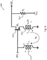
- Fig. 6 shows a half-circuit of a differential amplifier 600 using the principles of the circuit of Fig. 5 , but using a bifilar transformer 615 (indicated by dashed box) for T 1 .
- the primary winding 611, T 1,p is dc decoupled from secondary winding 612, T 1,s but still ac couples the negative feedback current from the source of transistor 610, M 1 to the gate thereof.
- Transformer T 2 is an autotransformer as before with primary winding 613, T 2,p and secondary winding 614, T 2,s .
- the ac ground nodes are indicated by nodes A and B at the bottom of the figure and the second half circuit is simply formed as a mirror image about these nodes.
- the transistor gates can be biased with a dc potential applied at node A.
- the low-noise amplifier can be biased with a dc current source connected to node B.
- node B can be connected to dc ground.
- the two primary windings T 1,p either side of node A form a centre-tapped inductor.
- the two secondary windings T 1,s either side of node B form a centre-tapped inductor.
- These two centre-tapped inductors can be formed as a single transformer, e.g., T 1 ' with centre-tapped primary and centre-tapped secondary windings.
- Figs. 7 to 10 show various simulation results of the circuit of Fig. 5 .
- Fig. 7 shows the forward transmission coefficient (S 21 ) of the low-noise amplifier of Fig. 5 .
- High gain greater than 15 dB is shown for frequencies above 6 GHz.
- Fig. 7 also shows that the low-noise amplifier has a single harmonic trap high-pass like frequency response with a notch around 3 GHz.
- Fig. 8 shows the input reflection coefficient (S 11 ) of the differential low-noise amplifier.
- Fig. 8 shows that the low-noise amplifier is impedance matched (S 11 ⁇ -10 dB) to 100 ⁇ over most of the passband (6 to 8.5 GHz).
- Fig. 9 shows the S 21 of the low-noise amplifier when combined with a passive high-pass filter (with and without active Q-boosting).
- the combined frequency response of the LNA with a high-pass filter results in > 50 dB rejection at round IEEE 802.11b/g (i.e., WLAN at 2.4 GHz).
- the high-pass filter used in this simulation includes a Q-boosting arrangement to boost the Q of the inductive components of the HPF. Results are shown in Fig. 9 with Q-boosting enabled as well as without Q-boosting enabled (i.e. with a fifth-order elliptic HPF).
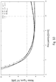
- Fig. 10 shows the noise figure of the the low-noise amplifier of Fig. 5 when combined with a passive high-pass filter (again, with and without active Q-boosting of the inductive components of the HPF).
- the differential LNA is biased at around the minimum possible noise figure. It is impedance (input only) and noise-matched to 100 ⁇ by proper sizing (i.e., aspect ratio, W/L) of the input common-source transistor M 1 in combination with the effective turns ratio realized by the negative reactive feedback loop comprising autotransformers T 1 and T 2 .
Landscapes
- Engineering & Computer Science (AREA)
- Power Engineering (AREA)
- Amplifiers (AREA)
Claims (15)
- Verstärker (500), umfassend:ein Verstärkungselement (510), das einen Eingang und einen Ausgang aufweist;einen ersten Transformator (T1); undeinen zweiten Transformator (T2);wobei der erste Transformator (T1) bei dem Ausgang des Verstärkungselements (510) eingerichtet ist, einen Teil des Ausgangsstroms von dem Verstärkungselement (510) über eine sekundäre Wicklung des ersten Transformators und eine sekundäre Wicklung des zweiten Transformators an einen Verstärkereingang (RFi,+) miteinander zu koppeln;wobei der zweite Transformator (T2) bei dem Eingang des Verstärkungselements eingerichtet ist, eine Spannung bei dem Eingang des Verstärkungselements (510) über gemeinsame Kopplung seiner primären (514) und sekundären (515) Wicklungen zu erhöhen;wobei die primäre Wicklung (512) des ersten Transformators (T1) mit dem Ausgang des Verstärkungselements (510) verbunden ist;wobei die sekundäre Wicklung (513) des ersten Transformators (T1) mit der sekundären Wicklung (515) des zweiten Transformators (T2) wechselstromverbunden ist, wobei die primäre Wicklung (T2,p) des zweiten Transformators (T2) zwischen dem Verstärkereingang (RFi,+) und dem Eingang des Verstärkungselements (510) verbunden ist; undwobei die primäre Wicklung (512) des ersten Transformators (T1) von der sekundären Wicklung (515) des zweiten Transformators (T2) gleichstromgesperrt ist.
- Verstärker (500) nach Anspruch 1, wobei der erste Transformator (T1) ein Autotransformator ist und wobei die sekundäre Wicklung (513) des ersten Transformators (T1) mit der sekundären Wicklung (515) des zweiten Transformators (T2) durch ein kapazitives Element (516) wechselstromverbunden ist, um die Gleichstromsperre bereitzustellen.
- Verstärker (500) nach Anspruch 2, wobei der erste Transformator (T1) ein symmetrischer Autotransformator ist.
- Verstärker (500) nach Anspruch 2, wobei die primäre Wicklung (512) und die sekundäre Wicklung (513) des ersten Transformators (T1) nicht gleichstromverbunden sind, sodass der erste Transformator (T1) die Gleichstromsperre bereitstellt.
- Verstärker (500) nach einem der vorstehenden Ansprüche, wobei der zweite Transformator (T2) ein Autotransformator ist.
- Verstärker (500) nach Anspruch 5, wobei der zweite Transformator (T2) ein symmetrischer Autotransformator ist.
- Verstärker (500) nach einem der vorstehenden Ansprüche, wobei der erste Transformator (T1) mit einem nichtinvertierenden Ausgang des Verstärkungselements (510) verbunden ist und wobei der erste Transformator (T1) als ein invertierender Transformator eingerichtet ist.
- Verstärker (500) nach einem der vorstehenden Ansprüche, wobei das Verstärkungselement (510) ein Transistor ist.
- Verstärker (500) nach einem der vorstehenden Ansprüche, wobei der zweite Transformator (T2) ein Autotransformator ist und wobei ein Signaleingang bei einer Zwischenabgriffsstelle des zweiten Transformators (T2) angelegt ist.
- Verstärker (500) nach einem der vorstehenden Ansprüche, wobei der erste Transformator (T1) ein Autotransformator ist und wobei eine Gleichstromquelle (518) mit einer Zwischenabgriffsstelle zwischen den primären (512) und sekundären (513) Wicklungen des ersten Transformators (T1) verbunden ist.
- Verstärker (500) nach einem der vorstehenden Ansprüche, wobei der erste Transformator (T1) ein Autotransformator ist, wobei der zweite Transformator (T2) ein Autotransformator ist und wobei die Eigeninduktivitäten der zweiten Transformatorwicklungen (514, 515) größer als die Eigeninduktivitäten der ersten Transformatorwicklungen (512, 513) sind.
- Differenzialverstärker (600), der eine positive Signalhälfte und eine negative Signalhälfte umfasst, wobei die positive Hälfte und die negative Hälfte jeweils einen Verstärker (500) nach einem der vorstehenden Ansprüche umfassen.
- Differenzialverstärker (600) nach Anspruch 12, wobei der erste Transformator (T1) sowohl in der positiven als auch negativen Hälfte eine primäre Wicklung (611) und eine sekundäre Wicklung (612) aufweist, die nicht gleichstromverbunden sind.
- Differenzialverstärker (600) nach Anspruch 13, wobei die primäre Wicklung (611) des ersten Transformators (T1) der positiven Hälfte und die primäre Wicklung (611) des ersten Transformators (T1) der negativen Hälfte direkt verbunden sind und eine primäre Wicklung eines mittenabgegriffenen Transformators bilden; und wobei die sekundäre Wicklung (612) des ersten Transformators (T1) der positiven Hälfte und die sekundäre Wicklung (612) des ersten Transformators (T1) der negativen Hälfte direkt verbunden sind und eine sekundäre Wicklung des mittenabgegriffenen Transformators bilden.
- Verfahren zum Verstärken eines Eingangssignals, umfassend:Erfassen eines Stroms bei einem Ausgang eines Verstärkungselements (510) mit einer primären Wicklung (512) eines Transformators (T1);Wechselstromkoppeln mindestens eines Teils des erfassten Stroms über eine sekundäre Wicklung (513)des ersten Transformators (T1) und eine sekundäre Wicklung (515) eines zweiten Transformators (T2) mit einem Eingang des Verstärkungselements (510); wobei die primäre Wicklung (512) des ersten Transformators (T1) von der sekundären Wicklung (515) des zweiten Transformators (T2) gleichstromgesperrt ist; undKoppeln eines Teils der Eingangssignalspannung über die sekundäre Wicklung (515) des zweiten Transformators (T2) und Hinzufügen davon zu einer Spannung bei dem Gate des Verstärkungselements (510) über die primäre Wicklung (514) des zweiten Transformators (T2).
Applications Claiming Priority (2)
| Application Number | Priority Date | Filing Date | Title |
|---|---|---|---|
| GBGB1614239.0A GB201614239D0 (en) | 2016-08-19 | 2016-08-19 | Amplifier |
| PCT/GB2017/052439 WO2018033743A1 (en) | 2016-08-19 | 2017-08-17 | Low noise amplifier with reactive feedback |
Publications (2)
| Publication Number | Publication Date |
|---|---|
| EP3501101A1 EP3501101A1 (de) | 2019-06-26 |
| EP3501101B1 true EP3501101B1 (de) | 2020-10-07 |
Family
ID=57045565
Family Applications (1)
| Application Number | Title | Priority Date | Filing Date |
|---|---|---|---|
| EP17757842.4A Active EP3501101B1 (de) | 2016-08-19 | 2017-08-17 | Rauscharmer verstärker mit reaktiver rückkopplung |
Country Status (6)
| Country | Link |
|---|---|
| US (1) | US10903805B2 (de) |
| EP (1) | EP3501101B1 (de) |
| CN (1) | CN109661774B (de) |
| GB (1) | GB201614239D0 (de) |
| TW (1) | TWI738846B (de) |
| WO (1) | WO2018033743A1 (de) |
Families Citing this family (10)
| Publication number | Priority date | Publication date | Assignee | Title |
|---|---|---|---|---|
| CN113451770A (zh) * | 2020-03-25 | 2021-09-28 | 深圳光启尖端技术有限责任公司 | 一种宽带匹配网络及天线 |
| CN111525894B (zh) * | 2020-06-08 | 2023-04-04 | 北京富奥星电子技术有限公司 | 一种宽带、高干扰消除能力的射频低噪声放大器 |
| CN112636705B (zh) * | 2020-12-10 | 2025-03-25 | 富满微电子集团股份有限公司 | 放大器电路及电子设备 |
| US11888453B2 (en) * | 2021-03-23 | 2024-01-30 | Qualcomm Incorporated | Wideband low-noise amplifier |
| US12176865B2 (en) * | 2021-10-14 | 2024-12-24 | Realtek Semiconductor Corp. | Integrated low-noise amplifier of compact layout |
| GB202118017D0 (en) | 2021-12-13 | 2022-01-26 | Novelda As | Receiver |
| GB202118014D0 (en) | 2021-12-13 | 2022-01-26 | Novelda As | Receiver |
| GB202118021D0 (en) | 2021-12-13 | 2022-01-26 | Novelda As | Receiver |
| CN121153195A (zh) * | 2023-03-27 | 2025-12-16 | 三星电子株式会社 | 无线通信系统中的低噪声放大器及使用其的接收机 |
| CN118074632B (zh) * | 2024-04-18 | 2024-07-09 | 浙江大学 | 低噪声放大器及无线通信系统 |
Citations (1)
| Publication number | Priority date | Publication date | Assignee | Title |
|---|---|---|---|---|
| WO2010007177A1 (en) * | 2008-07-17 | 2010-01-21 | Stichting Imec Nederland | Dual-loop feedback amplifying circuit |
Family Cites Families (4)
| Publication number | Priority date | Publication date | Assignee | Title |
|---|---|---|---|---|
| DE10325634B4 (de) * | 2003-06-06 | 2018-03-29 | Bruker Biospin Mri Gmbh | Rauscharmer Vorverstärker, insbesondere für die Kernspinresonanz(=NMR) |
| US8310309B2 (en) * | 2010-05-03 | 2012-11-13 | Qualcomm, Incorporated | Noise-canceling for differential amplifiers requiring no external matching |
| EP2466746B1 (de) * | 2010-12-16 | 2013-09-18 | TELEFONAKTIEBOLAGET LM ERICSSON (publ) | Rauscharmer Verstärker |
| US8912845B2 (en) * | 2013-01-07 | 2014-12-16 | Analog Devices, Inc. | Multiple winding transformer coupled amplifier |
-
2016
- 2016-08-19 GB GBGB1614239.0A patent/GB201614239D0/en not_active Ceased
-
2017
- 2017-08-16 TW TW106127731A patent/TWI738846B/zh active
- 2017-08-17 CN CN201780050890.9A patent/CN109661774B/zh active Active
- 2017-08-17 EP EP17757842.4A patent/EP3501101B1/de active Active
- 2017-08-17 US US16/326,469 patent/US10903805B2/en active Active
- 2017-08-17 WO PCT/GB2017/052439 patent/WO2018033743A1/en not_active Ceased
Patent Citations (1)
| Publication number | Priority date | Publication date | Assignee | Title |
|---|---|---|---|---|
| WO2010007177A1 (en) * | 2008-07-17 | 2010-01-21 | Stichting Imec Nederland | Dual-loop feedback amplifying circuit |
Also Published As
| Publication number | Publication date |
|---|---|
| US10903805B2 (en) | 2021-01-26 |
| WO2018033743A1 (en) | 2018-02-22 |
| GB201614239D0 (en) | 2016-10-05 |
| US20190356280A1 (en) | 2019-11-21 |
| TWI738846B (zh) | 2021-09-11 |
| CN109661774A (zh) | 2019-04-19 |
| CN109661774B (zh) | 2022-11-08 |
| EP3501101A1 (de) | 2019-06-26 |
| TW201822461A (zh) | 2018-06-16 |
Similar Documents
| Publication | Publication Date | Title |
|---|---|---|
| US10903805B2 (en) | Low noise amplifier with reactive feedback | |
| US7880547B2 (en) | Systems and methods for power amplifiers with voltage boosting multi-primary transformers | |
| CN101488729B (zh) | 功率放大器系统的多个段的初级和多匝的次级变压器 | |
| US11329613B2 (en) | Amplifier | |
| US8116700B2 (en) | Reducing common mode effects in an output stage | |
| JP2010056860A (ja) | 低雑音増幅器 | |
| KR102624600B1 (ko) | 스케일러블 rf 튜닝 저잡음 증폭기 | |
| US8988150B2 (en) | Amplifier and amplification method | |
| US20260019064A1 (en) | System and method for coupled resonator filtering | |
| US9966904B2 (en) | RF amplifier to increase gain using transformer | |
| CN111030621A (zh) | 一种用于无线终端的交流堆叠功率放大器 | |
| US20260058617A1 (en) | Low noise amplifier incorporating sutardja transformer | |
| CN110932687A (zh) | 一种交流堆叠功率放大器 | |
| US8264276B2 (en) | Low-noise amplifier | |
| CN118590020B (zh) | 一种多重电感耦合的低噪声放大器电路 | |
| EP4708677A1 (de) | Rauschunterdrückungsverstärker | |
| Khan et al. | Design & EM simulation of on-chip transformer baluns for RF power amplifiers | |
| CN109660215B (zh) | 一种宽频射频低噪声放大器的集成电路 |
Legal Events
| Date | Code | Title | Description |
|---|---|---|---|
| STAA | Information on the status of an ep patent application or granted ep patent |
Free format text: STATUS: UNKNOWN |
|
| STAA | Information on the status of an ep patent application or granted ep patent |
Free format text: STATUS: THE INTERNATIONAL PUBLICATION HAS BEEN MADE |
|
| PUAI | Public reference made under article 153(3) epc to a published international application that has entered the european phase |
Free format text: ORIGINAL CODE: 0009012 |
|
| STAA | Information on the status of an ep patent application or granted ep patent |
Free format text: STATUS: REQUEST FOR EXAMINATION WAS MADE |
|
| 17P | Request for examination filed |
Effective date: 20190319 |
|
| AK | Designated contracting states |
Kind code of ref document: A1 Designated state(s): AL AT BE BG CH CY CZ DE DK EE ES FI FR GB GR HR HU IE IS IT LI LT LU LV MC MK MT NL NO PL PT RO RS SE SI SK SM TR |
|
| AX | Request for extension of the european patent |
Extension state: BA ME |
|
| DAV | Request for validation of the european patent (deleted) | ||
| DAX | Request for extension of the european patent (deleted) | ||
| GRAP | Despatch of communication of intention to grant a patent |
Free format text: ORIGINAL CODE: EPIDOSNIGR1 |
|
| STAA | Information on the status of an ep patent application or granted ep patent |
Free format text: STATUS: GRANT OF PATENT IS INTENDED |
|
| INTG | Intention to grant announced |
Effective date: 20200302 |
|
| GRAS | Grant fee paid |
Free format text: ORIGINAL CODE: EPIDOSNIGR3 |
|
| GRAA | (expected) grant |
Free format text: ORIGINAL CODE: 0009210 |
|
| STAA | Information on the status of an ep patent application or granted ep patent |
Free format text: STATUS: THE PATENT HAS BEEN GRANTED |
|
| AK | Designated contracting states |
Kind code of ref document: B1 Designated state(s): AL AT BE BG CH CY CZ DE DK EE ES FI FR GB GR HR HU IE IS IT LI LT LU LV MC MK MT NL NO PL PT RO RS SE SI SK SM TR |
|
| REG | Reference to a national code |
Ref country code: GB Ref legal event code: FG4D |
|
| REG | Reference to a national code |
Ref country code: CH Ref legal event code: EP Ref country code: AT Ref legal event code: REF Ref document number: 1322253 Country of ref document: AT Kind code of ref document: T Effective date: 20201015 |
|
| REG | Reference to a national code |
Ref country code: DE Ref legal event code: R096 Ref document number: 602017025084 Country of ref document: DE |
|
| REG | Reference to a national code |
Ref country code: IE Ref legal event code: FG4D |
|
| REG | Reference to a national code |
Ref country code: NL Ref legal event code: MP Effective date: 20201007 |
|
| REG | Reference to a national code |
Ref country code: AT Ref legal event code: MK05 Ref document number: 1322253 Country of ref document: AT Kind code of ref document: T Effective date: 20201007 |
|
| PG25 | Lapsed in a contracting state [announced via postgrant information from national office to epo] |
Ref country code: GR Free format text: LAPSE BECAUSE OF FAILURE TO SUBMIT A TRANSLATION OF THE DESCRIPTION OR TO PAY THE FEE WITHIN THE PRESCRIBED TIME-LIMIT Effective date: 20210108 Ref country code: FI Free format text: LAPSE BECAUSE OF FAILURE TO SUBMIT A TRANSLATION OF THE DESCRIPTION OR TO PAY THE FEE WITHIN THE PRESCRIBED TIME-LIMIT Effective date: 20201007 Ref country code: NO Free format text: LAPSE BECAUSE OF FAILURE TO SUBMIT A TRANSLATION OF THE DESCRIPTION OR TO PAY THE FEE WITHIN THE PRESCRIBED TIME-LIMIT Effective date: 20210107 Ref country code: PT Free format text: LAPSE BECAUSE OF FAILURE TO SUBMIT A TRANSLATION OF THE DESCRIPTION OR TO PAY THE FEE WITHIN THE PRESCRIBED TIME-LIMIT Effective date: 20210208 Ref country code: RS Free format text: LAPSE BECAUSE OF FAILURE TO SUBMIT A TRANSLATION OF THE DESCRIPTION OR TO PAY THE FEE WITHIN THE PRESCRIBED TIME-LIMIT Effective date: 20201007 |
|
| REG | Reference to a national code |
Ref country code: LT Ref legal event code: MG4D |
|
| PG25 | Lapsed in a contracting state [announced via postgrant information from national office to epo] |
Ref country code: SE Free format text: LAPSE BECAUSE OF FAILURE TO SUBMIT A TRANSLATION OF THE DESCRIPTION OR TO PAY THE FEE WITHIN THE PRESCRIBED TIME-LIMIT Effective date: 20201007 Ref country code: PL Free format text: LAPSE BECAUSE OF FAILURE TO SUBMIT A TRANSLATION OF THE DESCRIPTION OR TO PAY THE FEE WITHIN THE PRESCRIBED TIME-LIMIT Effective date: 20201007 Ref country code: IS Free format text: LAPSE BECAUSE OF FAILURE TO SUBMIT A TRANSLATION OF THE DESCRIPTION OR TO PAY THE FEE WITHIN THE PRESCRIBED TIME-LIMIT Effective date: 20210207 Ref country code: LV Free format text: LAPSE BECAUSE OF FAILURE TO SUBMIT A TRANSLATION OF THE DESCRIPTION OR TO PAY THE FEE WITHIN THE PRESCRIBED TIME-LIMIT Effective date: 20201007 Ref country code: BG Free format text: LAPSE BECAUSE OF FAILURE TO SUBMIT A TRANSLATION OF THE DESCRIPTION OR TO PAY THE FEE WITHIN THE PRESCRIBED TIME-LIMIT Effective date: 20210107 Ref country code: ES Free format text: LAPSE BECAUSE OF FAILURE TO SUBMIT A TRANSLATION OF THE DESCRIPTION OR TO PAY THE FEE WITHIN THE PRESCRIBED TIME-LIMIT Effective date: 20201007 Ref country code: AT Free format text: LAPSE BECAUSE OF FAILURE TO SUBMIT A TRANSLATION OF THE DESCRIPTION OR TO PAY THE FEE WITHIN THE PRESCRIBED TIME-LIMIT Effective date: 20201007 |
|
| PG25 | Lapsed in a contracting state [announced via postgrant information from national office to epo] |
Ref country code: NL Free format text: LAPSE BECAUSE OF FAILURE TO SUBMIT A TRANSLATION OF THE DESCRIPTION OR TO PAY THE FEE WITHIN THE PRESCRIBED TIME-LIMIT Effective date: 20201007 Ref country code: HR Free format text: LAPSE BECAUSE OF FAILURE TO SUBMIT A TRANSLATION OF THE DESCRIPTION OR TO PAY THE FEE WITHIN THE PRESCRIBED TIME-LIMIT Effective date: 20201007 |
|
| REG | Reference to a national code |
Ref country code: DE Ref legal event code: R097 Ref document number: 602017025084 Country of ref document: DE |
|
| PG25 | Lapsed in a contracting state [announced via postgrant information from national office to epo] |
Ref country code: RO Free format text: LAPSE BECAUSE OF FAILURE TO SUBMIT A TRANSLATION OF THE DESCRIPTION OR TO PAY THE FEE WITHIN THE PRESCRIBED TIME-LIMIT Effective date: 20201007 Ref country code: SK Free format text: LAPSE BECAUSE OF FAILURE TO SUBMIT A TRANSLATION OF THE DESCRIPTION OR TO PAY THE FEE WITHIN THE PRESCRIBED TIME-LIMIT Effective date: 20201007 Ref country code: CZ Free format text: LAPSE BECAUSE OF FAILURE TO SUBMIT A TRANSLATION OF THE DESCRIPTION OR TO PAY THE FEE WITHIN THE PRESCRIBED TIME-LIMIT Effective date: 20201007 Ref country code: EE Free format text: LAPSE BECAUSE OF FAILURE TO SUBMIT A TRANSLATION OF THE DESCRIPTION OR TO PAY THE FEE WITHIN THE PRESCRIBED TIME-LIMIT Effective date: 20201007 Ref country code: LT Free format text: LAPSE BECAUSE OF FAILURE TO SUBMIT A TRANSLATION OF THE DESCRIPTION OR TO PAY THE FEE WITHIN THE PRESCRIBED TIME-LIMIT Effective date: 20201007 Ref country code: SM Free format text: LAPSE BECAUSE OF FAILURE TO SUBMIT A TRANSLATION OF THE DESCRIPTION OR TO PAY THE FEE WITHIN THE PRESCRIBED TIME-LIMIT Effective date: 20201007 |
|
| PLBE | No opposition filed within time limit |
Free format text: ORIGINAL CODE: 0009261 |
|
| STAA | Information on the status of an ep patent application or granted ep patent |
Free format text: STATUS: NO OPPOSITION FILED WITHIN TIME LIMIT |
|
| PG25 | Lapsed in a contracting state [announced via postgrant information from national office to epo] |
Ref country code: DK Free format text: LAPSE BECAUSE OF FAILURE TO SUBMIT A TRANSLATION OF THE DESCRIPTION OR TO PAY THE FEE WITHIN THE PRESCRIBED TIME-LIMIT Effective date: 20201007 |
|
| 26N | No opposition filed |
Effective date: 20210708 |
|
| PG25 | Lapsed in a contracting state [announced via postgrant information from national office to epo] |
Ref country code: AL Free format text: LAPSE BECAUSE OF FAILURE TO SUBMIT A TRANSLATION OF THE DESCRIPTION OR TO PAY THE FEE WITHIN THE PRESCRIBED TIME-LIMIT Effective date: 20201007 Ref country code: IT Free format text: LAPSE BECAUSE OF FAILURE TO SUBMIT A TRANSLATION OF THE DESCRIPTION OR TO PAY THE FEE WITHIN THE PRESCRIBED TIME-LIMIT Effective date: 20201007 |
|
| PG25 | Lapsed in a contracting state [announced via postgrant information from national office to epo] |
Ref country code: SI Free format text: LAPSE BECAUSE OF FAILURE TO SUBMIT A TRANSLATION OF THE DESCRIPTION OR TO PAY THE FEE WITHIN THE PRESCRIBED TIME-LIMIT Effective date: 20201007 |
|
| REG | Reference to a national code |
Ref country code: CH Ref legal event code: PL |
|
| PG25 | Lapsed in a contracting state [announced via postgrant information from national office to epo] |
Ref country code: MC Free format text: LAPSE BECAUSE OF FAILURE TO SUBMIT A TRANSLATION OF THE DESCRIPTION OR TO PAY THE FEE WITHIN THE PRESCRIBED TIME-LIMIT Effective date: 20201007 |
|
| REG | Reference to a national code |
Ref country code: BE Ref legal event code: MM Effective date: 20210831 |
|
| PG25 | Lapsed in a contracting state [announced via postgrant information from national office to epo] |
Ref country code: LI Free format text: LAPSE BECAUSE OF NON-PAYMENT OF DUE FEES Effective date: 20210831 Ref country code: CH Free format text: LAPSE BECAUSE OF NON-PAYMENT OF DUE FEES Effective date: 20210831 |
|
| PG25 | Lapsed in a contracting state [announced via postgrant information from national office to epo] |
Ref country code: IS Free format text: LAPSE BECAUSE OF FAILURE TO SUBMIT A TRANSLATION OF THE DESCRIPTION OR TO PAY THE FEE WITHIN THE PRESCRIBED TIME-LIMIT Effective date: 20210207 Ref country code: LU Free format text: LAPSE BECAUSE OF NON-PAYMENT OF DUE FEES Effective date: 20210817 |
|
| PG25 | Lapsed in a contracting state [announced via postgrant information from national office to epo] |
Ref country code: IE Free format text: LAPSE BECAUSE OF NON-PAYMENT OF DUE FEES Effective date: 20210817 Ref country code: BE Free format text: LAPSE BECAUSE OF NON-PAYMENT OF DUE FEES Effective date: 20210831 |
|
| P01 | Opt-out of the competence of the unified patent court (upc) registered |
Effective date: 20230513 |
|
| PG25 | Lapsed in a contracting state [announced via postgrant information from national office to epo] |
Ref country code: CY Free format text: LAPSE BECAUSE OF FAILURE TO SUBMIT A TRANSLATION OF THE DESCRIPTION OR TO PAY THE FEE WITHIN THE PRESCRIBED TIME-LIMIT Effective date: 20201007 |
|
| PG25 | Lapsed in a contracting state [announced via postgrant information from national office to epo] |
Ref country code: HU Free format text: LAPSE BECAUSE OF FAILURE TO SUBMIT A TRANSLATION OF THE DESCRIPTION OR TO PAY THE FEE WITHIN THE PRESCRIBED TIME-LIMIT; INVALID AB INITIO Effective date: 20170817 |
|
| PG25 | Lapsed in a contracting state [announced via postgrant information from national office to epo] |
Ref country code: MK Free format text: LAPSE BECAUSE OF FAILURE TO SUBMIT A TRANSLATION OF THE DESCRIPTION OR TO PAY THE FEE WITHIN THE PRESCRIBED TIME-LIMIT Effective date: 20201007 |
|
| PG25 | Lapsed in a contracting state [announced via postgrant information from national office to epo] |
Ref country code: TR Free format text: LAPSE BECAUSE OF FAILURE TO SUBMIT A TRANSLATION OF THE DESCRIPTION OR TO PAY THE FEE WITHIN THE PRESCRIBED TIME-LIMIT Effective date: 20201007 |
|
| PG25 | Lapsed in a contracting state [announced via postgrant information from national office to epo] |
Ref country code: MT Free format text: LAPSE BECAUSE OF FAILURE TO SUBMIT A TRANSLATION OF THE DESCRIPTION OR TO PAY THE FEE WITHIN THE PRESCRIBED TIME-LIMIT Effective date: 20201007 |
|
| PGFP | Annual fee paid to national office [announced via postgrant information from national office to epo] |
Ref country code: DE Payment date: 20250917 Year of fee payment: 9 |
|
| PGFP | Annual fee paid to national office [announced via postgrant information from national office to epo] |
Ref country code: GB Payment date: 20250916 Year of fee payment: 9 |
|
| PGFP | Annual fee paid to national office [announced via postgrant information from national office to epo] |
Ref country code: FR Payment date: 20250917 Year of fee payment: 9 |