EP3506655B1 - Instrument auditif comprenant une antenne à induction magnétique - Google Patents
Instrument auditif comprenant une antenne à induction magnétique Download PDFInfo
- Publication number
- EP3506655B1 EP3506655B1 EP17211040.5A EP17211040A EP3506655B1 EP 3506655 B1 EP3506655 B1 EP 3506655B1 EP 17211040 A EP17211040 A EP 17211040A EP 3506655 B1 EP3506655 B1 EP 3506655B1
- Authority
- EP
- European Patent Office
- Prior art keywords
- pulses
- sequence
- phase
- antenna resonator
- hearing instrument
- Prior art date
- Legal status (The legal status is an assumption and is not a legal conclusion. Google has not performed a legal analysis and makes no representation as to the accuracy of the status listed.)
- Active
Links
Images




Classifications
-
- H—ELECTRICITY
- H04—ELECTRIC COMMUNICATION TECHNIQUE
- H04R—LOUDSPEAKERS, MICROPHONES, GRAMOPHONE PICK-UPS OR LIKE ACOUSTIC ELECTROMECHANICAL TRANSDUCERS; ELECTRIC HEARING AIDS; PUBLIC ADDRESS SYSTEMS
- H04R25/00—Electric hearing aids
- H04R25/55—Electric hearing aids using an external connection, either wireless or wired
- H04R25/554—Electric hearing aids using an external connection, either wireless or wired using a wireless connection, e.g. between microphone and amplifier or using Tcoils
-
- H—ELECTRICITY
- H04—ELECTRIC COMMUNICATION TECHNIQUE
- H04R—LOUDSPEAKERS, MICROPHONES, GRAMOPHONE PICK-UPS OR LIKE ACOUSTIC ELECTROMECHANICAL TRANSDUCERS; ELECTRIC HEARING AIDS; PUBLIC ADDRESS SYSTEMS
- H04R25/00—Electric hearing aids
- H04R25/50—Customised settings for obtaining desired overall acoustical characteristics
-
- H—ELECTRICITY
- H04—ELECTRIC COMMUNICATION TECHNIQUE
- H04R—LOUDSPEAKERS, MICROPHONES, GRAMOPHONE PICK-UPS OR LIKE ACOUSTIC ELECTROMECHANICAL TRANSDUCERS; ELECTRIC HEARING AIDS; PUBLIC ADDRESS SYSTEMS
- H04R25/00—Electric hearing aids
- H04R25/50—Customised settings for obtaining desired overall acoustical characteristics
- H04R25/505—Customised settings for obtaining desired overall acoustical characteristics using digital signal processing
-
- H—ELECTRICITY
- H04—ELECTRIC COMMUNICATION TECHNIQUE
- H04R—LOUDSPEAKERS, MICROPHONES, GRAMOPHONE PICK-UPS OR LIKE ACOUSTIC ELECTROMECHANICAL TRANSDUCERS; ELECTRIC HEARING AIDS; PUBLIC ADDRESS SYSTEMS
- H04R25/00—Electric hearing aids
- H04R25/55—Electric hearing aids using an external connection, either wireless or wired
- H04R25/558—Remote control, e.g. of amplification, frequency
-
- H—ELECTRICITY
- H04—ELECTRIC COMMUNICATION TECHNIQUE
- H04R—LOUDSPEAKERS, MICROPHONES, GRAMOPHONE PICK-UPS OR LIKE ACOUSTIC ELECTROMECHANICAL TRANSDUCERS; ELECTRIC HEARING AIDS; PUBLIC ADDRESS SYSTEMS
- H04R2225/00—Details of deaf aids covered by H04R25/00, not provided for in any of its subgroups
- H04R2225/43—Signal processing in hearing aids to enhance the speech intelligibility
-
- H—ELECTRICITY
- H04—ELECTRIC COMMUNICATION TECHNIQUE
- H04R—LOUDSPEAKERS, MICROPHONES, GRAMOPHONE PICK-UPS OR LIKE ACOUSTIC ELECTROMECHANICAL TRANSDUCERS; ELECTRIC HEARING AIDS; PUBLIC ADDRESS SYSTEMS
- H04R2225/00—Details of deaf aids covered by H04R25/00, not provided for in any of its subgroups
- H04R2225/51—Aspects of antennas or their circuitry in or for hearing aids
-
- H—ELECTRICITY
- H04—ELECTRIC COMMUNICATION TECHNIQUE
- H04R—LOUDSPEAKERS, MICROPHONES, GRAMOPHONE PICK-UPS OR LIKE ACOUSTIC ELECTROMECHANICAL TRANSDUCERS; ELECTRIC HEARING AIDS; PUBLIC ADDRESS SYSTEMS
- H04R2225/00—Details of deaf aids covered by H04R25/00, not provided for in any of its subgroups
- H04R2225/55—Communication between hearing aids and external devices via a network for data exchange
Definitions
- the present disclosure relates to hearing instruments, such as hearing instruments for compensating a hearing loss of a user, such hearing instruments providing audio to a user, and particularly to hearing instruments having wireless communication capabilities, such as hearing instruments including an magnetic induction antenna, and particular to hearing instruments comprising magnetic induction antennas for communication, and particularly for hearing instruments efficiently driving a magnetic induction antenna.
- Hearing instruments of any kind have over the later years been increasingly able to communicate with the surroundings, including communicating with remote controls, spouse microphones, other hearing instruments and nowadays also directly with smart phones and other external electronic devices.
- Hearing instruments are very small and delicate devices and to fulfil the above requirements, the hearing instruments need to comprise many electronic and metallic components contained in a housing small enough to fit in the ear canal of a human or behind the outer ear.
- the many electronic and metallic components in combination with the small size of the hearing instrument housing impose high design constraints on any antennas to be used in hearing instruments with wireless communication capabilities.
- Radio frequency antennas have been used in hearing instruments to achieve connectivity with a wide range of devices.
- magnetic induction antennas are being used in hearing instruments.
- Hearing instruments are supplied with power from hearing instrument batteries, having a limited power supply, and for the users, longer lifetime or longer time-between-charging for such hearing instrument batteries is expected, even when the capabilities of the hearing instruments are improved.
- the hearing instrument comprises a number of electronic components, which are all supplied with power from the battery. Thus, optimization of power usage is a concern for all electronic components in the hearing instrument, and particular wireless communication may consume significant power. Therefore, for antennas in hearing instruments in general, there is a need to ensure that the antennas and the communication protocols are designed to reduce the power consumption while maintaining a high efficiency.
- magnetic induction antennas may be preferred due to e.g. increased efficiency, minimized absorption by the head, etc.
- EP 1 777 644 A1 shows a system and method for driving an antenna.
- the system comprises a driving means driving the antenna with a driving signal.
- the system further comprises a modulation means having an input receiving a transmission data signal, a data identification means identifying a level change in the transmission data signal and controlling duty cycle of the driving signal.
- the data identification means provides a timed increase of duty cycle of the driving signal when the a level change in said transmission data is identified.
- WO 95/01678 A1 shows a short range magnetically coupled wireless communication system that employs time variant modulation of a high repetition rate pulse stream and magnetic coupling between a transmission magnetic element and a receiving magnetic element.
- the pulse stream is modulated by an input audio frequency signal in the time domain, for example through pulse position modulation, pulse width modulation or pulse symmetry modulation.
- the receiving magnetic element is coupled to a demodulator circuit which detects the transmitted pulses induced in the receiving magnetic element and reproduces the audio frequency signal. Transmission over short range is thus efficiently accomplished through magnetic coupling in a simple low cost low power consumption communication system.
- the present invention is disclosed by the subject-matter of the independent claims.
- One aspect of the present invention is a hearing instrument as defined in independent claim 1.
- Another aspect of the invention is a method as defined in independent claim 12. Further aspects of the invention are the subject of the dependent claims.
- the antenna resonator is driven efficiently, such that the antenna resonator has a low power consumption during use. It is an advantage that by supplying power to the antenna resonator for excitation of the antenna resonator using a first sequence of pulses, such as using a first and a second sequence of pulses, the second sequence of pulses having a frequency which is phase shifted with respect to the phase of the first sequence of pulses, power consumption of the antenna resonator may be reduced.
- the signal processor is connected to the driving circuit and configured to provide a signal, such as a data signal, such as a data communication signal, such as a digital data signal, to the driving circuit.
- the driving circuit is configured for digital modulation of the signal received from the signal processor.
- the digital modulation may be any digital modulation, such as digital modulation based on keying and may output a modulated signal.
- the digital modulation is a frequency modulation, such as frequency-shift keying.
- the digital modulation is an amplitude modulation, such as amplitude-shift keying.
- the digital modulation is a phase modulation, such as phase-shift keying.
- the data may thus be conveyed by modulating the phase of a carrier wave or reference signal.
- the phase-shift keying, PSK may be any type of phase-shift keying, including binary phase-shift keying, BPSK, quadrature phase-shift keying, QPSK, differential phase-shift keying, DPSK, higher order phase-shift keying, and/or any combinations or derivatives of these modulation methods.
- the driving circuit may comprise any components as known by a skilled person to implement the digital modulation, including one or more of clock generators, pulse generators and/or modulators.
- the driving circuit further comprises a splitter and/or a phase shifter to split and phase shift the modulated signal to thereby obtain a driving circuit output comprising a first sequence of pulses having a first phase and a first pulse width, and a second sequence of pulses having a second phase and a second pulse width, wherein the second phase is being phase shifted with respect to the first phase.
- a splitter and/or phase shifter are optional elements, and that a driving circuit output having a single sequence of pulses having a first phase and a first pulse width may be provided to the oscillator circuitry to supply power to the antenna resonator for excitation of the antenna resonator.
- the first pulse width and the second pulse width of the driving circuit output are determined with respect to the first frequency.
- the first pulse width and/or the second pulse width may be 1/4 of the first frequency, such as 1/6 of the first frequency, such as 1/8 of the first frequency.
- the first pulse width and/or the second pulse width is according to the invention less than 1/4 of the first frequency.
- the first pulse width and/or the second pulse width may be between 1/4 of the first frequency and 1/100 of the first frequency, such as between 1/4 of the first frequency and 1/10 of the first frequency, such as between 1/4 of the first frequency and 1/8 of the first frequency, such as approximately 1/6 of the first frequency.
- the relation or correspondence of pulse width to frequency is given by 1/f.
- the first sequence of pulses has a first period and the second sequence of pulses has a second period, the first period and the second period being determined as a fraction of the inverse of the first frequency.
- the first period and the second period may be the inverse of the first frequency, such as 1/f 1 , where f 1 is the first frequency.
- the first period and the second period may be between 1/f 1 and one hundredth of 1/f 1 , such as between one fourth of 1/f 1 and one hundredth of 1/f 1 , such as between one tenth of 1/f 1 and one hundredth of 1/f 1 , between one fourth of 1/f 1 and one tenth of 1/f 1 , such as between one sixth of 1/f 1 and one tenth of 1/f 1 , such as about one sixth of 1/f 1 .
- the first period and the second period may be a same period.
- the energy density of the driving circuit output is determined at least partly by the first pulse width and the second pulse width and/or the energy density of the driving circuit output is determined at least partly by the amplitude of the first sequence of pulses and the amplitude of the second sequence of pulses, or any combination thereof.
- increasing the pulse width or increasing the amplitude of the first pulses and the second pulses, respectively increases the energy density of the driving circuit output.
- decreasing the pulse width or decreasing the amplitude of the first and second pulses, respectively decreases the energy density of the driving circuit output.
- any changes of the pulse width, such as of the pulse width magnitude, and/or of the pulse amplitude, such as of a pulse amplitude magnitude will change the energy density of the driving circuit output.
- the pulses in the first sequence of pulses have a first constant amplitude
- the pulses of the second sequence of pulses have a second constant amplitude.
- the first constant amplitude may correspond to the second constant amplitude, such that the first constant amplitude and the second constant amplitude may have the same constant amplitude, such as the same constant amplitude having a same magnitude.
- the antenna resonator being configured to inductively transmit and receive an electromagnetic field is a magnetic induction antenna.
- the antenna resonator comprises a resonant circuit.
- the antenna resonator may comprise an inductor and a capacitor, the inductor and the capacitor forming an oscillating circuit, such as a resonant circuit.
- the antenna resonator is configured to be driven by the driving circuit output.
- the antenna resonator has a resonant frequency, i.e. corresponding to the first frequency, being determined by the inductive reactance magnitude and the capacitive reactance magnitude of the antenna resonator. Tuning of the inductive reactance magnitude and the capacitive reactance magnitude of antenna resonator may thus tune the resonance frequency and thereby the first frequency. Likewise, changes to the resonance frequency may be implemented by tuning the inductive reactance magnitude and the capacitive reactance magnitude of the antenna resonator.
- the antenna resonator comprises an inductor and a capacitor provided in parallel. In some embodiments, the antenna resonator comprises an inductor and a capacitor provided in series. The configuration providing the optimum properties for a specific use may be selected.
- the antenna resonator will not be a loss-less antenna resonator, rather a loss resulting from small but non-zero resistance within the components and connecting wires will be present.
- the presence of resistance in the oscillating circuit will dampen the oscillations of the oscillating circuit.
- the driving circuit is configured to overcome the loss to ensure continuous oscillation at the resonance frequency.
- the antenna resonator will be designed having a high Q-factor, and thus low loss, to minimize the power or energy density required to ensure continuous oscillation.
- the first frequency, and thus the resonance frequency of the antenna resonator is between 1 MHz and 20 MHz, such as between 6 MHz and 14 MHz, such as about 6.7 MHz, such as about 13.6 MHz.
- the resonance frequency may be selected as a resonance frequency of an ISM band.
- the inductive transmission is a short-range communication and the range of the transmitted electromagnetic field is typically below 1 meter.
- the antenna resonator has a first input terminal and a second input terminal.
- the first input terminal may be provided at a first connection between the capacitor and the inductor
- the second input terminal may be provided at the second connection, parallel to the first connection, between the capacitor and the inductor.
- the first input terminal may be an input to the inductor and the second input terminal may be an input to the capacitor, or vice versa.
- the driving circuit output is provided to the first input terminal and to the second input terminal via the signal control switches.
- the driving circuit output is provided to the first input terminal or to the second input terminal via the signal control switches, while the other of the first and second input terminals is connected to ground.
- the sequential pulses including the first sequence of pulses and the second sequence of pulses, have an energy density or power corresponding to the loss present in the antenna resonator, or in the oscillator circuitry.
- the energy density of the driving circuit output may be configured to counter the loss present in the antenna resonator or in the oscillator circuitry.
- the energy density of the driving circuit output may be configured to ensure continuous oscillation of the antenna resonator.
- the energy density of the driving circuit output may be configured to balance, such as to off-set, a loss in the antenna resonator and/or in the oscillator circuitry.
- the energy density of the driving circuit output may be of a same or similar magnitude as the loss in the antenna resonator or the oscillator circuitry.
- the energy density of the driving circuit output may be of a same or similar magnitude, such as 10% higher than the loss in the antenna resonator or the oscillator circuitry.
- maximum antenna resonator voltage may be controlled by controlling pulse width and/or amplitude of the first sequence of pulses and the second sequence of pulses.
- the antenna resonator may be driven with an ability to adjust maximum resonator voltage and the amount of energy pumped into the resonator.
- a corresponding antenna resonator receiver may be provided within the near-field, such as within the magnetic near-field, of the antenna resonator transmitting an electromagnetic field, i.e. within the near-field of an antenna resonator transmitter for receiving the transmitted electromagnetic field.
- a first hearing instrument comprising an antenna resonator as herein described may be provided at a first ear of a user and may communicate via the antenna resonator with a second hearing instrument, such as a second hearing instrument provided at a second ear of a user, comprising a corresponding antenna resonator for receiving the transmitted electromagnetic field.
- the clock generator as provided in the wireless communication unit at the first ear of a user may be synchronized with a clock generator as provided in a wireless communication unit at the second ear.
- the hearing instrument may be any hearing instrument, including hearing instruments compensating a hearing loss of a user, hearing instruments providing audio to a user, including headsets, earphones, etc.
- the hearing instrument may be any hearing instruments having wireless communication capabilities.
- the hearing instrument may be a hearing instrument compensating a hearing loss of a user, and the hearing instrument may be any type of hearing instrument, including in-the-ear hearing instruments, completely-in-the-canal hearing instruments, behind-the-ear hearing instruments, receiver-in-the ear hearing instruments, and any combination of such hearing instruments or hearing aids compensating a hearing loss of a user.
- the hearing instrument may furthermore be a headset, such as a headset or set of earphones having on-the-ear earphones, particularly such as a headset or earphones being configured to be arranged in or at the ear of a user.
- the wireless communication unit may be configured to communicate with another hearing instrument, such as another hearing instrument provided at another ear of a user; the wireless communication unit may be configured to communicate with accessory devices for the hearing instruments, such as including remote controls, spouse microphones, etc.; the wireless communication unit may be configured to communicate with other wearable electronic devices, such as including smart watches, etc. and any combination of these.
- a hearing instrument such as a hearing aid.
- the hearing aid may be a binaural hearing aid. It is however envisaged that any embodiments or elements as described in connection with any one aspect may be used with any other aspects or embodiments, mutatis mutandis.
- FIG. 1 A block-diagram of a typical (prior-art) hearing instrument 2 is shown in Fig. 1 .
- the hearing instrument 2 comprises a first transducer, i.e. microphone 3, for receiving incoming sound and converting it into an audio signal, i.e. a first audio signal.
- the first audio signal is provided to a signal processor 5.
- the signal processor is configured for processing the first audio signal into a second audio signal compensating a hearing loss of a user of the hearing instrument.
- a receiver or speaker 8 is connected to an output of the signal processor 5 for converting the second audio signal into an output sound signal, such as for example a signal modified to compensate for a user's hearing impairment, such as for example a noise reduced signal, etc., and provides the output sound to the speaker 8.
- the receiver 8 comprises a transducer, and the receiver 8 may be referred to as speaker 8.
- the hearing instrument signal processor 5 comprises elements such as amplifiers, compressors and noise reduction systems etc.
- the hearing instrument or hearing aid may further have a filter function 7, such as compensation filter for optimizing the output signal.
- the hearing instrument furthermore has a wireless communication unit 4 for wireless data communication configured for emission and reception of an electromagnetic field.
- the wireless communication unit 4 connect to the hearing instrument signal processor 5, for communicating with external devices, such as with another hearing instrument, such as with another hearing instrument located at another ear, such as for example in a binaural hearing instrument system.
- the hearing instrument 2 further comprises a power source 6, such as a battery 6.
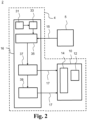
- Fig. 2 shows schematically a hearing instrument 2 comprising a wireless communication unit 4 and a signal processor 5.
- the wireless communication unit 4 is connected to the signal processor 5 for wireless communication.
- the wireless communication unit 4 is configured to inductively transmit and receive an electromagnetic field.
- the wireless communication unit comprises an oscillator circuitry 10 comprising an antenna resonator 12 and signal control switches 14.
- the antenna resonator is configured to emit an electromagnetic field at a first frequency.
- the wireless communication unit 4 further comprises a driving circuit 16 for driving the oscillator circuitry 10.
- the driving circuit 16 provides a driving circuit output 17 comprising a first sequence of pulses 18 (see Fig. 7 ), the first sequence of pulses 18 having a first phase and a first pulse width 25 (see Fig.
- the driving circuit output 17, including the first sequence of pulses 18 and the second sequence of pulses 19, is provided to the oscillator circuitry 10 to supply power to the antenna resonator 12 for excitation of the antenna resonator.
- the driving circuit 16 comprises clock generator 31, pulse generator 33 and modulator 35 to modulate the incoming data signal.
- the modulator output comprises a sequence of pulses and is provided to splitter 37 to provide a first output and a second output, wherein the first output of the splitter 37 is provided as first driving circuit output 17 comprising a first sequence of pulses 18, and the second output of splitter 37 is provided to phase shifter 39 configured to shift the phase of the second output.
- the phase shifted second output of splitter 37 is provided as second driving circuit output 17 comprising a second sequence of pulses 19.
- the driving circuit output 17 comprises a signal representing data and carrier frequency.
- Fig. 3 shows schematically a hearing instrument 2 comprising a wireless communication unit 4 and a signal processor 5. Same reference numerals refer to same features as in Fig. 2 .
- a modulating unit 34 is provided comprising the clock generator 31, pulse generator 33 and modulator 35 configured to modulate the data signal 15.
- the splitter 37 and the phase shifter 39 is provided separately from the modulating unit. It is envisaged that the components of the modulating unit 34 may be provided as an integrated circuit, such as provided as part of an IC chip.
- the splitter 37 and the phase shifter 39 may, as seen in Fig. 2 , be provided with the modulating unit 34, such as at a same IC chip. However, it is envisaged, as seen in Fig.
- the splitter 37 and phase shifter 39 may be provided separately from e.g. an IC chip comprising the modulating unit 34.
- the modulating unit 34, the splitter 37 and the phase shifter 39 may be provided at a same printed circuit board in the hearing instrument.
- the oscillating circuit 10 and the signal processor 5 may be provided on the same printed circuit board.
- the modulating unit 34, the splitter 37 and the phase shifter 39, and possibly also the oscillating circuit 10 and signal processor 5 may be provided at a number of different printed circuit boards in the hearing instrument or in the wireless communication unit 4.
- the splitter 37 and the phase shifter 39 may be dispensed with so that a single driving circuit output 17 is provided comprising a first sequence of pulses 18.
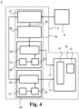
- Fig. 4 shows schematically a hearing instrument 2 comprising a wireless communication unit 4 and a signal processor 5. Same reference numerals refer to same features as in Fig. 2 .
- a splitter 37 receives the signal from the signal processor 5, and splits the signal into a first signal 36 and a second signal 38.
- the first signal 36 is provided to a first modulating unit 34 comprising clock generator 31, pulse generator 33 and modulator 35 for modulating of the first signal 36
- the second signal 38 is provided to phase shifter 39 for phase shifting of the second signal 38.
- the phase shifted second signal is provided to second modulating unit 34' comprising clock generator 31, pulse generator 33 and modulator 35 for modulating of the phase shifted second signal.
- the output 17 of the first modulating unit 34 and the output 17' of the second modulating unit 34' are provided as driving circuit output 17, 17' to the oscillating circuit 10.
- splitter 37 and phase shifter 39 may be implemented using any methods and components as will be known to a skilled person. Thus, the splitter 37 and phase shifter 39 will not be described in further detail.
- Figs. 5a and 5b show schematically oscillating circuits 10 comprising signal control switches 14 and antenna resonators 12.
- the oscillating circuit 10 comprises antenna resonator 12 and signal control switches 14.
- the antenna resonator 12 comprises an inductor 41 and a capacitor 42.
- the antenna resonator comprising at least an inductor and a capacitor may be implemented in any known way, including using a number of components to obtain a preferred antenna resonator.
- the antenna resonator is implemented with a parallel coupled inductor and capacitor.
- the antenna resonator has a first input terminal 45 and a second input terminal 46.
- the first input terminal 45 is provided at a first side of the antenna resonator 12, and the second input terminal 46 is provided at a second side of the antenna resonator 12.
- the switching control switches 14 are supplied with power at supply 48.
- the power is supplied from a power source 6 of the wireless communication unit, such as from a power source 6 of the hearing instrument, such as from a battery 6.
- the switching control switches are connected to ground 40, such as to a ground potential of a printed circuit board (not shown).
- the switching control switches comprise first, second, third and fourth control switches 51, 52, 53, 54. It is seen that at the first side of the antenna resonator 12, there is a potential difference over first control switch 51 and second control switch 52. Likewise, on the second side of the antenna resonator 12, there is a potential difference over the third control switch 53 and the fourth control switch 54.
- the driving circuit output is provided to the switching control switches.
- a first driving circuit output 17 comprising the first sequence of pulses18 is provided to first control switch 51 and to third control switch 53.
- a second driving circuit output 17' comprising the second sequence of pulses19 is provided to second control switch 52 and to the fourth control switch 54.
- the control switches 51, 52, 53 and 54 are configured to close when a pulse is received, that is the control switches are normally open switches and closes when a pulse is received.
- the first and third control switches 51, 53 will close thereby creating a potential difference over the antenna resonator and supply power to the antenna resonator.
- the second and fourth control switches 52, 54 will close thereby creating a potential difference having opposite sign with respect to the potential difference created at the receipt of a pulse of the first sequence of pulses and supply power with opposite sign to the antenna resonator.
- an alternating voltage will be supplied to the antenna resonator to thereby excite the antenna resonator.
- the oscillating circuit comprises antenna resonator 12 and signal control switches 14.
- the antenna resonator 12 is seen to comprise an inductor 41 and a capacitor 42. In the present embodiment, it is seen that the antenna resonator is implemented with inductor and capacitor coupled in series.
- the antenna resonator has a first input terminal 45 and a second input terminal 46. The first input terminal 45 is provided at a first side of the antenna resonator 12, and the second input terminal 46 is provided at a second side of the antenna resonator 12.
- the further implementation is as set out above for Fig. 5a .
- Figs. 6a and 6b further oscillating circuits 10 according to the present disclosure is shown. Same reference numerals refer to same features as in Figs. 5a and 5b .
- the oscillating circuit 10 comprises antenna resonator 12 and signal control switches 14.
- the antenna resonator 12 is seen to comprise an inductor 41 and a capacitor 42. In the present embodiment, it is seen that the antenna resonator is implemented as parallel coupled inductor 41 and capacitor 42.
- the antenna resonator has a first input terminal 45 and a second input terminal 46.
- the first input terminal 45 is provided at a first side of the antenna resonator 12, and the second input terminal 46 is provided at a second side of the antenna resonator 12.
- the driving circuit output is provided to the switching control switches.
- a first driving circuit output 17 comprising the first sequence of pulses 18 is provided to first control switch 51.
- a second driving circuit output 17' comprising the second sequence of pulses19 is provided to second control switch 52.
- First and second control switches 51, 52 are connected to the first input terminal 45 of the antenna resonator 12.
- the second input terminal 46 of the antenna resonator 12 is connected to ground 40.
- the control switch 51 will when closed connect the first input terminal 45 to power supply potential 48.
- the control switch 52 will when closed connect the first input terminal 45 to negative supply power 49.
- the control switches 51, 52 are configured to close when a pulse is received, that is the control switches are normally open switches and closes when a pulse is received.
- the first control switch 51 When a pulse of the first sequence of pulses is received at the first control switch 51, the first control switch 51 will close thereby creating a potential difference over the antenna resonator and supply power to the antenna resonator. Likewise, when a pulse of the second sequence of pulses is received at the second control switches 52, the second control switch 52 will close thereby creating a potential difference having opposite sign with respect to the potential difference created at the receipt of a pulse of the first sequence of pulses and supply power with opposite sign to the antenna resonator. Thus, upon receiving the first and second sequence of pulses 18, 19, an alternating voltage will be supplied to the antenna resonator to thereby exite, or ensure excitation, of the antenna resonator.
- the oscillating circuit 10 comprises antenna resonator 12 and signal control switch 14.
- the antenna resonator 12 is seen to comprise an inductor 41 and a capacitor 42.
- the antenna resonator is implemented as parallel coupled inductor 41 and capacitor 42.
- the antenna resonator has a first input terminal 45 and a second input terminal 46.
- the first input terminal 45 is provided at a first side of the antenna resonator 12, and the second input terminal 46 is provided at a second side of the antenna resonator 12.
- the driving circuit output is provided to the switching control switch 14 comprising control switch 51.
- the driving circuit output 17 comprising a sequence of pulses 18 is provided to the control switch 51.
- the control switch 51 is connected to the first input terminal 45 of the antenna resonator 12.
- the second input terminal 46 of the antenna resonator 12 is connected to ground 40.
- the control switch 51 will when closed connect the first input terminal 45 to power supply potential 48.
- the control switch 51 will when open connect the first input terminal 45 to negative supply power 49 or to ground 40 (not shown).
- the control switch 51 is configured to close when a pulse is received, that is the control switch is a normally open switch and closes when a pulse is received.
- the first control switch 51 When a pulse of the first sequence of pulses is received at the first control switch 51, the first control switch 51 will close thereby creating a potential difference over the antenna resonator and supply power to the antenna resonator. Thus, upon receiving the sequence of pulses 18, a voltage will be supplied to the antenna resonator to thereby exite, or ensure excitation, of the antenna resonator using short pulse excitation.
- Fig. 7 illustrates a driving circuit output comprising a first sequence of pulses 18 and a second sequence of pulses 19.
- the pulses in the second sequence of pulses 19 are phase shifted 180 degrees with respect to the pulses in the first sequence of pulses 18.
- the distance between a first flange of a pulse in the first sequence of pulses and a first flange of a pulse in the second sequence of pulses is 1 ⁇ 2 t.
- the amplitude 23 of the pulses is given by the height of the pulses.
- the pulse width 25 of the pulses is given by the width of the pulses.
- the pulse width 25 of the pulses in the first and second sequence of pulses 18, 19 is constant and the pulse width of the pulses in the first sequence of pulses corresponds to the pulse width of the pulses in the second sequence of pulses.
- the amplitude 23 of the pulses 20 in the first and second sequence of pulses 18, 19 is constant and the amplitude 23 of the pulses 20 in the first sequence of pulses 18 corresponds to, such as is equal to, such as is substantially equal to, the amplitude 23 of the pulses 20 in the second sequence of pulses 19.
- the pulse width and the amplitude may vary and still be considered constant and corresponding within the meaning of the present disclosure, for example if the variation is less than 10%.
- the amplitude of the pulses in the first and second sequence of pulses may control whether the switches 51, 52, 53, 54 switches (i.e. closes or opens) upon receipt of the pulse.
- the amplitude 23 of the pulses 20 in the first and second sequence of pulses is configured to be above a threshold amplitude value, to ensure switching of the switch from open to close or vice versa.
- the hearing instrument may be a behind-the ear hearing instrument, and may be provided as a behind-the-ear module, the hearing instrument may be an in-the-ear module and may be provided as an in-the-ear module.
- parts of the hearing instrument may be provided in a behind-the-ear module, while other parts, such as the receiver, may be provided in an in-the-ear module.
Landscapes
- Engineering & Computer Science (AREA)
- Computer Networks & Wireless Communication (AREA)
- Health & Medical Sciences (AREA)
- General Health & Medical Sciences (AREA)
- Neurosurgery (AREA)
- Otolaryngology (AREA)
- Physics & Mathematics (AREA)
- Acoustics & Sound (AREA)
- Signal Processing (AREA)
- Transmitters (AREA)
- Near-Field Transmission Systems (AREA)
Claims (12)
- Appareil auditif comprenantun microphone pour la réception du son et la conversion du son reçu en un premier signal audio correspondant,un processeur de signal pour traiter le premier signal audio en un deuxième signal audio compensant une perte auditive d'un utilisateur de l'aide auditive, un haut-parleur connecté à une sortie du processeur de signal pour convertir le deuxième signal audio en un signal sonore de sortie,une unité de communication sans fil connectée au processeur de signal pour une communication sans fil, l'unité de communication sans fil étant configurée pour transmettre et recevoir de manière inductive un champ électromagnétique,l'unité de communication sans fil comprenantun circuit d'oscillateur comprenant un résonateur d'antenne et des commutateurs de commande de signal, le résonateur d'antenne étant configuré pour émettre un champ électromagnétique à une première fréquence,un circuit pilote pour les circuit d'oscillateur,dans lequel le circuit pilote fournit une sortie de circuit de pilote comprenant- une première séquence d'impulsions, la première séquence d'impulsions ayant une première phase et une première largeur d'impulsion, la première largeur d'impulsion étant inférieure à 1/4 d'un inverse de la première fréquence, et- une deuxième séquence d'impulsions, la deuxième séquence d'impulsions ayant une deuxième phase et une deuxième largeur d'impulsion, la deuxième largeur d'impulsion étant inférieure à 1/4 d'un inverse de la première fréquence, la deuxième phase étant déphasée par rapport à la première phase, la première phase et la deuxième phase étant déterminées en fonction de la première fréquence,dans lequel la première séquence d'impulsions et la deuxième séquence d'impulsions sont fournies à au moins un premier commutateur de commande de signal et un deuxième commutateur de commande de signal, et dans lequel au moins les premier et deuxième commutateurs de commande de signal sont configurés de telle sorte que, lors de la réception de la première séquence d'impulsions et la seconde séquence d'impulsions, une tension alternative sera fournie au résonateur d'antenne pour exciter ainsi le résonateur d'antenne.
- Appareil auditif selon la revendication 1, dans lequel la deuxième phase est déphasée de 180° par rapport à la première phase.
- Appareil auditif selon l'une quelconque des revendications précédentes, dans lequel l'antenne résonatrice est une antenne à induction magnétique.
- Appareil auditif selon l'une quelconque des revendications précédentes, dans lequel la première séquence d'impulsions a une première période et la deuxième séquence d'impulsions a une deuxième période, la première période et la deuxième période étant déterminées comme une fraction de l'inverse de la première fréquence.
- Appareil auditif selon la revendication 4, caractérisé en ce que la fraction est comprise entre le centième et le quart.
- Appareil auditif selon l'une quelconque des revendications précédentes, dans lequel une densité d'énergie de la sortie du circuit de pilote est déterminée au moins en partie par la première largeur d'impulsion et la deuxième largeur d'impulsion, et/ou au moins en partie par l'amplitude de la première séquence d'impulsions et l'amplitude de la deuxième séquence d'impulsions.
- Appareil auditif selon l'une quelconque des revendications précédentes, dans lequel les impulsions de la première séquence d'impulsions ont une première amplitude constante, et dans lequel les impulsions de la deuxième séquence d'impulsions ont une deuxième amplitude constante.
- Appareil auditif selon la revendication 7, dans lequel la première amplitude constante et la deuxième amplitude constante sont la même amplitude constante.
- Appareil auditif selon l'une quelconque des revendications précédentes, dans lequel le résonateur d'antenne comprend une inductance et un condensateur fournis en parallèle, ou dans lequel le résonateur d'antenne comprend une inductance et un condensateur fournis en série.
- Appareil auditif selon l'un quelconque des revendications précédents, dans lequel la première fréquence est comprise entre 1 MHz et 20 MHz.
- Appareil auditif selon l'une quelconque des revendications précédentes, dans lequel le résonateur d'antenne a une première borne d'entrée et une seconde borne d'entrée, et dans lequel la sortie du circuit de pilote est fournie à la première borne d'entrée et à la seconde borne d'entrée via les commutateurs de commande de signal.
- Procédé de fonctionnement d'un appareil auditif, l'appareil auditif comprenant un microphone pour la réception du son et la conversion du son reçu en un premier signal audio correspondant, un processeur de signal pour traiter le premier signal audio en un deuxième signal audio compensant une audition perte d'un utilisateur de l'aide auditive, un haut-parleur connecté à une sortie du processeur de signal pour convertir le deuxième signal audio en un signal sonore de sortie, une unité de communication sans fil connectée au processeur de signal pour une communication sans fil, l'unité de communication sans fil étant configurée transmettre et recevoir de manière inductive un champ électromagnétique,l'unité de communication sans fil comprenant un circuit oscillateur comprenantun résonateur d'antenne et des commutateurs de commande de signal, le résonateur d'antenne étant configuré pour transmettre un champ électromagnétique à une première fréquence, et un circuit de pilote pour les circuit d'oscillateur, le procédé comprenant la génération par le circuit de pilote d'une sortie de circuit de pilote comprenant- une première séquence d'impulsions, la première séquence d'impulsions ayant une première phase et une première largeur d'impulsion, la première largeur d'impulsion étant inférieure à 1/4 d'un inverse de la première fréquence, et- une deuxième séquence d'impulsions, la deuxième séquence d'impulsions ayant une deuxième phase et une deuxième largeur d'impulsion, la deuxième largeur d'impulsion étant inférieure à 1/4 d'un inverse de la première fréquence, la deuxième phase étant déphasée par rapport à la première phase, la première phase et la deuxième phase étant déterminées en fonction de la première fréquence,fournir la sortie du circuit de pilote à au moins un premier commutateur de commande de signal et un deuxième commutateur de commande de signal configurés pour recevoir la première séquence d'impulsions et la deuxième séquence d'impulsions,lors de la réception de la première séquence d'impulsions et de la deuxième séquence d'impulsions, les premier et deuxième commutateurs de commande de signal fournissent une tension alternative au résonateur d'antenne pour exciter ainsi le résonateur d'antenne.
Priority Applications (4)
| Application Number | Priority Date | Filing Date | Title |
|---|---|---|---|
| EP17211040.5A EP3506655B1 (fr) | 2017-12-29 | 2017-12-29 | Instrument auditif comprenant une antenne à induction magnétique |
| US16/185,942 US10715935B2 (en) | 2017-12-29 | 2018-11-09 | Hearing instrument comprising a magnetic induction antenna |
| JP2018233804A JP2019146151A (ja) | 2017-12-29 | 2018-12-13 | 磁気誘導アンテナを有する聴覚機器 |
| CN201811579963.6A CN109996163B (zh) | 2017-12-29 | 2018-12-24 | 包括磁感应天线的听力仪器 |
Applications Claiming Priority (1)
| Application Number | Priority Date | Filing Date | Title |
|---|---|---|---|
| EP17211040.5A EP3506655B1 (fr) | 2017-12-29 | 2017-12-29 | Instrument auditif comprenant une antenne à induction magnétique |
Publications (3)
| Publication Number | Publication Date |
|---|---|
| EP3506655A1 EP3506655A1 (fr) | 2019-07-03 |
| EP3506655C0 EP3506655C0 (fr) | 2024-08-14 |
| EP3506655B1 true EP3506655B1 (fr) | 2024-08-14 |
Family
ID=60856936
Family Applications (1)
| Application Number | Title | Priority Date | Filing Date |
|---|---|---|---|
| EP17211040.5A Active EP3506655B1 (fr) | 2017-12-29 | 2017-12-29 | Instrument auditif comprenant une antenne à induction magnétique |
Country Status (4)
| Country | Link |
|---|---|
| US (1) | US10715935B2 (fr) |
| EP (1) | EP3506655B1 (fr) |
| JP (1) | JP2019146151A (fr) |
| CN (1) | CN109996163B (fr) |
Families Citing this family (6)
| Publication number | Priority date | Publication date | Assignee | Title |
|---|---|---|---|---|
| DE102018212957B3 (de) | 2018-08-02 | 2020-01-02 | Fraunhofer-Gesellschaft zur Förderung der angewandten Forschung e.V. | Übertragung von daten von einem benutzerendgerät zu einem anderen gerät |
| DE102018214716A1 (de) | 2018-08-30 | 2020-03-05 | Fraunhofer-Gesellschaft zur Förderung der angewandten Forschung e.V. | Übertragung von daten zwischen einem benutzerendgerät und einem anderen gerät |
| DE102019201152B3 (de) * | 2019-01-30 | 2020-06-18 | Fraunhofer-Gesellschaft zur Förderung der angewandten Forschung e.V. | Bidirektionale Konfiguration von Sensorknoten mit Mobiltelefon ohne Erweiterung |
| DE102019206836A1 (de) | 2019-05-10 | 2020-11-12 | Fraunhofer-Gesellschaft zur Förderung der angewandten Forschung e.V. | Effiziente Kommunikation zur Konfiguration von Sensorknoten |
| WO2021167715A1 (fr) | 2020-02-21 | 2021-08-26 | Qualcomm Incorporated | Traitement de signal de référence de positionnement |
| KR20220159373A (ko) * | 2020-03-26 | 2022-12-02 | 퀄컴 인코포레이티드 | 적어도 하나의 psi(positioning state information) 보고 엘리먼트의 연기된 보고를 위한 방법들 및 장치들 |
Family Cites Families (8)
| Publication number | Priority date | Publication date | Assignee | Title |
|---|---|---|---|---|
| US5615229A (en) * | 1993-07-02 | 1997-03-25 | Phonic Ear, Incorporated | Short range inductively coupled communication system employing time variant modulation |
| US6639990B1 (en) * | 1998-12-03 | 2003-10-28 | Arthur W. Astrin | Low power full duplex wireless link |
| US7512448B2 (en) * | 2003-01-10 | 2009-03-31 | Phonak Ag | Electrode placement for wireless intrabody communication between components of a hearing system |
| EP1777644B1 (fr) * | 2005-10-20 | 2009-01-21 | Oticon A/S | Système et procédé d'actionnement d'antenne |
| EP2223487B1 (fr) * | 2007-11-12 | 2011-08-03 | Widex A/S | Récepteur fsk pour une prothèse auditive et procédé de traitement d'un signal fsk |
| US9432780B2 (en) * | 2010-07-03 | 2016-08-30 | Starkey Laboratories, Inc. | Multi-mode radio for hearing assistance devices |
| US9319808B2 (en) * | 2012-11-19 | 2016-04-19 | Gn Resound A/S | Hearing aid having a near field resonant parasitic element |
| CN104735601B (zh) * | 2015-02-10 | 2019-03-26 | 惠州Tcl移动通信有限公司 | 一种助听线圈检测装置及检测系统 |
-
2017
- 2017-12-29 EP EP17211040.5A patent/EP3506655B1/fr active Active
-
2018
- 2018-11-09 US US16/185,942 patent/US10715935B2/en active Active
- 2018-12-13 JP JP2018233804A patent/JP2019146151A/ja active Pending
- 2018-12-24 CN CN201811579963.6A patent/CN109996163B/zh active Active
Also Published As
| Publication number | Publication date |
|---|---|
| JP2019146151A (ja) | 2019-08-29 |
| CN109996163B (zh) | 2022-08-23 |
| EP3506655A1 (fr) | 2019-07-03 |
| US20190208336A1 (en) | 2019-07-04 |
| CN109996163A (zh) | 2019-07-09 |
| EP3506655C0 (fr) | 2024-08-14 |
| US10715935B2 (en) | 2020-07-14 |
Similar Documents
| Publication | Publication Date | Title |
|---|---|---|
| EP3506655B1 (fr) | Instrument auditif comprenant une antenne à induction magnétique | |
| US11375321B2 (en) | Eartip venting in a contact hearing system | |
| JP5891387B2 (ja) | 無線電力データ伝送システム、送電装置、および受電装置 | |
| DK2476266T3 (en) | Hearing Aid with wireless battery charging capacity | |
| US8275462B1 (en) | Integrated phase-shift power control transmitter for use with implantable device and method for use of the same | |
| CA2825413A1 (fr) | Systeme de prothese auditive et prothese auditive | |
| DK1692778T3 (da) | Annullering af resonansfrekvensskift i trådløse høreapparater | |
| US20090029646A1 (en) | Communications device, a system and method using inductive communication | |
| US8483417B2 (en) | Configuration and method for wireless data transmission between hearing devices | |
| US6639990B1 (en) | Low power full duplex wireless link | |
| JP2019146150A (ja) | 無給電バッテリアンテナ素子を備えた聴覚器具 | |
| US7239713B2 (en) | Wireless transmission system for hearing devices | |
| US11689864B2 (en) | Hearing device and method of operating the hearing device | |
| WO2016003437A1 (fr) | Circuits émetteurs de radiofréquences alimentant en énergie un dispositif d'implant | |
| AU2012238219B2 (en) | RF Transmitter for Electrically Short Antenna | |
| AU2006202994B2 (en) | Hearing device without reference clock component | |
| EP2056626B1 (fr) | Principe de transmission sans fil | |
| WO2011010106A1 (fr) | Système de communications | |
| EP2721840B1 (fr) | Appareil auditif avec émetteur-récepteur sans fil et procédé d'adaptation | |
| EP4057639A1 (fr) | Dispositif auditif comprenant un module | |
| US7737799B2 (en) | Digital phase modulator and corresponding method | |
| WO2009001233A1 (fr) | Émetteur à puissance efficace pour liaison magnétique | |
| KR200220461Y1 (ko) | 900MHz 대역 무선 전화기의 전압 제어 발진 회로 | |
| CN119908126A (zh) | 听力设备以及用于运行听力设备的方法 | |
| WO2016187721A1 (fr) | Dispositif d'aide auditive |
Legal Events
| Date | Code | Title | Description |
|---|---|---|---|
| PUAI | Public reference made under article 153(3) epc to a published international application that has entered the european phase |
Free format text: ORIGINAL CODE: 0009012 |
|
| STAA | Information on the status of an ep patent application or granted ep patent |
Free format text: STATUS: THE APPLICATION HAS BEEN PUBLISHED |
|
| AK | Designated contracting states |
Kind code of ref document: A1 Designated state(s): AL AT BE BG CH CY CZ DE DK EE ES FI FR GB GR HR HU IE IS IT LI LT LU LV MC MK MT NL NO PL PT RO RS SE SI SK SM TR |
|
| AX | Request for extension of the european patent |
Extension state: BA ME |
|
| STAA | Information on the status of an ep patent application or granted ep patent |
Free format text: STATUS: REQUEST FOR EXAMINATION WAS MADE |
|
| 17P | Request for examination filed |
Effective date: 20191220 |
|
| RBV | Designated contracting states (corrected) |
Designated state(s): AL AT BE BG CH CY CZ DE DK EE ES FI FR GB GR HR HU IE IS IT LI LT LU LV MC MK MT NL NO PL PT RO RS SE SI SK SM TR |
|
| STAA | Information on the status of an ep patent application or granted ep patent |
Free format text: STATUS: EXAMINATION IS IN PROGRESS |
|
| 17Q | First examination report despatched |
Effective date: 20200211 |
|
| INTG | Intention to grant announced |
Effective date: 20220713 |
|
| GRAJ | Information related to disapproval of communication of intention to grant by the applicant or resumption of examination proceedings by the epo deleted |
Free format text: ORIGINAL CODE: EPIDOSDIGR1 |
|
| INTC | Intention to grant announced (deleted) | ||
| GRAP | Despatch of communication of intention to grant a patent |
Free format text: ORIGINAL CODE: EPIDOSNIGR1 |
|
| STAA | Information on the status of an ep patent application or granted ep patent |
Free format text: STATUS: GRANT OF PATENT IS INTENDED |
|
| INTG | Intention to grant announced |
Effective date: 20240313 |
|
| GRAS | Grant fee paid |
Free format text: ORIGINAL CODE: EPIDOSNIGR3 |
|
| GRAA | (expected) grant |
Free format text: ORIGINAL CODE: 0009210 |
|
| STAA | Information on the status of an ep patent application or granted ep patent |
Free format text: STATUS: THE PATENT HAS BEEN GRANTED |
|
| AK | Designated contracting states |
Kind code of ref document: B1 Designated state(s): AL AT BE BG CH CY CZ DE DK EE ES FI FR GB GR HR HU IE IS IT LI LT LU LV MC MK MT NL NO PL PT RO RS SE SI SK SM TR |
|
| REG | Reference to a national code |
Ref country code: GB Ref legal event code: FG4D |
|
| REG | Reference to a national code |
Ref country code: CH Ref legal event code: EP |
|
| REG | Reference to a national code |
Ref country code: DE Ref legal event code: R096 Ref document number: 602017084037 Country of ref document: DE |
|
| REG | Reference to a national code |
Ref country code: IE Ref legal event code: FG4D |
|
| U01 | Request for unitary effect filed |
Effective date: 20240819 |
|
| U07 | Unitary effect registered |
Designated state(s): AT BE BG DE DK EE FI FR IT LT LU LV MT NL PT SE SI Effective date: 20240828 |
|
| PG25 | Lapsed in a contracting state [announced via postgrant information from national office to epo] |
Ref country code: NO Free format text: LAPSE BECAUSE OF FAILURE TO SUBMIT A TRANSLATION OF THE DESCRIPTION OR TO PAY THE FEE WITHIN THE PRESCRIBED TIME-LIMIT Effective date: 20241114 |
|
| PG25 | Lapsed in a contracting state [announced via postgrant information from national office to epo] |
Ref country code: GR Free format text: LAPSE BECAUSE OF FAILURE TO SUBMIT A TRANSLATION OF THE DESCRIPTION OR TO PAY THE FEE WITHIN THE PRESCRIBED TIME-LIMIT Effective date: 20241115 Ref country code: PL Free format text: LAPSE BECAUSE OF FAILURE TO SUBMIT A TRANSLATION OF THE DESCRIPTION OR TO PAY THE FEE WITHIN THE PRESCRIBED TIME-LIMIT Effective date: 20240814 |
|
| U20 | Renewal fee for the european patent with unitary effect paid |
Year of fee payment: 8 Effective date: 20241217 |
|
| PG25 | Lapsed in a contracting state [announced via postgrant information from national office to epo] |
Ref country code: IS Free format text: LAPSE BECAUSE OF FAILURE TO SUBMIT A TRANSLATION OF THE DESCRIPTION OR TO PAY THE FEE WITHIN THE PRESCRIBED TIME-LIMIT Effective date: 20241214 |
|
| PG25 | Lapsed in a contracting state [announced via postgrant information from national office to epo] |
Ref country code: HR Free format text: LAPSE BECAUSE OF FAILURE TO SUBMIT A TRANSLATION OF THE DESCRIPTION OR TO PAY THE FEE WITHIN THE PRESCRIBED TIME-LIMIT Effective date: 20240814 |
|
| PG25 | Lapsed in a contracting state [announced via postgrant information from national office to epo] |
Ref country code: RS Free format text: LAPSE BECAUSE OF FAILURE TO SUBMIT A TRANSLATION OF THE DESCRIPTION OR TO PAY THE FEE WITHIN THE PRESCRIBED TIME-LIMIT Effective date: 20241114 Ref country code: ES Free format text: LAPSE BECAUSE OF FAILURE TO SUBMIT A TRANSLATION OF THE DESCRIPTION OR TO PAY THE FEE WITHIN THE PRESCRIBED TIME-LIMIT Effective date: 20240814 |
|
| PG25 | Lapsed in a contracting state [announced via postgrant information from national office to epo] |
Ref country code: RS Free format text: LAPSE BECAUSE OF FAILURE TO SUBMIT A TRANSLATION OF THE DESCRIPTION OR TO PAY THE FEE WITHIN THE PRESCRIBED TIME-LIMIT Effective date: 20241114 Ref country code: PL Free format text: LAPSE BECAUSE OF FAILURE TO SUBMIT A TRANSLATION OF THE DESCRIPTION OR TO PAY THE FEE WITHIN THE PRESCRIBED TIME-LIMIT Effective date: 20240814 Ref country code: NO Free format text: LAPSE BECAUSE OF FAILURE TO SUBMIT A TRANSLATION OF THE DESCRIPTION OR TO PAY THE FEE WITHIN THE PRESCRIBED TIME-LIMIT Effective date: 20241114 Ref country code: IS Free format text: LAPSE BECAUSE OF FAILURE TO SUBMIT A TRANSLATION OF THE DESCRIPTION OR TO PAY THE FEE WITHIN THE PRESCRIBED TIME-LIMIT Effective date: 20241214 Ref country code: HR Free format text: LAPSE BECAUSE OF FAILURE TO SUBMIT A TRANSLATION OF THE DESCRIPTION OR TO PAY THE FEE WITHIN THE PRESCRIBED TIME-LIMIT Effective date: 20240814 Ref country code: GR Free format text: LAPSE BECAUSE OF FAILURE TO SUBMIT A TRANSLATION OF THE DESCRIPTION OR TO PAY THE FEE WITHIN THE PRESCRIBED TIME-LIMIT Effective date: 20241115 Ref country code: ES Free format text: LAPSE BECAUSE OF FAILURE TO SUBMIT A TRANSLATION OF THE DESCRIPTION OR TO PAY THE FEE WITHIN THE PRESCRIBED TIME-LIMIT Effective date: 20240814 |
|
| PG25 | Lapsed in a contracting state [announced via postgrant information from national office to epo] |
Ref country code: SM Free format text: LAPSE BECAUSE OF FAILURE TO SUBMIT A TRANSLATION OF THE DESCRIPTION OR TO PAY THE FEE WITHIN THE PRESCRIBED TIME-LIMIT Effective date: 20240814 |
|
| PGFP | Annual fee paid to national office [announced via postgrant information from national office to epo] |
Ref country code: CH Payment date: 20250101 Year of fee payment: 8 |
|
| PG25 | Lapsed in a contracting state [announced via postgrant information from national office to epo] |
Ref country code: CZ Free format text: LAPSE BECAUSE OF FAILURE TO SUBMIT A TRANSLATION OF THE DESCRIPTION OR TO PAY THE FEE WITHIN THE PRESCRIBED TIME-LIMIT Effective date: 20240814 |
|
| PG25 | Lapsed in a contracting state [announced via postgrant information from national office to epo] |
Ref country code: SK Free format text: LAPSE BECAUSE OF FAILURE TO SUBMIT A TRANSLATION OF THE DESCRIPTION OR TO PAY THE FEE WITHIN THE PRESCRIBED TIME-LIMIT Effective date: 20240814 |
|
| PLBE | No opposition filed within time limit |
Free format text: ORIGINAL CODE: 0009261 |
|
| STAA | Information on the status of an ep patent application or granted ep patent |
Free format text: STATUS: NO OPPOSITION FILED WITHIN TIME LIMIT |
|
| PG25 | Lapsed in a contracting state [announced via postgrant information from national office to epo] |
Ref country code: MC Free format text: LAPSE BECAUSE OF FAILURE TO SUBMIT A TRANSLATION OF THE DESCRIPTION OR TO PAY THE FEE WITHIN THE PRESCRIBED TIME-LIMIT Effective date: 20240814 |
|
| 26N | No opposition filed |
Effective date: 20250515 |
|
| PG25 | Lapsed in a contracting state [announced via postgrant information from national office to epo] |
Ref country code: IE Free format text: LAPSE BECAUSE OF NON-PAYMENT OF DUE FEES Effective date: 20241229 |
|
| PG25 | Lapsed in a contracting state [announced via postgrant information from national office to epo] |
Ref country code: RO Free format text: LAPSE BECAUSE OF FAILURE TO SUBMIT A TRANSLATION OF THE DESCRIPTION OR TO PAY THE FEE WITHIN THE PRESCRIBED TIME-LIMIT Effective date: 20240814 |
|
| REG | Reference to a national code |
Ref country code: CH Ref legal event code: U11 Free format text: ST27 STATUS EVENT CODE: U-0-0-U10-U11 (AS PROVIDED BY THE NATIONAL OFFICE) Effective date: 20260101 |
|
| PGFP | Annual fee paid to national office [announced via postgrant information from national office to epo] |
Ref country code: GB Payment date: 20251219 Year of fee payment: 9 |
|
| U20 | Renewal fee for the european patent with unitary effect paid |
Year of fee payment: 9 Effective date: 20251216 |