EP3513241B1 - Microscope à champ lumineux à éclairage sélectif dans un plan - Google Patents
Microscope à champ lumineux à éclairage sélectif dans un plan Download PDFInfo
- Publication number
- EP3513241B1 EP3513241B1 EP17781545.3A EP17781545A EP3513241B1 EP 3513241 B1 EP3513241 B1 EP 3513241B1 EP 17781545 A EP17781545 A EP 17781545A EP 3513241 B1 EP3513241 B1 EP 3513241B1
- Authority
- EP
- European Patent Office
- Prior art keywords
- light
- sample
- illumination
- detection
- plane
- Prior art date
- Legal status (The legal status is an assumption and is not a legal conclusion. Google has not performed a legal analysis and makes no representation as to the accuracy of the status listed.)
- Active
Links
Images




Classifications
-
- G—PHYSICS
- G02—OPTICS
- G02B—OPTICAL ELEMENTS, SYSTEMS OR APPARATUS
- G02B21/00—Microscopes
- G02B21/06—Means for illuminating specimens
- G02B21/08—Condensers
- G02B21/082—Condensers for incident illumination only
-
- G—PHYSICS
- G01—MEASURING; TESTING
- G01N—INVESTIGATING OR ANALYSING MATERIALS BY DETERMINING THEIR CHEMICAL OR PHYSICAL PROPERTIES
- G01N21/00—Investigating or analysing materials by the use of optical means, i.e. using sub-millimetre waves, infrared, visible or ultraviolet light
- G01N21/62—Systems in which the material investigated is excited whereby it emits light or causes a change in wavelength of the incident light
- G01N21/63—Systems in which the material investigated is excited whereby it emits light or causes a change in wavelength of the incident light optically excited
- G01N21/64—Fluorescence; Phosphorescence
- G01N21/645—Specially adapted constructive features of fluorimeters
- G01N21/6456—Spatial resolved fluorescence measurements; Imaging
- G01N21/6458—Fluorescence microscopy
-
- G—PHYSICS
- G02—OPTICS
- G02B—OPTICAL ELEMENTS, SYSTEMS OR APPARATUS
- G02B21/00—Microscopes
- G02B21/0004—Microscopes specially adapted for specific applications
- G02B21/002—Scanning microscopes
- G02B21/0024—Confocal scanning microscopes (CSOMs) or confocal "macroscopes"; Accessories which are not restricted to use with CSOMs, e.g. sample holders
- G02B21/0032—Optical details of illumination, e.g. light-sources, pinholes, beam splitters, slits, fibers
-
- G—PHYSICS
- G02—OPTICS
- G02B—OPTICAL ELEMENTS, SYSTEMS OR APPARATUS
- G02B21/00—Microscopes
- G02B21/0004—Microscopes specially adapted for specific applications
- G02B21/002—Scanning microscopes
- G02B21/0024—Confocal scanning microscopes (CSOMs) or confocal "macroscopes"; Accessories which are not restricted to use with CSOMs, e.g. sample holders
- G02B21/008—Details of detection or image processing, including general computer control
-
- G—PHYSICS
- G02—OPTICS
- G02B—OPTICAL ELEMENTS, SYSTEMS OR APPARATUS
- G02B21/00—Microscopes
- G02B21/16—Microscopes adapted for ultraviolet illumination ; Fluorescence microscopes
-
- G—PHYSICS
- G02—OPTICS
- G02B—OPTICAL ELEMENTS, SYSTEMS OR APPARATUS
- G02B21/00—Microscopes
- G02B21/24—Base structure
- G02B21/26—Stages; Adjusting means therefor
-
- G—PHYSICS
- G02—OPTICS
- G02B—OPTICAL ELEMENTS, SYSTEMS OR APPARATUS
- G02B21/00—Microscopes
- G02B21/36—Microscopes arranged for photographic purposes or projection purposes or digital imaging or video purposes including associated control and data processing arrangements
- G02B21/361—Optical details, e.g. image relay to the camera or image sensor
-
- G—PHYSICS
- G02—OPTICS
- G02B—OPTICAL ELEMENTS, SYSTEMS OR APPARATUS
- G02B21/00—Microscopes
- G02B21/36—Microscopes arranged for photographic purposes or projection purposes or digital imaging or video purposes including associated control and data processing arrangements
- G02B21/365—Control or image processing arrangements for digital or video microscopes
-
- G—PHYSICS
- G02—OPTICS
- G02B—OPTICAL ELEMENTS, SYSTEMS OR APPARATUS
- G02B21/00—Microscopes
- G02B21/36—Microscopes arranged for photographic purposes or projection purposes or digital imaging or video purposes including associated control and data processing arrangements
- G02B21/365—Control or image processing arrangements for digital or video microscopes
- G02B21/367—Control or image processing arrangements for digital or video microscopes providing an output produced by processing a plurality of individual source images, e.g. image tiling, montage, composite images, depth sectioning, image comparison
-
- G—PHYSICS
- G02—OPTICS
- G02B—OPTICAL ELEMENTS, SYSTEMS OR APPARATUS
- G02B27/00—Optical systems or apparatus not provided for by any of the groups G02B1/00 - G02B26/00, G02B30/00
- G02B27/0075—Optical systems or apparatus not provided for by any of the groups G02B1/00 - G02B26/00, G02B30/00 with means for altering, e.g. increasing, the depth of field or depth of focus
-
- G—PHYSICS
- G01—MEASURING; TESTING
- G01N—INVESTIGATING OR ANALYSING MATERIALS BY DETERMINING THEIR CHEMICAL OR PHYSICAL PROPERTIES
- G01N2201/00—Features of devices classified in G01N21/00
- G01N2201/06—Illumination; Optics
- G01N2201/061—Sources
- G01N2201/06113—Coherent sources; lasers
- G01N2201/0612—Laser diodes
-
- G—PHYSICS
- G01—MEASURING; TESTING
- G01N—INVESTIGATING OR ANALYSING MATERIALS BY DETERMINING THEIR CHEMICAL OR PHYSICAL PROPERTIES
- G01N2201/00—Features of devices classified in G01N21/00
- G01N2201/06—Illumination; Optics
- G01N2201/062—LED's
-
- G—PHYSICS
- G01—MEASURING; TESTING
- G01N—INVESTIGATING OR ANALYSING MATERIALS BY DETERMINING THEIR CHEMICAL OR PHYSICAL PROPERTIES
- G01N2201/00—Features of devices classified in G01N21/00
- G01N2201/06—Illumination; Optics
- G01N2201/063—Illuminating optical parts
- G01N2201/0636—Reflectors
-
- G—PHYSICS
- G01—MEASURING; TESTING
- G01N—INVESTIGATING OR ANALYSING MATERIALS BY DETERMINING THEIR CHEMICAL OR PHYSICAL PROPERTIES
- G01N2201/00—Features of devices classified in G01N21/00
- G01N2201/06—Illumination; Optics
- G01N2201/063—Illuminating optical parts
- G01N2201/0638—Refractive parts
Definitions
- the present invention generally relates to microscopy for imaging samples, including three-dimensional microscopy and fluorescence-based microscopy.
- the invention relates to microscopy that implements selective-plane illumination in conjunction with acquiring light-field information.
- Microscopy denotes a class of analytical techniques involving the imaging of samples such as, for example, biological material (e.g., cells, tissue, etc.) and non-biological material (e.g., particulate matter).
- biological material e.g., cells, tissue, etc.
- non-biological material e.g., particulate matter.
- Known light-based (optical) microscopic techniques include, for example, bright-field microscopy, dark-field microscopy, confocal microscopy, and selective plane illumination microscopy (SPIM).
- SPIM selective plane illumination microscopy
- a light-based microscopic technique may be enhanced by inducing fluorescence in the sample being imaged.
- some microscopes are capable of three-dimensional (3D) imaging of a sample, typically by scanning the axial depth of focus through the sample to acquire multiple images (a focal stack) and subsequently processing the images to generate a 3D image. This post-acquisition processing typically entails heavy computation, including the use of 3D
- 3D fluorescence imaging of biological samples is typically performed by confocal microscopy or SPIM.
- Confocal microscopy can deliver brilliant and highly resolved images, but is highly time consuming and requires complex and thus costly system hardware.
- SPIM is potentially faster and cheaper, but needs special sample preparation and holders.
- SPIM is described by Huisken et al., Selective plane illumination microscopy techniques in developmental biology, Development, Vol. 136(12), p. 1963-1975 (2009 )
- light-field imaging is being proposed as a 3D microscopic imaging method. Light-field imaging captures information regarding both the intensity of light in a scene and the direction of travel of the light rays, as compared to capturing just light intensity in the case of traditional microscopes.
- DE 102014 102 215 A1 relates to a light sheet microscope where the illumination beam is directed to the sample through the objective.
- the illumination beam is focused to a light sheet by a cylindrical lens.
- a microlens array is positioned in front of the sensor.
- the application of the microscope is for light field fluorescence microscopy.
- the x-y scanning in the sample plane is provided by scanning apparatus and the z-scanning by moving sample stage.
- WO 2016/071033 A1 provides a light sheet fluorescence microscope LSFM in the orthogonal arrangement having in the illumination light path a Powell lense, a polarizing element and a phase plate. Two partial beams are formed having different phases which form two light sheets and resulting positive or negative interference.
- US 2014/0126046 A1 proposes a selective plane illumination microscope (SPIM) which uses a dual SPIM arrangement to generate two orthogonal light sheets in the sample and a 3D sample translation stage is provided.
- SPIM selective plane illumination microscope
- the present disclosure provides a light-field microscope and a method, as described by way of example in implementations set forth below.
- a light-field microscope includes: a light source configured for generating illumination light; a condenser lens configured for receiving the illumination light from the light source and outputting the illumination light as focused illumination light; a light-sheet focusing device configured for receiving the focused illumination light from the condenser and outputting the illumination light as a light sheet; a sample stage configured for supporting a sample in a sample plane and for receiving the light sheet along an illumination direction non-parallel to the sample plane; an objective lens configured for receiving detection light from the sample; a microlens array configured for receiving the detection light from the objective lens; and a light detector configured for receiving the detection light from the microlens array and measuring light-field parameters of the detection light. Further features are defined in claim 1.
- a method for acquiring alight-field image from a sample includes: supporting the sample in a focal plane of an objective lens; generating illumination light; focusing the illumination light as a light sheet; irradiating the sample by directing the light sheet to the sample along an illumination direction non-parallel to the sample plane, wherein in response to the irradiating, the sample emits detection light; directing the detection light through a microlens array to a light detector; and measuring light-field parameters of the detection light at the light detector.
- a light-field microscope is configured for performing all or part of any of the methods disclosed herein.
- sample generally refers to any object or material for which imaging is desired and which is mountable to a sample stage as described herein.
- the sample may be biological (e.g., biological cells, tissues, organoids, spheroids, intracellular components, spores, fungi, molds, bacteria, viruses, biologically derived particles such as skin cells, detritus, etc.) or non-biological (e.g., chemical compound, particulate matter, etc.).
- the sample may be a physiological material, a food sample, an environmental sample, etc.
- the sample may be partially or wholly a liquid or a solid.
- the sample may be pretreated prior to use, such as preparing plasma from blood, diluting viscous fluids, sectioning the sample, staining the sample, adding a reagent, adding a fluorophore or other label, etc.
- Methods of pretreatment may also involve filtration, precipitation, dilution, distillation, concentration, inactivation of interfering components, chromatography, separation steps, etc. as appreciated by persons skilled in the art.
- the term “light” generally refers to electromagnetic radiation, quantizable as photons. As it pertains to the present disclosure, light may propagate at wavelengths ranging from ultraviolet (UV) to infrared (IR). Thus in the present disclosure, the term “light” is not intended to be limited to electromagnetic radiation in the visible range. In the present disclosure, the terms “light,” “photons,” and “radiation” are used interchangeably.
- illumination light and “excitation light” refer to light generated and transmitted for the purpose of illuminating a sample.
- the illumination light may be broadband light or narrowband light (i.e., limited to one wavelength or a range spanning a few wavelengths).
- the illumination light (or excitation light) incident on the sample has a wavelength effective for inducing fluorescence.
- the terms “illumination light” and “excitation light” are used interchangeably herein, in the case of either fluorescence-based or non-fluorescence-based embodiments, unless specifically indicated otherwise or the context dictates otherwise.
- detection light and “emission light” refer to light propagating from a sample and which may be collected to acquire images of the sample.
- the detection light or emission light
- the detection light may be light scattered or reflected from, or transmitted through, the sample.
- Such non-fluorescent light generally may have the same wavelength(s) as the illumination light incident on the sample.
- the detection light or emission light
- the detection light includes at least the light emitted from the sample as a consequence of fluorescence, which has a longer wavelength than the illumination light incident on the sample.
- the non-fluorescent light is blocked, filtered, or deflected away from the detection light path so that only the fluorescent light is incident on the light detector and utilized to acquire images of the sample.
- detection light and “emission light” are used interchangeably herein, unless specifically indicated otherwise or the context dictates otherwise.
- lens may refer to either a single lens or a lens group (a series of lenses), depending on the embodiment and the function of the lens(es), as appreciated by persons skilled in the art.
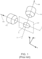
- Figure 1 is a schematic view of a conventional configuration for a microscope employed to perform selective plane illumination microscopy (SPIM) on a sample S.
- the x-axis and y-axis are taken to lie in a transverse plane.
- the sample S, or at least a slice of the sample S being illuminated lies in a sample plane that in the present context corresponds to (or is parallel with) the transverse plane.
- the z-axis is taken to be the axis or direction that is orthogonal to the transverse plane and thus the sample plane. Accordingly, the thickness of the sample S is defined along the z-axis (or z-direction).
- the conventional SPIM microscope includes illumination optics defining an illumination light path for illumination light 104 to propagate generally along an illumination axis I, and detection optics defining a detection light path for detection light 108 to propagate generally along a detection axis D.
- the illumination optics include an illumination objective lens 112 as well as other optical components, and the detection optics include a detection objective lens 116 as well as other optical components, as appreciated by persons skilled in the art.
- the detection objective lens 116 has a focal plane FP (in the transverse x-y plane) at which in-focus images can be acquired by the light detector (not shown) that receives the detection light 108.
- the illumination optics are configured to focus the illumination light 104 into a thin, planar light sheet, i.e., a beam with a substantially rectilinear cross-section.
- Figure 2 is a schematic view of a light sheet 220, or more specifically a portion of the light sheet 220 (its length along the z-axis truncated) in the region where the sample S is positioned.
- the illumination axis I (along the x-axis) along which the light sheet 220 propagates is orthogonal to the detection axis D (along the z-axis) along which the detection light 108 propagates.
- the sample S is positioned and oriented such that the sample plane lies in the focal plane FP and hence is orthogonal to the detection axis D, and the light sheet 220 propagates along the focal plane FP (and thus the sample plane) as the light sheet 220 passes through the sample S.
- SPIM in effect optically sections the sample S, i.e., only a small part of the thickness (in the direction of the z-axis) of the sample S is illuminated by the light sheet 220.
- the thickness of the light sheet 220 (in the direction of the z-axis) converges to a focal point, or "beam waist" 224, and then diverges back to a larger thickness.
- the illumination optics position the light sheet 220 so that the beam waist 224 is in the sample chamber (not shown) containing the sample S and at the focal plane FP.
- the beam waist 224 is positioned at the center of the field of view (FOV) of the detection objective lens 116 and in a central region of the sample S.
- FOV field of view
- SPIM In comparison to other conventional techniques such as wide-field and confocal microscopy, because SPIM exposes the sample S to only the thin light sheet 220 (a thin volume or section of the sample S around the sample plane/focal plane FP), SPIM can image the sample S with less risk of photo-bleaching, photo-damage (e.g., photo-toxicity), and heating.
- SPIM has disadvantages.
- FIG. 3D imaging requires scanning the sample S (or scanning the focal plane FP) along the detection axis D to acquire multiple (essentially 2D) images incrementally (step-wise) and thereby produce a stack of images (z-stack), followed by post-processing to render a 3D image from the multiple 2D images.
- Figure 3 is a schematic illustration of the process of scanning the thickness of the sample S to acquire multiple images for 3D processing in conventional SPIM. The sample S is scanned through multiple positions on the detection axis D, in one or both directions along the as indicated by a double-headed arrow in Figure 3 .
- the sample S is scanned, typically by motorized means, by either moving (translating) the sample S along the detection axis D relative to the illumination axis I or moving the illumination axis I relative to the sample S.
- Figure 3 illustrates three translational positions A, B, and C at which the illumination axis I (and focal plane FP, Figure 1 ) may be positioned as part of scanning the sample S to build a z-stack for 3D processing.
- a separate image must be acquired at each position A, B, and C and digitally stored. Then all of the images so acquired must be processed by executing various software-implemented algorithms to construct the 3D image. It will be noted that illustration of only three translational positions A, B, and C is a simplification, and that many more images are acquired (e.g., 100) during the scanning process.
- Another disadvantage is that light sheet illumination can cause shadow artifacts or stripes to appear in the image, due to the light sheet 220 entering the sample S from one side and encountering opaque structures as the light sheet 220 passes through the sample S toward the other side. See Santi, Peter A., Light Sheet Fluorescence Microscopy: A Review, Journal of Histochemistry & Cytochemistry, Vol. 59(2), p. 129-138 (2011 ); and U.S. Patent No. 9,134,521 Also, the sample plane can be unevenly illuminated due to the light sheet 220 entering the sample S from one side only.
- the portion of the sample plane closest to the side at which the light sheet 220 enters is better illuminated in comparison to the portion of the sample plane farthest from the side at which the light sheet 220 enters, due to light absorption as the light sheet 220 passes through the sample S.
- a "dual-sided illumination" technique has been developed to address these problems, by adding a second illumination objective lens on the side of the sample opposite to the first illumination objective lens 112 and irradiating the sample S with a second light sheet of illumination light 104.
- the additional illumination light path increases the cost and complexity of the microscope.
- dual-sided illumination increases light scattering in the z-direction (along the detection axis D, through the thickness of the sample S), which increases out-of-focus illumination and thus degrades image quality.
- mSPIM multi-directional SPIM
- the mSPIM technique also entails rotating the sample S about the detection axis D to different angular positions, thus further multiplying the number of separate images that must be required and further increasing the cost and complexity of the microscope. Moreover, it can be difficult to align two or more light sheets properly relative to the sample plane, which impairs the ability to acquire a well-focused image.
- SPIM techniques such as those just described typically employ a sample chamber filled with a liquid such as a physiological solution or a clearing solution.
- the sample S is attached to a rod that is inserted into the chamber, and which is attached to the stages operated to translate and rotate the sample S.
- sample supports commonly found in the laboratory such as glass microscope slides, multi-well microplates, and other sample containers.
- an "illumination from the side" technique is not feasible.
- the present disclosure provides a microscope configured to implement a fast three-dimensional (3D) imaging technique based on light-field imaging in comparison to conventional imaging techniques that capture only light intensity information.
- a microscope as disclosed herein combines light-field imaging with a selective illumination method that utilizes a light sheet in a substantially different manner in comparison to conventional SPIM techniques such as described above.
- One or more embodiments of a microscope as disclosed herein may be fluorescence-based.
- One or more embodiments of a microscope as disclosed herein may be particularly useful for producing image data from complex and functional biological samples such as organoids and spheroids.
- One or more embodiments of a microscope as disclosed herein may utilize certain microscope components that are readily available, and may be compatible with different types of sample supports such as, for example, microscope slides, multi-well microplates, and other types of sample containers such as vials, cuvettes, test tubes, sample cells, flow cells, etc.
- a microscope as disclosed herein may be set up in an epi-fluorescence configuration.
- a microscope as disclosed herein may be provided as a stand-alone instrument or may be integrated with other types of analytical instruments such as, for example, multimode readers configured for carrying out different types of optical-based (e.g., fluorescence, luminescence, and absorbance) measurements on samples.
- optical-based e.g., fluorescence, luminescence, and absorbance
- Figure 4 is a schematic view of an example of a light-field microscope 400 according to a representative embodiment disclosed herein.
- a light-field microscope 400 according to a representative embodiment disclosed herein.
- the structure and operation of various types of microscopes are understood by persons skilled in the art, and thus certain components and features of the microscope 400 are described only briefly to facilitate an understanding of the subject matter taught herein.
- the microscope 400 may generally include a light source 424 configured for generating illumination light (excitation light) 404, a sample stage 428 for supporting a sample under analysis (not shown), a light detector (or image sensor) 432 configured for collecting (capturing an image of) detection light (emission light) 408, various illumination optics for defining (i.e., establishing or providing) an illumination (or excitation) light path from the light source 424 to the sample at the sample stage 428, and various detection optics for defining a detection (or emission) light path from the sample to the light detector 432.
- the microscope 400 may be configured for exciting the sample at a specific excitation wavelength and detecting fluorescent light emitted from the sample at a longer wavelength in response to the excitation.
- a fluorescent agent or fluorophore e.g., fluoroscein
- the microscope 400 may be set up in an epi-fluorescence configuration as illustrated in Figure 4 .
- the microscope 400 may be configured for detecting light reflected or scattered from (or transmitted through) the sample generally at the same wavelength as the light utilized to illuminate the sample.
- the light source 424 may be any light source suitable for light (optical) microscopy.
- the light source 424 may be a solid-state light source such as a light emitting diode (LED) or a solid-state laser, or alternatively may be a semiconductor-based laser (laser diode or LD).
- the light source 424 may include a plurality of light sources (e.g., multiple LEDs) that generate light at different wavelengths.
- Such light sources may be mounted to wavelength selector, such as a motorized wheel (not shown) that enables automatic (computerized) selection of the light source and thus the wavelength of the excitation light to be utilized in a given application, as appreciated by persons skilled in the art.
- the light source 424 may be a broadband light source that operates in conjunction with an excitation filter 436 that only allows the desired excitation wavelength of light to pass.
- the sample stage 428 is schematically depicted as a sample plane at which the sample is positioned and supported by the sample stage 428.
- the sample stage 428 may generally be any platform for supporting a sample, or a sample and a substrate supporting the sample (e.g., a microscope slide, microplate, other container), in a fixed position thereon.
- the x-axis and y-axis are taken to lie in a transverse plane, and the z-axis is taken to be the axis or direction that is orthogonal to the transverse plane and thus the sample plane. Accordingly, the thickness of the sample is defined along the z-axis (or z-direction).
- the sample stage 428 (and thus the sample thereon) may be movable by manual or motorized actuation, e.g., by utilizing controlled precision micro-motors as appreciated by persons skilled in the art. That is, the position of the sample stage 108 may be adjustable by the user along the x-axis, y-axis, and/or z-axis.
- an arrow above the sample stage 428 indicates movement along the x-axis.
- the sample stage 108 may be rotatable about one or more axes.
- the light detector 432 may be any imaging device suitable for light microscopy such as, for example, the type of imaging device that forms the basis of cameras.
- the light detector 432 is a multi-pixel (or pixelated) imaging device such as, for example, a charge-coupled device (CCD) or an active-pixel sensor (APS) based on complementary metal-oxide-semiconductor (CMOS) technology.
- the microscope 400 may also include an eyepiece or ocular lens (not separately shown) to enable the user to view the sample, in which case appropriate optical components (e.g., beam splitter) are provided to split the detection light path so that the detection light 408 is directed to both the light detector 432 and the eyepiece.
- the light detector 432 in Figure 1 may be considered as schematically representing an imaging device, or both an imaging device and an eyepiece.
- optics (optical components) defining the illumination light path include a condenser lens 440, a light-sheet focusing device such as a cylindrical lens 444, a beam splitter 448 (e.g., a dichroic beam splitter or mirror), the excitation filter 436 (particularly in fluorescence-based embodiments), and an objective lens 452.
- other optics may be included such as, for example, other lenses (e.g., collimating lenses, relay lenses, field lenses, etc., a beam expander, other mirrors, etc.), as appreciated by persons skilled in the art.
- an aperture stop and a field stop may be included may be positioned between the light source 424 and the condenser lens 440 to limit the transmission of the illumination light 404 emitted by the light source 424 in the x-direction and the y-direction.
- the condenser lens 440 may be any lens configured for collecting the illumination light 404 generated by the light source 424 and concentrating the illumination light 404.
- the cylindrical lens 444 may be any lens configured for focusing the illumination light 404 received from the condenser lens 440 into a thin, planar light sheet 456.
- the light sheet 456 is characterized by having a generally rectilinear cross-section, with one dimension of the cross-section (e.g., length) being substantially greater than the other dimension of the cross-section (e.g., width), as described above in conjunction with Figure 2 .
- the light sheet 456 is utilized for selective illumination of the sample along its thickness, as described further below.
- a beam expander may be placed in the illumination light path between the light source 424 and the cylindrical lens 444 to more completely fill the cylindrical lens 444.
- a suitable alternative may be a slit such as may be provided at an aperture stop.
- the beam splitter 448 is included in some embodiments, particularly in embodiments employing an epi-fluorescence setup as illustrated in Figure 1 .
- the beam splitter 448 is configured to reflect light at the wavelengths contemplated for the illumination light 404 and to transmit light at the wavelengths contemplated for the detection light 408.
- the beam splitter 448 may include a plurality of beam splitters having different optical reflection/transmission characteristics. Such beam splitters may be mounted to wavelength selector, such as a motorized wheel (not shown) that enables automatic (computerized) selection of the beam splitter with the desired reflection/transmission spectrum.
- the beam splitter 448 may be movable, i.e., the position of the beam splitter 448 may be adjustable.
- the beam splitter 448 is rotatable about the x-axis as indicated by the curved arrow in Figure 4 , enabling the angle of the illumination axis I relative to the sample plane to be adjusted.
- the illumination axis I is the direction along which the light sheet 456 (illumination light 404) propagates when the light sheet 456 is incident on the sample.
- the angle of the illumination axis I is the angle of incidence of the light sheet 456.
- the illumination axis I is the direction along which the light sheet 456 propagates after being reflected by the beam splitter 448.
- the objective lens 452 may be any device configured for collecting the detection light 408 emanating from the sample and focusing the detection light 408 onto the light detector 432.
- the objective lens 452 is in the illumination light path I as well as the detection light path D, and thus also is configured for transmitting and focusing the illumination light 404 (as a light sheet 456) onto the sample.
- the illumination light axis I after deflection by the beam splitter 448) and the detection light axis D are coincident.
- the objective lens 452 has a pupil 460 in front of the objective lens 452, between the objective lens 452 and the beam splitter 448.
- optics (optical components) defining the detection light path include the objective lens 452, the beam splitter 448 (configured to transmit the detection light 408 therethrough), an emission filter 464 (particularly in fluorescence-based embodiments), a tube lens 468 (particularly in when the objective lens 452 is an infinity-corrected objective lens), and a microlens array 472.
- the microlens array 472 is an array (typically two-dimensional) of closely grouped microlenses or lenslets (lenses having a diameter on the order of micrometers to few millimeters) supported on a suitable substrate.
- the microlens array 472 may be constructed using microfabrication techniques known to persons skilled in the art.
- the microlenses may be circular and arranged in a hexagonal pattern allowing close grouping of the microlenses on the supporting substrate.
- the microlenses may be square and arranged in a grid-like pattern on the supporting substrate.
- the microlenses are plano-convex.
- the microlens array 472 is configured to focus light onto the active sensing elements of the light detector 432 in a manner that allows the light detector 432 to capture the light field associated with the illuminated region of the sample instead of an image based solely on light intensity.
- the microlens array 472 allows the microscope 400 to function as a light-field microscope.
- the light field may be defined in terms of a bundle of light rays, with each light ray having a magnitude (intensity) and a direction.
- the magnitude of a light ray may be given by radiance, i.e. the amount of light traveling along a ray, which may be measured in watts (W) per steradian (sr) per meter squared (m 2 ).
- each light ray may be given by a multidimensional plenoptic function dependent on both spatial coordinates and angles, as appreciated by persons skilled in the art.
- a light ray may be represented by a four-dimensional function L(u,v,s,t), which is a two-plane parameterization by which the light ray is considered to pass through a point on a u-v plane and then pass through a point on an s-t plane.
- L(u,v,s,t) is a two-plane parameterization by which the light ray is considered to pass through a point on a u-v plane and then pass through a point on an s-t plane.
- Information regarding both the position and direction of the light rays is acquired by the light detector 432 and utilized to generate an image of the sample.
- the microlens array 472 may include, for example, thousands or millions of microlenses.
- the number of active sensing elements (e.g., pixels) provided by the light detector 432 is substantially greater than the number of microlenses provided by the microlens array 472, such that a light ray transmitted through one microlens may be sensed by several active sensing elements.
- the microlenses are sized and positioned relative to the sensors of the light detector 432 such that light rays transmitted through adjacent microlenses do not overlap with each other.
- the microlens array 472 may be positioned at an image plane, such as an intermediate image plane created by one of the optical components in the optical train such as the objective lens 452 or the tube lens 468. In some embodiments and as illustrated, the microlens array 472 may be positioned between the tube lens 468 and the light detector 432. In other embodiments, the tube lens 468 is not included and the microlens array 472 in effect replaces the tube lens 468. In some embodiments, the microlens array 472 may be positioned at a distance from the light detector 432 equal to one focal length f of the microlenses of the microlens array 472.
- the focal length f of a lens is the distance from the lens to its focus (the image point at which light rays from the scene converge), as appreciated by persons skilled in the art.
- the f-number of the microlens array 472 matches the f-number of the imaging optics defined by the pupil diameter and the focal length of the tube lens 468.
- the microscope 400 may further include a computing device (or system controller) 476 in electrical communication with the light detector 432.
- the computing device 476 may be configured to receive light-field images captured by the light detector 432, and digitize and record the images.
- the computing device 476 may also be configured to process the captured light-field data as needed for generating 3D images of the sample, such as by executing deconvolution and/or other algorithms useful for 3D rendering.
- the computing device 476 may also be configured to process the 3D images as needed for displaying the images on a display device such as a computer screen, and for enabling a user to enhance or control the display of the images in a desired manner.
- the computing device 476 may include hardware (microprocessor, memory, etc.) and software components as appreciated by persons skilled in the art.
- the computing device 476 may include a processor such as a main electronic processor providing overall control, and one or more electronic processors configured for dedicated control operations or specific signal processing tasks (e.g., a graphics processing unit, or GPU).
- the computing device 476 may also include one or more memories (volatile and/or non-volatile) for storing data and/or software.
- the computing device 476 may also include one or more device drivers for controlling one or more types of user interface devices and providing an interface between the user interface devices and components of the computing device.
- Such user interface devices may include other user output devices (e.g., printer, visual indicators or alerts, audible indicators or alerts, and the like) and also user input devices (e.g., keyboard, keypad, touch screen, mouse controller, joystick, trackball, and the like).
- the computing device 476 may also include one or more types of computer programs or software contained in memory and/or on one or more types of computer-readable media.
- Computer programs or software may contain instructions (e.g., logic instructions) for performing all or part of any of the methods disclosed herein.
- Computer programs or software may include application software and system software.
- Figure 1 is a high-level schematic depiction of an example of the microscope 100 consistent with the present disclosure.
- Other optics, electronics, and mechanical components and structures not specifically shown in Figure 1 may be included as needed for practical implementations, as appreciated by persons skilled in the art.
- the sample under investigation may be prepared for microscopy as needed and then mounted to the sample stage 428.
- the sample is supported on (mounted on, held by, contained in, etc.) a suitable sample support (glass slide, well of a multi-well plate, other type of receptacle, etc.) and the sample support is then mounted to the sample stage 428.
- the light source 424 is then activated to generate illumination light 404, which may be broadband or narrowband light (e.g., centered on a desired wavelength) depending on the embodiment.
- the illumination light 404 is wavelength-filtered by the excitation filter 436.
- the illumination light 404 is directed to and concentrated by the condenser 440.
- the illumination light 404 is then directed to the cylindrical lens 444, which focuses the illumination light 404 into a light sheet 456.
- the illumination light 404 is then reflected by the beam splitter 448 toward the sample, whereby the illumination light 404 propagates as the along the illumination axis I (z-axis).
- the angle of the illumination axis relative to the sample plane is dictated by the orientation of the beam splitter 448.
- the illumination light 404 is then focused by the objective lens 452 onto a selected region of the sample.
- the illumination light 404 incident on the sample is still in the form of the light sheet 456.
- the sample In response to the illumination, the sample emits detection light 408, which in the present embodiment is fluorescent light.
- the objective lens 452 collects the detection light 408 and focuses the detection light 408 at an image plane.
- the tube lens 468 if, the tube lens 468 is included, the objective lens 452 transmits the detection light 408 to the tube lens 468 and the tube lens 468 focuses the detection light 408 at the image plane.
- the beam splitter 448 is configured to allow the detection light 408 to pass through the beam splitter 448 without being reflected or attenuated.
- the detection light 408 is wavelength-filtered by the emission filter 464.
- the microlens array 472 positioned at the image plane in the present embodiment, focuses the rays of the detection light 408 onto the active sensing elements of the light detector 432.
- the light detector 432 outputs the light-field image information as electrical signals to the computing device 476, which processes the signals to generate a 3D image of the illuminated region of the sample.
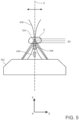
- FIG. 5 is a schematic view of a sample S illuminated by the light sheet 456 in accordance with embodiments disclosed herein.
- the light sheet 456 has a beam waist 524 that may be positioned in the sample S.
- the illumination axis I of the light sheet 456, and thus the plane of illumination, is different from that of conventional SPIM-related techniques such as described above in conjunction with Figures 1-3 .
- the light sheet is directed along an illumination axis that is parallel with the sample (x-y) plane.
- the illumination axis I of the light sheet 456 is oriented in a direction non-parallel with the sample plane.
- the light sheet 456 is oriented at ninety degrees relative to the sample plane, i.e., directly along the z-axis.
- the angle of the light sheet 456 (and thus the illumination axis I) may be in a range from 0 to 180 degrees relative to the sample plane, although in practice the angular range of the light sheet 456 is limited by the physical constraints of the objective lens 452 and/or other components of the optical train.
- the angle of the light sheet 456 (and thus the illumination axis I) may be in a range from 45 to 135 degrees relative to the sample plane.
- the selected plane of illumination provided by the light sheet 456 is directed through the thickness of the sample S (in a selected region of the sample S).
- the microscope 400 provides additional advantages.
- the microscope 400 is set up with a common epi-illumination type of configuration like as shown in Figures 4 and 5 , with the illumination axis I being coincident with the detection axis D.
- Such configuration allows readily available optical components such as objective lenses, beam splitters, etc. to be utilized.
- FIG. 6 is a schematic view of a sample S illuminated by the light sheet 456 while disposed in a container 680, in accordance with embodiments disclosed herein.
- the container 680 may be one of a plurality of containers 680 arranged in an array.
- the containers 680 may be the wells of a microplate, vials or test tubes supported by a rack, etc.
- the sample S may be immersed in a liquid L.
- Other samples may be disposed in the other containers 680, and may be immersed in the same liquid or different liquids, or the same solvent but containing different reagents, or different multi-solvent compositions.
- the side walls of the containers 680, and solid media between adjacent containers 680 do not interfere with the vertical light sheet 456.
- the light sheet 456 may be scanned over a range of angles relative to the sample S without encountering the solid structure of the container 680.
- the microscope 400 acquires light-field data instead of just light intensity data, (at least for most samples of the type to be imaged by the microscope 400) the sample S does not need to be scanned through its thickness along the detection axis D (z-direction). That is, only a single light-field image needs to be acquired, and only digital post-processing needs to be performed (e.g., by the computing device 476) in order to derive a z-stack or otherwise produce a 3D image of the sample S.
- the useable z-range ⁇ z ( Figures 5 and 6 ) is typically 6 to 10 times larger than the depth of field (DOF) of the objective lens 452.
- the nominal DOF is 8 ⁇ m, in which case a typical lightfield acquisition would result in an accessible z-range of approximately 50 ⁇ m, which is a reasonable measure for the imaging of organoids.
- Another limit in ⁇ z is set by the length of the light sheet 456. According to Gaussian optics the light sheet 456 will develop its beam waist 524 in the y dimension at the focal point of the objective lens 452.
- the length of the lightsheet 456 ⁇ z is defined by the maximum acceptable distance ⁇ (1/2) ⁇ z from the beam waist 524.
- the limit is defined by the maximum acceptable beam cross-section as a function of z.
- the length of the light sheet 456 may be up to a few millimeters.
- While embodiments disclosed herein may eliminate the requirement of scanning the sample S in the z-direction, depending on the size of the sample S and/or the field of view (FOV) of the objective lens 452, obtaining image information on the whole sample S may require scanning the sample S through the transverse plane, for example along the x-direction or y-direction. Scanning the sample S may be done by moving (translating and/or rotating) the sample S itself relative to the light sheet 456 and/or by moving (translating and/or rotating) the light sheet 456 relative to the sample S.
- the sample stage 428 may be configured to translate the sample S, as indicated by the arrow above the sample stage 428 in Figure 4 and the arrow above the sample S in Figure 5 .
- the beam splitter 448 (or “scanning mirror”), or other beam-steering component in the illumination light path, may be configured to rotate (as indicated by a curved arrow in Figure 4 ) so as to scan the light sheet 456 through the sample, in this case by adjusting the angle of incidence of the light sheet 456 on the sample.
- Figure 7 is a schematic view of an example of a light-field microscope 700 (or a portion thereof) according to another embodiment.
- the microscope 700 may include components that are the same or similar to those of the microscope 400 described above and illustrated in Figure 4 .
- the scanning mirror 448 is positioned at the pupil of the objective lens 452. This configuration as the advantage of maintaining the telecentric condition.
- Microscope optics benefit from being telecentric by providing a constant viewing angle (preferably 90°) onto the specimen across the entire field. Consequently, for SPIM this means a constant inclination angle of the lightsheet 456 with respect to the specimen across the entire field.
- One or more additional mirrors 784 may be provided in the illumination light path to provide spatial accommodation for the optics of the detection light path not shown in Figure 7 , for example the emission filter 464, tube lens 468, microlens array 472, and light detector 432 described above and illustrated in Figure 4 .
- Either the scanning mirror 448 or another mirror 784 may be configured as a beam splitter, and the optics of the detection light path may be positioned accordingly.
- Figure 8 is a schematic view of an example of a light-field microscope 800 according to another embodiment.
- the microscope 800 may include components that are the same or similar to those of the microscope 400 described above and illustrated in Figure 4 .
- the microscope 800 includes a light source 824 configured for generating a plurality of illumination light beams 804, which are then focused as a plurality of light sheets 856 onto the sample.
- the sample may emit a plurality of detection light beams 808.
- the light source 824 may, for example, include a plurality of point sources (e.g., multiple LEDs or laser emitters), or one or more light sources directing light to a plurality of pinholes or slits positioned at an aperture stop between the light source(s) and the condenser lens 440. When slits are provided, the cylindrical lens 444 may not be needed.
- the light source 824 may include an active projection device such as may include or be based on a digital micromirror device (DMD), a liquid crystal on silicon (LCoS) device, or a liquid crystal display (LCD) device.
- DMD digital micromirror device
- LCD liquid crystal on silicon
- Figure 9 is a schematic view of an example of a light-field microscope 900 according to another embodiment.
- the microscope 900 may include components that are the same or similar to those of the microscope 400 described above and illustrated in Figure 4 .
- the microscope 900 has a focused Galilean configuration. This approach enables enhancements in terms of lateral resolution compared to configuration of the microscope 400 shown in Figure 4 , by exploiting the details in the microimages formed by the microlens array 472 at the detector position.
- reconstruction algorithms are different compared to those used for the microscope 400 and rely on stereographic projection based on correspondences.
- the term "Galilean" refers to the optical layout of the microscope 900, which has similarities to a Galilean type telescope.
- the microlens array 472 may completely replace the tube lens 468.
- Figure 10 is a schematic view of an example of a light-field microscope 1000 according to another embodiment.
- the microscope 1000 may include components that are the same or similar to those of the microscope 400 described above and illustrated in Figure 4 .
- the microscope 1000 has a focused Keplerian configuration.
- the optical layout of this configuration relates to a Keplerian type telescope, but in terms of optical performance the same benefits as for the Galilean type apply.
- the pros with respect to the Galilean configuration are longer distances. Commonly, this configuration shows greater flexibility when adapted to a given microscope stand.
- the pros of the Galilean configuration are a shorter optical train and that the variation of the effective resolution across the accessible z-range can be controlled better.
- the microlens array 472 may be positioned at a distance from the light detector 432 equal to one focal length f of the microlenses of the microlens array 472.
- the microlens array 472 may be positioned at a distance from the light detector 432 that is less than one focal length f of the microlenses of the microlens array 472.
- the microlens array 472 may be positioned at a distance from the light detector 432 that is greater than one focal length f of the microlenses of the microlens array 472.
- the intermediate image is schematically shown, for example, in Figure 10 as the point just above the microlens array 472 where the rays are depicted as transitioning from converging to diverging.
- the lens-to-image distance d i 20 mm.
- the lens-to-image distance d i 20 mm.
- (1/-20) + (1/ d i ) (3/20).
- the lens-to-image distance d i 6.67 mm.
- the software may reside in a software memory (not shown) in a suitable electronic processing component or system such as, for example, the system controller (computing device) 476 schematically depicted in Figure 4 .
- the software memory may include an ordered listing of executable instructions for implementing logical functions (that is, "logic" that may be implemented in digital form such as digital circuitry or source code, or in analog form such as an analog source such as an analog electrical, sound, or video signal).
- the instructions may be executed within a processing module, which includes, for example, one or more microprocessors, general purpose processors, combinations of processors, digital signal processors (DSPs), application specific integrated circuits (ASICs), or field-programmable gate arrays (FPGAs).
- a processing module includes, for example, one or more microprocessors, general purpose processors, combinations of processors, digital signal processors (DSPs), application specific integrated circuits (ASICs), or field-programmable gate arrays (FPGAs).
- DSPs digital signal processors
- ASICs application specific integrated circuits
- FPGAs field-programmable gate arrays
- the executable instructions may be implemented as a computer program product having instructions stored therein which, when executed by a processing module of an electronic system (e.g., the system controller 476 shown in Figure 4 ), direct the electronic system to carry out the instructions.
- the computer program product may be selectively embodied in any non-transitory computer-readable storage medium for use by or in connection with an instruction execution system, apparatus, or device, such as an electronic computer-based system, processor-containing system, or other system that may selectively fetch the instructions from the instruction execution system, apparatus, or device and execute the instructions.
- a computer-readable storage medium is any non-transitory means that may store the program for use by or in connection with the instruction execution system, apparatus, or device.
- the non-transitory computer-readable storage medium may selectively be, for example, an electronic, magnetic, optical, electromagnetic, infrared, or semiconductor system, apparatus, or device.
- a non-exhaustive list of more specific examples of non-transitory computer readable media include: an electrical connection having one or more wires (electronic); a portable computer diskette (magnetic); a random access memory (electronic); a read-only memory (electronic); an erasable programmable read only memory such as, for example, flash memory (electronic); a compact disc memory such as, for example, CD-ROM, CD-R, CD-RW (optical); and digital versatile disc memory, i.e., DVD (optical).
- non-transitory computer-readable storage medium may even be paper or another suitable medium upon which the program is printed, as the program can be electronically captured via, for instance, optical scanning of the paper or other medium, then compiled, interpreted, or otherwise processed in a suitable manner if necessary, and then stored in a computer memory or machine memory.
- the term "in signal communication" as used herein means that two or more systems, devices, components, modules, or sub-modules are capable of communicating with each other via signals that travel over some type of signal path.
- the signals may be communication, power, data, or energy signals, which may communicate information, power, or energy from a first system, device, component, module, or sub-module to a second system, device, component, module, or sub-module along a signal path between the first and second system, device, component, module, or sub-module.
- the signal paths may include physical, electrical, magnetic, electromagnetic, electrochemical, optical, wired, or wireless connections.
- the signal paths may also include additional systems, devices, components, modules, or sub-modules between the first and second system, device, component, module, or sub-module.
Landscapes
- Physics & Mathematics (AREA)
- General Physics & Mathematics (AREA)
- Optics & Photonics (AREA)
- Chemical & Material Sciences (AREA)
- Analytical Chemistry (AREA)
- Engineering & Computer Science (AREA)
- Multimedia (AREA)
- Computer Vision & Pattern Recognition (AREA)
- Health & Medical Sciences (AREA)
- General Engineering & Computer Science (AREA)
- Nuclear Medicine, Radiotherapy & Molecular Imaging (AREA)
- Life Sciences & Earth Sciences (AREA)
- Biochemistry (AREA)
- General Health & Medical Sciences (AREA)
- Immunology (AREA)
- Pathology (AREA)
- Microscoopes, Condenser (AREA)
- Investigating, Analyzing Materials By Fluorescence Or Luminescence (AREA)
Claims (15)
- Microscope à champ lumineux (400), comprenant :une source de lumière (424) configurée pour générer une lumière d'éclairage (404) ;une lentille de condenseur (440) configurée pour recevoir la lumière d'éclairage (404) à partir de la source de lumière (424) et émettre la lumière d'éclairage sous la forme de lumière d'éclairage focalisée ;un dispositif de focalisation de feuille de lumière (444) configuré pour recevoir la lumière d'éclairage focalisée à partir de la lentille de condenseur (440) et émettre la lumière d'éclairage sous la forme de feuille de lumière (456) sur un axe d'éclairage (I) ;une platine d'échantillon (428) configurée pour supporter un échantillon dans un plan d'échantillon et pour recevoir la feuille de lumière (456) le long de l'axe d'éclairage (I) qui est non parallèle au plan d'échantillon ;une lentille d'objectif (452) configurée pour recevoir une lumière de détection à partir de l'échantillon sur un axe de lumière de détection (D) ;un réseau de micro-lentilles (472) configuré pour recevoir la lumière de détection à partir de la lentille d'objectif (452) ; etun détecteur de lumière (432) configuré pour recevoir la lumière de détection à partir du réseau de micro-lentilles (472) et mesurer des paramètres de champ lumineux de la lumière de détection,caractérisé en ce quel'axe de lumière de détection (D) et l'axe de lumière d'éclairage (I) coïncident.
- Microscope à champ lumineux selon la revendication 1, dans lequel la source de lumière (424) est configurée pour générer la lumière d'éclairage à une longueur d'onde efficace pour induire une lumière de détection fluorescente à partir de l'échantillon.
- Microscope à champ lumineux selon la revendication 1 ou la revendication 2, dans lequel la source de lumière (424, 824) est configurée pour générer une pluralité de faisceaux lumineux d'éclairage (804), et le dispositif de focalisation de feuille de lumière (444) est configuré pour émettre la pluralité de faisceaux lumineux d'éclairage sous la forme d'une pluralité de feuilles de lumière (456, 856).
- Microscope à champ lumineux selon la revendication 1, la revendication 2 ou la revendication 3, dans lequel le dispositif de focalisation de feuille de lumière (444) est sélectionné parmi le groupe constitué de : une lentille cylindrique ; et une ouverture comprenant une ou plusieurs fentes.
- Microscope à champ lumineux selon l'une quelconque des revendications précédentes, comprenant un élément optique (448) configuré pour définir au moins une partie d'un trajet de lumière d'éclairage à partir de la source de lumière (424) vers l'échantillon, et pour définir au moins une partie d'un trajet de lumière de détection à partir de l'échantillon vers le détecteur de lumière (432) ;
dans lequel en particulier :l'élément optique comprend un miroir dichroïque (448) configuré pour recevoir la feuille de lumière (456) et réfléchir la feuille de lumière en direction de l'échantillon, et pour recevoir la lumière de détection et transmettre la lumière de détection en direction du détecteur de lumière (432), oula lentille d'objectif (452) est positionnée à la fois dans le trajet de lumière d'éclairage et dans le trajet de lumière de détection, oul'élément optique (448) comprend un miroir mobile configuré pour régler un angle de la direction d'éclairage par rapport au plan d'échantillon, dans lequel le miroir mobile est facultativement positionné au niveau d'une pupille de la lentille d'objectif (452). - Microscope à champ lumineux selon l'une quelconque des revendications précédentes, dans lequel la platine d'échantillon (428) est configurée pour translater l'échantillon dans le plan d'échantillon, ou pour faire tourner le plan d'échantillon par rapport à la feuille de lumière (456), ou les deux.
- Microscope à champ lumineux selon l'une quelconque des revendications précédentes, dans lequel la platine d'échantillon (428) est configurée pour supporter un réseau de récipients d'échantillon (680).
- Microscope à champ lumineux selon l'une quelconque des revendications précédentes, dans lequel le réseau de micro-lentilles (472) est positionné au niveau d'un plan d'image.
- Microscope à champ lumineux selon l'une quelconque des revendications précédentes, dans lequel le détecteur de lumière (432) est positionné à une distance du réseau de micro-lentilles (472)égale à une longueur focale de micro-lentilles du réseau de micro-lentilles, oude sorte que le microscope à champ lumineux présente une configuration galiléenne ou képlérienne.
- Microscope à champ lumineux selon l'une quelconque des revendications précédentes, comprenant une lentille tubulaire (468) entre la lentille d'objectif (452) et le réseau de micro-lentilles (472), dans lequel en particulier le nombre f du réseau de micro-lentilles (472) correspond au nombre f d'éléments optiques d'imagerie définis par le diamètre de pupille et la longueur focale de la lentille tubulaire (468).
- Procédé d'acquisition d'une image de champ lumineux à partir d'un échantillon, le procédé comprenant :le support de l'échantillon dans un plan focal d'une lentille d'objectif (452) ;la génération d'une lumière d'éclairage (404) ;la focalisation de la lumière d'éclairage (404) sous la forme d'une feuille de lumière (456) ;l'irradiation de l'échantillon par orientation de la feuille de lumière (456) vers l'échantillon le long d'un axe d'éclairage (I) non parallèle au plan d'échantillon, dans lequel, en réponse à l'irradiation, l'échantillon émet une lumière de détection sur un axe de lumière de détection (D) ;l'orientation de la lumière de détection à travers un réseau de micro-lentilles (472) vers un détecteur de lumière (432) ; etla mesure de paramètres de champ lumineux de la lumière de détection au niveau du détecteur de lumière (432) ;dans lequel l'axe de lumière de détection (D) et l'axe de lumière d'éclairage (I) coïncident.
- Procédé selon la revendication 11, comprenant la génération d'une image tridimensionnelle de l'échantillon sur la base des paramètres de champ lumineux mesurés, et/ou
dans lequel l'échantillon présente une épaisseur le long de la direction d'éclairage, et comprenant en outre la génération d'une image tridimensionnelle de l'échantillon sur la base des paramètres de champ lumineux mesurés sans balayage de l'échantillon le long de la direction d'éclairage. - Procédé selon la revendication 11 ou la revendication 12, dans lequel la direction d'éclairage est dans une plage de 45 à 135 degrés par rapport au plan d'échantillon.
- Procédé selon la revendication 11, la revendication 12 ou la revendication 13, comprenant :le réglage d'un angle de la direction d'éclairage par rapport au plan d'échantillon, oule balayage de l'échantillon le long du plan d'échantillon, oule support de l'échantillon dans un récipient (680) pendant la mesure des paramètres de champ lumineux.
- Procédé selon l'une quelconque des revendications 11 à 14, dans lequel l'irradiation de l'échantillon comprend la réflexion de la lumière d'éclairage à partir d'un miroir dichroïque (448) en direction de l'échantillon, et l'orientation de la lumière de détection comprend la transmission de la lumière de détection à travers le miroir dichroïque.
Applications Claiming Priority (2)
| Application Number | Priority Date | Filing Date | Title |
|---|---|---|---|
| US15/266,310 US10690898B2 (en) | 2016-09-15 | 2016-09-15 | Light-field microscope with selective-plane illumination |
| PCT/IB2017/055599 WO2018051283A1 (fr) | 2016-09-15 | 2017-09-15 | Microscope à champ lumineux à éclairage sélectif dans un plan |
Publications (2)
| Publication Number | Publication Date |
|---|---|
| EP3513241A1 EP3513241A1 (fr) | 2019-07-24 |
| EP3513241B1 true EP3513241B1 (fr) | 2025-04-23 |
Family
ID=60051549
Family Applications (1)
| Application Number | Title | Priority Date | Filing Date |
|---|---|---|---|
| EP17781545.3A Active EP3513241B1 (fr) | 2016-09-15 | 2017-09-15 | Microscope à champ lumineux à éclairage sélectif dans un plan |
Country Status (5)
| Country | Link |
|---|---|
| US (1) | US10690898B2 (fr) |
| EP (1) | EP3513241B1 (fr) |
| JP (1) | JP7055793B2 (fr) |
| CN (1) | CN109716199A (fr) |
| WO (1) | WO2018051283A1 (fr) |
Families Citing this family (36)
| Publication number | Priority date | Publication date | Assignee | Title |
|---|---|---|---|---|
| FR3028616A1 (fr) * | 2014-11-13 | 2016-05-20 | Commissariat Energie Atomique | Procede d'analyse comprenant la determination d'une position d'une particule biologique. |
| EP3420535B1 (fr) * | 2016-02-26 | 2022-09-07 | University Of Southern California | Imagerie volumétrique optimisée à éclairage de volume sélectif et détection de champ lumineux |
| WO2017180680A1 (fr) * | 2016-04-12 | 2017-10-19 | The Board Of Regents Of The University Of Texas System | Microscope à feuille de lumière avec acquisition d'images 3d parallélisées |
| CN106990519B (zh) * | 2017-05-12 | 2024-09-24 | 中国科学院苏州生物医学工程技术研究所 | 结构光照明显微成像系统 |
| JP6932036B2 (ja) * | 2017-07-31 | 2021-09-08 | シスメックス株式会社 | 細胞撮像方法、細胞撮像装置、粒子撮像方法および粒子撮像装置 |
| WO2019148008A1 (fr) * | 2018-01-26 | 2019-08-01 | University Of Washington | Appareils et procédés de microscopie à feuille de lumière à balayage numérique à directions multiples |
| JP7298993B2 (ja) | 2018-04-09 | 2023-06-27 | 浜松ホトニクス株式会社 | 試料観察装置及び試料観察方法 |
| WO2020150239A1 (fr) * | 2019-01-14 | 2020-07-23 | University Of Washington | Appareils, systèmes et procédés pour lentilles convexo-concaves à immersion solide |
| US11030776B2 (en) * | 2019-02-01 | 2021-06-08 | Molecular Devices (Austria) GmbH | Calibration of a light-field imaging system |
| WO2020161826A1 (fr) * | 2019-02-06 | 2020-08-13 | オリンパス株式会社 | Dispositif d'imagerie |
| CN110687670B (zh) * | 2019-10-16 | 2022-02-08 | 锘海生物科学仪器(上海)有限公司 | 平铺光片显微镜及其使用方法 |
| US10895727B1 (en) * | 2019-10-19 | 2021-01-19 | SequLITE Genomics US, Inc. | Microscope for locating structures on the inner surface of a fluidic channel |
| CN110836892B (zh) * | 2019-11-26 | 2021-06-11 | 清华大学 | 衍射超分辨显微成像方法及系统 |
| EP3839596B1 (fr) * | 2019-12-20 | 2023-08-23 | Euroimmun Medizinische Labordiagnostika AG | Dispositif et procédé d'identification de zones de verre de recouvrement d'une lame porte-objet |
| WO2021166069A1 (fr) * | 2020-02-18 | 2021-08-26 | オリンパス株式会社 | Microscope à feuille de lumière, procédé de commande et programme |
| US20210325652A1 (en) * | 2020-04-21 | 2021-10-21 | University Of Central Florida Research Foundation, Inc. | Instantaneous non-diffracting light sheets |
| EP3929567A1 (fr) | 2020-06-25 | 2021-12-29 | Leica Microsystems CMS GmbH | Procédé et dispositif pour l'examen optique d'un échantillon biologique |
| DE102020128524A1 (de) * | 2020-10-29 | 2022-05-05 | Carl Zeiss Microscopy Gmbh | Lichtblattmikroskop und Verfahren der Lichtblattmikroskopie |
| JP7206020B2 (ja) * | 2020-11-17 | 2023-01-17 | マシンビジョンライティング株式会社 | 画像観察装置及びその照明光学系 |
| KR102469852B1 (ko) * | 2020-11-20 | 2022-11-22 | 충북대학교 산학협력단 | 집적 영상 현미경의 조명계 시스템 |
| CN113040713A (zh) * | 2021-03-08 | 2021-06-29 | 合肥视涯技术有限公司 | 一种口腔扫描仪及口腔扫描方法 |
| CN113552100B (zh) * | 2021-06-23 | 2024-07-02 | 河海大学常州校区 | 一种自动化荧光切片显微成像平台及其操作方法 |
| WO2023007827A1 (fr) * | 2021-07-26 | 2023-02-02 | 浜松ホトニクス株式会社 | Dispositif d'observation d'échantillon et procédé d'observation d'échantillon |
| CN115704776B (zh) * | 2021-08-17 | 2025-08-05 | 中国科学院长春光学精密机械与物理研究所 | 体液分析仪 |
| EP4419893A4 (fr) * | 2021-10-20 | 2025-08-06 | Bio Rad Laboratories Inc | Système de détection de fluorescence |
| CN113768472B (zh) * | 2021-11-10 | 2022-03-22 | 华中科技大学 | 一种具有荧光标记的三维图像获取装置及方法 |
| JP2024546080A (ja) * | 2021-12-02 | 2024-12-17 | エンスペクトラ・ヘルス・インコーポレイテッド | 光操作のためのシステム及び方法 |
| CN114280766A (zh) * | 2021-12-24 | 2022-04-05 | 哈尔滨工业大学 | 基于梯度折射率透镜的七目微型三维显微成像装置和方法 |
| KR102891293B1 (ko) * | 2022-03-31 | 2025-12-01 | 포항공과대학교 산학협력단 | 신속 광학 조직 스캐너 및 스캐닝 방법 |
| WO2025106923A1 (fr) * | 2023-11-15 | 2025-05-22 | The Regents Of The University Of California | Systèmes et procédés de microscopie à éclairage spatio-temporel multi-puits à haut débit |
| CN117631249B (zh) * | 2024-01-18 | 2024-05-24 | 清华大学 | 线扫共聚焦扫描光场显微成像装置及方法 |
| CN118567082B (zh) * | 2024-03-22 | 2025-11-11 | 清华大学 | 三维显微成像装置及其成像方法 |
| CN118333914B (zh) * | 2024-06-05 | 2024-09-03 | 浙江荷湖科技有限公司 | 一种高动态范围的光场数据白图像校正方法、系统及介质 |
| TWI912813B (zh) * | 2024-06-28 | 2026-01-21 | 友達光電股份有限公司 | 自適應調整之光學取像架構 |
| CN119643527B (zh) * | 2024-12-18 | 2025-12-05 | 甬江实验室 | 细胞通讯信号采集方法及系统 |
| CN120065491A (zh) * | 2025-02-25 | 2025-05-30 | 华中科技大学 | 一种基于光场重构的可变倍单物镜光片显微系统 |
Family Cites Families (19)
| Publication number | Priority date | Publication date | Assignee | Title |
|---|---|---|---|---|
| WO2006039486A2 (fr) | 2004-10-01 | 2006-04-13 | The Board Of Trustees Of The Leland Stanford Junior University | Agencements d'imagerie et procedes associes |
| DE102005027077C5 (de) | 2004-11-04 | 2021-01-28 | Leica Microsystems Cms Gmbh | Lichtscheibenmikroskop |
| US9134521B2 (en) | 2008-07-30 | 2015-09-15 | The Regents Of The University Of California | Multidirectional selective plane illumination microscopy |
| US8315476B1 (en) | 2009-01-20 | 2012-11-20 | Adobe Systems Incorporated | Super-resolution with the focused plenoptic camera |
| ATE551841T1 (de) | 2009-04-22 | 2012-04-15 | Raytrix Gmbh | Digitales bildgebungsverfahren zum synthetisieren eines bildes unter verwendung der mit einer plenoptischen kamera aufgezeichneten daten |
| DE102009044987A1 (de) | 2009-09-24 | 2011-03-31 | Carl Zeiss Microimaging Gmbh | Mikroskop |
| US10051240B2 (en) * | 2010-06-14 | 2018-08-14 | Howard Hughes Medical Institute | Structured plane illumination microscopy |
| DE102010044013A1 (de) * | 2010-11-16 | 2012-05-16 | Carl Zeiss Microimaging Gmbh | Tiefenauflösungsgesteigerte Mikroskopie |
| US9316824B2 (en) | 2011-03-04 | 2016-04-19 | The United States Of America, As Represented By The Secretary, Department Of Health And Human Services | Optomechanical module for converting a microscope to provide selective plane illumination microscopy |
| DE102013211426A1 (de) * | 2013-06-18 | 2014-12-18 | Leica Microsystems Cms Gmbh | Verfahren und optische Vorrichtung zum mikroskopischen Untersuchen einer Vielzahl von Proben |
| US10539772B2 (en) * | 2013-10-09 | 2020-01-21 | Howard Hughes Medical Institute | Multiview light-sheet microscopy |
| JP2015135463A (ja) * | 2013-12-19 | 2015-07-27 | オリンパス株式会社 | 顕微鏡装置、及び、顕微鏡システム |
| JP6253400B2 (ja) * | 2013-12-26 | 2017-12-27 | オリンパス株式会社 | 画像形成方法、及び、画像形成装置 |
| DE102014102215A1 (de) | 2014-02-20 | 2015-08-20 | Carl Zeiss Microscopy Gmbh | Verfahren und Anordnung zur Lichtblattmikroskopie |
| US20160041099A1 (en) * | 2014-08-06 | 2016-02-11 | University Of Oregon | Light sheet fluorescence and differential interference contrast microscope |
| DE102014116174A1 (de) * | 2014-11-06 | 2016-05-12 | Carl Zeiss Microscopy Gmbh | Verfahren zur Erzeugung eines Bildes einer Probe |
| JP6555803B2 (ja) * | 2015-06-09 | 2019-08-07 | オリンパス株式会社 | シート照明顕微鏡、及び、シート照明顕微鏡の照明方法 |
| JP6491578B2 (ja) * | 2015-09-07 | 2019-03-27 | オリンパス株式会社 | シート照明顕微鏡システム、画像処理装置、シート照明顕微鏡法、及び、プログラム |
| JP7109423B2 (ja) * | 2016-08-15 | 2022-07-29 | ライカ マイクロシステムズ シーエムエス ゲゼルシャフト ミット ベシュレンクテル ハフツング | ライトシート顕微鏡 |
-
2016
- 2016-09-15 US US15/266,310 patent/US10690898B2/en active Active
-
2017
- 2017-09-15 JP JP2019515424A patent/JP7055793B2/ja active Active
- 2017-09-15 EP EP17781545.3A patent/EP3513241B1/fr active Active
- 2017-09-15 WO PCT/IB2017/055599 patent/WO2018051283A1/fr not_active Ceased
- 2017-09-15 CN CN201780057049.2A patent/CN109716199A/zh active Pending
Also Published As
| Publication number | Publication date |
|---|---|
| JP7055793B2 (ja) | 2022-04-18 |
| EP3513241A1 (fr) | 2019-07-24 |
| CN109716199A (zh) | 2019-05-03 |
| US20180074305A1 (en) | 2018-03-15 |
| US10690898B2 (en) | 2020-06-23 |
| JP2019530006A (ja) | 2019-10-17 |
| WO2018051283A1 (fr) | 2018-03-22 |
Similar Documents
| Publication | Publication Date | Title |
|---|---|---|
| EP3513241B1 (fr) | Microscope à champ lumineux à éclairage sélectif dans un plan | |
| JP6895284B2 (ja) | 光シート顕微鏡および光シート顕微鏡を作動するための方法 | |
| JP6685977B2 (ja) | 顕微鏡 | |
| US8749882B2 (en) | Low numerical aperture exclusion imaging | |
| US10048478B2 (en) | Optical transmission system for correcting image errors and microscope with such a transmission system | |
| JP6241858B2 (ja) | 共焦点顕微鏡 | |
| US10191263B2 (en) | Scanning microscopy system | |
| US8633432B2 (en) | Reflective focusing and transmissive projection device | |
| CN101893755B (zh) | 使用四棱锥镜产生结构照明的荧光显微方法和装置 | |
| CN107209110B (zh) | 高吞吐量生化筛查 | |
| US20130250088A1 (en) | Multi-color confocal microscope and imaging methods | |
| US20180180867A1 (en) | Microscope and setting support method | |
| WO2018070098A1 (fr) | Dispositif d'observation d'échantillon et procédé d'observation d'échantillon | |
| US20250341712A1 (en) | Apparatuses, systems and methods for solid immersion meniscus lenses | |
| CN108700520A (zh) | 用于高吞吐量成像的方法和设备 | |
| JP6928757B2 (ja) | 光学顕微鏡における画像処理のためのシステムおよび方法 | |
| Nichols et al. | Video-rate scanning confocal microscopy and microendoscopy | |
| JP4602731B2 (ja) | 顕微鏡システム | |
| JP6602855B2 (ja) | ミラーデバイス | |
| EP1806575B1 (fr) | Appareil d'examen | |
| JP2004361086A (ja) | 生体分子解析装置 | |
| Hämäläinen | Selective Plane Illumination Microscope Development and Characterization | |
| JP2025106825A (ja) | 画像観察機能付き分光装置 | |
| JP2017227788A (ja) | 顕微鏡および顕微鏡画像取得方法 |
Legal Events
| Date | Code | Title | Description |
|---|---|---|---|
| STAA | Information on the status of an ep patent application or granted ep patent |
Free format text: STATUS: UNKNOWN |
|
| STAA | Information on the status of an ep patent application or granted ep patent |
Free format text: STATUS: THE INTERNATIONAL PUBLICATION HAS BEEN MADE |
|
| PUAI | Public reference made under article 153(3) epc to a published international application that has entered the european phase |
Free format text: ORIGINAL CODE: 0009012 |
|
| STAA | Information on the status of an ep patent application or granted ep patent |
Free format text: STATUS: REQUEST FOR EXAMINATION WAS MADE |
|
| 17P | Request for examination filed |
Effective date: 20190326 |
|
| AK | Designated contracting states |
Kind code of ref document: A1 Designated state(s): AL AT BE BG CH CY CZ DE DK EE ES FI FR GB GR HR HU IE IS IT LI LT LU LV MC MK MT NL NO PL PT RO RS SE SI SK SM TR |
|
| STAA | Information on the status of an ep patent application or granted ep patent |
Free format text: STATUS: EXAMINATION IS IN PROGRESS |
|
| 17Q | First examination report despatched |
Effective date: 20220908 |
|
| GRAP | Despatch of communication of intention to grant a patent |
Free format text: ORIGINAL CODE: EPIDOSNIGR1 |
|
| STAA | Information on the status of an ep patent application or granted ep patent |
Free format text: STATUS: GRANT OF PATENT IS INTENDED |
|
| INTG | Intention to grant announced |
Effective date: 20241118 |
|
| GRAS | Grant fee paid |
Free format text: ORIGINAL CODE: EPIDOSNIGR3 |
|
| GRAA | (expected) grant |
Free format text: ORIGINAL CODE: 0009210 |
|
| STAA | Information on the status of an ep patent application or granted ep patent |
Free format text: STATUS: THE PATENT HAS BEEN GRANTED |
|
| AK | Designated contracting states |
Kind code of ref document: B1 Designated state(s): AL AT BE BG CH CY CZ DE DK EE ES FI FR GB GR HR HU IE IS IT LI LT LU LV MC MK MT NL NO PL PT RO RS SE SI SK SM TR |
|
| RAP3 | Party data changed (applicant data changed or rights of an application transferred) |
Owner name: MOLECULAR DEVICES (AUSTRIA) GMBH |
|
| REG | Reference to a national code |
Ref country code: GB Ref legal event code: FG4D |
|
| REG | Reference to a national code |
Ref country code: CH Ref legal event code: EP |
|
| REG | Reference to a national code |
Ref country code: DE Ref legal event code: R096 Ref document number: 602017089062 Country of ref document: DE |
|
| REG | Reference to a national code |
Ref country code: IE Ref legal event code: FG4D |
|
| P01 | Opt-out of the competence of the unified patent court (upc) registered |
Free format text: CASE NUMBER: APP_19044/2025 Effective date: 20250422 |
|
| REG | Reference to a national code |
Ref country code: NL Ref legal event code: MP Effective date: 20250423 |
|
| PG25 | Lapsed in a contracting state [announced via postgrant information from national office to epo] |
Ref country code: NL Free format text: LAPSE BECAUSE OF FAILURE TO SUBMIT A TRANSLATION OF THE DESCRIPTION OR TO PAY THE FEE WITHIN THE PRESCRIBED TIME-LIMIT Effective date: 20250423 |
|
| REG | Reference to a national code |
Ref country code: AT Ref legal event code: MK05 Ref document number: 1788289 Country of ref document: AT Kind code of ref document: T Effective date: 20250423 |
|
| PG25 | Lapsed in a contracting state [announced via postgrant information from national office to epo] |
Ref country code: PT Free format text: LAPSE BECAUSE OF FAILURE TO SUBMIT A TRANSLATION OF THE DESCRIPTION OR TO PAY THE FEE WITHIN THE PRESCRIBED TIME-LIMIT Effective date: 20250825 Ref country code: ES Free format text: LAPSE BECAUSE OF FAILURE TO SUBMIT A TRANSLATION OF THE DESCRIPTION OR TO PAY THE FEE WITHIN THE PRESCRIBED TIME-LIMIT Effective date: 20250423 Ref country code: FI Free format text: LAPSE BECAUSE OF FAILURE TO SUBMIT A TRANSLATION OF THE DESCRIPTION OR TO PAY THE FEE WITHIN THE PRESCRIBED TIME-LIMIT Effective date: 20250423 |
|
| PGFP | Annual fee paid to national office [announced via postgrant information from national office to epo] |
Ref country code: DE Payment date: 20250926 Year of fee payment: 9 |
|
| REG | Reference to a national code |
Ref country code: LT Ref legal event code: MG9D |
|
| PG25 | Lapsed in a contracting state [announced via postgrant information from national office to epo] |
Ref country code: GR Free format text: LAPSE BECAUSE OF FAILURE TO SUBMIT A TRANSLATION OF THE DESCRIPTION OR TO PAY THE FEE WITHIN THE PRESCRIBED TIME-LIMIT Effective date: 20250724 Ref country code: NO Free format text: LAPSE BECAUSE OF FAILURE TO SUBMIT A TRANSLATION OF THE DESCRIPTION OR TO PAY THE FEE WITHIN THE PRESCRIBED TIME-LIMIT Effective date: 20250723 |
|
| PG25 | Lapsed in a contracting state [announced via postgrant information from national office to epo] |
Ref country code: PL Free format text: LAPSE BECAUSE OF FAILURE TO SUBMIT A TRANSLATION OF THE DESCRIPTION OR TO PAY THE FEE WITHIN THE PRESCRIBED TIME-LIMIT Effective date: 20250423 |
|
| PG25 | Lapsed in a contracting state [announced via postgrant information from national office to epo] |
Ref country code: BG Free format text: LAPSE BECAUSE OF FAILURE TO SUBMIT A TRANSLATION OF THE DESCRIPTION OR TO PAY THE FEE WITHIN THE PRESCRIBED TIME-LIMIT Effective date: 20250423 |
|
| PGFP | Annual fee paid to national office [announced via postgrant information from national office to epo] |
Ref country code: GB Payment date: 20250923 Year of fee payment: 9 |
|
| PG25 | Lapsed in a contracting state [announced via postgrant information from national office to epo] |
Ref country code: HR Free format text: LAPSE BECAUSE OF FAILURE TO SUBMIT A TRANSLATION OF THE DESCRIPTION OR TO PAY THE FEE WITHIN THE PRESCRIBED TIME-LIMIT Effective date: 20250423 |
|
| PG25 | Lapsed in a contracting state [announced via postgrant information from national office to epo] |
Ref country code: AT Free format text: LAPSE BECAUSE OF FAILURE TO SUBMIT A TRANSLATION OF THE DESCRIPTION OR TO PAY THE FEE WITHIN THE PRESCRIBED TIME-LIMIT Effective date: 20250423 |
|
| PGFP | Annual fee paid to national office [announced via postgrant information from national office to epo] |
Ref country code: FR Payment date: 20250925 Year of fee payment: 9 |
|
| PG25 | Lapsed in a contracting state [announced via postgrant information from national office to epo] |
Ref country code: RS Free format text: LAPSE BECAUSE OF FAILURE TO SUBMIT A TRANSLATION OF THE DESCRIPTION OR TO PAY THE FEE WITHIN THE PRESCRIBED TIME-LIMIT Effective date: 20250723 |
|
| PG25 | Lapsed in a contracting state [announced via postgrant information from national office to epo] |
Ref country code: IS Free format text: LAPSE BECAUSE OF FAILURE TO SUBMIT A TRANSLATION OF THE DESCRIPTION OR TO PAY THE FEE WITHIN THE PRESCRIBED TIME-LIMIT Effective date: 20250823 |
|
| PG25 | Lapsed in a contracting state [announced via postgrant information from national office to epo] |
Ref country code: LV Free format text: LAPSE BECAUSE OF FAILURE TO SUBMIT A TRANSLATION OF THE DESCRIPTION OR TO PAY THE FEE WITHIN THE PRESCRIBED TIME-LIMIT Effective date: 20250423 |
|
| PG25 | Lapsed in a contracting state [announced via postgrant information from national office to epo] |
Ref country code: DK Free format text: LAPSE BECAUSE OF FAILURE TO SUBMIT A TRANSLATION OF THE DESCRIPTION OR TO PAY THE FEE WITHIN THE PRESCRIBED TIME-LIMIT Effective date: 20250423 Ref country code: SM Free format text: LAPSE BECAUSE OF FAILURE TO SUBMIT A TRANSLATION OF THE DESCRIPTION OR TO PAY THE FEE WITHIN THE PRESCRIBED TIME-LIMIT Effective date: 20250423 |
|
| PG25 | Lapsed in a contracting state [announced via postgrant information from national office to epo] |
Ref country code: CZ Free format text: LAPSE BECAUSE OF FAILURE TO SUBMIT A TRANSLATION OF THE DESCRIPTION OR TO PAY THE FEE WITHIN THE PRESCRIBED TIME-LIMIT Effective date: 20250423 |
|
| PG25 | Lapsed in a contracting state [announced via postgrant information from national office to epo] |
Ref country code: EE Free format text: LAPSE BECAUSE OF FAILURE TO SUBMIT A TRANSLATION OF THE DESCRIPTION OR TO PAY THE FEE WITHIN THE PRESCRIBED TIME-LIMIT Effective date: 20250423 |
|
| REG | Reference to a national code |
Ref country code: DE Ref legal event code: R097 Ref document number: 602017089062 Country of ref document: DE |
|
| PG25 | Lapsed in a contracting state [announced via postgrant information from national office to epo] |
Ref country code: SK Free format text: LAPSE BECAUSE OF FAILURE TO SUBMIT A TRANSLATION OF THE DESCRIPTION OR TO PAY THE FEE WITHIN THE PRESCRIBED TIME-LIMIT Effective date: 20250423 Ref country code: RO Free format text: LAPSE BECAUSE OF FAILURE TO SUBMIT A TRANSLATION OF THE DESCRIPTION OR TO PAY THE FEE WITHIN THE PRESCRIBED TIME-LIMIT Effective date: 20250423 |
|
| PG25 | Lapsed in a contracting state [announced via postgrant information from national office to epo] |
Ref country code: IT Free format text: LAPSE BECAUSE OF FAILURE TO SUBMIT A TRANSLATION OF THE DESCRIPTION OR TO PAY THE FEE WITHIN THE PRESCRIBED TIME-LIMIT Effective date: 20250423 |
|
| PLBE | No opposition filed within time limit |
Free format text: ORIGINAL CODE: 0009261 |
|
| STAA | Information on the status of an ep patent application or granted ep patent |
Free format text: STATUS: NO OPPOSITION FILED WITHIN TIME LIMIT |
|
| REG | Reference to a national code |
Ref country code: CH Ref legal event code: L10 Free format text: ST27 STATUS EVENT CODE: U-0-0-L10-L00 (AS PROVIDED BY THE NATIONAL OFFICE) Effective date: 20260304 |
|
| 26N | No opposition filed |
Effective date: 20260126 |