EP3513423B1 - Dispositif et méthode pour réaliser un dépôt chimique en phase vapeur assisté par plasma à pression atmosphérique à basse température - Google Patents
Dispositif et méthode pour réaliser un dépôt chimique en phase vapeur assisté par plasma à pression atmosphérique à basse température Download PDFInfo
- Publication number
- EP3513423B1 EP3513423B1 EP17768110.3A EP17768110A EP3513423B1 EP 3513423 B1 EP3513423 B1 EP 3513423B1 EP 17768110 A EP17768110 A EP 17768110A EP 3513423 B1 EP3513423 B1 EP 3513423B1
- Authority
- EP
- European Patent Office
- Prior art keywords
- plasma
- substrate
- discharge
- precursor
- post
- Prior art date
- Legal status (The legal status is an assumption and is not a legal conclusion. Google has not performed a legal analysis and makes no representation as to the accuracy of the status listed.)
- Active
Links
Images


Classifications
-
- H—ELECTRICITY
- H01—ELECTRIC ELEMENTS
- H01J—ELECTRIC DISCHARGE TUBES OR DISCHARGE LAMPS
- H01J37/00—Discharge tubes with provision for introducing objects or material to be exposed to the discharge, e.g. for the purpose of examination or processing thereof
- H01J37/32—Gas-filled discharge tubes
- H01J37/32009—Arrangements for generation of plasma specially adapted for examination or treatment of objects, e.g. plasma sources
- H01J37/32192—Microwave generated discharge
-
- H—ELECTRICITY
- H01—ELECTRIC ELEMENTS
- H01J—ELECTRIC DISCHARGE TUBES OR DISCHARGE LAMPS
- H01J37/00—Discharge tubes with provision for introducing objects or material to be exposed to the discharge, e.g. for the purpose of examination or processing thereof
- H01J37/32—Gas-filled discharge tubes
- H01J37/32431—Constructional details of the reactor
- H01J37/32733—Means for moving the material to be treated
- H01J37/32752—Means for moving the material to be treated for moving the material across the discharge
- H01J37/32761—Continuous moving
-
- C—CHEMISTRY; METALLURGY
- C23—COATING METALLIC MATERIAL; COATING MATERIAL WITH METALLIC MATERIAL; CHEMICAL SURFACE TREATMENT; DIFFUSION TREATMENT OF METALLIC MATERIAL; COATING BY VACUUM EVAPORATION, BY SPUTTERING, BY ION IMPLANTATION OR BY CHEMICAL VAPOUR DEPOSITION, IN GENERAL; INHIBITING CORROSION OF METALLIC MATERIAL OR INCRUSTATION IN GENERAL
- C23C—COATING METALLIC MATERIAL; COATING MATERIAL WITH METALLIC MATERIAL; SURFACE TREATMENT OF METALLIC MATERIAL BY DIFFUSION INTO THE SURFACE, BY CHEMICAL CONVERSION OR SUBSTITUTION; COATING BY VACUUM EVAPORATION, BY SPUTTERING, BY ION IMPLANTATION OR BY CHEMICAL VAPOUR DEPOSITION, IN GENERAL
- C23C16/00—Chemical coating by decomposition of gaseous compounds, without leaving reaction products of surface material in the coating, i.e. chemical vapour deposition [CVD] processes
- C23C16/02—Pretreatment of the material to be coated
- C23C16/0227—Pretreatment of the material to be coated by cleaning or etching
- C23C16/0245—Pretreatment of the material to be coated by cleaning or etching by etching with a plasma
-
- C—CHEMISTRY; METALLURGY
- C23—COATING METALLIC MATERIAL; COATING MATERIAL WITH METALLIC MATERIAL; CHEMICAL SURFACE TREATMENT; DIFFUSION TREATMENT OF METALLIC MATERIAL; COATING BY VACUUM EVAPORATION, BY SPUTTERING, BY ION IMPLANTATION OR BY CHEMICAL VAPOUR DEPOSITION, IN GENERAL; INHIBITING CORROSION OF METALLIC MATERIAL OR INCRUSTATION IN GENERAL
- C23C—COATING METALLIC MATERIAL; COATING MATERIAL WITH METALLIC MATERIAL; SURFACE TREATMENT OF METALLIC MATERIAL BY DIFFUSION INTO THE SURFACE, BY CHEMICAL CONVERSION OR SUBSTITUTION; COATING BY VACUUM EVAPORATION, BY SPUTTERING, BY ION IMPLANTATION OR BY CHEMICAL VAPOUR DEPOSITION, IN GENERAL
- C23C16/00—Chemical coating by decomposition of gaseous compounds, without leaving reaction products of surface material in the coating, i.e. chemical vapour deposition [CVD] processes
- C23C16/02—Pretreatment of the material to be coated
- C23C16/0272—Deposition of sub-layers, e.g. to promote the adhesion of the main coating
-
- C—CHEMISTRY; METALLURGY
- C23—COATING METALLIC MATERIAL; COATING MATERIAL WITH METALLIC MATERIAL; CHEMICAL SURFACE TREATMENT; DIFFUSION TREATMENT OF METALLIC MATERIAL; COATING BY VACUUM EVAPORATION, BY SPUTTERING, BY ION IMPLANTATION OR BY CHEMICAL VAPOUR DEPOSITION, IN GENERAL; INHIBITING CORROSION OF METALLIC MATERIAL OR INCRUSTATION IN GENERAL
- C23C—COATING METALLIC MATERIAL; COATING MATERIAL WITH METALLIC MATERIAL; SURFACE TREATMENT OF METALLIC MATERIAL BY DIFFUSION INTO THE SURFACE, BY CHEMICAL CONVERSION OR SUBSTITUTION; COATING BY VACUUM EVAPORATION, BY SPUTTERING, BY ION IMPLANTATION OR BY CHEMICAL VAPOUR DEPOSITION, IN GENERAL
- C23C16/00—Chemical coating by decomposition of gaseous compounds, without leaving reaction products of surface material in the coating, i.e. chemical vapour deposition [CVD] processes
- C23C16/22—Chemical coating by decomposition of gaseous compounds, without leaving reaction products of surface material in the coating, i.e. chemical vapour deposition [CVD] processes characterised by the deposition of inorganic material, other than metallic material
- C23C16/30—Deposition of compounds, mixtures or solid solutions, e.g. borides, carbides, nitrides
- C23C16/40—Oxides
-
- C—CHEMISTRY; METALLURGY
- C23—COATING METALLIC MATERIAL; COATING MATERIAL WITH METALLIC MATERIAL; CHEMICAL SURFACE TREATMENT; DIFFUSION TREATMENT OF METALLIC MATERIAL; COATING BY VACUUM EVAPORATION, BY SPUTTERING, BY ION IMPLANTATION OR BY CHEMICAL VAPOUR DEPOSITION, IN GENERAL; INHIBITING CORROSION OF METALLIC MATERIAL OR INCRUSTATION IN GENERAL
- C23C—COATING METALLIC MATERIAL; COATING MATERIAL WITH METALLIC MATERIAL; SURFACE TREATMENT OF METALLIC MATERIAL BY DIFFUSION INTO THE SURFACE, BY CHEMICAL CONVERSION OR SUBSTITUTION; COATING BY VACUUM EVAPORATION, BY SPUTTERING, BY ION IMPLANTATION OR BY CHEMICAL VAPOUR DEPOSITION, IN GENERAL
- C23C16/00—Chemical coating by decomposition of gaseous compounds, without leaving reaction products of surface material in the coating, i.e. chemical vapour deposition [CVD] processes
- C23C16/44—Chemical coating by decomposition of gaseous compounds, without leaving reaction products of surface material in the coating, i.e. chemical vapour deposition [CVD] processes characterised by the method of coating
-
- C—CHEMISTRY; METALLURGY
- C23—COATING METALLIC MATERIAL; COATING MATERIAL WITH METALLIC MATERIAL; CHEMICAL SURFACE TREATMENT; DIFFUSION TREATMENT OF METALLIC MATERIAL; COATING BY VACUUM EVAPORATION, BY SPUTTERING, BY ION IMPLANTATION OR BY CHEMICAL VAPOUR DEPOSITION, IN GENERAL; INHIBITING CORROSION OF METALLIC MATERIAL OR INCRUSTATION IN GENERAL
- C23C—COATING METALLIC MATERIAL; COATING MATERIAL WITH METALLIC MATERIAL; SURFACE TREATMENT OF METALLIC MATERIAL BY DIFFUSION INTO THE SURFACE, BY CHEMICAL CONVERSION OR SUBSTITUTION; COATING BY VACUUM EVAPORATION, BY SPUTTERING, BY ION IMPLANTATION OR BY CHEMICAL VAPOUR DEPOSITION, IN GENERAL
- C23C16/00—Chemical coating by decomposition of gaseous compounds, without leaving reaction products of surface material in the coating, i.e. chemical vapour deposition [CVD] processes
- C23C16/44—Chemical coating by decomposition of gaseous compounds, without leaving reaction products of surface material in the coating, i.e. chemical vapour deposition [CVD] processes characterised by the method of coating
- C23C16/448—Chemical coating by decomposition of gaseous compounds, without leaving reaction products of surface material in the coating, i.e. chemical vapour deposition [CVD] processes characterised by the method of coating characterised by the method used for generating reactive gas streams, e.g. by evaporation or sublimation of precursor materials
- C23C16/4486—Chemical coating by decomposition of gaseous compounds, without leaving reaction products of surface material in the coating, i.e. chemical vapour deposition [CVD] processes characterised by the method of coating characterised by the method used for generating reactive gas streams, e.g. by evaporation or sublimation of precursor materials by producing an aerosol and subsequent evaporation of the droplets or particles
-
- C—CHEMISTRY; METALLURGY
- C23—COATING METALLIC MATERIAL; COATING MATERIAL WITH METALLIC MATERIAL; CHEMICAL SURFACE TREATMENT; DIFFUSION TREATMENT OF METALLIC MATERIAL; COATING BY VACUUM EVAPORATION, BY SPUTTERING, BY ION IMPLANTATION OR BY CHEMICAL VAPOUR DEPOSITION, IN GENERAL; INHIBITING CORROSION OF METALLIC MATERIAL OR INCRUSTATION IN GENERAL
- C23C—COATING METALLIC MATERIAL; COATING MATERIAL WITH METALLIC MATERIAL; SURFACE TREATMENT OF METALLIC MATERIAL BY DIFFUSION INTO THE SURFACE, BY CHEMICAL CONVERSION OR SUBSTITUTION; COATING BY VACUUM EVAPORATION, BY SPUTTERING, BY ION IMPLANTATION OR BY CHEMICAL VAPOUR DEPOSITION, IN GENERAL
- C23C16/00—Chemical coating by decomposition of gaseous compounds, without leaving reaction products of surface material in the coating, i.e. chemical vapour deposition [CVD] processes
- C23C16/44—Chemical coating by decomposition of gaseous compounds, without leaving reaction products of surface material in the coating, i.e. chemical vapour deposition [CVD] processes characterised by the method of coating
- C23C16/50—Chemical coating by decomposition of gaseous compounds, without leaving reaction products of surface material in the coating, i.e. chemical vapour deposition [CVD] processes characterised by the method of coating using electric discharges
- C23C16/511—Chemical coating by decomposition of gaseous compounds, without leaving reaction products of surface material in the coating, i.e. chemical vapour deposition [CVD] processes characterised by the method of coating using electric discharges using microwave discharges
-
- C—CHEMISTRY; METALLURGY
- C23—COATING METALLIC MATERIAL; COATING MATERIAL WITH METALLIC MATERIAL; CHEMICAL SURFACE TREATMENT; DIFFUSION TREATMENT OF METALLIC MATERIAL; COATING BY VACUUM EVAPORATION, BY SPUTTERING, BY ION IMPLANTATION OR BY CHEMICAL VAPOUR DEPOSITION, IN GENERAL; INHIBITING CORROSION OF METALLIC MATERIAL OR INCRUSTATION IN GENERAL
- C23C—COATING METALLIC MATERIAL; COATING MATERIAL WITH METALLIC MATERIAL; SURFACE TREATMENT OF METALLIC MATERIAL BY DIFFUSION INTO THE SURFACE, BY CHEMICAL CONVERSION OR SUBSTITUTION; COATING BY VACUUM EVAPORATION, BY SPUTTERING, BY ION IMPLANTATION OR BY CHEMICAL VAPOUR DEPOSITION, IN GENERAL
- C23C16/00—Chemical coating by decomposition of gaseous compounds, without leaving reaction products of surface material in the coating, i.e. chemical vapour deposition [CVD] processes
- C23C16/44—Chemical coating by decomposition of gaseous compounds, without leaving reaction products of surface material in the coating, i.e. chemical vapour deposition [CVD] processes characterised by the method of coating
- C23C16/54—Apparatus specially adapted for continuous coating
- C23C16/545—Apparatus specially adapted for continuous coating for coating elongated substrates
-
- H—ELECTRICITY
- H01—ELECTRIC ELEMENTS
- H01J—ELECTRIC DISCHARGE TUBES OR DISCHARGE LAMPS
- H01J37/00—Discharge tubes with provision for introducing objects or material to be exposed to the discharge, e.g. for the purpose of examination or processing thereof
- H01J37/32—Gas-filled discharge tubes
- H01J37/32009—Arrangements for generation of plasma specially adapted for examination or treatment of objects, e.g. plasma sources
- H01J37/32192—Microwave generated discharge
- H01J37/32293—Microwave generated discharge using particular waveforms, e.g. polarised waves
-
- H—ELECTRICITY
- H01—ELECTRIC ELEMENTS
- H01J—ELECTRIC DISCHARGE TUBES OR DISCHARGE LAMPS
- H01J37/00—Discharge tubes with provision for introducing objects or material to be exposed to the discharge, e.g. for the purpose of examination or processing thereof
- H01J37/32—Gas-filled discharge tubes
- H01J37/32431—Constructional details of the reactor
- H01J37/3244—Gas supply means
-
- H—ELECTRICITY
- H01—ELECTRIC ELEMENTS
- H01J—ELECTRIC DISCHARGE TUBES OR DISCHARGE LAMPS
- H01J37/00—Discharge tubes with provision for introducing objects or material to be exposed to the discharge, e.g. for the purpose of examination or processing thereof
- H01J37/32—Gas-filled discharge tubes
- H01J37/32431—Constructional details of the reactor
- H01J37/32798—Further details of plasma apparatus not provided for in groups H01J37/3244 - H01J37/32788; special provisions for cleaning or maintenance of the apparatus
- H01J37/32816—Pressure
- H01J37/32825—Working under atmospheric pressure or higher
-
- H—ELECTRICITY
- H01—ELECTRIC ELEMENTS
- H01J—ELECTRIC DISCHARGE TUBES OR DISCHARGE LAMPS
- H01J37/00—Discharge tubes with provision for introducing objects or material to be exposed to the discharge, e.g. for the purpose of examination or processing thereof
- H01J37/32—Gas-filled discharge tubes
- H01J37/32431—Constructional details of the reactor
- H01J37/32798—Further details of plasma apparatus not provided for in groups H01J37/3244 - H01J37/32788; special provisions for cleaning or maintenance of the apparatus
- H01J37/32899—Multiple chambers, e.g. cluster tools
-
- H—ELECTRICITY
- H05—ELECTRIC TECHNIQUES NOT OTHERWISE PROVIDED FOR
- H05H—PLASMA TECHNIQUE; PRODUCTION OF ACCELERATED ELECTRICALLY-CHARGED PARTICLES OR OF NEUTRONS; PRODUCTION OR ACCELERATION OF NEUTRAL MOLECULAR OR ATOMIC BEAMS
- H05H1/00—Generating plasma; Handling plasma
- H05H1/24—Generating plasma
- H05H1/46—Generating plasma using applied electromagnetic fields, e.g. high frequency or microwave energy
-
- H—ELECTRICITY
- H05—ELECTRIC TECHNIQUES NOT OTHERWISE PROVIDED FOR
- H05H—PLASMA TECHNIQUE; PRODUCTION OF ACCELERATED ELECTRICALLY-CHARGED PARTICLES OR OF NEUTRONS; PRODUCTION OR ACCELERATION OF NEUTRAL MOLECULAR OR ATOMIC BEAMS
- H05H1/00—Generating plasma; Handling plasma
- H05H1/24—Generating plasma
- H05H1/46—Generating plasma using applied electromagnetic fields, e.g. high frequency or microwave energy
- H05H1/461—Microwave discharges
- H05H1/4615—Microwave discharges using surface waves
-
- H—ELECTRICITY
- H01—ELECTRIC ELEMENTS
- H01J—ELECTRIC DISCHARGE TUBES OR DISCHARGE LAMPS
- H01J2237/00—Discharge tubes exposing object to beam, e.g. for analysis treatment, etching, imaging
- H01J2237/32—Processing objects by plasma generation
- H01J2237/33—Processing objects by plasma generation characterised by the type of processing
- H01J2237/332—Coating
- H01J2237/3321—CVD [Chemical Vapor Deposition]
Definitions
- the present invention lies in the field of surface treatment and deposition of functional transition metal oxide coatings. More particularly, the invention is directed to the field of atmospheric pressure plasma enhanced chemical vapour deposition on heat-sensitive substrate at low temperature.
- a post-discharge plasma device is disclosed as well as the method employing such device.
- Atmospheric pressure plasma enhanced chemical vapour deposition of metal oxide on substrate is usually performed at high temperatures in order to obtain crystalline coatings.
- US patent application published US 2007/0212486 A1 discloses method of plasma enhanced chemical vapour deposition of metal oxide, notably of zinc oxide, on plastic substrate.
- the plastic is maintained at a temperature near its glass-transition temperature (T g ), preferably at a temperature not exceeding 50°C.
- T g glass-transition temperature
- the method is carried out at or near atmospheric pressure (760 Torr), typically in the range of 700-800 Torr.
- the chemical vapour deposition is performed thanks to a corona discharge or thanks to a dielectric barrier discharge.
- GB 2 245 600 A discloses a plasma post-discharge deposition device and JP 2006 324146 A discloses an atmospheric pressure microwave plasma reaction device to treat fibres or fabrics.
- the invention has for technical problem to alleviate at least one of the drawbacks present in the prior art.
- the invention proposes a solution to deposit a crystalline coating onto heat-sensitive substrate.
- the first object of the invention is directed to a plasma post-discharge deposition device for depositing crystalline metal oxide derivative on a substrate according to claim 1.
- Said plasma post-discharge deposition device is remarkable in that said central zone is located at a distance comprised between 1 mm and 2.5 mm from the internal surface of said dielectric tube.
- said central zone has a temperature inferior or equal to 150°C configured for activating the surface of a substrate-to-be-coated, preferably a temperature inferior to 100°C.
- said dielectric tube is a discharge tube in quartz, PyrexTM, alumina, silica, or any dielectric material, preferentially in quartz.
- said surface wave launcher is a microwave surface wave launcher with a frequency comprised between 300 MHz and 300 GHz, preferentially with a frequency of 2.45 GHz.
- said post-discharge deposition chamber is located at a distance comprised between 0.5 cm and 20 cm from said surface wave launcher, preferentially at a distance of 6 cm.
- said gas source is configured to inject a gas into said surface wave launcher, said gas being preferentially argon, helium, krypton, xenon, nitrogen, hydrogen, oxygen and/or any combination thereof.
- said device further comprises a chemical precursor source placed in the post-discharge region of the device and configured to deliver a chemical precursor onto the plasma-activated surface of a substrate, said chemical precursor being preferentially a crystalline metal oxide derivative precursor, more preferentially a crystalline metal oxide derivative precursor mixed-up with pre-formed metallic nanoparticles and/or mixed-up with a chemical precursor for doping.
- a chemical precursor source placed in the post-discharge region of the device and configured to deliver a chemical precursor onto the plasma-activated surface of a substrate, said chemical precursor being preferentially a crystalline metal oxide derivative precursor, more preferentially a crystalline metal oxide derivative precursor mixed-up with pre-formed metallic nanoparticles and/or mixed-up with a chemical precursor for doping.
- said chemical precursor source is connected to an atomising arrangement configured to deliver a chemical precursor in the form of a mist and/or an aerosol, said atomising arrangement being preferentially an ultrasonic system.
- said gas source further comprises a metal nanoparticles precursor delivery system configured to deliver metal nanoparticles precursor into said gas, said metal nanoparticles precursor being more preferentially silver, palladium, platinum or gold nanoparticles precursor.
- the second object of the invention is directed to a plasma-enhanced chemical vapour deposition method, comprising the steps of (a) activating a substrate in a plasma post-discharge deposition device so as to produce a plasma-activated substrate; and (b) functionalizing said plasma-activated substrate by a reagent in the post-discharge zone of said plasma post-discharge deposition device.
- Said method is remarkable in that said plasma post-discharge deposition device is a plasma post-discharge deposition device in accordance with the first object of the invention.
- said plasma-enhanced chemical vapour deposition is carried out at atmospheric pressure and/or at a temperature which is inferior or equal to 150°C, preferably a temperature inferior to 100°C.
- said substrate is a heat-sensitive substrate.
- said substrate is a one-dimensional substrate or a two-dimensional substrate.
- said reagent is a crystalline metal oxide derivative, preferentially TiO 2 , ZnO, WO 3 , or a doped crystalline metal oxide derivative, preferentially TiO 2 doped with boron, or a mixture of metallic nanoparticles with a crystalline metal oxide derivative.
- each object of the invention is also applicable to other objects of the invention.
- Each object of the invention can also be combined with other objects of the invention insofar as possible.
- the invention is particularly interesting in that the deposition of the metal oxide derivative can be achieved on heat-sensitive substrates, such as polymers, plastics and/or glass, without deteriorating those substrates.
- the deposited metal oxide layers are crystalline and the coating by itself can be achieved at a temperature inferior to 150°C, even inferior to 100°C.
- the crystallinity of the coated layers permits the use of those coated surfaces in photocatalytic, photovoltaic or sensing applications.
- one-dimensional substrates such as, for example optical fibres with layers of crystalline metal oxide derivatives.
- Figure 1 represents the experimental device 100 in accordance with the first embodiment of present invention.
- the device 100 comprises a substrate inlet 102, which is configured for introducing a substrate 112.
- Said substrate 112 goes through the system composed of a surface wave launcher 106, or an electromagnetic surface wave launcher, and a dielectric tube 108. Once said substrate 112 has been activated by the plasma, or plasma-activated, it goes through the deposition chamber, or post discharge chamber 110, where the plasma excited species, the chemical precursor and the substrate surface react to produce a coating on the substrate surface. Once the reaction has been performed, the coated substrate 112 is picked up in the substrate outlet 104.
- the post-discharge zone of the device 100 is located beyond the launching gap 140 of the electromagnetic surface wave launcher 106 in the side of the deposition chamber 110.
- the substrate inlet 102 and the substrate outlet 104 define a longitudinal central axis which has the general direction of the substrate 112.
- the dielectric tube 108 is inserted between the substrate inlet 102 and the deposition chamber 110 on said longitudinal central axis for the reasons that will be apparent below, and goes through the microwave surface wave launcher.
- the surface wave launcher 106 is preferentially an electromagnetic surface wave launcher of the type Surfatron.
- any microwave system able to ignite and sustain plasma at atmospheric pressure might be employed.
- Beenakker resonator, surfaguide, metallic microwave plasma torches or semi-metallic microwave plasma torches might be employed.
- the frequency of the microwave surface wave launcher is comprised between 300 MHz and 300 GHz.
- the tube 108 is a dielectric tube that is designed for confining the plasma discharge generated by the electromagnetic surface wave launcher 106.
- This dielectric tube 108 is also called the discharge tube and is low loss, high temperature-resistant dielectric such as fused silica, quartz, PyrexTM, ceramic, alumina or silica, preferentially in quartz.
- the distal end of the discharge tube 108 ends inside a deposition chamber 110.
- Said post-discharge deposition chamber 110 is therefore located in the post-discharge region of the device 100 at a distance between 0.5 cm and 20 cm from the said electromagnetic surface wave launcher (106; 206), preferentially at a distance of 6 cm.
- the inner diameter of the discharge tube 108 is comprised between 1 and 100 mm, preferably 5 mm.
- the outer diameter of the discharge tube 108 is comprised between 3 mm and 103 mm, preferably 7 mm.
- the electromagnetic surface wave launcher 106 is working thanks to its connection with a power supply 114.
- the frequency of the power supply 114 is comprised between 2.43 GHz and 2.47 GHz, preferably equal to 2.45 GHz. It operates in continuous mode with a power comprised between 20 and 300 W, preferably 200 W.
- the electromagnetic surface wave launcher 106 is used to produce the surface-wave discharge by application of a high-frequency electric field.
- the discharge is generated at atmospheric pressure inside the discharge tube 108.
- the electromagnetic surface wave launcher 106 In order to generate the plasma, the electromagnetic surface wave launcher 106 must be connected to a gas source 116.
- the arrow at the inlet 122 of the gas source 116 on figure 1 merely indicates the direction of the flow of the gas.
- Any non-condensable gas or mixture such as Ar, He, Kr, Xe, N 2 , H 2 , O 2 or any combination of aforementioned gases, preferentially Ar, is injected into the electromagnetic surface wave launcher 106 in order to be ionized and to thus generate plasma jet inside the said discharge tube (108 ; 208) that will activate the substrate 112 and/or reacts with a chemical precursor.
- the gas flow at the gas source 116 is comprised between 1 and 100 standard litres per minute (slm), more preferentially 10 slm by a flow controller (not shown).
- the deposition chamber 110 in the post-discharge region of the device 100 is configured to receive the distal end of the discharge tube 108.
- the (post-discharge) deposition chamber 110 comprises an inlet 124 and an outlet 126.
- the outlet 126 is used as an exhaust of the deposition chamber 110.
- Said chemical precursor may be under the form of a mist and/or an aerosol. For this, it may pass through an atomising arrangement 120 that is located between the chemical precursor source 118 and the (post-discharge) deposition chamber 110.
- the atomising arrangement 120 is preferentially an ultrasonic system.
- the ultrasonic system comprises an ultrasonic nozzle 132 adapted for spraying the chemical precursor into a mist and/or an aerosol that will be carried into the (post-discharge) deposition chamber 110 and on the plasma-activated substrate 112 with carrier gases, such as argon and/or oxygen.
- carrier gases such as argon and/or oxygen.
- the flow of the carrier gas is comprised between 0.1 and 10 slm, preferably 1 slm and is indicated on figure 1 by the arrows 128.
- the ultrasonic system 120 is working thanks to an ultrasonic generator 130, preferentially an ultrasonic generator from Sono-Tek that operates at a frequency of 120 kHz.
- the mist and/or the aerosol are generally composed of droplets with diameters ranging between 1 ⁇ m and 100 ⁇ m, preferably between 10 ⁇ m and 20 ⁇ m.
- the chemical precursor can be a metal precursor.
- the metal precursor can be any metal precursor, preferentially a metal halide, a metal nitrate or any organometallic compounds.
- the metal precursor can be any metal precursor, preferentially a titanium precursor, a tungsten precursor, a zirconium precursor, a zinc precursor, a vanadium precursor, a hafnium precursor, a tantalum precursor, a molybdenum precursor or a niobium precursor.
- titanium precursor titanium ethoxide (Ti(OC 2 H 5 ) 4 ).
- Tungsten hexaphenoxide W(OPh) 6
- W(CO) 6 tungsten hexacarbonyl
- WCl 6 tungsten(VI) chloride
- Zirconium acetylacetonate (Zr(acac) 4 ), zirconium(IV) acetate or zirconium(IV) chloride (ZrCl 4 ) can be used to deposit a crystalline layer of ZrO 2 for fuel cells, gas sensing, catalysis or antimicrobial coatings applications.
- Zinc acetate (CH 3 CO 2 ) 2 Zn
- zinc acetylacetonate (Zn(acac) 2 )
- zinc chloride ZnCl 2
- ZnO Zinc acetate
- Zn(acac) 2 zinc acetylacetonate
- ZnCl 2 zinc chloride
- Vanadium(V) oxytripropoxide VO(OCH 2 CH 2 CH 2 CH 3 ) 3
- vanadium (III) acetylacetonate V(C 5 H 7 O 2 ) 3
- vanadium(IV)-oxyacetylacetonate OV(C 5 H 7 O 2 ) 2
- vanadium(III) chloride VCl 3
- Hafnium(IV) chloride (HfCl 4 ) or hafnium(IV) oxychloride (HfOCl 2 ) can be used to deposit a crystalline layer of HfO 2 for gas sensing, protective coatings, anti-reflection coatings and dielectric materials applications.
- Tantalum(V) ethoxide can be used to deposit a crystalline layer of Ta 2 O 5 for gas sensing, anti-reflection coatings or piezoelectric materials.
- Molybdenum hexacarbonyl (Mo(CO) 6 ) can be used to deposit a crystalline layer of M0O 3 for photocatalysis, gas sensing or capacitors applications.
- Niobium(V) chloride (NbCl 5 ) can be used to deposit a crystalline layer of Nb 2 O 5 for gas sensing, anti-reflection coatings or piezoelectric applications.
- the metal precursor can be doped, for example with boron for TiO 2 , molybdenum for WO 3 , manganese for ZrO 2 and aluminium for ZnO.
- Suitable chemical precursors for the doping of TiO 2 with boron can be used. It aims to enhance the photocatalytic properties and to expand the response of TiO 2 anatase to visible light region of the spectrum.
- boron derivatives could be triethyl borate ((C 2 H 5 O) 3 B) and/or trimethyl borate (B(OCH 3 ) 3 ).
- Trimethyl borate can be advantageously used in order to reduce the formation of powder due to its poor reactivity.
- Boric acid H 3 BO 3
- H 3 BO 3 Boric acid
- Triethyl borate ((C 2 H 5 O) 3 B) and TTIP which can be used to grow boron-doped TiO 2 thin films with enhanced conductivity can be used.
- TiCl 4 and trimethyl borate (B(OCH 3 ) 3 which can be employed to grow boron-doped TiO 2 for enhanced photocatalytic activity can be used.
- Boric acid (H 3 BO 3 ) and titanium tetraethoxide which can be employed for the deposition of boron-doped TiO 2 thin films in terms of enhancing the photoactivity and the visible light response of TiO 2 can be used.
- Nitrogen has been proved to be an effective dopant for TiO 2 thin films.
- the doping with nitrogen by AP-PECVD in the reactor could be carried out by injecting a small flow of nitrogen gas through the plasma generating gas (Ar, in this case), and by changing the amount of N 2 gas which is injected, different concentrations of the dopant can be achieved for the synthesis of N-TiO 2 thin films.
- TTIP and NH 3 as a reactive doping gas can be used for the growth of N-doped TiO 2 thin films for visible light photocatalytic activity.
- Tungsten ethoxide [W(OEt) 6 ] and TTIP for the deposition tungsten-doped TiO 2 coatings with enhanced photocatalytic and opto-electrical properties can be used.
- Vanadium tetrachloride (VCl 4 ) or vanadyl acetylacetonate [C 10 H 14 O 5 V] and titanium butoxide (TBOT) can be used for the synthesis of vanadium-doped TiO 2 for visible-light photocatalysis.
- TiO 2 for enhanced water splitting performances can be grown by titanium butoxide [Ti(OC 4 H 9 ) 4 ] and chromium nitrate [Cr(NO 3 ) 3 ] or ferrous nitrate [Fe(NO 3 ) 3 ].
- Silver nitrate (AgNO 3 ) and TIP which are employed for the deposition of thin films of Ag-TiO 2 with enhanced antibacterial properties, can be used.
- Thiourea (CH 4 N 2 S) and TTIP are used for the synthesis of S-TiO 2 with visible light response and enhanced photoactivity can be used.
- TBOT [Ti(OCH 2 CH 2 CH 2 CH 3 ) 4 ] and ethanol to grow C-TiO 2 can be used for improving the rates of degradation of NO x in wastewater.
- Sucrose (C 12 H 22 O 11 ) and TiCl 4 for the synthesis of doped C-TiO 2 with high electrochemical performances for sodium-ion batteries can be used.
- Multifunctional (conducting and photoactive simultaneously) P-doped TiO 2 can be grown by triethyl phosphate [(C 2 H 5 O) 3 PO] and TiCl 4 .
- Nickel nitrate [Ni(NO 3 ) 2 ] and TiCl 4 which can be employed synthesizing Ni-TiO 2 for photocurrent and photocatalytic applications.
- the metal precursor can contain metallic nanoparticles of another metal in order to coat a layer of nanocomposite onto the substrate 112.
- the metallic nanoparticles can be silver, platinum or gold nanoparticles.
- the metal precursor flow rate controlled by a syringe pump (118, 218), is comprised between 0.1 and 100 ⁇ L.min -1 , preferentially fixed at 10 ⁇ L.min -1 in order to limit the excessive formation of powders in the gas phase, which is detrimental for the thin film deposition.
- the electromagnetic surface wave launcher 106 is particularly adapted for performing atmospheric pressure plasma-enhanced chemical vapour deposition (AP-PECVD) at low substrate temperature for the deposition of anatase (TiO 2 ) on substrates 112, said substrates 112 being one-dimensional substrates or two-dimensional substrates.
- AP-PECVD atmospheric pressure plasma-enhanced chemical vapour deposition
- the substrates 112 can be heat-sensitive substrates.
- One-dimensional substrates are wires, tubes, fibres, optical fibres, pipes, cables, cords, strings, ropes, filaments, threads, or ribbons.
- Two-dimensional substrates are wafers, for example silicon wafers.
- the substrates 112 are made of non-metallic and non-conductive materials, such as polymers and/or glass.
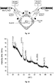
- Figure 2 is an enlargement of the discharge tube 108.
- Figure 3 is a cross-section of the enlargement image of the discharge tube 108.
- the active part of the plasma close to the inner wall of the dielectric tube zones 136 has a high electron density and high ion density. This provides a high capacity of producing excited/active gaseous species. However, the active part of the plasma in the centre of the discharge tube, or central zone 138, is less reactive because of the drop of electron density and lower temperature.
- the substrate 112 is introduced, directed, guided, held and/or maintained in the central zone 138 of the plasma thanks to holding means composing the substrate inlet 102 and the substrate outlet 104.
- the holding means are configured to hold the substrate 112 in a zone corresponding to a region located at the centre of the discharge tube 108, in particular at the centre of the central zone 138.
- the substrate inlet 102 and the substrate outlet 104 in particular the holding means present on said inlet 102 and said outlet 104, prevent the substrate 112 to end up in the filamentary discharge zones 136. This protects the substrates from the high temperature of these zones. This aspect is very valuable when heat-sensitive substrates 112, such as polymers and/or plastics, are to be coated.
- the central zone (138) in which the (heat-sensitive) substrate 112 must be introduced, directed, guided, held and/or maintained is located at a minimal distance of 1 mm from the internal surface of said dielectric tube (108 ; 208).
- the maximum distance from the internal surface of said dielectric tube (108 ; 208) is 2.5 mm.
- the injection of the mist of the metal precursor is performed in the post-discharge region of the electromagnetic surface wave launcher 106 which is at a distance comprises between 0.5 cm and 20 cm from the launching gap 140, preferentially at a distance of 6 cm from the launching gap 140.
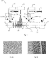
- Figure 4 illustrates the second embodiment of the present invention. This figure 4 shows the numbering of the previous figure 1 for identical or similar elements, however count being incremented by 100. Specific numbers are used for the specific items for this second embodiment.
- the device 200 illustrated on figure 4 is complemented by the fact that it is now possible to generate metallic nanoparticles on the surface of the substrates 212 before the coating with a metal oxide derivative in the post-discharge zone of the device 200.
- the gas source 216 is connected, through the inlet 222, to nanoparticles precursor delivery system 248, preferentially set up in a syringe pump, and similar to the chemical precursor source 218.
- the nanoparticles precursor delivery system 248 is configured to deliver a nanoparticles precursor onto the yet non-activated surface of the substrate 212 through the inlet 222 of the gas source 216.
- Said nanoparticles precursor may be under the form of a mist and/or an aerosol and/or vapour. For this, it may pass through an atomising arrangement 242, preferentially an ultrasonic system, which is located between the nanoparticles precursor delivery system 248 and the plasma gas source 216.
- the ultrasonic system 242 comprises an ultrasonic nozzle 246 adapted for spraying the nanoparticles precursor into a mist and/or an aerosol that will be carried into the plasma gas source 216 and on the yet non-plasma-activated surface of the substrate 212 with carrier gases, such as argon and/or oxygen.
- carrier gases such as argon and/or oxygen.
- the flow of the carrier gas is comprised between 1 and 100 slm, in general of 10 slm and is indicated by the arrows 244.
- the ultrasonic system 242 is working thanks to an ultrasonic generator 250, preferentially an ultrasonic generator from Sono-Tek that operates at 120 kHz.
- metallic nanoparticles are first formed in the gas phase before to cover part of the substrate 212, which is thus coated with a layer of metal oxide derivatives in an identical way that the one describe in the first embodiment of the present invention.
- the device 200 has subsequently two functions: generation of metallic nanoparticles and formation of nanocomposites by subsequent and/or simultaneous deposition of metal oxide derivatives. The arrangement described can be multiplied for the embedment of different nanoparticles.
- Atmospheric pressure plasma enhanced chemical vapour deposition of anatase thin film on PMMA optical fibres at low temperature.
- Titanium ethoxide (Sigma-Aldrich 80%) was used as titanium precursor. It is viscous and poorly volatile at room temperature and in order to control its flow rate with the feeding system 10, it was diluted in hexane (Sigma-Aldrich, ⁇ 97%) to 0.4 M.
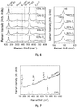
- FIG. 5 shows the SEM images.
- the top view image ( figure 5a ) reveals a homogeneous film with spherical shape particle of a diameter ranging between 30 and 150 nm. Film thickness is about 200 nm.
- the cross section image ( figure 5b ) reveals the homogeneous film of TiO 2 on the polyimide cladding of the silica core of the optical fibres.
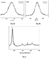
- Figure 6 shows the Raman spectra of TiO 2 thin films grown on Si substrate as function of the oxygen/argon ratio.
- Three well defined Raman peaks at 146 cm -1 , 397 cm -1 and 637 cm -1 are observed for all the films. These peaks correspond to the E g (v6), B 1g (v4) and E g (v1) optical vibration modes and are characteristics of the anatase phase of TiO 2 .
- the strongest E g mode at 146 cm -1 is attributed to the external vibration of the anatase structure.
- the Raman spectra for all samples clearly confirm that the TiO 2 coatings are in pure anatase phase.
- Figure 7 shows the Raman spectra of TiO 2 thin films grown on PMMA polymer optical fibre.
- the well-defined peaks at 146 cm -1 , 397 cm -1 and 637 cm -1 correspond to the E g (v6), B 1g (v4) and E g (v1) optical vibration modes and are characteristics of the anatase phase of TiO 2 .
- the strongest E g mode at 146 cm -1 is attributed to the external vibration of the anatase structure.
- the Raman spectra clearly confirm that the TiO 2 coatings are in pure anatase phase. Peaks observed at 290, 385, 732 and 749 cm -1 are all attributed to the PMMA optical fibre substrate.
- Atmospheric pressure plasma enhanced chemical vapour deposition of boron-doped anatase thin films on silicon wafer substrate at low temperature.
- Titanium ethoxide (Ti(OC 2 H 5 ) 4 , 80%) was diluted in hexane ( ⁇ 97 %) to 0.4 M.
- the titanium precursor flow rate was fixed at 10 ⁇ L ⁇ min -1 and carried toward an ultrasonic nebulizing nozzle operating at 120 kHz (Sono-Tek).
- the drizzle formed at the outlet of the nozzle is composed by droplets with diameters ranging between 10 ⁇ m and 20 ⁇ m and which are carried by a mixture of gases, argon/oxygen, with a flow rate of 0.9 and 1 L ⁇ min -1 respectively.
- the boron precursor i.e.
- boron isopropoxide (B[(CH 3 ) 2 CHO] 3 ), ⁇ 98 %) was placed in a separated bubbler, connected to the nebulizing nozzle, joining simultaneously the flow of Ar (carrier gas).
- the solution was bubbled by using a constant flow of 0.1 L ⁇ min -1 of Ar, making the total flow of Ar carrier gas equal to 1 L ⁇ min -1 (0.9 + 0.1 L ⁇ min -1 ).
- the post-discharge distance from the launching gap was equal to 6 cm after the initiation of the plasma discharge, the deposition was carried out for 10 minutes, keeping constant all the parameters previously described.
- Films were grown on double side polished silicon wafer substrates (2 ⁇ 2 cm). The silicon substrates were cleaned using absolute ethanol (97 %) and dried in air prior to use.
- the substrate was placed in a quartz tube, along with a metallic holder, to avoid the substrate to move during the deposition.
- boron the dopant
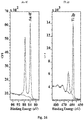
- XPS analyses were performed both on the surface ( figure 8a ) of the film and in depth ( figure 8b ).
- boron the dopant
- B 1s peaks at 190-191 eV are attributed to boron in an oxygen substitutional position and peaks in the range 191-192 eV to interstitial boron.
- Boron can also be found in various other forms, including cationic B 3+ in B 2 O 3 and anionic B 2- in TiB 2 , with a characteristic B 1s peak lying at 193.1 and 187.5 eV, respectively.
- the peak for B 1s in our samples was found at a band energy between 191 and 192 eV (191.35 eV), meaning the dopant, i.e. boron, was incorporated in an interstitial position, is that to say, the film deposited is boron-doped anatase TiO 2 .
- Atmospheric pressure plasma enhanced chemical vapour deposition at low temperature of nanocomposite thin films composed of anatase and preformed silver nanoparticles
- a suspension/solution composed of titanium ethoxide (Sigma-Aldrich, ⁇ 80%) and commercial Ag nanoparticles (Ag NPs) were used to deposit Ag-TiO 2 nanocomposite films.
- the titanium precursor flow rate, controlled by a syringe pump is fixed at 10 ⁇ L/min and carried toward an ultrasonic nebulizing nozzle operating at 120 kHz.
- the discharge was generated at atmospheric pressure inside the quartz discharge tube with a MW power of 200 W and working Ar gas flow of 10 slm.
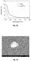
- Figure 11a shows the backscattering SEM images and EDS spectrum of the Ag-TiO 2 composite coating as deposited.
- the top view image reveals a homogeneous film with a presence of Ag spherical shape particles and/or aggregations of nanoparticles.
- the presence of Ag nanoparticles in TiO 2 films was confirmed in EDS spectra ( figure 11b ) with an atomic ratio of 0.07 at. %.
- UV-Vis spectrophotometry was used to compare the optical property of the deposited Ag-TiO 2 composite coating with TiO 2 films. As observed from the spectra in figure 12 , TiO 2 showed an expected strong broad absorption in UV region due to its optical band gap. However, a wide absorption band around 450 nm can be observed in the composite Ag-TiO 2 coating. This significant change is strongly acknowledged to localize surface plasmon resonance delivered by Ag NPs [ K. Awazu et al., J. Am. Chem. Soc., 2008, 130, 1676-1680 ].
- Atmospheric pressure plasma enhanced chemical vapour deposition at low temperature of nanocomposite thin films composed of anatase and in situ synthesized silver nanoparticles.
- Anatase TiO 2 thin films containing silver nanoparticles containing have been deposited using the set up described in figure 4 .
- the liquid silver precursor, nebulized into micrometer-size fine droplets, is subsequently carried to the microwave discharge by mean of a 10 slm flow of Ar carrier gas.
- the microwave power is set up at 200 W.
- the titanium precursor is injected at a flow rate of 10 ⁇ L ⁇ min -1 using a syringe pump and atomized thanks to a Sono-Tek ultrasonic nozzle.
- the titanium precursor droplets are sent to the post discharge zone by means of a carrier gas mixture composed of 1 slm Ar and 1 slm O 2 .
- Anatase TiO 2 thin films containing gold nanoparticles also have been deposited using the set-up described in figure 14 .
- This set-up is based on the one depicted in figure 1 , except that there are two simultaneous injections systems in the post discharge area.
- One provides a first chemical precursor, for example a mist of TiO 2 precursor (for instance, TEOT, titanium (IV) ethoxide) while the other one provides a second chemical precursors, for example a mist of Au precursor (for instance HAuCl 4 .3H 2 O).
- the microwave power is set up at 200 W and the Ar plasma gas flow at 10 slm.
- the titanium precursor (TEOT) is injected at a flow rate of 10 ⁇ L ⁇ min-1 using a syringe pump and atomized thanks to a Sono-Tek ultrasonic nozzle.
- the titanium precursor droplets are sent to the post discharge zone by means of a carrier gas mixture composed of 1 slm Ar and 1 slm O 2 .
- XPS measurements confirms that the coatings are only composed of metallic Au and stoichiometric TiO 2 (only Ti 4+ , no Ti 3+ ) (see figure 16 ).
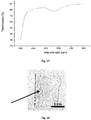
- a plasmonic effect due to Au NPs is observed with a strong absorption in the range 500-600 nm ( figure 17 ). This effect is also observed by naked eyes as the sample exhibits a pink color which is characteristic of Au NPs plasmonic effect ( figure 18 ). The pink color is represented by the shadow area shown by the arrow on figure 18 .
Landscapes
- Chemical & Material Sciences (AREA)
- Engineering & Computer Science (AREA)
- Physics & Mathematics (AREA)
- Plasma & Fusion (AREA)
- Materials Engineering (AREA)
- Mechanical Engineering (AREA)
- Metallurgy (AREA)
- Organic Chemistry (AREA)
- Chemical Kinetics & Catalysis (AREA)
- General Chemical & Material Sciences (AREA)
- Analytical Chemistry (AREA)
- Electromagnetism (AREA)
- Spectroscopy & Molecular Physics (AREA)
- Dispersion Chemistry (AREA)
- Inorganic Chemistry (AREA)
- Chemical Vapour Deposition (AREA)
- Plasma Technology (AREA)
Claims (15)
- Dispositif de dépôt d'une post-décharge par plasma (100 ; 200) pour le dépôt d'un dérivé cristallin d'oxyde métallique sur un substrat (112 ; 212), le dispositif en question comprenant :a) une source de gaz (116 ; 216) qui comprend une entrée (102 ; 202) pour le substrat ;b) une chambre de dépôt de post-décharge (110 ; 210) qui comprend une sortie (104 ; 204) pour le substrat ; ladite entrée (102 ; 202) pour le substrat et ladite sortie (104 ; 204) pour le substrat définissant un axe central longitudinal ;c) un tube diélectrique (108 ; 208) qui est placé entre ladite source de gaz (116; 216) et ladite chambre de dépôt (110; 210) sur ledit axe central longitudinal; ledit tube diélectrique (108 ; 208) étant configuré pour confiner une décharge de plasma ;dans lequel ledit tube diélectrique (108 ; 208) comprend une zone de décharge qui est située sur la surface interne dudit tube diélectrique (108 ; 208) et une zone centrale (138) qui est centrée sur ledit axe central longitudinal ;
ladite zone centrale (138) étant disposée à une distance qui est comprise entre 1 mm et 2,5 mm par rapport à la surface interne dudit tube diélectrique (108 ; 208) ; et dans lequel ledit tube diélectrique (108 ; 208) est entouré par un lanceur d'ondes de surface (106 ; 206) qui est configuré pour générer la décharge de plasma. - Dispositif de dépôt d'une post-décharge par plasma (100 ; 200) selon la revendication 1, dans lequel ledit lanceur d'ondes de surface (106; 206) est configuré pour procurer une température qui est inférieure ou égale à 150 °C dans ladite zone centrale (138), de préférence une température qui est inférieure à 100 °C.
- Dispositif de dépôt d'une post-décharge par plasma (100 ; 200) selon l'une quelconque des revendications 1 à 2, dans lequel ledit tube diélectrique (108; 208) représente un tube de décharge en quartz, en pyrex™, en alumine, en silice ou en n'importe quel matériau diélectrique, de manière préférentielle en quartz.
- Dispositif de dépôt d'une post-décharge par plasma (100 ; 200) selon la revendication 1, dans lequel ledit lanceur d'ondes de surface (106 ; 206) représente un lanceur d'ondes de surface sous la forme de micro-ondes avec une fréquence qui est comprise entre 300 MHz et 300 GHz, de manière préférentielle avec une fréquence de 2,45 GHz.
- Dispositif de dépôt d'une post-décharge par plasma (100 ; 200) selon l'une quelconque des revendications 1 à 4, dans lequel ladite chambre de dépôt de post-décharge (110; 210) est située à une distance qui est comprise entre 0,5 cm et 20 cm par rapport audit lanceur d'ondes de surface (106 ; 206), de manière préférentielle à une distance de 6 cm.
- Dispositif de dépôt d'une post-décharge par plasma (100 ; 200) selon l'une quelconque des revendications 1 à 5, dans lequel ladite source de gaz (116 ; 216) est configurée pour injecter un gaz dans ledit lanceur d'ondes de surface (106; 206), le gaz en question représentant de manière préférentielle de l'argon, de l'hélium, du krypton, du xénon, de l'azote, de l'hydrogène, de l'oxygène et/ou l'une quelconque de leurs combinaisons.
- Dispositif de dépôt d'une post-décharge par plasma (100 ; 200) selon l'une quelconque des revendications 1 à 6, dans lequel le dispositif en question (100 ; 200) comprend en outre une source d'un précurseur de produit chimique (118 ; 218) qui est placée dans la zone de post-décharge du dispositif (100 ; 200) et qui est configurée pour distribuer un précurseur de produit chimique sur la surface d'un substrat (112 ; 122) qui est activée par le plasma, ledit précurseur de produit chimique représentant de manière préférentielle un précurseur d'un dérivé cristallin d'un oxyde métallique, de manière plus préférée un précurseur d'un dérivé cristallin d'un oxyde métallique en mélange avec des nanoparticules métalliques préformées et/ou en mélange avec un précurseur de produit chimique destiné au dopage.
- Dispositif de dépôt d'une post-décharge par plasma (100 ; 200) selon la revendication 7, dans lequel ladite source d'un précurseur de produit chimique (118; 218) est raccordée à un agencement d'atomisation (120; 220) qui est configuré pour distribuer un précurseur de produit chimique sous la forme d'un brouillard et/ou d'un aérosol, ledit agencement d'atomisation (120 ; 220) représentant de manière préférentielle un système à ultrasons.
- Dispositif de dépôt d'une post-décharge par plasma (100 ; 200) selon l'une quelconque des revendications 1 à 8, dans lequel ladite source de gaz (116; 216) comprend en outre un système de distribution d'un précurseur de nanoparticules métalliques (248) qui est configuré pour distribuer un précurseur de nanoparticules métalliques dans ledit gaz, ledit précurseur de nanoparticules métalliques représentant de manière plus préférée un précurseur de nanoparticules d'argent, de palladium, de platine ou d'or.
- Dispositif de dépôt d'une post-décharge par plasma (100 ; 200) selon l'une quelconque des revendications 1 à 9, dans lequel le dispositif en question comprend deux sources de précurseurs de produits chimiques qui sont placées dans la zone de post-décharge du dispositif et qui sont configurées pour distribuer un premier précurseur de produit chimique et un deuxième précurseur de produit chimique sur la surface d'un substrat, activée par plasma, lesdits précurseurs de produits chimiques représentant de manière préférentielle l'éthoxyde de titane(IV) et le trichlorhydrate d'or.
- Procédé de dépôt chimique en phase vapeur amplifié par plasma, comprenant les étapes dans lesquelles :a) on active un substrat (112; 122) dans un dispositif de dépôt d'une post-décharge par plasma dans le but d'obtenir un substrat activé par plasma ;b) on fonctionnalise ledit substrat activé par plasma par l'intermédiaire d'un réactif dans la zone de post-décharge dudit dispositif de dépôt d'une post-décharge par plasma ;caractérisé en ce que ledit dispositif de dépôt d'une post-décharge par plasma représente un dispositif de dépôt d'une post-décharge par plasma (100 ; 200) selon l'une quelconque des revendications 1 à 10.
- Procédé selon la revendication 11, dans lequel ledit dépôt chimique en phase vapeur amplifié par plasma est mis en œuvre sous pression atmosphérique et/ou à une température qui est inférieure ou égale à 150 °C, de préférence à une température qui est inférieure à 100 °C.
- Selon l'une quelconque des revendications 11 à 12, dans lequel ledit substrat (112 ; 212) représente un substrat qui est sensible à la chaleur.
- Selon l'une quelconque des revendications 11 à 13, dans lequel ledit substrat (112 ; 212) représente un substrat unidimensionnel ou un substrat bidimensionnel.
- Selon l'une quelconque des revendications 11 à 14, dans lequel ledit réactif représente un dérivé cristallin d'un oxyde métallique, de manière préférentielle du TiO2, du ZnO, du WO3, ou un dérivé cristallin dopé d'un oxyde métallique, de manière préférentielle du TiO2 qui est dopé avec du bore, ou un mélange de nanoparticules métalliques avec un dérivé cristallin d'un oxyde métallique.
Priority Applications (1)
| Application Number | Priority Date | Filing Date | Title |
|---|---|---|---|
| PL17768110T PL3513423T3 (pl) | 2016-09-15 | 2017-09-14 | Urządzenie i sposób do przeprowadzania chemicznego osadzania z fazy gazowej wspomaganego plazmą pod ciśnieniem atmosferycznym w niskiej temperaturze |
Applications Claiming Priority (2)
| Application Number | Priority Date | Filing Date | Title |
|---|---|---|---|
| LU93221A LU93221B1 (en) | 2016-09-15 | 2016-09-15 | Device for performing atmospheric pressure plasma enhanced chemical vapour deposition at low temperature |
| PCT/EP2017/073165 WO2018050758A1 (fr) | 2016-09-15 | 2017-09-14 | Dispositif pour réaliser un dépôt chimique en phase vapeur assisté par plasma à pression atmosphérique à basse température |
Publications (2)
| Publication Number | Publication Date |
|---|---|
| EP3513423A1 EP3513423A1 (fr) | 2019-07-24 |
| EP3513423B1 true EP3513423B1 (fr) | 2020-11-18 |
Family
ID=57178453
Family Applications (1)
| Application Number | Title | Priority Date | Filing Date |
|---|---|---|---|
| EP17768110.3A Active EP3513423B1 (fr) | 2016-09-15 | 2017-09-14 | Dispositif et méthode pour réaliser un dépôt chimique en phase vapeur assisté par plasma à pression atmosphérique à basse température |
Country Status (7)
| Country | Link |
|---|---|
| US (1) | US20190259583A1 (fr) |
| EP (1) | EP3513423B1 (fr) |
| JP (1) | JP7253255B2 (fr) |
| ES (1) | ES2854982T3 (fr) |
| LU (1) | LU93221B1 (fr) |
| PL (1) | PL3513423T3 (fr) |
| WO (1) | WO2018050758A1 (fr) |
Families Citing this family (2)
| Publication number | Priority date | Publication date | Assignee | Title |
|---|---|---|---|---|
| US11251430B2 (en) | 2018-03-05 | 2022-02-15 | The Research Foundation For The State University Of New York | ϵ-VOPO4 cathode for lithium ion batteries |
| TWI754245B (zh) * | 2020-03-17 | 2022-02-01 | 國立陽明交通大學 | 電漿系統及混合電漿與水霧的方法 |
Family Cites Families (8)
| Publication number | Priority date | Publication date | Assignee | Title |
|---|---|---|---|---|
| FR2664294B1 (fr) * | 1990-07-06 | 1992-10-23 | Plasmametal | Procede de metallisation d'une surface. |
| JP3206095B2 (ja) * | 1991-04-12 | 2001-09-04 | 株式会社ブリヂストン | 表面処理方法及びその装置 |
| FR2872068B1 (fr) * | 2004-06-28 | 2006-10-27 | Centre Nat Rech Scient Cnrse | Procede et dispositif pour le depot de couches minces par pulverisation electrohydrodynamique, notamment en post-decharge |
| JP2006324146A (ja) * | 2005-05-19 | 2006-11-30 | Shimada Phys & Chem Ind Co Ltd | 大気圧マイクロ波プラズマ反応装置および方法 |
| US20070212486A1 (en) * | 2005-05-20 | 2007-09-13 | Dinega Dmitry P | Plasma Enhanced Chemical Vapor Deposition of Metal Oxide |
| JP4862193B2 (ja) * | 2006-07-24 | 2012-01-25 | 古河電気工業株式会社 | 半導体膜形成装置、半導体膜形成方法、及び半導体膜付き線条体 |
| JP2008073986A (ja) * | 2006-09-22 | 2008-04-03 | Dainippon Printing Co Ltd | ガスバリア性積層フィルム |
| EP2354272B1 (fr) * | 2010-02-08 | 2016-08-24 | Graphene Square Inc. | Appareil pour le revêtement de la surface interne et externe d'un tube enroulé en continu et procédé de revêtement avec du graphène utilisant cet appareil |
-
2016
- 2016-09-15 LU LU93221A patent/LU93221B1/en active IP Right Grant
-
2017
- 2017-09-14 US US16/333,819 patent/US20190259583A1/en not_active Abandoned
- 2017-09-14 ES ES17768110T patent/ES2854982T3/es active Active
- 2017-09-14 PL PL17768110T patent/PL3513423T3/pl unknown
- 2017-09-14 EP EP17768110.3A patent/EP3513423B1/fr active Active
- 2017-09-14 JP JP2019512614A patent/JP7253255B2/ja active Active
- 2017-09-14 WO PCT/EP2017/073165 patent/WO2018050758A1/fr not_active Ceased
Non-Patent Citations (1)
| Title |
|---|
| None * |
Also Published As
| Publication number | Publication date |
|---|---|
| PL3513423T3 (pl) | 2021-07-19 |
| LU93221B1 (en) | 2018-04-11 |
| EP3513423A1 (fr) | 2019-07-24 |
| WO2018050758A1 (fr) | 2018-03-22 |
| JP7253255B2 (ja) | 2023-04-06 |
| ES2854982T3 (es) | 2021-09-23 |
| JP2019533078A (ja) | 2019-11-14 |
| US20190259583A1 (en) | 2019-08-22 |
Similar Documents
| Publication | Publication Date | Title |
|---|---|---|
| US12024635B2 (en) | Carbon-nanotube-based composite coating and production method thereof | |
| US20160289826A1 (en) | Method for continuous production of aligned nanostructures on a running substrate and related device | |
| Quesada-González et al. | Interstitial boron-doped anatase TiO 2 thin-films on optical fibres: atmospheric pressure-plasma enhanced chemical vapour deposition as the key for functional oxide coatings on temperature-sensitive substrates | |
| Ussenov et al. | Particle formation during deposition of SiO x nanostructured thin films by atmospheric pressure plasma jet | |
| Kusdianto et al. | Fabrication and application of ZnO-Ag nanocomposite materials prepared by gas-phase methods | |
| EP3513423B1 (fr) | Dispositif et méthode pour réaliser un dépôt chimique en phase vapeur assisté par plasma à pression atmosphérique à basse température | |
| Yuan et al. | The synthesis of C, N-codoped TiO2 hollow spheres by a dual-frequency atmospheric pressure cold plasma jet | |
| JP2016537291A (ja) | 液体シランを使用したSiベースナノ材料の合成 | |
| Seo et al. | Enhanced photocatalytic properties of nanoclustered P-doped TiO2 films deposited by advanced atmospheric plasma jet | |
| EP3490937B1 (fr) | Procédé de préparation de nanocomposites | |
| Duminica et al. | Pyrosol deposition of anatase TiO2 thin films starting from Ti (OiPr) 4/acetylacetone solutions | |
| DE102017216139B3 (de) | Verfahren zur Herstellung einer Schicht | |
| EP3655563B1 (fr) | Dispositif à plasma destiné à déposer un film composite fonctionnel comprenant des particules cristallisées intégrées dans une matrice, et procédé de dépôt correspondant | |
| Beaudette | Nanostructures, nanoparticles, and 2D materials from nonthermal plasmas | |
| JP6717663B2 (ja) | 膜形成方法 | |
| Bizeray et al. | Preparation and Characterization of Nanocomposite Thin Films Containing Gold Nanoparticles by a Single-Step Atmospheric Pressure Plasma Deposition Process | |
| Shujah et al. | Effect of deposition temperature variation on thin films synthesis via AACVD | |
| Bizeray et al. | Nanocomposite layers synthesized by atmospheric-pressure plasma combined with an aerosolized gold salt solution: influence of the solution concentration | |
| Witanachchi et al. | Laser-assisted spray pyrolysis process for the growth of TiO2 and Fe2O3 nanoparticle coatings | |
| EP3680361A1 (fr) | Embout de dosage d'un précurseur et procédé de fabrication d'une couche | |
| Simfroso et al. | Solution Precursor Plasma Spraying of TiO2 Coatings Using a Catalyst-Free Precursor. Materials 2023, 16, 1515 | |
| Korotcenkov et al. | Synthesis and deposition of sensor materials | |
| Wang et al. | Highly Active Ag-TiO2 Nanocomposite from Atom Deposition in Ethylenediamine-Complexing Silver Mirror Reaction | |
| Pourali et al. | Atmospheric-Pressure PECVD of SnO2 Thin Films in a Dielectric Barrier Discharge Reactor: Influence of Deposition Strategy and Substrate on Film Structure and Morphology | |
| Quesada-Gonzalez | Synthesis and characterisation of B-TiO₂ thin films by atmospheric pressure chemical vapour deposition and plasma enhanced chemical vapour deposition: functional films for different substrates |
Legal Events
| Date | Code | Title | Description |
|---|---|---|---|
| STAA | Information on the status of an ep patent application or granted ep patent |
Free format text: STATUS: UNKNOWN |
|
| STAA | Information on the status of an ep patent application or granted ep patent |
Free format text: STATUS: THE INTERNATIONAL PUBLICATION HAS BEEN MADE |
|
| PUAI | Public reference made under article 153(3) epc to a published international application that has entered the european phase |
Free format text: ORIGINAL CODE: 0009012 |
|
| STAA | Information on the status of an ep patent application or granted ep patent |
Free format text: STATUS: REQUEST FOR EXAMINATION WAS MADE |
|
| 17P | Request for examination filed |
Effective date: 20190304 |
|
| AK | Designated contracting states |
Kind code of ref document: A1 Designated state(s): AL AT BE BG CH CY CZ DE DK EE ES FI FR GB GR HR HU IE IS IT LI LT LU LV MC MK MT NL NO PL PT RO RS SE SI SK SM TR |
|
| AX | Request for extension of the european patent |
Extension state: BA ME |
|
| DAV | Request for validation of the european patent (deleted) | ||
| DAX | Request for extension of the european patent (deleted) | ||
| GRAP | Despatch of communication of intention to grant a patent |
Free format text: ORIGINAL CODE: EPIDOSNIGR1 |
|
| STAA | Information on the status of an ep patent application or granted ep patent |
Free format text: STATUS: GRANT OF PATENT IS INTENDED |
|
| INTG | Intention to grant announced |
Effective date: 20200527 |
|
| GRAS | Grant fee paid |
Free format text: ORIGINAL CODE: EPIDOSNIGR3 |
|
| GRAA | (expected) grant |
Free format text: ORIGINAL CODE: 0009210 |
|
| STAA | Information on the status of an ep patent application or granted ep patent |
Free format text: STATUS: THE PATENT HAS BEEN GRANTED |
|
| AK | Designated contracting states |
Kind code of ref document: B1 Designated state(s): AL AT BE BG CH CY CZ DE DK EE ES FI FR GB GR HR HU IE IS IT LI LT LU LV MC MK MT NL NO PL PT RO RS SE SI SK SM TR |
|
| REG | Reference to a national code |
Ref country code: GB Ref legal event code: FG4D |
|
| REG | Reference to a national code |
Ref country code: CH Ref legal event code: EP |
|
| REG | Reference to a national code |
Ref country code: IE Ref legal event code: FG4D |
|
| REG | Reference to a national code |
Ref country code: DE Ref legal event code: R096 Ref document number: 602017027858 Country of ref document: DE |
|
| REG | Reference to a national code |
Ref country code: AT Ref legal event code: REF Ref document number: 1336678 Country of ref document: AT Kind code of ref document: T Effective date: 20201215 |
|
| REG | Reference to a national code |
Ref country code: FI Ref legal event code: FGE |
|
| REG | Reference to a national code |
Ref country code: CH Ref legal event code: NV Representative=s name: DR. ALEXANDER MILLER, LL.M., CH |
|
| REG | Reference to a national code |
Ref country code: SE Ref legal event code: TRGR |
|
| REG | Reference to a national code |
Ref country code: NL Ref legal event code: FP |
|
| REG | Reference to a national code |
Ref country code: SK Ref legal event code: T3 Ref document number: E 36602 Country of ref document: SK |
|
| PG25 | Lapsed in a contracting state [announced via postgrant information from national office to epo] |
Ref country code: GR Free format text: LAPSE BECAUSE OF FAILURE TO SUBMIT A TRANSLATION OF THE DESCRIPTION OR TO PAY THE FEE WITHIN THE PRESCRIBED TIME-LIMIT Effective date: 20210219 Ref country code: PT Free format text: LAPSE BECAUSE OF FAILURE TO SUBMIT A TRANSLATION OF THE DESCRIPTION OR TO PAY THE FEE WITHIN THE PRESCRIBED TIME-LIMIT Effective date: 20210318 Ref country code: RS Free format text: LAPSE BECAUSE OF FAILURE TO SUBMIT A TRANSLATION OF THE DESCRIPTION OR TO PAY THE FEE WITHIN THE PRESCRIBED TIME-LIMIT Effective date: 20201118 |
|
| REG | Reference to a national code |
Ref country code: NO Ref legal event code: T2 Effective date: 20201118 |
|
| PG25 | Lapsed in a contracting state [announced via postgrant information from national office to epo] |
Ref country code: IS Free format text: LAPSE BECAUSE OF FAILURE TO SUBMIT A TRANSLATION OF THE DESCRIPTION OR TO PAY THE FEE WITHIN THE PRESCRIBED TIME-LIMIT Effective date: 20210318 Ref country code: LV Free format text: LAPSE BECAUSE OF FAILURE TO SUBMIT A TRANSLATION OF THE DESCRIPTION OR TO PAY THE FEE WITHIN THE PRESCRIBED TIME-LIMIT Effective date: 20201118 Ref country code: BG Free format text: LAPSE BECAUSE OF FAILURE TO SUBMIT A TRANSLATION OF THE DESCRIPTION OR TO PAY THE FEE WITHIN THE PRESCRIBED TIME-LIMIT Effective date: 20210218 |
|
| REG | Reference to a national code |
Ref country code: LT Ref legal event code: MG9D |
|
| PG25 | Lapsed in a contracting state [announced via postgrant information from national office to epo] |
Ref country code: HR Free format text: LAPSE BECAUSE OF FAILURE TO SUBMIT A TRANSLATION OF THE DESCRIPTION OR TO PAY THE FEE WITHIN THE PRESCRIBED TIME-LIMIT Effective date: 20201118 |
|
| PG25 | Lapsed in a contracting state [announced via postgrant information from national office to epo] |
Ref country code: SM Free format text: LAPSE BECAUSE OF FAILURE TO SUBMIT A TRANSLATION OF THE DESCRIPTION OR TO PAY THE FEE WITHIN THE PRESCRIBED TIME-LIMIT Effective date: 20201118 Ref country code: LT Free format text: LAPSE BECAUSE OF FAILURE TO SUBMIT A TRANSLATION OF THE DESCRIPTION OR TO PAY THE FEE WITHIN THE PRESCRIBED TIME-LIMIT Effective date: 20201118 Ref country code: EE Free format text: LAPSE BECAUSE OF FAILURE TO SUBMIT A TRANSLATION OF THE DESCRIPTION OR TO PAY THE FEE WITHIN THE PRESCRIBED TIME-LIMIT Effective date: 20201118 Ref country code: RO Free format text: LAPSE BECAUSE OF FAILURE TO SUBMIT A TRANSLATION OF THE DESCRIPTION OR TO PAY THE FEE WITHIN THE PRESCRIBED TIME-LIMIT Effective date: 20201118 |
|
| REG | Reference to a national code |
Ref country code: DE Ref legal event code: R097 Ref document number: 602017027858 Country of ref document: DE |
|
| PG25 | Lapsed in a contracting state [announced via postgrant information from national office to epo] |
Ref country code: DK Free format text: LAPSE BECAUSE OF FAILURE TO SUBMIT A TRANSLATION OF THE DESCRIPTION OR TO PAY THE FEE WITHIN THE PRESCRIBED TIME-LIMIT Effective date: 20201118 |
|
| REG | Reference to a national code |
Ref country code: ES Ref legal event code: FG2A Ref document number: 2854982 Country of ref document: ES Kind code of ref document: T3 Effective date: 20210923 |
|
| PLBE | No opposition filed within time limit |
Free format text: ORIGINAL CODE: 0009261 |
|
| STAA | Information on the status of an ep patent application or granted ep patent |
Free format text: STATUS: NO OPPOSITION FILED WITHIN TIME LIMIT |
|
| 26N | No opposition filed |
Effective date: 20210819 |
|
| PG25 | Lapsed in a contracting state [announced via postgrant information from national office to epo] |
Ref country code: AL Free format text: LAPSE BECAUSE OF FAILURE TO SUBMIT A TRANSLATION OF THE DESCRIPTION OR TO PAY THE FEE WITHIN THE PRESCRIBED TIME-LIMIT Effective date: 20201118 |
|
| PG25 | Lapsed in a contracting state [announced via postgrant information from national office to epo] |
Ref country code: SI Free format text: LAPSE BECAUSE OF FAILURE TO SUBMIT A TRANSLATION OF THE DESCRIPTION OR TO PAY THE FEE WITHIN THE PRESCRIBED TIME-LIMIT Effective date: 20201118 |
|
| GBPC | Gb: european patent ceased through non-payment of renewal fee |
Effective date: 20210914 |
|
| PG25 | Lapsed in a contracting state [announced via postgrant information from national office to epo] |
Ref country code: IS Free format text: LAPSE BECAUSE OF FAILURE TO SUBMIT A TRANSLATION OF THE DESCRIPTION OR TO PAY THE FEE WITHIN THE PRESCRIBED TIME-LIMIT Effective date: 20210318 Ref country code: MC Free format text: LAPSE BECAUSE OF FAILURE TO SUBMIT A TRANSLATION OF THE DESCRIPTION OR TO PAY THE FEE WITHIN THE PRESCRIBED TIME-LIMIT Effective date: 20201118 |
|
| PG25 | Lapsed in a contracting state [announced via postgrant information from national office to epo] |
Ref country code: IE Free format text: LAPSE BECAUSE OF NON-PAYMENT OF DUE FEES Effective date: 20210914 Ref country code: GB Free format text: LAPSE BECAUSE OF NON-PAYMENT OF DUE FEES Effective date: 20210914 |
|
| PG25 | Lapsed in a contracting state [announced via postgrant information from national office to epo] |
Ref country code: CY Free format text: LAPSE BECAUSE OF FAILURE TO SUBMIT A TRANSLATION OF THE DESCRIPTION OR TO PAY THE FEE WITHIN THE PRESCRIBED TIME-LIMIT Effective date: 20201118 |
|
| PG25 | Lapsed in a contracting state [announced via postgrant information from national office to epo] |
Ref country code: HU Free format text: LAPSE BECAUSE OF FAILURE TO SUBMIT A TRANSLATION OF THE DESCRIPTION OR TO PAY THE FEE WITHIN THE PRESCRIBED TIME-LIMIT; INVALID AB INITIO Effective date: 20170914 |
|
| PGFP | Annual fee paid to national office [announced via postgrant information from national office to epo] |
Ref country code: NO Payment date: 20230830 Year of fee payment: 7 Ref country code: IT Payment date: 20230925 Year of fee payment: 7 Ref country code: FI Payment date: 20230925 Year of fee payment: 7 Ref country code: CZ Payment date: 20230908 Year of fee payment: 7 Ref country code: AT Payment date: 20230925 Year of fee payment: 7 |
|
| PGFP | Annual fee paid to national office [announced via postgrant information from national office to epo] |
Ref country code: SK Payment date: 20230907 Year of fee payment: 7 Ref country code: SE Payment date: 20230830 Year of fee payment: 7 Ref country code: PL Payment date: 20230818 Year of fee payment: 7 Ref country code: NL Payment date: 20230925 Year of fee payment: 7 Ref country code: BE Payment date: 20230928 Year of fee payment: 7 |
|
| PGFP | Annual fee paid to national office [announced via postgrant information from national office to epo] |
Ref country code: ES Payment date: 20231004 Year of fee payment: 7 |
|
| PGFP | Annual fee paid to national office [announced via postgrant information from national office to epo] |
Ref country code: CH Payment date: 20231001 Year of fee payment: 7 |
|
| PG25 | Lapsed in a contracting state [announced via postgrant information from national office to epo] |
Ref country code: MK Free format text: LAPSE BECAUSE OF FAILURE TO SUBMIT A TRANSLATION OF THE DESCRIPTION OR TO PAY THE FEE WITHIN THE PRESCRIBED TIME-LIMIT Effective date: 20201118 |
|
| PG25 | Lapsed in a contracting state [announced via postgrant information from national office to epo] |
Ref country code: TR Free format text: LAPSE BECAUSE OF FAILURE TO SUBMIT A TRANSLATION OF THE DESCRIPTION OR TO PAY THE FEE WITHIN THE PRESCRIBED TIME-LIMIT Effective date: 20201118 |
|
| PG25 | Lapsed in a contracting state [announced via postgrant information from national office to epo] |
Ref country code: MT Free format text: LAPSE BECAUSE OF FAILURE TO SUBMIT A TRANSLATION OF THE DESCRIPTION OR TO PAY THE FEE WITHIN THE PRESCRIBED TIME-LIMIT Effective date: 20201118 |
|
| PG25 | Lapsed in a contracting state [announced via postgrant information from national office to epo] |
Ref country code: FI Free format text: LAPSE BECAUSE OF NON-PAYMENT OF DUE FEES Effective date: 20240914 |
|
| PG25 | Lapsed in a contracting state [announced via postgrant information from national office to epo] |
Ref country code: CZ Free format text: LAPSE BECAUSE OF NON-PAYMENT OF DUE FEES Effective date: 20240914 |
|
| REG | Reference to a national code |
Ref country code: SE Ref legal event code: EUG |
|
| REG | Reference to a national code |
Ref country code: CH Ref legal event code: PL |
|
| REG | Reference to a national code |
Ref country code: NL Ref legal event code: MM Effective date: 20241001 Ref country code: SK Ref legal event code: MM4A Ref document number: E 36602 Country of ref document: SK Effective date: 20240914 |
|
| REG | Reference to a national code |
Ref country code: AT Ref legal event code: MM01 Ref document number: 1336678 Country of ref document: AT Kind code of ref document: T Effective date: 20240914 |
|
| PG25 | Lapsed in a contracting state [announced via postgrant information from national office to epo] |
Ref country code: NL Free format text: LAPSE BECAUSE OF NON-PAYMENT OF DUE FEES Effective date: 20241001 |
|
| REG | Reference to a national code |
Ref country code: BE Ref legal event code: MM Effective date: 20240930 |
|
| PG25 | Lapsed in a contracting state [announced via postgrant information from national office to epo] |
Ref country code: NO Free format text: LAPSE BECAUSE OF NON-PAYMENT OF DUE FEES Effective date: 20240930 |
|
| PG25 | Lapsed in a contracting state [announced via postgrant information from national office to epo] |
Ref country code: IT Free format text: LAPSE BECAUSE OF NON-PAYMENT OF DUE FEES Effective date: 20240914 Ref country code: BE Free format text: LAPSE BECAUSE OF NON-PAYMENT OF DUE FEES Effective date: 20240930 |
|
| REG | Reference to a national code |
Ref country code: AT Ref legal event code: UEP Ref document number: 1336678 Country of ref document: AT Kind code of ref document: T Effective date: 20201118 |
|
| PG25 | Lapsed in a contracting state [announced via postgrant information from national office to epo] |
Ref country code: CH Free format text: LAPSE BECAUSE OF NON-PAYMENT OF DUE FEES Effective date: 20240930 |
|
| PG25 | Lapsed in a contracting state [announced via postgrant information from national office to epo] |
Ref country code: AT Free format text: LAPSE BECAUSE OF NON-PAYMENT OF DUE FEES Effective date: 20240914 |
|
| PG25 | Lapsed in a contracting state [announced via postgrant information from national office to epo] |
Ref country code: SK Free format text: LAPSE BECAUSE OF NON-PAYMENT OF DUE FEES Effective date: 20240914 |
|
| PGFP | Annual fee paid to national office [announced via postgrant information from national office to epo] |
Ref country code: DE Payment date: 20250929 Year of fee payment: 9 |
|
| PG25 | Lapsed in a contracting state [announced via postgrant information from national office to epo] |
Ref country code: SE Free format text: LAPSE BECAUSE OF NON-PAYMENT OF DUE FEES Effective date: 20240915 |
|
| PGFP | Annual fee paid to national office [announced via postgrant information from national office to epo] |
Ref country code: LU Payment date: 20250929 Year of fee payment: 9 |
|
| PGFP | Annual fee paid to national office [announced via postgrant information from national office to epo] |
Ref country code: FR Payment date: 20250925 Year of fee payment: 9 |
|
| REG | Reference to a national code |
Ref country code: ES Ref legal event code: FD2A Effective date: 20251031 |
|
| PG25 | Lapsed in a contracting state [announced via postgrant information from national office to epo] |
Ref country code: PL Free format text: LAPSE BECAUSE OF NON-PAYMENT OF DUE FEES Effective date: 20240914 |
|
| PG25 | Lapsed in a contracting state [announced via postgrant information from national office to epo] |
Ref country code: ES Free format text: LAPSE BECAUSE OF NON-PAYMENT OF DUE FEES Effective date: 20240915 |