EP3513425B1 - Verfahren zur herstellung einer kristallinen siliziumschicht und siliziumbasiertes halbleiterbauelement - Google Patents
Verfahren zur herstellung einer kristallinen siliziumschicht und siliziumbasiertes halbleiterbauelement Download PDFInfo
- Publication number
- EP3513425B1 EP3513425B1 EP17771694.1A EP17771694A EP3513425B1 EP 3513425 B1 EP3513425 B1 EP 3513425B1 EP 17771694 A EP17771694 A EP 17771694A EP 3513425 B1 EP3513425 B1 EP 3513425B1
- Authority
- EP
- European Patent Office
- Prior art keywords
- oxide
- reducing agent
- crystalline silicon
- silicon layer
- substrate
- Prior art date
- Legal status (The legal status is an assumption and is not a legal conclusion. Google has not performed a legal analysis and makes no representation as to the accuracy of the status listed.)
- Active
Links
Images
Classifications
-
- H—ELECTRICITY
- H10—SEMICONDUCTOR DEVICES; ELECTRIC SOLID-STATE DEVICES NOT OTHERWISE PROVIDED FOR
- H10P—GENERIC PROCESSES OR APPARATUS FOR THE MANUFACTURE OR TREATMENT OF DEVICES COVERED BY CLASS H10
- H10P14/00—Formation of materials, e.g. in the shape of layers or pillars
- H10P14/20—Formation of materials, e.g. in the shape of layers or pillars of semiconductor materials
-
- C—CHEMISTRY; METALLURGY
- C01—INORGANIC CHEMISTRY
- C01B—NON-METALLIC ELEMENTS; COMPOUNDS THEREOF; METALLOIDS OR COMPOUNDS THEREOF NOT COVERED BY SUBCLASS C01C
- C01B33/00—Silicon; Compounds thereof
- C01B33/02—Silicon
- C01B33/021—Preparation
- C01B33/023—Preparation by reduction of silica or free silica-containing material
-
- H—ELECTRICITY
- H10—SEMICONDUCTOR DEVICES; ELECTRIC SOLID-STATE DEVICES NOT OTHERWISE PROVIDED FOR
- H10P—GENERIC PROCESSES OR APPARATUS FOR THE MANUFACTURE OR TREATMENT OF DEVICES COVERED BY CLASS H10
- H10P14/00—Formation of materials, e.g. in the shape of layers or pillars
- H10P14/20—Formation of materials, e.g. in the shape of layers or pillars of semiconductor materials
- H10P14/29—Formation of materials, e.g. in the shape of layers or pillars of semiconductor materials characterised by the substrates
- H10P14/2901—Materials
- H10P14/2922—Materials being non-crystalline insulating materials, e.g. glass or polymers
-
- H—ELECTRICITY
- H10—SEMICONDUCTOR DEVICES; ELECTRIC SOLID-STATE DEVICES NOT OTHERWISE PROVIDED FOR
- H10P—GENERIC PROCESSES OR APPARATUS FOR THE MANUFACTURE OR TREATMENT OF DEVICES COVERED BY CLASS H10
- H10P14/00—Formation of materials, e.g. in the shape of layers or pillars
- H10P14/20—Formation of materials, e.g. in the shape of layers or pillars of semiconductor materials
- H10P14/34—Deposited materials, e.g. layers
- H10P14/3402—Deposited materials, e.g. layers characterised by the chemical composition
- H10P14/3404—Deposited materials, e.g. layers characterised by the chemical composition being Group IVA materials
- H10P14/3411—Silicon, silicon germanium or germanium
Definitions
- the invention relates to a method for producing a crystalline silicon layer on the surface of a substrate containing SiO 2 .
- the invention also relates to a silicon-based semiconductor component that is produced using such a method.
- the invention has the advantage that any SiO 2 -containing substrates can be converted into components with a crystalline silicon layer in mass production using simple means.
- Any SiO 2 -containing substrates can be used, for example islands, partial areas, ingredients or just surfaces of a carrier material.
- the substrate or carrier material can also be flexible films.
- the SiO 2 -containing substrate or its surface can also be structured.
- substrates in the form of float glass panes or other quartz glass substrates can be used, which are correspondingly inexpensive be converted and used after the conversion as a silicon-based semiconductor component.
- the SiO 2 -containing substrate can be provided in particular in the form of a flat or planar plate, for example in the form of a glass plate. Apart from negligible impurities, the SiO 2 -containing substrate can consist of pure SiO 2 .
- a further advantage of the invention is that the simple production steps explained can be used to provide a silicon layer with a high level of purity, which is already suitable for applications in photovoltaics or for other semiconductor components even without subsequent further processing steps.
- the desired crystalline structure of the silicon is immediately provided, which also has a firm connection to the substrate.
- the oxide-containing reducing agent can be any oxide-containing metallic material that is suitable for converting SiO 2 to crystalline silicon in a reduction reaction.
- the reducing agent can have an oxidized surface, for example, with which it is applied directly or via the at least one intermediate layer to the surface of the substrate to be provided with the crystalline silicon layer.
- the oxide-containing reductant is an oxide-containing metal reductant, such as an oxidized metal reductant.
- the oxide-containing metallic reducing agent can be any metal or metal-like substance capable of converting SiO 2 to crystalline silicon in a reduction reaction.
- Aluminum, magnesium, potassium, for example, are suitable, in particular in the form of alkaline earth metal.
- the oxide-containing reducing agent can be used in different consistencies, for example in pasty form, such as screen printing paste, or in solid form, for example as a film.
- Capacitor foil for example, has proven to be particularly suitable. Due to its surface roughness, this has a particularly large Surface, so that a particularly well-defined metal oxide layer is formed on the surface.
- an oxide-containing reducing agent is used in pasty form, such as screen printing paste
- this paste can also be used to dope the silicon of the crystalline silicon layer produced, for example p-doping using aluminum. Electrical conductor tracks can also be produced on the surface of the silicon layer will.
- Another advantage of such a pasty reducing agent is that it retains its position and does not flow.
- a structured silicon layer can be produced by means of the oxide-containing reducing agent in paste form, for example by applying the paste-like reducing agent to the substrate via a mask containing the corresponding structuring and accordingly by the reduction reaction only at certain points where the paste is located , the conversion of the SiO 2 is carried out in crystalline silicon.
- p-doping of the silicon is produced, for example, by means of aluminum and n-doping, for example, by means of magnesium as a reducing agent.
- the oxide-containing reducing agent can also be applied to the substrate in a gaseous phase, for example by a vapor deposition process.
- a vapor deposition process it is advantageous for the production of a high-purity crystalline silicon layer, for example, if the reducing agent containing oxide is vapour-deposited in several individual steps and a venting is carried out in the vapor-deposition chamber of the vapor-deposition system between these steps. In this way, the metal oxide layer just evaporated is oxidized. By repeating this process several times, thin metal oxide layers can be produced, which form a good basis for the subsequent conversion of the SiO 2 into crystalline silicon.
- the oxide-containing reducing agent can be vapor deposited for a longer period of time in order to produce a thicker final layer of this material.
- a structured formation of the crystalline silicon layer can also be produced in that the oxide-containing reducing agent is vapour-deposited via a mask which contains the corresponding structuring.
- a doping material can be added during the vapor deposition process in order to provide the resulting silicon layer with doping.
- the application of the oxide-containing reducing agent according to step b) can also be carried out by rolling, e.g. by the oxide-containing reducing agent being rolled onto the substrate or the intermediate layer with the oxidized surface under pressure and possibly with heating.
- the crystalline silicon layer can then be produced in accordance with step c).
- the heating or the process temperature achieved as a result can be increased from step b) to step c).
- the crystalline silicon layer can also be structured by pressing the oxide-containing reducing agent onto the substrate using a structured pressure plate, ie a pressure plate which has elevations and depressions corresponding to the desired structure of the silicon layer.
- the pressure plate has an elevation at those points at which the SiO 2 is to be converted into crystalline silicon, so that pressure is exerted on the oxide-containing reducing agent at these points.
- no corresponding contact pressure is exerted on the oxide-containing reducing agent, so that there is no conversion of the SiO 2 into crystalline silicon underneath either.
- the crystalline silicon layer can also be structured by local laser heating.
- the oxide-containing reducing agent with or without its oxidized surface can also initially be prepared on a component other than the substrate, for example on a foil. From this other component, the oxide-containing reducing agent prepared in this way with the oxidized surface can then be applied to the Substrate are transferred, for example by pressing, in particular with simultaneous heating of the arrangement.
- the layer or layers to be applied to the surface of the substrate to be provided with the crystalline silicon layer can also be applied by means of galvanic and/or electrochemical processes, e.g. by anodizing.
- the total duration of the process until the crystalline silicon layer is produced in the desired manner can range from 30 minutes to five hours.
- the pressing takes place with an initially high pressing pressure, which is reduced in the further course of the pressing process.
- the reduction of the pressing pressure from the initially high value can take place, for example, in one or more stages and/or with smooth transitions, e.g. after a decay function.
- the initially high compaction pressure can be maintained for a short period of time, for example for a period of up to half an hour, and thereafter a reduced compaction pressure for a period of for example one to three hours.
- the pressing pressure in particular the initially high pressing pressure, can be in the range of ⁇ 1.5 MPa, or ⁇ 1 MPa, ie at relatively low values. Such pressing pressure values can also be generated with simple devices and systems. Depending on how the process is carried out, the required minimum pressing pressure can be specified, e.g. at a minimum value of 20 kPa or 50 kPa.
- the process temperature is below the melting temperature of the metallic reducing agent.
- a low-temperature manufacturing process for the crystalline silicon layer the surface of the SiO 2 -containing substrate are provided.
- no heating processes to extremely high process temperatures are required; for example, temperatures in the range of 600° C. are sufficient if aluminum is used as the reducing agent.
- the process temperature is in the range of +/-50° C. in the range of the glass transition temperature of the substrate. This also allows a favorable, relatively low temperature range to be used for the process temperature. If the glass transition temperature of the SiO 2 -containing substrate is, for example, in the range from 600° C. to 630° C., the process temperature can be set slightly lower, for example at 590° C. In general, the process temperature can then be set in the range from 550°C to 680°C.
- the crystalline silicon layer is produced as a thin layer with a maximum layer thickness of 100 ⁇ m, in particular a maximum of 50 ⁇ m.
- a maximum layer thickness of 100 ⁇ m in particular a maximum of 50 ⁇ m.
- the crystalline silicon layer is produced with grain sizes in the range from nanocrystalline to multicrystalline.
- a constructive starting material can be provided, for example, for building-integrated photovoltaics, TFT displays or other semiconductor components.
- the method is carried out without a vacuum and without an inert gas. Accordingly, the method can be carried out with simple means, in particular with inexpensive devices and systems.
- a layer of a further oxide-containing reducing agent is arranged and then the production of the crystalline silicon layer is carried out.
- the conversion process of the SiO 2 of the substrate into the crystalline silicon layer can be further optimized by the intermediate layer.
- the intermediate layer can also have or consist of an already oxidized material.
- a layer of a further metallic reducing agent can be arranged as an intermediate layer between the oxide layer of the metallic reducing agent and the surface of the substrate to be provided with the crystalline silicon layer, and the crystalline silicon layer can then be produced.
- the further oxide-containing reducing agent is the same as the first-mentioned oxide-containing reducing agent. In this way, unwanted contamination by foreign materials can be avoided.
- a silicon-based semiconductor component is also described, which is produced using a method of the type explained above.
- the semiconductor component can be, for example, a solar cell, a TFT display or any other semiconductor component, including an electronic circuit with a number of individual semiconductor components which are produced by structuring and/or doping the crystalline silicon layer.
- the invention is therefore not only suitable for semiconductor components with a small design, but also for large-area semiconductor systems, in which case the substrates can also be flexible foils, e.g. TFT displays or photovoltaic applications of any design.
- the oxide-containing reducing agent can in particular be provided in solid form, e.g. B. as a metal foil or thin sheet metal.
- the process according to the invention can be carried out without special pretreatment of the oxide-containing reducing agent, in particular it is not necessary to first remove a possibly already oxidized surface of the oxide-containing reducing agent. Rather, such an existing oxide layer can advantageously be used to carry out the method, which is surprising and not to be expected since oxidized surfaces, for example of aluminum or magnesium, are considered unsuitable for carrying out a chemical reaction.
- the method according to the invention can be carried out entirely or at least mainly as a solid-state reaction, in particular without a liquefaction process or melting process of the oxide-containing reducing agent. The heating of the arrangement to the process temperature can therefore take place at a temperature below the melting temperature of the oxide-containing reducing agent.
- the process temperature can be well below the melting point of an oxidized surface of the oxide-containing reducing agent, e.g. B. below the melting point of an aluminum oxide layer, which is around 2050 °C. If aluminum is used as the reducing agent containing oxide, the process temperature can be a maximum of 630 °C. It is thus possible to produce crystalline silicon at comparatively low temperatures.
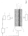
- a SiO 2 -containing substrate 1 either directly, ie immediately, or via a An oxide-containing reducing agent 4 is arranged between layer 3 with its oxidized surface 5 .
- a backing plate 2 (backing) is arranged, which serves as a pressure plate for the pressing process.
- the back plate 2 can be formed, for example, from metal oxide ceramics, eg aluminum oxide ceramics, if aluminum is used as the reducing agent containing oxide. In this way, an undesired connection between the backing plate 2 and the surface of the oxide-containing reducing agent 4 lying against it is avoided.
- the backing plate 2 or pressure plate may be coated with an inert material, such as molybdenum, on the side against which it rests on the reducing agent. This can prevent the back plate from sticking (sticking) too much after the pressing process has been carried out.
- an inert material such as molybdenum
- This arrangement with the layers 1, 2, 4, 5 and optionally also the layer 3 is now subjected to a pressing force on both sides via a pressing die 7 and accordingly to a pressing pressure for the implementation of the method according to the invention.
- the system used for this has a drive unit 9 for actuating the press ram 7 .
- a heating device 8 is present for carrying out the heating of the arrangement shown.
- the system described can be controlled automatically via a control device 10, for example a computer-controlled control device. Accordingly, the control device 10 can control the drive motor 9 and the heating device 8 .
- an initially relatively high pressure is applied to the intermediate arrangement via the ram 7 .
- the arrangement is heated by the heating device 8 to a process temperature.
- the pressure is reduced.
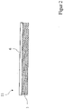
- the process is complete, ie the desired crystalline silicon layer 6 is produced on the surface of the substrate 1 facing the oxide-containing reducing agent 4, such as that figure 2 indicates. In this way, a silicon-based semiconductor component 11 is provided for further applications.
- the oxide-containing reducing agent can also be pressed onto the substrate by means of a roller which is moved over the reducing agent or the backing plate 2 .
- the heating device 8 can be designed as a separate unit or can be integrated into other parts of the system, for example the ram 7, the backing plate 8 and/or a roller if this is used for pressing.
Landscapes
- Chemical & Material Sciences (AREA)
- Organic Chemistry (AREA)
- Inorganic Chemistry (AREA)
- Photovoltaic Devices (AREA)
Description
- Die Erfindung betrifft ein Verfahren zur Herstellung einer kristallinen Siliziumschicht auf der Oberfläche eines SiO2-haltigen Substrats. Die Erfindung betrifft ferner ein siliziumbasiertes Halbleiterbauelement, das nach einem solchen Verfahren hergestellt ist.
- Aus der
DE 10 2014 009 462 A1 und derDE 10 2014 003 941 A1 ist bereits ein Verfahren zur Herstellung von Silizium auf Quarzsubstrat bekannt. Der Erfindung liegt die Aufgabe zugrunde, ein weiter verbessertes Verfahren sowie ein dementsprechend hergestelltes siliziumbasiertes Halbleiterbauelement anzugeben. Diese Aufgabe wird durch ein Verfahren gemäß Anspruch 1 gelöst. Dies umfasst die Herstellung einer kristallinen Siliziumschicht auf der Oberfläche eines SiO2-haltigen Substrats mit den Schritten: - a) Bereitstellen des Substrats ohne die kristalline Siliziumschicht auf der Oberfläche,
- b) Aufbringen eines oxidhaltigen Reduktionsmittels direkt oder über wenigstens eine Zwischenschicht auf der mit der kristallinen Siliziumschicht zu versehenden Oberfläche des Substrats,
- c) Erzeugen der kristallinen Siliziumschicht auf dem Substrat durch Anpressen des oxidhaltigen Reduktionsmittels an das Substrat bei gleichzeitiger Erwärmung der Anordnung auf eine Prozesstemperatur, wobei das oxidhaltige Reduktionsmittel ein oxidhaltiges metallisches Reduktionsmittel ist und die Prozesstemperatur unterhalb der Schmelztemperatur des oxidhaltigen metallischen Reduktionsmittels liegt.
- Die Erfindung hat den Vorteil, dass mit einfachen Mitteln beliebige SiO2-haltige Substrate in Massenproduktion in Bauteile mit einer kristallinen Siliziumschicht konvertiert werden können. Es können beliebige SiO2-haltige Substrate eingesetzt werden, z.B. Inseln, Teilbereiche, Inhaltsstoffe oder nur Oberflächen von einem Trägermaterial. Das Substrat oder Trägermaterial können auch flexible Folien sein. Das SiO2-haltige Substrate oder dessen Oberfläche kann auch strukturiert sein. Es können beispielsweise Substrate in Form von Floatglas-Scheiben oder andere Quarzglassubstrate verwendet werden, dementsprechend kostengünstig konvertiert werden und nach der Konvertierung als siliziumbasiertes Halbleiterbauelement eingesetzt werden. Auf diese Weise können in großem Umfang, sowohl von der Stückzahl her als auch von den baulichen Dimensionen des Bauelementes her, solche Halbleiterbauelemente hergestellt werden, z.B. in Form von Solarzellen, TFT-Displays und anderen siliziumbasierten Halbleiterbauelementen, bis hin zu elektronischen Schaltungen. Vorteilhafterweise sind für diesen Herstellungsprozess keine Reinraumbedingungen erforderlich, insbesondere muss kein Vakuum erzeugt werden. Es muss auch kein Schutzgas verwendet werden. Das SiO2-haltige Substrat kann insbesondere in Form einer flachen bzw. ebenen Platte bereitgestellt werden, z.B. in Form einer Glasplatte. Das SiO2-haltige Substrat kann, abgesehen von vernachlässigbaren Verunreinigungen, aus reinem SiO2 bestehen.
- Ein weiterer Vorteil der Erfindung besteht darin, dass mittels der erläuterten, einfachen Herstellungsschritte eine Siliziumschicht mit hoher Reinheit bereitgestellt werden kann, die auch ohne nachfolgende Weiterverarbeitungsschritte bereits für Anwendungen in der Photovoltaik oder für andere Halbleiterbauteile geeignet ist. Zudem wird gleich die gewünschte kristalline Struktur des Siliziums bereitgestellt, die darüber hinaus eine feste Verbindung mit dem Substrat aufweist.
- Das oxidhaltige Reduktionsmittel kann jedes oxidhaltige metallische Material sein, das geeignet ist, SiO2 in einer Reduktionsreaktion zu kristallinem Silizium zu konvertieren. Das Reduktionsmittel kann z.B. eine oxidierte Oberfläche aufweisen, mit der es direkt oder über die wenigstens eine Zwischenschicht auf der mit der kristallinen Siliziumschicht zu versehenden Oberfläche des Substrats aufgebracht wird. Das oxidhaltige Reduktionsmittel ist ein oxidhaltiges metallisches Reduktionsmittel, z.B. ein oxidiertes metallisches Reduktionsmittel. Das oxidhaltige metallische Reduktionsmittel kann jedes Metall oder jeder metallähnliche Stoff sein, der geeignet ist, SiO2 in einer Reduktionsreaktion zu kristallinem Silizium zu konvertieren. Geeignet sind beispielsweise Aluminium, Magnesium, Kalium, insbesondere in Form von Erdalkali. Das oxidhaltige Reduktionsmittel kann in unterschiedlichen Konsistenzen eingesetzt werden, z.B. in pastöser Form, wie z.B. Siebdruckpaste, oder in Feststoffform, z.B. als Folie. Als besonders geeignet hat sich z.B. Kondensatorfolie gezeigt. Diese weist aufgrund ihrer Oberflächenrauheit eine besonders große Oberfläche auf, so dass an der Oberfläche eine besonders gut ausgeprägte Metalloxidschicht gebildet wird.
- Wird ein oxidhaltiges Reduktionsmittel in pastöser Form, wie z.B. die Siebdruckpaste, eingesetzt, kann durch diese Paste zugleich eine Dotierung, z.B. eine p-Dotierung mittels Aluminium, des Siliziums der hergestellten kristallinen Siliziumschicht erzeugt werden, zudem können elektrische Leiterbahnen auf der Oberfläche der Siliziumschicht erzeugt werden. Ein Vorteil eines solchen pastösen Reduktionsmittels besteht außerdem darin, dass es seine Position beibehält und nicht zerfließt. Mittels des oxidhaltigen Reduktionsmittels in pastöser Form kann eine strukturierte Siliziumschicht erzeugt werden, z.B. indem das pastöse Reduktionsmittel über eine Maske, die die entsprechende Strukturierung beinhaltet, auf dem Substrat aufgetragen wird und dementsprechend durch die Reduktionsreaktion nur an bestimmten Stellen, dort wo sich die Paste befindet, die Umwandlung des SiO2 in kristallines Silizium durchgeführt wird.
- Allgemein gilt, dass eine p-Dotierung des Siliziums z.B. mittels Aluminium und eine n-Dotierung z.B. mittels Magnesium als Reduktionsmittel erzeugt werden.
- Das oxidhaltige Reduktionsmittel kann auch in gasförmiger Phase auf das Substrat aufgebracht werden, z.B. durch einen Aufdampfprozess. Versuche haben gezeigt, dass es beispielsweise vorteilhaft für die Erzeugung einer hochreinen kristallinen Siliziumschicht ist, wenn das oxidhaltige Reduktionsmittel in mehreren einzelnen Schritten aufgedampft wird und zwischen diesen Schritten eine Entlüftung in der Aufdampfkammer der Aufdampfanlage durchgeführt wird. Auf diese Weise wird die gerade aufgedampfte Metalloxidschicht oxidiert. Durch mehrfaches Wiederholen dieses Prozesses können dünne Metalloxidschichten erzeugt werden, die eine gute Basis für die nachfolgende Umwandlung des SiO2 in das kristalline Silizium bildet. Bei dem Aufdampfprozess kann zum Abschluss ein längerer Aufdampfvorgang des oxidhaltigen Reduktionsmittels erfolgen, um eine dickere Abschlussschicht aus diesem Material zu erzeugen.
- Eine strukturierte Ausbildung der kristallinen Siliziumschicht kann auch dadurch hergestellt werden, dass das Aufdampfen des oxidhaltigen Reduktionsmittels über eine Maske durchgeführt wird, die die entsprechende Strukturierung beinhaltet.
- Beim Aufdampfprozess kann z.B. ein Dotiermaterial beigegeben werden, um die entstehende Siliziumschicht mit einer Dotierung zu versehen.
- Das Aufbringen des oxidhaltigen Reduktionsmittels gemäß Schritt b) kann auch durch Aufwalzen erfolgen, z.B. dadurch, dass das oxidhaltige Reduktionsmittel mit der oxidierten Oberfläche unter Druck und ggf. unter Erwärmung auf das Substrat oder die Zwischenschicht aufgewalzt wird. Danach kann das Erzeugen der kristallinen Siliziumschicht gemäß Schritt c) erfolgen. Die Erwärmung bzw. die dadurch erreichte Prozesstemperatur kann vom Schritt b) zum Schritt c) erhöht werden.
- In jedem der zuvor erläuterten Fälle kann eine Strukturierung der kristallinen Siliziumschicht auch dadurch hergestellt werden, dass das Anpressen des oxidhaltigen Reduktionsmittels an das Substrat mittels einer strukturierten Druckplatte erfolgt, d.h. einer Druckplatte, die entsprechend der gewünschten Strukturierung der Siliziumschicht entsprechende Erhebungen und Vertiefungen aufweist. An denjenigen Stellen, an denen das SiO2 in kristallines Silizium umgewandelt werden soll, weist die Druckplatte jeweils eine Erhebung auf, sodass an diesen Stellen Druck auf das oxidhaltige Reduktionsmittel ausgeübt wird. An denjenigen Stellen, an denen die Druckplatte Vertiefungen aufweist, wird kein entsprechender Anpressdruck auf das oxidhaltige Reduktionsmittel ausgeübt, sodass darunter auch keine Umwandlung des SiO2 in kristallines Silizium erfolgt.
- Ferner kann eine Strukturierung der kristallinen Siliziumschicht auch durch lokale Lasererhitzung hergestellt werden.
- Das oxidhaltige Reduktionsmittel mit oder ohne seine oxidierte Oberfläche kann auch zunächst auf einem anderen Bauelement vorbereitet werden als auf dem Substrat, z.B. auf einer Folie. Von diesem anderen Bauelement kann das so mit der oxidierten Oberfläche vorbereitete oxidhaltige Reduktionsmittel dann auf das Substrat übertragen werden, z.B. durch Anpressen, insbesondere bei gleichzeitiger Erwärmung der Anordnung.
- Die auf der mit der kristallinen Siliziumschicht zu versehenden Oberfläche des Substrats aufzubringende Schicht oder die Schichten, z.B. des oxidhaltigen Reduktionsmittels und/oder die Zwischenschicht, können auch mittels galvanischer und/oder elektrochemischer Prozesse aufgebracht werden, z.B. durch Eloxieren.
- Die gesamte Dauer des Verfahrens, bis die kristalline Siliziumschicht in der gewünschten Weise erzeugt ist, kann im Bereich von 30 Minuten bis fünf Stunden liegen.
- Gemäß einer vorteilhaften Weiterbildung der Erfindung ist vorgesehen, dass das Anpressen mit einem anfänglich hohen Pressdruck erfolgt, der im weiteren Verlauf des Anpressvorgangs reduziert wird. Auf diese Weise kann trotz Reduzierung des Pressdrucks das erfindungsgemäße Verfahren relativ schnell durchgeführt werden. Die Reduzierung des Pressdrucks vom anfänglich hohen Wert kann beispielsweise in einer oder mehreren Stufen erfolgen und/oder mit stufenlosen Übergängen, z.B. nach einer Abklingfunktion. So kann z.B. der anfänglich hohe Pressdruck für einen kurzen Zeitraum aufrechterhalten werden, z.B. für einen Zeitraum bis zu einer halben Stunde, und danach ein verringerter Pressdruck für einen Zeitraum von z.B. ein bis drei Stunden.
- Der Pressdruck, insbesondere der anfänglich hohe Pressdruck kann im Bereich von < 1,5 MPa liegen, oder < 1 MPa, somit bei relativ geringen Werten. Solche Pressdruckwerte lassen sich auch mit einfachen Geräten und Anlagen erzeugen. Je nach Art und Weise der Durchführung des Verfahrens ist der erforderliche Mindest-Pressdruck wahlweise festzulegen, z.B. bei einem Mindestwert von 20 kPa oder 50 kPa.
- Gemäß der Erfindung ist vorgesehen, dass die Prozesstemperatur unterhalb der Schmelztemperatur des metallischen Reduktionsmittels liegt. Auf diese Weise kann ein Niedertemperatur-Herstellprozess für die kristalline Siliziumschicht auf der Oberfläche des SiO2-haltigen Substrats bereitgestellt werden. Es sind insbesondere keine Erwärmungsprozesse auf extrem hohe Prozesstemperaturen erforderlich, es reichen beispielsweise Temperaturen im Bereich von 600°C, wenn Aluminium als Reduktionsmittel eingesetzt wird.
- Gemäß einer vorteilhaften Weiterbildung der Erfindung ist vorgesehen, dass die Prozesstemperatur im Bereich von +/- 50°C im Bereich der Glasübergangstemperatur des Substrats liegt. Auch hierdurch kann ein günstiger, relativ niedriger Temperaturbereich für die Prozesstemperatur genutzt werden. Liegt die Glasübergangstemperatur des SiO2-haltigen Substrats beispielsweise im Bereich von 600°C bis 630°C, so kann die Prozesstemperatur beispielsweise geringfügig geringer festgelegt werden, z.B. bei 590°C. Allgemein gilt, dass die Prozesstemperatur dann im Bereich von 550°C bis 680°C festgelegt werden kann.
- Gemäß einer vorteilhaften Weiterbildung der Erfindung ist vorgesehen, dass die kristalline Siliziumschicht als Dünnschicht mit einer Schichtdicke von maximal 100 µm, insbesondere maximal 50 µm, erzeugt wird. Auf diese Weise lassen sich relativ homogene Dünnschichten der kristallinen Siliziumschicht bereitstellen, die ohne aufwendige Nachbearbeitung bereits die Grundlage für die Nutzung als siliziumbasiertes Halbleiterbauelement bilden können.
- Gemäß einer vorteilhaften Weiterbildung der Erfindung ist vorgesehen, dass die kristalline Siliziumschicht mit Korngrößen im Bereich von nanokristallin bis multikristallin erzeugt wird. Auf diese Weise kann ein konstruktives Ausgangsmaterial beispielsweise für die gebäudeintegrierende Photovoltaik, TFT-Displays oder andere Halbleiterbauelemente bereitgestellt werden.
- Gemäß einer vorteilhaften Weiterbildung der Erfindung ist vorgesehen, dass das Verfahren ohne Vakuum und ohne Schutzgas durchgeführt wird. Dementsprechend ist das Verfahren mit einfachen Mitteln, insbesondere mit wenig aufwendigen Geräten und Anlagen, durchführbar.
- Gemäß einer vorteilhaften Weiterbildung der Erfindung ist vorgesehen, dass als Zwischenschicht zwischen dem oxidhaltigen Reduktionsmittels und der mit der kristallinen Siliziumschicht zu versehenden Oberfläche des Substrats eine Schicht aus einem weiteren oxidhaltigen Reduktionsmittel angeordnet wird und dann die Erzeugung der kristallinen Siliziumschicht durchgeführt wird. Durch die Zwischenschicht kann der Konvertierungsprozess des SiO2 des Substrats in die kristalline Siliziumschicht weiter optimiert werden. Die Zwischenschicht kann auch ein bereits oxidiertes Material aufweisen oder daraus bestehen.
- Insbesondere kann als Zwischenschicht zwischen der Oxidschicht des metallischen Reduktionsmittels und der mit der kristallinen Siliziumschicht zu versehenden Oberfläche des Substrats eine Schicht aus einem weiteren metallischen Reduktionsmittel angeordnet und dann die Erzeugung der kristallinen Siliziumschicht durchgeführt werden.
- Gemäß einer vorteilhaften Weiterbildung der Erfindung ist vorgesehen, dass das weitere oxidhaltige Reduktionsmittel gleich dem erstgenannten oxidhaltigen Reduktionsmittel ist. Auf diese Weise können unerwünschte Verunreinigungen durch Fremdmaterialien vermieden werden.
- Beschrieben wird ferner ein siliziumbasiertes Halbleiterbauelement, das nach einem Verfahren der zuvor erläuterten Art hergestellt ist. Das Halbleiterbauelement kann z.B. eine Solarzelle, ein TFT-Display oder ein sonstiges Halbleiterbauelement sein, einschließlich einer elektronischen Schaltung mit mehreren einzelnen Halbleiterbauelementen, die durch Strukturierung und/oder Dotierung der kristallinen Siliziumschicht hergestellt sind. Die Erfindung eignet sich somit für Halbleiterbauelemente nicht nur in kleiner Bauform, sondern auch für großflächige Halbleitersysteme, wobei die Substrate auch flexible Folien sein können, z.B. TFT-Displays oder Photovoltaik-Anwendungen jeglicher Bauform.
- Das oxidhaltige Reduktionsmittel kann insbesondere in Feststoffform bereitgestellt werden, z. B. als Metallfolie oder dünnes Metallblech.
- Das erfindungsgemäße Verfahren kann insbesondere ohne besondere Vorbehandlung des oxidhaltigen Reduktionsmittels erfolgen, es ist insbesondere nicht erforderlich, eine eventuell bereits oxidierte Oberfläche des oxidhaltigen Reduktionsmittels zunächst zu entfernen. Vielmehr kann eine solche vorhandene Oxidschicht vorteilhaft zur Durchführung des Verfahrens genutzt werden, was überraschend ist und nicht zu erwarten ist, da oxidierte Oberflächen beispielsweise von Aluminium oder Magnesium als ungeeignet für die Durchführung einer chemischen Reaktion gelten. Das erfindungsgemäße Verfahren kann ganz oder zumindest hauptsächlich als Festkörper-Reaktion durchgeführt werden, insbesondere ohne einen Verflüssigungsvorgang bzw. Schmelzvorgangs des oxidhaltigen Reduktionsmittels. Die Erwärmung der Anordnung auf die Prozesstemperatur kann daher auf eine Temperatur unterhalb der Schmelztemperatur des oxidhaltigen Reduktionsmittels erfolgen. Bei der Durchführung der chemischen Reaktion, bei der die kristalline Siliziumschicht auf dem Substrat durch Anpressen des oxidhaltigen Reduktionsmittels an das Substrat erfolgt, können lokal begrenzte Übergangsstellen auftreten, an denen ein Übergang in eine flüssige Phase zwischen den beteiligten Elementen erfolgen kann.
- Insbesondere kann die Prozesstemperatur deutlich unterhalb der Schmelztemperatur einer oxidierten Oberfläche des oxidhaltigen Reduktionsmittels liegen, z. B. unterhalb des Schmelzpunkts einer Aluminiumoxidschicht, der bei ca. 2050 °C liegt. Im Falle der Verwendung von Aluminium als oxidhaltiges Reduktionsmittel kann die Prozesstemperatur bei maximal 630 °C liegen. Es ist damit eine Herstellung von kristallinem Silizium bei vergleichsweise geringen Temperaturen möglich.
- Die Erfindung wird nachfolgend anhand eines Ausführungsbeispiels unter Verwendung von Zeichnungen näher erläutert. Die Zeichnungen zeigen in
- Figur 1
- eine Anordnung zur Herstellung der kristallinen Siliziumschicht in seitlicher Schnittdarstellung und
- Figur 2
- ein siliziumbasiertes Halbleiterbauelement in seitlicher Schnittdarstellung.
- Wie erkennbar ist, ist auf einer in der
Figur 1 nach oben gerichteten Oberfläche eines SiO2-haltigen Substrats 1 entweder direkt, d.h. unmittelbar, oder über eine Zwischenschicht 3 ein oxidhaltiges Reduktionsmittel 4 mit seiner oxidierten Oberfläche 5 angeordnet. Auf der Rückseite, d.h. der von der Metalloxidschicht 5 abgewandten Seite des oxidhaltigen Reduktionsmittels 4, ist eine Rückenplatte 2 (Backing) angeordnet, die als Druckplatte für den Anpressvorgang dient. Die Rückenplatte 2 kann beispielsweise aus Metalloxidkeramik ausgebildet sein, z.B. Aluminiumoxidkeramik, wenn als oxidhaltiges Reduktionsmittel Aluminium eingesetzt wird. Auf diese Weise wird eine unerwünschte Verbindung zwischen der Rückenplatte 2 und der daran anliegenden Oberfläche des oxidhaltigen Reduktionsmittels 4 vermieden. - Die Rückenplatte 2 oder Druckplatte kann an der Seite, an der sie auf dem Reduktionsmittel anliegt, mit einem inerten Material beschichtet sein, z.B. mit Molybdän. Hierdurch kann vermieden werden, dass die Rückenplatte nach Durchführung des Anpressvorgangs zu sehr festhaftet (festklebt).
- Diese Anordnung mit den Schichten 1, 2, 4, 5 und gegebenenfalls noch der Schicht 3 wird für die Durchführung des erfindungsgemäßen Verfahrens nun über Pressstempel 7 beidseitig mit einer Presskraft und dementsprechend mit einem Pressdruck beaufschlagt. Die hierfür eingesetzte Anlage weist eine Antriebseinheit 9 zur Betätigung der Pressstempel 7 auf. Ferner ist zur Durchführung der Erwärmung der dargestellten Anordnung eine Erwärmungseinrichtung 8 vorhanden. Die beschriebene Anlage kann über eine Steuereinrichtung 10, z.B. eine computergesteuerte Steuereinrichtung, automatisch gesteuert werden. Dementsprechend kann die Steuereinrichtung 10 den Antriebsmotor 9 und die Erwärmungseinrichtung 8 steuern. Für die Durchführung des erfindungsgemäßen Verfahrens wird über die Pressstempel 7 ein zunächst relativ hoher Pressdruck auf die dazwischenliegende Anordnung aufgebracht. Gleichzeitig erfolgt eine Erwärmung der Anordnung durch die Erwärmungseinrichtung 8 auf eine Prozesstemperatur. Nach einer bestimmten Einwirkzeit wird der Pressdruck verringert. Schließlich ist das Verfahren vollständig durchgeführt, d.h. es ist auf der zum oxidhaltigen Reduktionsmittel 4 gerichteten Oberfläche des Substrats 1 die gewünschte kristalline Siliziumschicht 6 erzeugt, wie die
Figur 2 zeigt. Auf diese Weise wird ein siliziumbasiertes Halbleiterbauelement 11 für weitere Anwendungen bereitgestellt. - Das Anpressen des oxidhaltigen Reduktionsmittels an das Substrat kann auch mittels einer Walze erfolgen, die über das Reduktionsmittel oder die Rückenplatte 2 bewegt wird.
- Die Erwärmungseinrichtung 8 kann als separate Einheit ausgebildet sein oder in andere Teile der Anlage integriert sein, z.B. in den Pressstempel 7, die Rückenplatte 8 und/oder eine Walze, wenn diese zum Anpressen genutzt wird.
Claims (8)
- Verfahren zur Herstellung einer kristallinen Siliziumschicht (6) auf der Oberfläche eines SiO2-haltigen Substrats (1) mit den Schritten:a) Bereitstellen des Substrats (1) ohne die kristalline Siliziumschicht (6) auf der Oberfläche,b) Aufbringen eines oxidhaltigen Reduktionsmittels (4) direkt oder über wenigstens eine Zwischenschicht (3) auf der mit der kristallinen Siliziumschicht (6) zu versehenden Oberfläche des Substrats (1),c) Erzeugen der kristallinen Siliziumschicht (6) auf dem Substrat (1) durch Anpressen des oxidhaltigen Reduktionsmittels (4) an das Substrat (1) bei gleichzeitiger Erwärmung der Anordnung auf eine Prozesstemperatur,dadurch gekennzeichnet, dass das oxidhaltige Reduktionsmittel (4) ein oxidhaltiges metallisches Reduktionsmittel (4) ist und die Prozesstemperatur unterhalb der Schmelztemperatur des oxidhaltigen metallischen Reduktionsmittels (4) liegt.
- Verfahren nach dem vorhergehenden Anspruch, dadurch gekennzeichnet, dass das Anpressen mit einem anfänglich hohen Pressdruck erfolgt, der im weiteren Verlauf des Anpressvorgangs reduziert wird.
- Verfahren nach einem der vorhergehenden Ansprüche, dadurch gekennzeichnet, dass das Anpressen mit einem Pressdruck von weniger als 1,5 MPa erfolgt.
- Verfahren nach einem der vorhergehenden Ansprüche, dadurch gekennzeichnet, dass die Prozesstemperatur im Bereich von +/- 50°C im Bereich der Glasübergangstemperatur des Substrats (1) liegt.
- Verfahren nach einem der vorhergehenden Ansprüche, dadurch gekennzeichnet, dass die kristalline Siliziumschicht (6) als Dünnschicht mit einer Schichtdicke von maximal 100 µm erzeugt wird.
- Verfahren nach einem der vorhergehenden Ansprüche, dadurch gekennzeichnet, dass das Verfahren ohne Vakuum und ohne Schutzgas durchgeführt wird.
- Verfahren nach einem der vorhergehenden Ansprüche, dadurch gekennzeichnet, dass als Zwischenschicht (3) zwischen dem oxidhaltigen metallischen Reduktionsmittel (4) und der mit der kristallinen Siliziumschicht (6) zu versehenden Oberfläche des Substrats (1) eine Schicht aus einem weiteren oxidhaltigen Reduktionsmittel angeordnet wird und dann die Erzeugung der kristallinen Siliziumschicht (6) durchgeführt wird.
- Verfahren nach Anspruch 7, dadurch gekennzeichnet, dass das weitere oxidhaltige Reduktionsmittel gleich dem erstgenannten oxidhaltigen metallischen Reduktionsmittel (4) ist.
Applications Claiming Priority (2)
| Application Number | Priority Date | Filing Date | Title |
|---|---|---|---|
| DE102016117182.4A DE102016117182A1 (de) | 2016-09-13 | 2016-09-13 | Verfahren zur Herstellung einer kristallinen Siliziumschicht und siliziumbasiertes Halbleiterbauelement |
| PCT/EP2017/072642 WO2018050565A1 (de) | 2016-09-13 | 2017-09-08 | Verfahren zur herstellung einer kristallinen siliziumschicht und siliziumbasiertes halbleiterbauelement |
Publications (2)
| Publication Number | Publication Date |
|---|---|
| EP3513425A1 EP3513425A1 (de) | 2019-07-24 |
| EP3513425B1 true EP3513425B1 (de) | 2022-11-16 |
Family
ID=59930325
Family Applications (1)
| Application Number | Title | Priority Date | Filing Date |
|---|---|---|---|
| EP17771694.1A Active EP3513425B1 (de) | 2016-09-13 | 2017-09-08 | Verfahren zur herstellung einer kristallinen siliziumschicht und siliziumbasiertes halbleiterbauelement |
Country Status (3)
| Country | Link |
|---|---|
| EP (1) | EP3513425B1 (de) |
| DE (1) | DE102016117182A1 (de) |
| WO (1) | WO2018050565A1 (de) |
Families Citing this family (2)
| Publication number | Priority date | Publication date | Assignee | Title |
|---|---|---|---|---|
| DE102022001466A1 (de) | 2022-04-26 | 2023-10-26 | Jpm Silicon Gmbh | Verfahren und Vorrichtung zur Gewinnung von Siliziummonoxid und Silizium |
| DE102022001511A1 (de) | 2022-04-29 | 2023-11-02 | Jpm Silicon Gmbh | Verfahren und Vorrichtung zur Herstellung von Silizium-Schichten auf SiO2-Substraten |
Family Cites Families (3)
| Publication number | Priority date | Publication date | Assignee | Title |
|---|---|---|---|---|
| US20120230904A1 (en) | 2009-08-25 | 2012-09-13 | Mansoor Barati | Production of high purity silicon from amorphous silica |
| DE102014003941A1 (de) * | 2014-03-20 | 2015-09-24 | Sameday Media Gmbh | Verfahren zur Herstellung kristallinen Reinstsiliciums auf Quarzsubstrat |
| DE102014009462A1 (de) | 2014-06-30 | 2015-12-31 | Sameday Media Gmbh | Verfahren zur Herstellung von Silicium auf Quarzsubstrat |
-
2016
- 2016-09-13 DE DE102016117182.4A patent/DE102016117182A1/de not_active Ceased
-
2017
- 2017-09-08 WO PCT/EP2017/072642 patent/WO2018050565A1/de not_active Ceased
- 2017-09-08 EP EP17771694.1A patent/EP3513425B1/de active Active
Also Published As
| Publication number | Publication date |
|---|---|
| WO2018050565A1 (de) | 2018-03-22 |
| DE102016117182A1 (de) | 2018-03-15 |
| EP3513425A1 (de) | 2019-07-24 |
Similar Documents
| Publication | Publication Date | Title |
|---|---|---|
| DE69825517T2 (de) | Herstellungsverfahren eines Halbleiter-Substrats | |
| DE4415132C2 (de) | Verfahren zur formgebenden Bearbeitung von dünnen Wafern und Solarzellen aus kristallinem Silizium | |
| EP2299496B1 (de) | Verfahren zur Herstellung eines Kontaktbereichs eines elektronischen Bauteils | |
| EP1261990A1 (de) | Flexibles metallisches substrat für cis-solarzellen und verfahren zu seiner herstellung | |
| DE112008003144T5 (de) | Schichtstruktur von CIS Solarzelle, integrierte Struktur von CIS Dünnschichtsolarzelle sowie deren Herstellungsverfahren | |
| DE102010021764A1 (de) | Verfahren zur Niedertemperatur Drucksinterverbindung zweier Verbindungspartner und hiermit hergestellte Anordnung | |
| DE102009010816A1 (de) | Verfahren zur Herstellung eines Halbleiter-Bauelements | |
| DE102018202513A1 (de) | Verfahren zur Metallisierung eines Bauelements | |
| DE102011016335A1 (de) | Nickelhaltige und ätzende druckbare Paste insbesondere zur Kontaktbildung mit Silizium beim Herstellen einer Solarzelle | |
| DE3790981B4 (de) | Verfahren zum Herstellen einer Photovoltaik-Solarzelle | |
| EP3513425B1 (de) | Verfahren zur herstellung einer kristallinen siliziumschicht und siliziumbasiertes halbleiterbauelement | |
| EP2561557A2 (de) | Verfahren zur herstellung einer solarzelle sowie nach diesem verfahren hergestellte solarzelle | |
| DE102012216026B4 (de) | Verfahren zur Herstellung einer flexiblen Photovoltaik-Dünnschichtzelle mit einer Eisendiffusionsbarriereschicht und flexible Photovoltaik-Dünnschichtzelle mit einer Eisendiffusionsbarriereschicht | |
| DE10259258B4 (de) | Verfahren zur Herstellung einer Verbindungshalbleiterschicht mit Alkalimetallzusatz | |
| DE19917758C2 (de) | Verfahren zur Herstellung einer CuInSe2(CIS)Solarzelle | |
| DE102017117668B3 (de) | Leistungselektronische Anordnung mit einer Haftschicht sowie Verfahren zur Herstellung dieser Anordnung | |
| WO2003097557A1 (de) | Verfahren zum herstellen eines keramik-kupfer-verbundsubstrats | |
| EP1241148B1 (de) | AIuminiumnitridsubstrat sowie Verfahren zur Vorbereitung dieses Substrates auf die Verbindung mit einer Kupferfolie | |
| DE10006823A1 (de) | Flexibles metallisches Substrat für CIS-Solarzellen und Verfahren zu seiner Herstellug | |
| CH670335A5 (de) | ||
| DE10004733C2 (de) | Dünnfilm-Halbleiterbauelement mit einer Chalkopyritschicht und Verfahren zu seiner Herstellung sowie Verwendung des Verfahrens zur Herstellung einer Dünnfilm-Solarzelle | |
| DE19802131A1 (de) | Verfahren zur Herstellung einer monokristallinen Schicht aus einem leitenden oder halbleitenden Material | |
| DE10127255A1 (de) | Konditionierung von Glasoberflächen für den Transfer von CIGS-Solarzellen auf flexible Kunstoffsubstrate | |
| EP3049546B1 (de) | Verfahren zur herstellung der rückkontaktschicht für cdte-dünnschicht-solarzellen | |
| CH669476A5 (de) |
Legal Events
| Date | Code | Title | Description |
|---|---|---|---|
| STAA | Information on the status of an ep patent application or granted ep patent |
Free format text: STATUS: UNKNOWN |
|
| STAA | Information on the status of an ep patent application or granted ep patent |
Free format text: STATUS: THE INTERNATIONAL PUBLICATION HAS BEEN MADE |
|
| PUAI | Public reference made under article 153(3) epc to a published international application that has entered the european phase |
Free format text: ORIGINAL CODE: 0009012 |
|
| STAA | Information on the status of an ep patent application or granted ep patent |
Free format text: STATUS: REQUEST FOR EXAMINATION WAS MADE |
|
| 17P | Request for examination filed |
Effective date: 20190312 |
|
| AK | Designated contracting states |
Kind code of ref document: A1 Designated state(s): AL AT BE BG CH CY CZ DE DK EE ES FI FR GB GR HR HU IE IS IT LI LT LU LV MC MK MT NL NO PL PT RO RS SE SI SK SM TR |
|
| AX | Request for extension of the european patent |
Extension state: BA ME |
|
| DAV | Request for validation of the european patent (deleted) | ||
| DAX | Request for extension of the european patent (deleted) | ||
| STAA | Information on the status of an ep patent application or granted ep patent |
Free format text: STATUS: EXAMINATION IS IN PROGRESS |
|
| 17Q | First examination report despatched |
Effective date: 20200814 |
|
| GRAP | Despatch of communication of intention to grant a patent |
Free format text: ORIGINAL CODE: EPIDOSNIGR1 |
|
| STAA | Information on the status of an ep patent application or granted ep patent |
Free format text: STATUS: GRANT OF PATENT IS INTENDED |
|
| INTG | Intention to grant announced |
Effective date: 20220608 |
|
| GRAS | Grant fee paid |
Free format text: ORIGINAL CODE: EPIDOSNIGR3 |
|
| GRAA | (expected) grant |
Free format text: ORIGINAL CODE: 0009210 |
|
| STAA | Information on the status of an ep patent application or granted ep patent |
Free format text: STATUS: THE PATENT HAS BEEN GRANTED |
|
| AK | Designated contracting states |
Kind code of ref document: B1 Designated state(s): AL AT BE BG CH CY CZ DE DK EE ES FI FR GB GR HR HU IE IS IT LI LT LU LV MC MK MT NL NO PL PT RO RS SE SI SK SM TR |
|
| REG | Reference to a national code |
Ref country code: GB Ref legal event code: FG4D Free format text: NOT ENGLISH |
|
| REG | Reference to a national code |
Ref country code: CH Ref legal event code: EP |
|
| REG | Reference to a national code |
Ref country code: IE Ref legal event code: FG4D Free format text: LANGUAGE OF EP DOCUMENT: GERMAN |
|
| REG | Reference to a national code |
Ref country code: DE Ref legal event code: R096 Ref document number: 502017014100 Country of ref document: DE |
|
| REG | Reference to a national code |
Ref country code: AT Ref legal event code: REF Ref document number: 1532286 Country of ref document: AT Kind code of ref document: T Effective date: 20221215 |
|
| REG | Reference to a national code |
Ref country code: LT Ref legal event code: MG9D |
|
| REG | Reference to a national code |
Ref country code: NL Ref legal event code: MP Effective date: 20221116 |
|
| PG25 | Lapsed in a contracting state [announced via postgrant information from national office to epo] |
Ref country code: SE Free format text: LAPSE BECAUSE OF FAILURE TO SUBMIT A TRANSLATION OF THE DESCRIPTION OR TO PAY THE FEE WITHIN THE PRESCRIBED TIME-LIMIT Effective date: 20221116 Ref country code: PT Free format text: LAPSE BECAUSE OF FAILURE TO SUBMIT A TRANSLATION OF THE DESCRIPTION OR TO PAY THE FEE WITHIN THE PRESCRIBED TIME-LIMIT Effective date: 20230316 Ref country code: NO Free format text: LAPSE BECAUSE OF FAILURE TO SUBMIT A TRANSLATION OF THE DESCRIPTION OR TO PAY THE FEE WITHIN THE PRESCRIBED TIME-LIMIT Effective date: 20230216 Ref country code: LT Free format text: LAPSE BECAUSE OF FAILURE TO SUBMIT A TRANSLATION OF THE DESCRIPTION OR TO PAY THE FEE WITHIN THE PRESCRIBED TIME-LIMIT Effective date: 20221116 Ref country code: FI Free format text: LAPSE BECAUSE OF FAILURE TO SUBMIT A TRANSLATION OF THE DESCRIPTION OR TO PAY THE FEE WITHIN THE PRESCRIBED TIME-LIMIT Effective date: 20221116 Ref country code: ES Free format text: LAPSE BECAUSE OF FAILURE TO SUBMIT A TRANSLATION OF THE DESCRIPTION OR TO PAY THE FEE WITHIN THE PRESCRIBED TIME-LIMIT Effective date: 20221116 |
|
| PG25 | Lapsed in a contracting state [announced via postgrant information from national office to epo] |
Ref country code: RS Free format text: LAPSE BECAUSE OF FAILURE TO SUBMIT A TRANSLATION OF THE DESCRIPTION OR TO PAY THE FEE WITHIN THE PRESCRIBED TIME-LIMIT Effective date: 20221116 Ref country code: PL Free format text: LAPSE BECAUSE OF FAILURE TO SUBMIT A TRANSLATION OF THE DESCRIPTION OR TO PAY THE FEE WITHIN THE PRESCRIBED TIME-LIMIT Effective date: 20221116 Ref country code: LV Free format text: LAPSE BECAUSE OF FAILURE TO SUBMIT A TRANSLATION OF THE DESCRIPTION OR TO PAY THE FEE WITHIN THE PRESCRIBED TIME-LIMIT Effective date: 20221116 Ref country code: IS Free format text: LAPSE BECAUSE OF FAILURE TO SUBMIT A TRANSLATION OF THE DESCRIPTION OR TO PAY THE FEE WITHIN THE PRESCRIBED TIME-LIMIT Effective date: 20230316 Ref country code: HR Free format text: LAPSE BECAUSE OF FAILURE TO SUBMIT A TRANSLATION OF THE DESCRIPTION OR TO PAY THE FEE WITHIN THE PRESCRIBED TIME-LIMIT Effective date: 20221116 Ref country code: GR Free format text: LAPSE BECAUSE OF FAILURE TO SUBMIT A TRANSLATION OF THE DESCRIPTION OR TO PAY THE FEE WITHIN THE PRESCRIBED TIME-LIMIT Effective date: 20230217 |
|
| PG25 | Lapsed in a contracting state [announced via postgrant information from national office to epo] |
Ref country code: NL Free format text: LAPSE BECAUSE OF FAILURE TO SUBMIT A TRANSLATION OF THE DESCRIPTION OR TO PAY THE FEE WITHIN THE PRESCRIBED TIME-LIMIT Effective date: 20221116 |
|
| PG25 | Lapsed in a contracting state [announced via postgrant information from national office to epo] |
Ref country code: SM Free format text: LAPSE BECAUSE OF FAILURE TO SUBMIT A TRANSLATION OF THE DESCRIPTION OR TO PAY THE FEE WITHIN THE PRESCRIBED TIME-LIMIT Effective date: 20221116 Ref country code: RO Free format text: LAPSE BECAUSE OF FAILURE TO SUBMIT A TRANSLATION OF THE DESCRIPTION OR TO PAY THE FEE WITHIN THE PRESCRIBED TIME-LIMIT Effective date: 20221116 Ref country code: EE Free format text: LAPSE BECAUSE OF FAILURE TO SUBMIT A TRANSLATION OF THE DESCRIPTION OR TO PAY THE FEE WITHIN THE PRESCRIBED TIME-LIMIT Effective date: 20221116 Ref country code: DK Free format text: LAPSE BECAUSE OF FAILURE TO SUBMIT A TRANSLATION OF THE DESCRIPTION OR TO PAY THE FEE WITHIN THE PRESCRIBED TIME-LIMIT Effective date: 20221116 Ref country code: CZ Free format text: LAPSE BECAUSE OF FAILURE TO SUBMIT A TRANSLATION OF THE DESCRIPTION OR TO PAY THE FEE WITHIN THE PRESCRIBED TIME-LIMIT Effective date: 20221116 |
|
| REG | Reference to a national code |
Ref country code: DE Ref legal event code: R097 Ref document number: 502017014100 Country of ref document: DE |
|
| PG25 | Lapsed in a contracting state [announced via postgrant information from national office to epo] |
Ref country code: SK Free format text: LAPSE BECAUSE OF FAILURE TO SUBMIT A TRANSLATION OF THE DESCRIPTION OR TO PAY THE FEE WITHIN THE PRESCRIBED TIME-LIMIT Effective date: 20221116 Ref country code: AL Free format text: LAPSE BECAUSE OF FAILURE TO SUBMIT A TRANSLATION OF THE DESCRIPTION OR TO PAY THE FEE WITHIN THE PRESCRIBED TIME-LIMIT Effective date: 20221116 |
|
| PLBE | No opposition filed within time limit |
Free format text: ORIGINAL CODE: 0009261 |
|
| STAA | Information on the status of an ep patent application or granted ep patent |
Free format text: STATUS: NO OPPOSITION FILED WITHIN TIME LIMIT |
|
| 26N | No opposition filed |
Effective date: 20230817 |
|
| PG25 | Lapsed in a contracting state [announced via postgrant information from national office to epo] |
Ref country code: SI Free format text: LAPSE BECAUSE OF FAILURE TO SUBMIT A TRANSLATION OF THE DESCRIPTION OR TO PAY THE FEE WITHIN THE PRESCRIBED TIME-LIMIT Effective date: 20221116 |
|
| PG25 | Lapsed in a contracting state [announced via postgrant information from national office to epo] |
Ref country code: LU Free format text: LAPSE BECAUSE OF NON-PAYMENT OF DUE FEES Effective date: 20230908 |
|
| REG | Reference to a national code |
Ref country code: BE Ref legal event code: MM Effective date: 20230930 |
|
| GBPC | Gb: european patent ceased through non-payment of renewal fee |
Effective date: 20230908 |
|
| PG25 | Lapsed in a contracting state [announced via postgrant information from national office to epo] |
Ref country code: LU Free format text: LAPSE BECAUSE OF NON-PAYMENT OF DUE FEES Effective date: 20230908 Ref country code: IT Free format text: LAPSE BECAUSE OF FAILURE TO SUBMIT A TRANSLATION OF THE DESCRIPTION OR TO PAY THE FEE WITHIN THE PRESCRIBED TIME-LIMIT Effective date: 20221116 Ref country code: MC Free format text: LAPSE BECAUSE OF FAILURE TO SUBMIT A TRANSLATION OF THE DESCRIPTION OR TO PAY THE FEE WITHIN THE PRESCRIBED TIME-LIMIT Effective date: 20221116 |
|
| REG | Reference to a national code |
Ref country code: IE Ref legal event code: MM4A |
|
| PG25 | Lapsed in a contracting state [announced via postgrant information from national office to epo] |
Ref country code: IE Free format text: LAPSE BECAUSE OF NON-PAYMENT OF DUE FEES Effective date: 20230908 |
|
| PG25 | Lapsed in a contracting state [announced via postgrant information from national office to epo] |
Ref country code: GB Free format text: LAPSE BECAUSE OF NON-PAYMENT OF DUE FEES Effective date: 20230908 |
|
| PG25 | Lapsed in a contracting state [announced via postgrant information from national office to epo] |
Ref country code: IE Free format text: LAPSE BECAUSE OF NON-PAYMENT OF DUE FEES Effective date: 20230908 Ref country code: GB Free format text: LAPSE BECAUSE OF NON-PAYMENT OF DUE FEES Effective date: 20230908 Ref country code: FR Free format text: LAPSE BECAUSE OF NON-PAYMENT OF DUE FEES Effective date: 20230930 |
|
| PG25 | Lapsed in a contracting state [announced via postgrant information from national office to epo] |
Ref country code: BE Free format text: LAPSE BECAUSE OF NON-PAYMENT OF DUE FEES Effective date: 20230930 |
|
| PG25 | Lapsed in a contracting state [announced via postgrant information from national office to epo] |
Ref country code: BG Free format text: LAPSE BECAUSE OF FAILURE TO SUBMIT A TRANSLATION OF THE DESCRIPTION OR TO PAY THE FEE WITHIN THE PRESCRIBED TIME-LIMIT Effective date: 20221116 |
|
| REG | Reference to a national code |
Ref country code: AT Ref legal event code: MM01 Ref document number: 1532286 Country of ref document: AT Kind code of ref document: T Effective date: 20230908 |
|
| PG25 | Lapsed in a contracting state [announced via postgrant information from national office to epo] |
Ref country code: BG Free format text: LAPSE BECAUSE OF FAILURE TO SUBMIT A TRANSLATION OF THE DESCRIPTION OR TO PAY THE FEE WITHIN THE PRESCRIBED TIME-LIMIT Effective date: 20221116 |
|
| PG25 | Lapsed in a contracting state [announced via postgrant information from national office to epo] |
Ref country code: AT Free format text: LAPSE BECAUSE OF NON-PAYMENT OF DUE FEES Effective date: 20230908 |
|
| PG25 | Lapsed in a contracting state [announced via postgrant information from national office to epo] |
Ref country code: AT Free format text: LAPSE BECAUSE OF NON-PAYMENT OF DUE FEES Effective date: 20230908 |
|
| PG25 | Lapsed in a contracting state [announced via postgrant information from national office to epo] |
Ref country code: CY Free format text: LAPSE BECAUSE OF FAILURE TO SUBMIT A TRANSLATION OF THE DESCRIPTION OR TO PAY THE FEE WITHIN THE PRESCRIBED TIME-LIMIT; INVALID AB INITIO Effective date: 20170908 |
|
| PG25 | Lapsed in a contracting state [announced via postgrant information from national office to epo] |
Ref country code: HU Free format text: LAPSE BECAUSE OF FAILURE TO SUBMIT A TRANSLATION OF THE DESCRIPTION OR TO PAY THE FEE WITHIN THE PRESCRIBED TIME-LIMIT; INVALID AB INITIO Effective date: 20170908 |
|
| REG | Reference to a national code |
Ref country code: CH Ref legal event code: U11 Free format text: ST27 STATUS EVENT CODE: U-0-0-U10-U11 (AS PROVIDED BY THE NATIONAL OFFICE) Effective date: 20251001 |
|
| PGFP | Annual fee paid to national office [announced via postgrant information from national office to epo] |
Ref country code: DE Payment date: 20250919 Year of fee payment: 9 |
|
| REG | Reference to a national code |
Ref country code: DE Ref legal event code: R079 Ref document number: 502017014100 Country of ref document: DE Free format text: PREVIOUS MAIN CLASS: H01L0021180000 Ipc: H10P0014000000 |
|
| PG25 | Lapsed in a contracting state [announced via postgrant information from national office to epo] |
Ref country code: TR Free format text: LAPSE BECAUSE OF FAILURE TO SUBMIT A TRANSLATION OF THE DESCRIPTION OR TO PAY THE FEE WITHIN THE PRESCRIBED TIME-LIMIT Effective date: 20221116 |
|
| PGFP | Annual fee paid to national office [announced via postgrant information from national office to epo] |
Ref country code: CH Payment date: 20251001 Year of fee payment: 9 |