EP3514264A1 - Herstellungsverfahren eines einkristallsiliciums - Google Patents
Herstellungsverfahren eines einkristallsiliciums Download PDFInfo
- Publication number
- EP3514264A1 EP3514264A1 EP19150932.2A EP19150932A EP3514264A1 EP 3514264 A1 EP3514264 A1 EP 3514264A1 EP 19150932 A EP19150932 A EP 19150932A EP 3514264 A1 EP3514264 A1 EP 3514264A1
- Authority
- EP
- European Patent Office
- Prior art keywords
- raw material
- silicon
- silicon raw
- output
- crucible
- Prior art date
- Legal status (The legal status is an assumption and is not a legal conclusion. Google has not performed a legal analysis and makes no representation as to the accuracy of the status listed.)
- Granted
Links
Images


Classifications
-
- C—CHEMISTRY; METALLURGY
- C30—CRYSTAL GROWTH
- C30B—SINGLE-CRYSTAL GROWTH; UNIDIRECTIONAL SOLIDIFICATION OF EUTECTIC MATERIAL OR UNIDIRECTIONAL DEMIXING OF EUTECTOID MATERIAL; REFINING BY ZONE-MELTING OF MATERIAL; PRODUCTION OF A HOMOGENEOUS POLYCRYSTALLINE MATERIAL WITH DEFINED STRUCTURE; SINGLE CRYSTALS OR HOMOGENEOUS POLYCRYSTALLINE MATERIAL WITH DEFINED STRUCTURE; AFTER-TREATMENT OF SINGLE CRYSTALS OR A HOMOGENEOUS POLYCRYSTALLINE MATERIAL WITH DEFINED STRUCTURE; APPARATUS THEREFOR
- C30B15/00—Single-crystal growth by pulling from a melt, e.g. Czochralski method
- C30B15/10—Crucibles or containers for supporting the melt
-
- C—CHEMISTRY; METALLURGY
- C30—CRYSTAL GROWTH
- C30B—SINGLE-CRYSTAL GROWTH; UNIDIRECTIONAL SOLIDIFICATION OF EUTECTIC MATERIAL OR UNIDIRECTIONAL DEMIXING OF EUTECTOID MATERIAL; REFINING BY ZONE-MELTING OF MATERIAL; PRODUCTION OF A HOMOGENEOUS POLYCRYSTALLINE MATERIAL WITH DEFINED STRUCTURE; SINGLE CRYSTALS OR HOMOGENEOUS POLYCRYSTALLINE MATERIAL WITH DEFINED STRUCTURE; AFTER-TREATMENT OF SINGLE CRYSTALS OR A HOMOGENEOUS POLYCRYSTALLINE MATERIAL WITH DEFINED STRUCTURE; APPARATUS THEREFOR
- C30B15/00—Single-crystal growth by pulling from a melt, e.g. Czochralski method
- C30B15/14—Heating of the melt or the crystallised materials
-
- C—CHEMISTRY; METALLURGY
- C30—CRYSTAL GROWTH
- C30B—SINGLE-CRYSTAL GROWTH; UNIDIRECTIONAL SOLIDIFICATION OF EUTECTIC MATERIAL OR UNIDIRECTIONAL DEMIXING OF EUTECTOID MATERIAL; REFINING BY ZONE-MELTING OF MATERIAL; PRODUCTION OF A HOMOGENEOUS POLYCRYSTALLINE MATERIAL WITH DEFINED STRUCTURE; SINGLE CRYSTALS OR HOMOGENEOUS POLYCRYSTALLINE MATERIAL WITH DEFINED STRUCTURE; AFTER-TREATMENT OF SINGLE CRYSTALS OR A HOMOGENEOUS POLYCRYSTALLINE MATERIAL WITH DEFINED STRUCTURE; APPARATUS THEREFOR
- C30B15/00—Single-crystal growth by pulling from a melt, e.g. Czochralski method
- C30B15/20—Controlling or regulating
-
- C—CHEMISTRY; METALLURGY
- C30—CRYSTAL GROWTH
- C30B—SINGLE-CRYSTAL GROWTH; UNIDIRECTIONAL SOLIDIFICATION OF EUTECTIC MATERIAL OR UNIDIRECTIONAL DEMIXING OF EUTECTOID MATERIAL; REFINING BY ZONE-MELTING OF MATERIAL; PRODUCTION OF A HOMOGENEOUS POLYCRYSTALLINE MATERIAL WITH DEFINED STRUCTURE; SINGLE CRYSTALS OR HOMOGENEOUS POLYCRYSTALLINE MATERIAL WITH DEFINED STRUCTURE; AFTER-TREATMENT OF SINGLE CRYSTALS OR A HOMOGENEOUS POLYCRYSTALLINE MATERIAL WITH DEFINED STRUCTURE; APPARATUS THEREFOR
- C30B29/00—Single crystals or homogeneous polycrystalline material with defined structure characterised by the material or by their shape
- C30B29/02—Elements
- C30B29/06—Silicon
Definitions
- the present invention relates to a production method of single crystal silicon, and more particularly, to a production method of single crystal silicon that can further reduce carbon concentration in the single crystal silicon pulled up from a crucible using the Czochralski (CZ) method.
- CZ Czochralski
- carbon-made members members made of carbons
- heaters, crucibles and thermal insulators of the pulling apparatus that are made from raw materials containing carbon.
- silicon monoxide (SiO) gas evaporates from the silicon melt in the crucible and reacts with the carbon-made members to generate carbon monoxide (CO) gas.
- the CO gas dissolves into the silicon melt and carbon atoms are resultantly taken into the growing crystals.
- a cleaning method is disclosed in Japanese Patent No. 5615946 , for example; poly-crystal silicon as a raw material is heated up to 350 degrees C to 600 degrees C in an inert gas atmosphere to clean by evaporating organic contaminants on the surface of the poly-crystal silicon.
- Japanese Patent No. 2635456 discloses a method where poly-crystal silicon raw material is melted under a furnace pressure of 0.5 kPa to 6 kPa and single crystal silicon is pulled under the furnace pressure of 10 kPa or higher. This method enables to suppress mixing of CO gas evaporating from the carbon-made members into the silicon melt by controlling the furnace pressure in a range from 0.5 kPa to 6 kPa during melting the raw material, and the carbon concentration of the single crystal silicon can be reduced.
- Japanese Unexamined Patent Application Publication No. 07-89789 discloses a method to reduce generation of CO gas from high-temperature carbon-made members by coating a material such as silicon carbide (SiC) on the surfaces of the heaters and graphite crucibles.
- SiC silicon carbide
- the present inventers have made intensive effort to further reduce the carbon concentration in the single crystal silicon.
- the efforts are successful to give findings that a large amount of carbon monoxide gas (CO) and carbon dioxide (CO 2 ) gas generates from the surface of the carbon-made members during heating in the furnace.
- CO carbon monoxide gas
- CO 2 carbon dioxide
- the causes are not definitive, a cause appears to be probable that moisture (H 2 O) of air residual in the furnace reacts with carbon of carbon-made members to generate the CO and CO 2 .
- CO gas in comparison to CO 2 gas, generates more at a lower temperature ranging from 250 degrees C to 750 degrees C; the CO gas reacts with silicon raw material before melting and form a film containing Si-C bonding.
- the inventors have found that the film dissolve into the silicon melt and the carbon concentration in the crystals rises, and arrived at the present invention.
- the present invention is made with taking the consideration of above situation, it is an object to provide a method of single crystal silicon that enables to reduce the carbon concentration in the single crystal silicon pulled in the CZ method.
- a production method of single crystal silicon according to the present invention is a production method of single crystal silicon grown using the CZ method; the method includes a step of charging silicon raw material into a crucible, a step of setting a heater output, at an initial stage of melting the silicon raw material in the crucible, in a range from 15% to 50% of a necessary output of completely melting the silicon raw material and keeping the heater output in the range from 3 hours to 20 hours, a step of setting the heater output to a fully necessary output to completely melt the silicon raw material and melting the silicon raw material to a silicon melt, and a step of pulling single crystal silicon from the crucible where the silicon melt is formed.
- weight of the silicon raw material to be charged is preferably equal to or less than 30 % of the final weight that includes that of the additionally charged silicon raw material.
- This method enables to suppress chemical reactions of CO gas generated from the carbon-made members with a surface substance of the silicon raw materials and also suppress formation of films containing Si-C bonding on the silicon raw material surface. That is, concentration rise of carbon due to a fact that SiC is taken into the silicon melt can be prevented.
- concentration rise of carbon due to a fact that CO gas is taken into the silicon melt can be suppressed by completely degassing CO gas out from the carbon-made members .
- the present invention can make it possible to provide a production method of single crystal silicon which can reduce carbon concentration in the silicon crystals pulled up in the CZ method.
- the present invention provides a method to reduce carbon concentration in single crystal silicon that is pulled up from a crucible using the Czochralski method while solving existing problems.
- Fig. 1 is a cross-sectional view showing a configuration of a single crystal pulling apparatus that enables a production method of single crystal silicon according to the present invention.
- the single crystal pulling apparatus 1 includes a furnace 2, a crucible 3 housed in the furnace 2 and a heater 4 for heating to melt charged silicon raw material M in the crucible 3;
- the furnace 2 is composed of a cylindrical main chamber 2a and a pull chamber 2b that is disposed above and connected to the main chamber 2a, and the crucible 3 is double-structured with a quartz glass crucible 3a inside and a graphite crucible 3b outside.
- Thermal insulators 13 are provided around the circumference of the heater 4 along the inside wall of the main chamber 2a to effectively conduct heat generated by the heater to the crucible along the inside wall of the main chamber 2a.
- a pulling mechanism 5 for pulling up single crystal silicon (not shown) is disposed above the furnace 2; the pulling mechanism 5 includes a motor-driven winding unit 5a and a pulling wire 5b (partially shown) wound by the winding unit 5a.
- a seed crystal (not shown) is attached at the tip end of the pulling wire 5b and is configured to be pulled up while growing a single crystal.
- a gas inlet 15 is provided at the top of the pull chamber 2b for supplying the inert gas, Ar, into the furnace 2.
- a gas supply source 17 is connected to the gas inlet 15 through a valve 16; opening the valve 16 causes Ar gas to be supplied into the crucible 3 from the upper part of the pull chamber 2b.
- a plurality of exhaust ports 18 are provided at the bottom of the main chamber 2a, and an exhaust pump 19 as an exhaustion means is connected to the exhaust ports 18.
- Gas flow rate regulation through the gas inlet 15 is achieved by adjusting the degree of opening and closing of the valve 16 and an exhaust speed of the exhaust pump 19.
- a radiation shield 6 having openings in an upper and lower end and surrounding the circumference of the single crystal silicon is disposed above and in the vicinity of the crucible 3, so that the growing crystal is prevented from receiving undesirable radiation heat from the heater 4.
- the radiation shield is composed of a horizontal annular part 6a for the outer side and an inclining annular part 6b for the inner side, and the inclining annular part 6b declines linearly toward the center direction downwardly as shown in Fig. 1 .
- the radiation shield 6 is provided to be movable in up-and-down direction using an elevation mechanism (not shown).
- the apparatus for pulling up single crystals 1 includes a heater controller 9 for controlling a supply electric power fed to the heater 4 that controls the heating temperature of the silicon raw material, a motor 10 to rotate the quartz glass crucible 3, and a motor controller 10a that controls the number of revolution of the motor 10.
- the apparatus further includes an elevation device 11 that adjusts the height of the quartz glass crucible 3, an elevation device controller 11a for controlling the elevation device, and a wire-reel rotation controller 12 that controls the pulling speed and the number of revolution of a growing crystal.
- a gas analyzer 7 detecting an amount of CO existing in the furnace 2 through a gas extraction pipe 2a1 is connected to the upper part of the main chamber 2a.
- the single crystal pulling apparatus 1 is provided with a computer system 8 including a memory device 8a that stores programs for controlling crystal pulling processes and a central processing unit (CPU) 8b that implements the programs.
- a computer system 8 including a memory device 8a that stores programs for controlling crystal pulling processes and a central processing unit (CPU) 8b that implements the programs.
- CPU central processing unit
- Each of the controllers 9, 10a, 11a, 12 and the gas analyzer 7 is connected to the computer system 8.
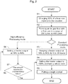
- a predetermined amount as an initial charging amount of silicon raw material M is charged into the crucible 3 (Step S1 in Fig. 2 ).
- This amount is to be equal to or less than 30% of a total amount of silicon raw material enough for growing one single crystal silicon. The reason is to reduce contamination to the silicon raw material M as much as possible because CO gas generates in the furnace at the initial stage of heating the crucible, as described later.
- the heater controller 9 operates by a command from the CPU 8b, based on a program stored in the memory device 8a, to supply power to the heater 4 to heat the crucible 3, and melting operation of the silicon raw material M is started (Step S3 in Fig. 2 ).
- an output W of the heater 4 is kept in a range from 15% to 50% of the output (100%) of the heater output that is necessary to melt the silicon raw material M completely.
- heating at relatively low temperature in a range from 250 degrees C to 750 degrees C causes to generate CO gas from carbon-made members, such as the heater 4, the crucible 3 and the thermal insulator 13, and can result to evacuate the CO gas, that is, to replace it with Ar.
- a low output state of the heater 4 is kept for a predetermined period; that is, a time range from 3 hours to 20 hours (In a standard mode case in Fig. 2 ) .
- a predetermined period that is, a time range from 3 hours to 20 hours (In a standard mode case in Fig. 2 ) .
- the heater output is less than 15% of the output of the heater output needed to melt the silicon raw material M completely, it is not desirable because the temperature of the carbon-made members fails to rise enough to release CO gas completely.
- the heater output is more than 50% of the output of the heater output needed to melt the silicon raw material M completely, it is not desirable because, when the temperature of the silicon raw material M rises before the temperature of the carbon-made members in the furnace rises to a predetermined value, then the temperature enhances the surface reaction of the CO gas with the silicon raw material, and the concentration of carbon in the silicon melt increases.
- step S3 in Fig.2 keeping the output of the heater 4 to be low for a period of 3 hours to 20 hours enables CO gas generated from the carbon-made members in the furnace to be exhausted to the outside.
- the flow rate of Ar gas in the furnace is in a range from 200 L/min to 400 L/min.
- the Ar gas flow is as much as possible.
- the heater controller 9 is controlled by a command from the CPU 8b to switch the heater output W of the heater 4 to an output necessary to melt the silicon raw material M completely (Step S4 in Fig. 2 ).
- This procedure makes the whole silicon raw material M in the crucible 3 melt.
- the silicon melt When the silicon raw material M gets melted, the silicon melt generates SiO gas, and CO gas is generated by a reaction of the carbon-made members in the furnace, such as the heater 4, the crucible 3 and the thermal insulator 13, with the SiO gas.
- the generation of CO gas gives little influences because it occurs at a downstream side of the exhausting pump 19 rather than the silicon raw material M from a viewpoint of a gas flowing path.
- holding time of keeping the heater output low is a predetermined value, that is, 3 hours to 20 hours.
- utilization of a gas analyzer 7 shown in Fig. 1 , a quadrupole mass spectrometer for example, for monitoring the amount of CO gas may allow an improvement of production efficiency (High efficiency mode case in Fig. 2 ).
- an output W of the heater 4 is kept in a range from 15% to 50% of the output (100%) of the heater output that is necessary to melt the silicon raw material M completely (Step S6 in Fig. 2 ).
- the CPU 8b monitors the amount of CO gas in the furnace based on results of analysis with the gas analyzer 7. After due to the heating process of S3 the concentration has risen to a peak value and turned to decrease, then the CPU 8b detects a timing when the concentration decreases by 30% or more of the peak value (Step S7 in Fig. 2 ).
- the reason why the timing is when the concentration decreases by 30% or more of the peak value is because there is a case the amount of the CO gas may increase again after the concentration has risen to a peak value and turned to decrease, and variation in analysis is also taken into account.
- the heater controller 9 is controlled by a command from the CPU 8b to switch the heater output W of the heater 4 to an output necessary to melt the silicon raw material M completely (Step S4 in Fig. 2 ).
- the initial charged weight of the silicon raw material is equal to or less than 30% of the final charged weight.
- Reducing the charged silicon raw material enables to prevent formation of a film containing Si-C bonding on the surface of silicon raw material and an increase of carbon concentration in the silicon melt.
- the timing of additional charging of the silicon raw material M is preferably determined after the step S3 or S7; the output of the heater 4 is set to 15% to 50% of the output necessary to melt the silicon raw material M completely and to be kept for in a range from 3 hours to 20 hours.
- a step of additionally charging the silicon raw material to the crucible 3 is preferably executed before the output of the heater 4 is set to the necessary output for melting the silicon raw material M completely and the silicon raw material melt to form a silicon melt (Step S4).
- Step S5 in Fig. 2 After the whole silicon raw material is melted and a silicon melt is formed, processing is shifted to a single crystal pulling step (Step S5 in Fig. 2 ).
- the elevation device 11a and the wire-reel rotation controller 12 start to operate by a command from the CPU 8b and the height of the rotating crucible 3 is adjusted and the wire winding mechanism 5a starts to operate to move the wire 5b downward.
- a seed crystal attached to the distal end of the wire 5b comes into contact with the silicon melt and the tip portion of the seed crystal dipped into the melt.
- necking is carried out to form a neck part having a diameter of 3 mm to 6 mm and a length of 100 mm to 400 mm.
- a condition of parameters such as electric power supply to the heater 4, a pulling speed of a single crystal that is typically a few millimeters/min, is adjusted by commands from the CPU 8b, then pulling processes are carried out in turn, such as a crowning process to enlarge the diameter of the crystal to a straight body diameter, a process to form a straight body that is to be a product, and a process to form a tail part in which the diameter of the crystal is reduced from the straight body diameter.
- CO gas generated from the carbon-made members in the furnace is released under the condition that an output of the heater 4 is kept in a range from 15% to 50% of the output necessary to completely melt the silicon raw material M, and then evacuated. After that the output of the heater is raised to form a silicon melt in the crucible 3.
- This process can suppress reaction of CO gas generated from the carbon-made members with the surface of the silicon raw material and resultantly formation of a film containing Si-C bonding on the surface of the silicon raw material M. Namely, an increase of carbon concentration in the silicon melt due to the intake of the film containing Si-C bonding into the melt can be suppressed.
- the inert gas introduced to the furnace is Ar, but not restricted to Ar.
- a production method of single crystal silicon according to the present invention will be describe based on the embodiment. Following experiments were carried out based on the embodiment.
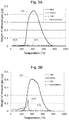
- Sample 1 is a piece of thermal insulator having a dimension of 10 mm x 10 mm x 5 mm and Sample 2 is a piece of graphite made by a cold isostatic pressing method (CIP) having a dimension of 10 mm x 10 mm x 5 mm; both of the samples are materials used in a furnace.
- CIP cold isostatic pressing method
- the inside of the furnace was heated up to 1000 degrees C at a temperature rising speed of 10 degrees/min and He gas was flown at a flow rate of 50 mL/min at an atmospheric pressure.
- both the sample 1 and sample 2 generated larger amount of generated CO gas when the temperature inside the furnace was between 250 degrees C and 750 degrees C.
- the weight of the generated CO gas is heavier than the weight of the generated CO 2 gas; it is confirmed that CO gas gives greater influence to the concentration of carbon in the single crystal silicon.
- a silicon melt by melting a silicon raw material typically requires about 1800 degrees C at the maximum temperature in the furnace. There usually is a temperature distribution inside the furnace; the temperature in the vicinity of the heater as a heat source in Fig. 1 is the highest.
- the heater output is rapidly raised to an output necessary to melt the silicon raw material completely, the vicinity of the heater and the silicon raw material in the crucible become a high temperature state but carbon-made members disposed away from the heater are still in a low temperature state.
- the silicon raw material becomes at a rather high temperature, and the reaction between the silicon raw material and the generated CO gas is promoted thereby.
- the heater output is set to an output that can maintain the temperature of the carbon-made members disposed away from the heater in a range from 250 degree C to 750 degrees C and the holding time is set in a range from 3 hours to 20 hours.
- the heater output enabling to maintain the temperature of the carbon-made members in a range from 250 degree C to 750 degrees C corresponds to 15% to 50% of the heater output necessary to melt the silicon raw material completely.
- the carbon concentration was a high value of 1.5 ⁇ 10 15 atoms/cm 3 . This is thought to be because, with a low heater output of a value of 10%, the temperature of the carbon-made members in the furnace did not rise enough and CO gas was not released completely.
- the carbon concentration was a high value of 2.0 ⁇ 10 15 atoms/cm 3 . This is thought to be because, due to a high heater output of a value of 60%, before the temperature of the carbon-made members in the furnace rose, the temperature of the silicon raw material rose up and promoted the reaction between the surface of the silicon raw material and CO gas; this resulted in an increase of carbon concentration in the silicon melt.
- the carbon concentration was a high value of 1.5 ⁇ 10 15 atoms/cm 3 . This is thought to be because the holding time too short, that is, 2 hours, the CO gas was not completely released.
- the carbon concentration was a high value of 1.8 ⁇ 10 15 atoms/cm 3 . This is thought to be because the Ar flow rate was too low, 100 L/min, CO gas was not effectively evacuated; this caused to increase carbon concentration due to reaction of CO gas in the furnace.
- a silicon melt was formed with a heater output of 100 kW after the crucible with a heater output of 30 kW was kept for 3 hours; the heater output was 30% of a heater output of 100 kW necessary to melt silicon raw material necessary for growing a single crystal with a diameter of 150 mm.
- the flow rate of Ar in the furnace was set to be 150 L/min in the embodiment 7 and 120 L/min in the embodiment 8.
- a silicon melt was formed with a heater output of 100 kW from the beginning of crucible heating.
- the flow rate of Ar in the furnace was set to be 150 L/min in the comparative example 5, and 120 L/min in the comparative example 6.
- Graphs in Fig. 4 show the results of the embodiments 7 and 8, and examples 5 and 8.
- every measured carbon concentration is plotted on the vertical axis in a unit of 10 15 atoms/cm 3 for every condition, which is placed on the horizontal axis as a group, of embodiments 7 and 8 and comparative examples 5 and 6.
- the present invention can greatly reduce carbon concentration in the crystals in comparison to conventional methods.
Landscapes
- Chemical & Material Sciences (AREA)
- Engineering & Computer Science (AREA)
- Crystallography & Structural Chemistry (AREA)
- Materials Engineering (AREA)
- Metallurgy (AREA)
- Organic Chemistry (AREA)
- Crystals, And After-Treatments Of Crystals (AREA)
Applications Claiming Priority (1)
| Application Number | Priority Date | Filing Date | Title |
|---|---|---|---|
| JP2018007053A JP7049119B2 (ja) | 2018-01-19 | 2018-01-19 | シリコン単結晶の製造方法 |
Publications (2)
| Publication Number | Publication Date |
|---|---|
| EP3514264A1 true EP3514264A1 (de) | 2019-07-24 |
| EP3514264B1 EP3514264B1 (de) | 2024-02-21 |
Family
ID=65010668
Family Applications (1)
| Application Number | Title | Priority Date | Filing Date |
|---|---|---|---|
| EP19150932.2A Active EP3514264B1 (de) | 2018-01-19 | 2019-01-09 | Herstellungsverfahren eines einkristallsiliciums |
Country Status (5)
| Country | Link |
|---|---|
| EP (1) | EP3514264B1 (de) |
| JP (1) | JP7049119B2 (de) |
| KR (1) | KR102165349B1 (de) |
| CN (1) | CN110055582B (de) |
| TW (1) | TWI689634B (de) |
Cited By (2)
| Publication number | Priority date | Publication date | Assignee | Title |
|---|---|---|---|---|
| CN114235737A (zh) * | 2021-12-22 | 2022-03-25 | 新疆大全新能源股份有限公司 | 一种多晶硅中碳含量的检测方法 |
| WO2022140812A1 (de) | 2020-12-29 | 2022-07-07 | Fametec Gmbh | Verfahren zur herstellung eines einkristalls |
Citations (6)
| Publication number | Priority date | Publication date | Assignee | Title |
|---|---|---|---|---|
| JPS5615946B2 (de) | 1973-08-27 | 1981-04-13 | ||
| JPH0383887A (ja) * | 1989-08-28 | 1991-04-09 | Toshiba Corp | 半導体単結晶の引上方法及びその装置 |
| JPH0789789A (ja) | 1993-09-20 | 1995-04-04 | Fujitsu Ltd | Si結晶、結晶成長方法および結晶成長装置 |
| JP2635456B2 (ja) | 1991-06-28 | 1997-07-30 | 信越半導体株式会社 | シリコン単結晶の引上方法 |
| EP1774068A1 (de) * | 2004-08-05 | 2007-04-18 | Vladimir Iljich Amosov | Verfahren zum ziehen von einkristallen aus einer schmelze |
| US20090235861A1 (en) * | 2008-03-18 | 2009-09-24 | Sumco Corporation | Carbon-doped single crystal manufacturing method |
Family Cites Families (7)
| Publication number | Priority date | Publication date | Assignee | Title |
|---|---|---|---|---|
| DE19638563C2 (de) * | 1996-09-20 | 1999-07-08 | Karlsruhe Forschzent | Verfahren zum Ziehen von Einkristallen |
| JP4716331B2 (ja) * | 2006-09-29 | 2011-07-06 | コバレントマテリアル株式会社 | 単結晶の製造方法 |
| EP2650405A3 (de) * | 2008-11-05 | 2014-02-26 | MEMC Singapore Pte. Ltd. | Verfahren zur Herstellung einer Schmelze von Siliciumpulver zum Ziehen von Siliciumkristallen |
| JP5052493B2 (ja) * | 2008-12-29 | 2012-10-17 | ジャパンスーパークォーツ株式会社 | シリコン単結晶の製造方法 |
| JP5577726B2 (ja) * | 2010-02-08 | 2014-08-27 | 株式会社Sumco | シリコン原料の溶解方法および供給装置 |
| CN103255469A (zh) * | 2013-06-03 | 2013-08-21 | 英利能源(中国)有限公司 | 石墨加热器、石墨电极和降低硅片中碳含量的方法 |
| JP5921498B2 (ja) * | 2013-07-12 | 2016-05-24 | グローバルウェーハズ・ジャパン株式会社 | シリコン単結晶の製造方法 |
-
2018
- 2018-01-19 JP JP2018007053A patent/JP7049119B2/ja active Active
- 2018-11-23 TW TW107141867A patent/TWI689634B/zh active
-
2019
- 2019-01-09 EP EP19150932.2A patent/EP3514264B1/de active Active
- 2019-01-14 KR KR1020190004694A patent/KR102165349B1/ko active Active
- 2019-01-18 CN CN201910048771.0A patent/CN110055582B/zh active Active
Patent Citations (6)
| Publication number | Priority date | Publication date | Assignee | Title |
|---|---|---|---|---|
| JPS5615946B2 (de) | 1973-08-27 | 1981-04-13 | ||
| JPH0383887A (ja) * | 1989-08-28 | 1991-04-09 | Toshiba Corp | 半導体単結晶の引上方法及びその装置 |
| JP2635456B2 (ja) | 1991-06-28 | 1997-07-30 | 信越半導体株式会社 | シリコン単結晶の引上方法 |
| JPH0789789A (ja) | 1993-09-20 | 1995-04-04 | Fujitsu Ltd | Si結晶、結晶成長方法および結晶成長装置 |
| EP1774068A1 (de) * | 2004-08-05 | 2007-04-18 | Vladimir Iljich Amosov | Verfahren zum ziehen von einkristallen aus einer schmelze |
| US20090235861A1 (en) * | 2008-03-18 | 2009-09-24 | Sumco Corporation | Carbon-doped single crystal manufacturing method |
Cited By (2)
| Publication number | Priority date | Publication date | Assignee | Title |
|---|---|---|---|---|
| WO2022140812A1 (de) | 2020-12-29 | 2022-07-07 | Fametec Gmbh | Verfahren zur herstellung eines einkristalls |
| CN114235737A (zh) * | 2021-12-22 | 2022-03-25 | 新疆大全新能源股份有限公司 | 一种多晶硅中碳含量的检测方法 |
Also Published As
| Publication number | Publication date |
|---|---|
| TW201940754A (zh) | 2019-10-16 |
| CN110055582A (zh) | 2019-07-26 |
| EP3514264B1 (de) | 2024-02-21 |
| JP2019123656A (ja) | 2019-07-25 |
| KR20190088886A (ko) | 2019-07-29 |
| TWI689634B (zh) | 2020-04-01 |
| KR102165349B1 (ko) | 2020-10-13 |
| CN110055582B (zh) | 2021-07-16 |
| JP7049119B2 (ja) | 2022-04-06 |
Similar Documents
| Publication | Publication Date | Title |
|---|---|---|
| US9758899B2 (en) | Manufacturing method of silicon single crystal having low-resistivity electrical characteristics | |
| US8580032B2 (en) | Method for manufacturing single crystal | |
| JP5176101B2 (ja) | シリコン単結晶の製造方法および装置並びにシリコン単結晶インゴット | |
| US10494734B2 (en) | Method for producing silicon single crystals | |
| TWI519684B (zh) | 在控制壓力下使用氦氣之高溫製程改良 | |
| KR102054186B1 (ko) | 실리콘 단결정 제조방법 | |
| CN110678585B (zh) | 单晶硅锭的制造方法及单晶硅培育装置 | |
| TWI888636B (zh) | 用於生長晶體之方法 | |
| US20130153836A1 (en) | Method of producing silicon carbide single crystal, silicon carbide single crystal, and silicon carbide single crystal substrate | |
| EP3514264B1 (de) | Herstellungsverfahren eines einkristallsiliciums | |
| JP5437565B2 (ja) | 半導体単結晶の製造装置 | |
| JP4780705B2 (ja) | 単結晶半導体の製造装置および製造方法 | |
| JP4396505B2 (ja) | シリコン単結晶の製造方法 | |
| WO2017017893A1 (ja) | シリコン単結晶育成装置 | |
| US20200199776A1 (en) | Method for producing silicon single crystal | |
| JP2007223814A (ja) | 単結晶半導体の製造方法 | |
| US20250207294A1 (en) | Manufacturing method of silicon single crystal | |
| CN120225734A (zh) | 用于控制晶体生长过程期间气体掺杂剂蒸发速率的系统及方法 | |
| JPH07237992A (ja) | 化合物半導体単結晶の製造方法 | |
| JP2002128593A (ja) | シリコンウェーハの製造方法及びその方法により製造されたシリコンウェーハ |
Legal Events
| Date | Code | Title | Description |
|---|---|---|---|
| PUAI | Public reference made under article 153(3) epc to a published international application that has entered the european phase |
Free format text: ORIGINAL CODE: 0009012 |
|
| STAA | Information on the status of an ep patent application or granted ep patent |
Free format text: STATUS: THE APPLICATION HAS BEEN PUBLISHED |
|
| AK | Designated contracting states |
Kind code of ref document: A1 Designated state(s): AL AT BE BG CH CY CZ DE DK EE ES FI FR GB GR HR HU IE IS IT LI LT LU LV MC MK MT NL NO PL PT RO RS SE SI SK SM TR |
|
| AX | Request for extension of the european patent |
Extension state: BA ME |
|
| STAA | Information on the status of an ep patent application or granted ep patent |
Free format text: STATUS: REQUEST FOR EXAMINATION WAS MADE |
|
| STAA | Information on the status of an ep patent application or granted ep patent |
Free format text: STATUS: EXAMINATION IS IN PROGRESS |
|
| 17P | Request for examination filed |
Effective date: 20200117 |
|
| RBV | Designated contracting states (corrected) |
Designated state(s): AL AT BE BG CH CY CZ DE DK EE ES FI FR GB GR HR HU IE IS IT LI LT LU LV MC MK MT NL NO PL PT RO RS SE SI SK SM TR |
|
| 17Q | First examination report despatched |
Effective date: 20200227 |
|
| GRAP | Despatch of communication of intention to grant a patent |
Free format text: ORIGINAL CODE: EPIDOSNIGR1 |
|
| STAA | Information on the status of an ep patent application or granted ep patent |
Free format text: STATUS: GRANT OF PATENT IS INTENDED |
|
| INTG | Intention to grant announced |
Effective date: 20230914 |
|
| RIN1 | Information on inventor provided before grant (corrected) |
Inventor name: ABE, YOSHIAKI Inventor name: NAGAI, YUTA Inventor name: TSUBOTA, HIROYUKI Inventor name: MATSUMURA, HISASHI |
|
| GRAS | Grant fee paid |
Free format text: ORIGINAL CODE: EPIDOSNIGR3 |
|
| GRAA | (expected) grant |
Free format text: ORIGINAL CODE: 0009210 |
|
| STAA | Information on the status of an ep patent application or granted ep patent |
Free format text: STATUS: THE PATENT HAS BEEN GRANTED |
|
| AK | Designated contracting states |
Kind code of ref document: B1 Designated state(s): AL AT BE BG CH CY CZ DE DK EE ES FI FR GB GR HR HU IE IS IT LI LT LU LV MC MK MT NL NO PL PT RO RS SE SI SK SM TR |
|
| REG | Reference to a national code |
Ref country code: GB Ref legal event code: FG4D |
|
| REG | Reference to a national code |
Ref country code: CH Ref legal event code: EP |
|
| REG | Reference to a national code |
Ref country code: DE Ref legal event code: R096 Ref document number: 602019046772 Country of ref document: DE |
|
| REG | Reference to a national code |
Ref country code: IE Ref legal event code: FG4D |
|
| REG | Reference to a national code |
Ref country code: LT Ref legal event code: MG9D |
|
| REG | Reference to a national code |
Ref country code: NL Ref legal event code: MP Effective date: 20240221 |
|
| PG25 | Lapsed in a contracting state [announced via postgrant information from national office to epo] |
Ref country code: IS Free format text: LAPSE BECAUSE OF FAILURE TO SUBMIT A TRANSLATION OF THE DESCRIPTION OR TO PAY THE FEE WITHIN THE PRESCRIBED TIME-LIMIT Effective date: 20240621 |
|
| PG25 | Lapsed in a contracting state [announced via postgrant information from national office to epo] |
Ref country code: LT Free format text: LAPSE BECAUSE OF FAILURE TO SUBMIT A TRANSLATION OF THE DESCRIPTION OR TO PAY THE FEE WITHIN THE PRESCRIBED TIME-LIMIT Effective date: 20240221 |
|
| PG25 | Lapsed in a contracting state [announced via postgrant information from national office to epo] |
Ref country code: GR Free format text: LAPSE BECAUSE OF FAILURE TO SUBMIT A TRANSLATION OF THE DESCRIPTION OR TO PAY THE FEE WITHIN THE PRESCRIBED TIME-LIMIT Effective date: 20240522 |
|
| REG | Reference to a national code |
Ref country code: AT Ref legal event code: MK05 Ref document number: 1659180 Country of ref document: AT Kind code of ref document: T Effective date: 20240221 |
|
| PG25 | Lapsed in a contracting state [announced via postgrant information from national office to epo] |
Ref country code: RS Free format text: LAPSE BECAUSE OF FAILURE TO SUBMIT A TRANSLATION OF THE DESCRIPTION OR TO PAY THE FEE WITHIN THE PRESCRIBED TIME-LIMIT Effective date: 20240521 Ref country code: HR Free format text: LAPSE BECAUSE OF FAILURE TO SUBMIT A TRANSLATION OF THE DESCRIPTION OR TO PAY THE FEE WITHIN THE PRESCRIBED TIME-LIMIT Effective date: 20240221 Ref country code: NL Free format text: LAPSE BECAUSE OF FAILURE TO SUBMIT A TRANSLATION OF THE DESCRIPTION OR TO PAY THE FEE WITHIN THE PRESCRIBED TIME-LIMIT Effective date: 20240221 |
|
| PG25 | Lapsed in a contracting state [announced via postgrant information from national office to epo] |
Ref country code: ES Free format text: LAPSE BECAUSE OF FAILURE TO SUBMIT A TRANSLATION OF THE DESCRIPTION OR TO PAY THE FEE WITHIN THE PRESCRIBED TIME-LIMIT Effective date: 20240221 |
|
| PG25 | Lapsed in a contracting state [announced via postgrant information from national office to epo] |
Ref country code: AT Free format text: LAPSE BECAUSE OF FAILURE TO SUBMIT A TRANSLATION OF THE DESCRIPTION OR TO PAY THE FEE WITHIN THE PRESCRIBED TIME-LIMIT Effective date: 20240221 |
|
| PG25 | Lapsed in a contracting state [announced via postgrant information from national office to epo] |
Ref country code: RS Free format text: LAPSE BECAUSE OF FAILURE TO SUBMIT A TRANSLATION OF THE DESCRIPTION OR TO PAY THE FEE WITHIN THE PRESCRIBED TIME-LIMIT Effective date: 20240521 Ref country code: NO Free format text: LAPSE BECAUSE OF FAILURE TO SUBMIT A TRANSLATION OF THE DESCRIPTION OR TO PAY THE FEE WITHIN THE PRESCRIBED TIME-LIMIT Effective date: 20240521 Ref country code: NL Free format text: LAPSE BECAUSE OF FAILURE TO SUBMIT A TRANSLATION OF THE DESCRIPTION OR TO PAY THE FEE WITHIN THE PRESCRIBED TIME-LIMIT Effective date: 20240221 Ref country code: LT Free format text: LAPSE BECAUSE OF FAILURE TO SUBMIT A TRANSLATION OF THE DESCRIPTION OR TO PAY THE FEE WITHIN THE PRESCRIBED TIME-LIMIT Effective date: 20240221 Ref country code: IS Free format text: LAPSE BECAUSE OF FAILURE TO SUBMIT A TRANSLATION OF THE DESCRIPTION OR TO PAY THE FEE WITHIN THE PRESCRIBED TIME-LIMIT Effective date: 20240621 Ref country code: HR Free format text: LAPSE BECAUSE OF FAILURE TO SUBMIT A TRANSLATION OF THE DESCRIPTION OR TO PAY THE FEE WITHIN THE PRESCRIBED TIME-LIMIT Effective date: 20240221 Ref country code: GR Free format text: LAPSE BECAUSE OF FAILURE TO SUBMIT A TRANSLATION OF THE DESCRIPTION OR TO PAY THE FEE WITHIN THE PRESCRIBED TIME-LIMIT Effective date: 20240522 Ref country code: FI Free format text: LAPSE BECAUSE OF FAILURE TO SUBMIT A TRANSLATION OF THE DESCRIPTION OR TO PAY THE FEE WITHIN THE PRESCRIBED TIME-LIMIT Effective date: 20240221 Ref country code: ES Free format text: LAPSE BECAUSE OF FAILURE TO SUBMIT A TRANSLATION OF THE DESCRIPTION OR TO PAY THE FEE WITHIN THE PRESCRIBED TIME-LIMIT Effective date: 20240221 Ref country code: BG Free format text: LAPSE BECAUSE OF FAILURE TO SUBMIT A TRANSLATION OF THE DESCRIPTION OR TO PAY THE FEE WITHIN THE PRESCRIBED TIME-LIMIT Effective date: 20240221 Ref country code: AT Free format text: LAPSE BECAUSE OF FAILURE TO SUBMIT A TRANSLATION OF THE DESCRIPTION OR TO PAY THE FEE WITHIN THE PRESCRIBED TIME-LIMIT Effective date: 20240221 |
|
| PG25 | Lapsed in a contracting state [announced via postgrant information from national office to epo] |
Ref country code: PL Free format text: LAPSE BECAUSE OF FAILURE TO SUBMIT A TRANSLATION OF THE DESCRIPTION OR TO PAY THE FEE WITHIN THE PRESCRIBED TIME-LIMIT Effective date: 20240221 Ref country code: PT Free format text: LAPSE BECAUSE OF FAILURE TO SUBMIT A TRANSLATION OF THE DESCRIPTION OR TO PAY THE FEE WITHIN THE PRESCRIBED TIME-LIMIT Effective date: 20240621 |
|
| PG25 | Lapsed in a contracting state [announced via postgrant information from national office to epo] |
Ref country code: SE Free format text: LAPSE BECAUSE OF FAILURE TO SUBMIT A TRANSLATION OF THE DESCRIPTION OR TO PAY THE FEE WITHIN THE PRESCRIBED TIME-LIMIT Effective date: 20240221 Ref country code: PT Free format text: LAPSE BECAUSE OF FAILURE TO SUBMIT A TRANSLATION OF THE DESCRIPTION OR TO PAY THE FEE WITHIN THE PRESCRIBED TIME-LIMIT Effective date: 20240621 Ref country code: PL Free format text: LAPSE BECAUSE OF FAILURE TO SUBMIT A TRANSLATION OF THE DESCRIPTION OR TO PAY THE FEE WITHIN THE PRESCRIBED TIME-LIMIT Effective date: 20240221 Ref country code: LV Free format text: LAPSE BECAUSE OF FAILURE TO SUBMIT A TRANSLATION OF THE DESCRIPTION OR TO PAY THE FEE WITHIN THE PRESCRIBED TIME-LIMIT Effective date: 20240221 |
|
| PG25 | Lapsed in a contracting state [announced via postgrant information from national office to epo] |
Ref country code: DK Free format text: LAPSE BECAUSE OF FAILURE TO SUBMIT A TRANSLATION OF THE DESCRIPTION OR TO PAY THE FEE WITHIN THE PRESCRIBED TIME-LIMIT Effective date: 20240221 |
|
| PG25 | Lapsed in a contracting state [announced via postgrant information from national office to epo] |
Ref country code: SM Free format text: LAPSE BECAUSE OF FAILURE TO SUBMIT A TRANSLATION OF THE DESCRIPTION OR TO PAY THE FEE WITHIN THE PRESCRIBED TIME-LIMIT Effective date: 20240221 |
|
| PG25 | Lapsed in a contracting state [announced via postgrant information from national office to epo] |
Ref country code: CZ Free format text: LAPSE BECAUSE OF FAILURE TO SUBMIT A TRANSLATION OF THE DESCRIPTION OR TO PAY THE FEE WITHIN THE PRESCRIBED TIME-LIMIT Effective date: 20240221 Ref country code: EE Free format text: LAPSE BECAUSE OF FAILURE TO SUBMIT A TRANSLATION OF THE DESCRIPTION OR TO PAY THE FEE WITHIN THE PRESCRIBED TIME-LIMIT Effective date: 20240221 |
|
| PG25 | Lapsed in a contracting state [announced via postgrant information from national office to epo] |
Ref country code: SK Free format text: LAPSE BECAUSE OF FAILURE TO SUBMIT A TRANSLATION OF THE DESCRIPTION OR TO PAY THE FEE WITHIN THE PRESCRIBED TIME-LIMIT Effective date: 20240221 |
|
| PG25 | Lapsed in a contracting state [announced via postgrant information from national office to epo] |
Ref country code: SM Free format text: LAPSE BECAUSE OF FAILURE TO SUBMIT A TRANSLATION OF THE DESCRIPTION OR TO PAY THE FEE WITHIN THE PRESCRIBED TIME-LIMIT Effective date: 20240221 Ref country code: SK Free format text: LAPSE BECAUSE OF FAILURE TO SUBMIT A TRANSLATION OF THE DESCRIPTION OR TO PAY THE FEE WITHIN THE PRESCRIBED TIME-LIMIT Effective date: 20240221 Ref country code: RO Free format text: LAPSE BECAUSE OF FAILURE TO SUBMIT A TRANSLATION OF THE DESCRIPTION OR TO PAY THE FEE WITHIN THE PRESCRIBED TIME-LIMIT Effective date: 20240221 Ref country code: EE Free format text: LAPSE BECAUSE OF FAILURE TO SUBMIT A TRANSLATION OF THE DESCRIPTION OR TO PAY THE FEE WITHIN THE PRESCRIBED TIME-LIMIT Effective date: 20240221 Ref country code: DK Free format text: LAPSE BECAUSE OF FAILURE TO SUBMIT A TRANSLATION OF THE DESCRIPTION OR TO PAY THE FEE WITHIN THE PRESCRIBED TIME-LIMIT Effective date: 20240221 Ref country code: CZ Free format text: LAPSE BECAUSE OF FAILURE TO SUBMIT A TRANSLATION OF THE DESCRIPTION OR TO PAY THE FEE WITHIN THE PRESCRIBED TIME-LIMIT Effective date: 20240221 |
|
| REG | Reference to a national code |
Ref country code: DE Ref legal event code: R097 Ref document number: 602019046772 Country of ref document: DE |
|
| PG25 | Lapsed in a contracting state [announced via postgrant information from national office to epo] |
Ref country code: IT Free format text: LAPSE BECAUSE OF FAILURE TO SUBMIT A TRANSLATION OF THE DESCRIPTION OR TO PAY THE FEE WITHIN THE PRESCRIBED TIME-LIMIT Effective date: 20240221 |
|
| PLBE | No opposition filed within time limit |
Free format text: ORIGINAL CODE: 0009261 |
|
| STAA | Information on the status of an ep patent application or granted ep patent |
Free format text: STATUS: NO OPPOSITION FILED WITHIN TIME LIMIT |
|
| PG25 | Lapsed in a contracting state [announced via postgrant information from national office to epo] |
Ref country code: IT Free format text: LAPSE BECAUSE OF FAILURE TO SUBMIT A TRANSLATION OF THE DESCRIPTION OR TO PAY THE FEE WITHIN THE PRESCRIBED TIME-LIMIT Effective date: 20240221 |
|
| 26N | No opposition filed |
Effective date: 20241122 |
|
| PG25 | Lapsed in a contracting state [announced via postgrant information from national office to epo] |
Ref country code: SI Free format text: LAPSE BECAUSE OF FAILURE TO SUBMIT A TRANSLATION OF THE DESCRIPTION OR TO PAY THE FEE WITHIN THE PRESCRIBED TIME-LIMIT Effective date: 20240221 |
|
| REG | Reference to a national code |
Ref country code: CH Ref legal event code: PL |
|
| PG25 | Lapsed in a contracting state [announced via postgrant information from national office to epo] |
Ref country code: LU Free format text: LAPSE BECAUSE OF NON-PAYMENT OF DUE FEES Effective date: 20250109 Ref country code: MC Free format text: LAPSE BECAUSE OF FAILURE TO SUBMIT A TRANSLATION OF THE DESCRIPTION OR TO PAY THE FEE WITHIN THE PRESCRIBED TIME-LIMIT Effective date: 20240221 |
|
| GBPC | Gb: european patent ceased through non-payment of renewal fee |
Effective date: 20250109 |
|
| PG25 | Lapsed in a contracting state [announced via postgrant information from national office to epo] |
Ref country code: GB Free format text: LAPSE BECAUSE OF NON-PAYMENT OF DUE FEES Effective date: 20250109 Ref country code: BE Free format text: LAPSE BECAUSE OF NON-PAYMENT OF DUE FEES Effective date: 20250131 |
|
| PG25 | Lapsed in a contracting state [announced via postgrant information from national office to epo] |
Ref country code: FR Free format text: LAPSE BECAUSE OF NON-PAYMENT OF DUE FEES Effective date: 20250131 |
|
| PG25 | Lapsed in a contracting state [announced via postgrant information from national office to epo] |
Ref country code: CH Free format text: LAPSE BECAUSE OF NON-PAYMENT OF DUE FEES Effective date: 20250131 |
|
| REG | Reference to a national code |
Ref country code: BE Ref legal event code: MM Effective date: 20250131 |
|
| PG25 | Lapsed in a contracting state [announced via postgrant information from national office to epo] |
Ref country code: IE Free format text: LAPSE BECAUSE OF NON-PAYMENT OF DUE FEES Effective date: 20250109 |
|
| PGFP | Annual fee paid to national office [announced via postgrant information from national office to epo] |
Ref country code: DE Payment date: 20260122 Year of fee payment: 8 |
|
| PG25 | Lapsed in a contracting state [announced via postgrant information from national office to epo] |
Ref country code: CY Free format text: LAPSE BECAUSE OF FAILURE TO SUBMIT A TRANSLATION OF THE DESCRIPTION OR TO PAY THE FEE WITHIN THE PRESCRIBED TIME-LIMIT Effective date: 20240221 |
|
| PG25 | Lapsed in a contracting state [announced via postgrant information from national office to epo] |
Ref country code: TR Free format text: LAPSE BECAUSE OF FAILURE TO SUBMIT A TRANSLATION OF THE DESCRIPTION OR TO PAY THE FEE WITHIN THE PRESCRIBED TIME-LIMIT Effective date: 20240221 |