EP3514810A1 - Verbesserte anschlussaustrittsanordnung in einer elektrischen vorrichtung - Google Patents
Verbesserte anschlussaustrittsanordnung in einer elektrischen vorrichtung Download PDFInfo
- Publication number
- EP3514810A1 EP3514810A1 EP18152531.2A EP18152531A EP3514810A1 EP 3514810 A1 EP3514810 A1 EP 3514810A1 EP 18152531 A EP18152531 A EP 18152531A EP 3514810 A1 EP3514810 A1 EP 3514810A1
- Authority
- EP
- European Patent Office
- Prior art keywords
- bushing
- conductor
- electrical device
- winding element
- axis
- Prior art date
- Legal status (The legal status is an assumption and is not a legal conclusion. Google has not performed a legal analysis and makes no representation as to the accuracy of the status listed.)
- Withdrawn
Links
Images




Classifications
-
- H—ELECTRICITY
- H01—ELECTRIC ELEMENTS
- H01F—MAGNETS; INDUCTANCES; TRANSFORMERS; SELECTION OF MATERIALS FOR THEIR MAGNETIC PROPERTIES
- H01F27/00—Details of transformers or inductances, in general
- H01F27/28—Coils; Windings; Conductive connections
- H01F27/2823—Wires
- H01F27/2828—Construction of conductive connections, of leads
-
- H—ELECTRICITY
- H01—ELECTRIC ELEMENTS
- H01F—MAGNETS; INDUCTANCES; TRANSFORMERS; SELECTION OF MATERIALS FOR THEIR MAGNETIC PROPERTIES
- H01F27/00—Details of transformers or inductances, in general
- H01F27/02—Casings
- H01F27/04—Leading of conductors or axles through casings, e.g. for tap-changing arrangements
Definitions
- the present invention relates to an electrical device having a housing, a core, at least one winding element surrounding parts of the core, at least one bushing positioned adjacent to the winding element, and a conductor.
- Such an electrical device is known to a person skilled in the art.
- a commonly known electrical device is, for example, a high voltage power transformer or a reactor.
- FIG 1A illustrates a sectional view of an active part of an electrical device 100, of the state of the art, as mentioned above.
- the electrical device 100 comprises a tank 101 housing a core 102 positioned therein.
- a winding element 103 partially surrounds the core 102.
- a bushing 104 is positioned partially inside the tank 101 and adjacent to the winding element 103.
- the electrical device 100 also comprises a lead exit 105 positioned inside the tank 101.
- the lead exit 105 is a current carrying connection from a winding element 103 to another winding element 103, or to a tap changer, or to exit terminals, that is, bushings 104. In order to withstand operational conditions, lead exits 105 are required to be properly insulated, supported and cooled.
- FIG 1B illustrates an enlarged view of a portion of the electrical device 100, marked "X" in FIG 1A showing the lead exit 105 of the state of the art.
- a lead exit 105 comprises a conductor 105A carrying current there within.
- the conductor 105A is typically covered in insulation 105B such as cellulose based insulating material.
- This insulation 105B is further covered by one or more insulating barriers 105C.
- the insulating barriers 105C are separated by oil gaps there between.
- the insulating barriers 105C increase dielectric strength of the oil gaps by separating them into smaller channels.
- Quantity of these insulating barriers 105C and distances there between, are dependent on a dielectric stress exerted on the conductor 105A and its surrounding areas, during operation of the electrical device 100.
- the dielectric stress is a function of parameters comprising voltage, geometry of the conductor 105A, positioning of the conductor 105A, insulating materials used, distance of the conductor 105A with respect to surrounding elements such as the tank 101, the bushing 104, the winding element 103, etc.
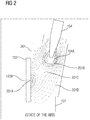
- FIG 2 illustrates a sectional view of the state of the art electrical device 100, illustrated in FIG 1A , showing a contour plot 201 of various voltage fields created between the winding element 103 and the bushing 104 during operation of the electrical device 100.
- the contour plot 201 is represented without considering the lead exit 105 positioned between the winding element 103 and the bushing 104.
- a voltage field 201A around a mid-portion 103A of the winding element 103 and a voltage field 201B around a lower end 104A of the bushing 104, are both high voltage fields.
- a voltage field 201C of the contour plot 201, around the high voltage fields 201A and 201B is at a voltage lower than that of the voltage fields 201A and 201B.
- a voltage field 201D of the contour plot 201 is at a lowest voltage compared to that of the voltage fields 201A, 201B, and 201C.
- Each of the contour lines of the contour plot 201 are illustrated by dotted lines, the continuity of which decreases as a function of voltage that the contour lines represent, that is, an increase in discontinuity of the contour lines of the contour plot 201 indicates a gradual decrease in the voltages of the voltage fields 201A, 201B, 201C, and 201D.
- a conductor 105A illustrated in FIGS 1A-1B when placed in the voltage fields 201A, 201B, 201C, and 201D having varying voltages therein, experiences high levels of dielectric stress as opposed to a conductor 105A positioned in a voltage field having a uniform voltage.
- the dielectric stress is high, higher is the quantity of insulation barriers 105C required to be mounted on the conductor 105A in order to withstand the operational conditions.
- costs of the lead exits 105 typically increase with the quantity of insulation barriers 105C employed as a result of material costs, associated component costs such as oil gap spacers, etc., and associated labour costs of installing the insulation barriers 105C.
- the electrical device disclosed in the present invention achieves the aforementioned object, in that the winding element and the bushing are positioned with respect to one another, so as to create an equipotential voltage field there between during operation of the electrical device.
- an electrical device having a housing, a core positioned inside the housing, at least one winding element, at least one bushing, and a conductor.
- the housing for example, refers to a tank of a high voltage transformer.
- the winding element partially surrounds the core.
- the bushing is positioned at least partially inside the housing and adjacent to the winding element.
- adjacent refers to geometric proximity of the bushing with respect to the winding element.
- the winding element and the bushing are positioned with respect to one another so as to create an equipotential voltage field there between during operation of the electrical device.
- operation refers to all normal and abnormal operating conditions, for example, testing of the electrical device.
- equivalentpotential voltage field refers to a region in space having a uniform potential spread across the region. For example, when a voltage measurement probe is positioned at various points along such an electric field, the voltage measured at each of the points is nearly equal.
- the equipotential field encompasses an area surrounding the winding element, an area surrounding the bushing, and an area there between, such that the electric field has a continuous uniform potential there within.
- the winding element is positioned along a first axis and the bushing is positioned along a second axis such that the first axis and the second axis have a predefined angle of inclination there between.
- the second axis, along which the bushing is positioned is inclined with respect to the first axis, along which the winding element is positioned. That is, the first axis is aligned vertically and the second axis is aligned at an inclination with respect to the vertical.
- the predefined angle of inclination between the first axis and the second axis is in a range of about 5 degrees to about 30 degrees.
- the bushing is positioned along the second axis such that a lower end of the bushing is in close proximity with a mid-portion of the winding element so as to create the equipotential field.
- a distance between the lower end of the bushing and the mid-portion of the winding elements is in a range of about 300mm to about 800mm.
- a voltage between the bushing and the winding element, that is, in the equipotential field is equal to a voltage at the bushing and/or a voltage at the winding element.
- the term "equal” is not to be limited to mathematical equality but extended to a range of variation of the voltage between the bushing and the winding element with respect to the voltages at the bushing and/or the winding elements. This range is about 0% to about -20%.
- the voltages at the bushing, at the winding element, and in the equipotential field, are based on an operational rating of the electrical device, for example, a voltage range of 200kV to 1200kV, for high voltage transformers and reactors.
- the conductor is positioned inside the housing and connects the winding element to the bushing.
- the conductor provides a current carrying path between the winding element and another conductor enclosed in the bushing.
- the conductor is positioned between the bushing and the winding element such that the conductor is accommodated within the equipotential voltage field.
- the conductor is entirely accommodated within the equipotential voltage field.
- the conductor is near completely accommodated within the equipotential voltage field.
- the conductor is configured of a developed length lesser than or equal to about 1000 mm.
- the conductor is configured to have a first insulating element positioned thereon.
- the first insulating element is configured to cover the conductor surface, for example, by wrapping it, tightly winding it, etc., over the conductor.
- a thickness of the first insulating element lies in a range of about 0 mm to about 20 mm.
- the conductor is configured to have subsequent insulating barriers positioned around the first insulating element. The subsequent insulating barriers are positioned such that there is a predefined gap there between for allowing oil to be stored therein. Spacers may be employed to maintain these oil gaps in the subsequent insulating barriers.
- the first insulating element and the subsequent insulating barriers are configured of cellulose based materials.
- the first insulating element and the subsequent insulating barriers are configured based on one or more stresses that the conductor experiences in the equipotential voltage field. For example, a thickness of the first insulating element, a number of the subsequent insulating barriers, a thickness of each of the subsequent insulating barriers, gaps between the subsequent insulating barriers, etc., is configured based on the stresses.
- the stresses comprise, for example, dielectric stress.
- the stresses and thereby the number of subsequent insulating barriers is a function of the variation of the voltage between the bushing and the winding element with respect to the voltages at the bushing and the winding element. For example, when the voltage variation is more than about 20%, the stresses increase, thereby increasing the number of subsequent insulating barriers.
- the dielectric stress is below a design threshold, for example, 4.5kV/mm, the number of subsequent insulating barriers required is 0.
- a number, of the subsequent insulating barriers is in a range of about 0 to 2.
- a method for assembling the aforementioned electrical device comprising a housing, a core, at least one winding element, at least one bushing, and a conductor.
- the method comprises positioning the bushing along a first axis and the winding element along a second axis such that the first axis and the second axis have a predefined angle of inclination there between and so as to create an equipotential voltage field there between, during operation of the electrical device.
- the method comprises positioning the conductor between the bushing and the winding element such that the conductor is accommodated within the equipotential voltage field.
- the method comprises, determining one or more stresses exerted on the conductor in the equipotential voltage field and configuring a first insulating element to be positioned on the conductor, and subsequent insulating barriers to be positioned on the first insulating element, based on the stresses.
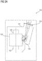
- FIG 3A illustrates an active part of a transformer as an embodiment of an electrical device 100, according to the present invention.
- the active part of the electrical device 100 comprises a housing 101, a core 102, at least one winding element 103, at least one bushing 104, and a lead exit 105 providing a current carrying path between the winding element 103 and the bushing 104.
- FIG 3B illustrates an enlarged view of a portion of the electrical device 100, marked "Y" in FIG 3A showing an equipotential voltage field 301 created between the winding element 103 and the bushing 104 and accommodating a conductor 105A therewithin, according to the present invention.
- the equipotential field 301 is represented by contour lines 301A, 301B, 301C, and 301D each representing a different voltage in the equipotential voltage field.
- the contour line 301A represents a uniform equipotential voltage field of the highest voltage compared to that represented by the contour line 301D.
- the equipotential field 301 is created by arranging the bushing 104 and the winding element 103 in close proximity with one another.
- the bushing is aligned along the axis A-A' and the winding element is aligned along the axis B-B', such that the axes A-A' and B-B' converge at a predefined angle of inclination ⁇ , such that, there is an equipotential field 301 created between a mid-portion 103A of the winding element 103 and a lower end 104A of the bushing 104, while maintaining clearances there between as per standard design practices.
- the lead exit 105 is positioned such that it is entirely accommodated in the equipotential voltage field 301.
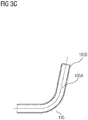
- FIG 3C illustrates an enlarged view of a lead exit 105 of an electrical device 100 shown in FIG 3A , according to the present invention.
- the lead exit 105 that is entirely positioned within the equipotential field 301 shown in FIG 3B , experiences negligible dielectric stress due to which insulation requirements of the lead exit 105 decrease substantially, thereby eliminating need of subsequent insulating barriers 105C, shown in FIG 1B .
- the lead exit 105 comprises a conductor 105A having a first insulating element 105B of a thickness approximately less than 20mm. This insulation in the lead exit 105 is sufficient to maintain the dielectric stresses on an outermost surface of the lead exit 105, within a design limit, for example, of 4.5kV/mm.
- FIG 4 illustrates a process flowchart 400 of an exemplary method of assembling the electrical device 100 shown in FIG 3A , in accordance with an embodiment of the present invention.
- the electrical device 100 comprises a housing 101, a core 102, at least one winding element 103, at least one bushing 104, and a lead exit 105 as shown in FIG 3A .
- the method comprises positioning the bushing 104, along a first axis A-A', and the winding element 103, along a second axis B-B', such that, a lower end 104A of the bushing 104 is positioned proximal to a mid-portion 103A of the winding element 103.
- This positioning is such that the first axis A-A' and the second axis B-B' have a predefined angle of inclination ⁇ there between so as to create an equipotential voltage field 301 there between, as shown in FIG 3B , during operation of the electrical device 100.
- the method comprises positioning the lead exit 105 comprising a conductor 105A, between the bushing 104 and the winding element 103 such that the conductor 105A is accommodated within the equipotential voltage field 301.
- the method comprises determining one or more stresses exerted on the conductor 105A positioned in the equipotential voltage field 301. For example, using electrostatic field calculations, dielectric stresses exerted on the conductor 105A are measured.
- the method comprises configuring a first insulating element 105B to be positioned on the conductor 105A, and subsequent insulating barriers 105C to be positioned around the first insulating element 105B, based on the one or more stresses.
- the method comprises comparing the dielectric stress with its design limit of 4.5kV/mm. If the dielectric stress is less than 4.5kV/mm then the first insulating element 105B of a thickness less than 20mm is configured and there is no requirement to position any subsequent insulating barriers 105C.
- the subsequent insulating barriers 105C required range from about 0 to 2, with a thickness of the first insulating element ranging from about 0mm to about 20mm.
Landscapes
- Engineering & Computer Science (AREA)
- Power Engineering (AREA)
- Housings And Mounting Of Transformers (AREA)
Priority Applications (1)
| Application Number | Priority Date | Filing Date | Title |
|---|---|---|---|
| EP18152531.2A EP3514810A1 (de) | 2018-01-19 | 2018-01-19 | Verbesserte anschlussaustrittsanordnung in einer elektrischen vorrichtung |
Applications Claiming Priority (1)
| Application Number | Priority Date | Filing Date | Title |
|---|---|---|---|
| EP18152531.2A EP3514810A1 (de) | 2018-01-19 | 2018-01-19 | Verbesserte anschlussaustrittsanordnung in einer elektrischen vorrichtung |
Publications (1)
| Publication Number | Publication Date |
|---|---|
| EP3514810A1 true EP3514810A1 (de) | 2019-07-24 |
Family
ID=61074300
Family Applications (1)
| Application Number | Title | Priority Date | Filing Date |
|---|---|---|---|
| EP18152531.2A Withdrawn EP3514810A1 (de) | 2018-01-19 | 2018-01-19 | Verbesserte anschlussaustrittsanordnung in einer elektrischen vorrichtung |
Country Status (1)
| Country | Link |
|---|---|
| EP (1) | EP3514810A1 (de) |
Citations (6)
| Publication number | Priority date | Publication date | Assignee | Title |
|---|---|---|---|---|
| DE904078C (de) * | 1942-04-15 | 1954-02-15 | Aeg | Grosstransformator, insbesondere Wandertransformator |
| JPS5642313A (en) * | 1979-09-14 | 1981-04-20 | Fuji Electric Co Ltd | Shielding for high-tension bushing of oil-immersed induction apparatus |
| JPS6046013A (ja) * | 1983-08-24 | 1985-03-12 | Hitachi Ltd | 電気機器 |
| JPS60193316A (ja) * | 1984-03-15 | 1985-10-01 | Toshiba Corp | 直流油入電気機器 |
| JPS60193315A (ja) * | 1984-03-15 | 1985-10-01 | Toshiba Corp | 直流油入電気機器 |
| DE19530163A1 (de) * | 1995-08-03 | 1997-02-06 | Aeg Tro Transformatoren Gmbh | Hochspannungsausleitungs- und durchführungsanordnung für Transformatoren und Drosselspulen |
-
2018
- 2018-01-19 EP EP18152531.2A patent/EP3514810A1/de not_active Withdrawn
Patent Citations (6)
| Publication number | Priority date | Publication date | Assignee | Title |
|---|---|---|---|---|
| DE904078C (de) * | 1942-04-15 | 1954-02-15 | Aeg | Grosstransformator, insbesondere Wandertransformator |
| JPS5642313A (en) * | 1979-09-14 | 1981-04-20 | Fuji Electric Co Ltd | Shielding for high-tension bushing of oil-immersed induction apparatus |
| JPS6046013A (ja) * | 1983-08-24 | 1985-03-12 | Hitachi Ltd | 電気機器 |
| JPS60193316A (ja) * | 1984-03-15 | 1985-10-01 | Toshiba Corp | 直流油入電気機器 |
| JPS60193315A (ja) * | 1984-03-15 | 1985-10-01 | Toshiba Corp | 直流油入電気機器 |
| DE19530163A1 (de) * | 1995-08-03 | 1997-02-06 | Aeg Tro Transformatoren Gmbh | Hochspannungsausleitungs- und durchführungsanordnung für Transformatoren und Drosselspulen |
Similar Documents
| Publication | Publication Date | Title |
|---|---|---|
| JP5859142B2 (ja) | ガス絶縁電気機器 | |
| EP2234137B1 (de) | Vakuumschaltanlage | |
| CZ387998A3 (cs) | Transformátor/reaktor | |
| JP6595428B2 (ja) | 避雷器 | |
| US8764467B2 (en) | External connector for solid insulated load break switchgear | |
| EP0053363B1 (de) | Durchführung für gasisolierte, elektrische Geräte | |
| CN101405819A (zh) | 用于电气屏蔽设备的连接元件 | |
| KR20180049848A (ko) | 고전압 퓨즈 제조 공정 및 이를 통해 제조된 고전압 퓨즈 | |
| EP2528071B1 (de) | Hochspannungsanordnung mit Isolationsstruktur | |
| US4404423A (en) | Three-phase gas insulated bus | |
| KR102682995B1 (ko) | 탭 어셈블리를 갖는 부싱 | |
| JP3744721B2 (ja) | 可撓性導体及び可撓性接続部材 | |
| US11962133B2 (en) | Air insulated switch with very compact gap length | |
| US3980804A (en) | High tension coaxial cable with end structure for preventing glow discharges | |
| EP3776614B1 (de) | Adapter für einen kondensator | |
| KR20110035852A (ko) | 개폐기용 전극 및 진공 개폐기와, 개폐기용 전극 또는 진공 개폐기의 제조방법 | |
| JPH09292435A (ja) | 耐電圧試験保護装置 | |
| KR101522271B1 (ko) | 개폐기의 부분방전 시험장치 | |
| KR102152703B1 (ko) | 고전압 전력기기용 전류 도입선 구조 | |
| WO2016027494A1 (ja) | 電力用開閉器 | |
| CN114391104A (zh) | 用于测量功率开关装置中的导体处的电压电势的测量装置和相应的功率开关装置 | |
| US20260031553A1 (en) | Pmj with different diameters and rubber unit with different diameters for connection of ultra-high voltage cable with different diameters | |
| EP4618127A1 (de) | Strombegrenzungssicherungsanordnung, transformatoranordnung mit strombegrenzungssicherungsanordnung und abschirmanordnung zum elektrischen und mechanischen abschirmen einer strombegrenzungssicherung | |
| JP5635473B2 (ja) | X線装置及び変圧器 | |
| CN112868077B (zh) | 用于在高压技术下调低电位的装置和方法 |
Legal Events
| Date | Code | Title | Description |
|---|---|---|---|
| PUAI | Public reference made under article 153(3) epc to a published international application that has entered the european phase |
Free format text: ORIGINAL CODE: 0009012 |
|
| STAA | Information on the status of an ep patent application or granted ep patent |
Free format text: STATUS: THE APPLICATION HAS BEEN PUBLISHED |
|
| AK | Designated contracting states |
Kind code of ref document: A1 Designated state(s): AL AT BE BG CH CY CZ DE DK EE ES FI FR GB GR HR HU IE IS IT LI LT LU LV MC MK MT NL NO PL PT RO RS SE SI SK SM TR |
|
| AX | Request for extension of the european patent |
Extension state: BA ME |
|
| STAA | Information on the status of an ep patent application or granted ep patent |
Free format text: STATUS: REQUEST FOR EXAMINATION WAS MADE |
|
| 17P | Request for examination filed |
Effective date: 20200113 |
|
| RBV | Designated contracting states (corrected) |
Designated state(s): AL AT BE BG CH CY CZ DE DK EE ES FI FR GB GR HR HU IE IS IT LI LT LU LV MC MK MT NL NO PL PT RO RS SE SI SK SM TR |
|
| RAP1 | Party data changed (applicant data changed or rights of an application transferred) |
Owner name: SIEMENS ENERGY GLOBAL GMBH & CO. KG |
|
| STAA | Information on the status of an ep patent application or granted ep patent |
Free format text: STATUS: EXAMINATION IS IN PROGRESS |
|
| 17Q | First examination report despatched |
Effective date: 20211110 |
|
| STAA | Information on the status of an ep patent application or granted ep patent |
Free format text: STATUS: THE APPLICATION IS DEEMED TO BE WITHDRAWN |
|
| 18D | Application deemed to be withdrawn |
Effective date: 20220322 |