EP3518347A1 - Steckverbinder mit verriegelnder sicherungshaube - Google Patents
Steckverbinder mit verriegelnder sicherungshaube Download PDFInfo
- Publication number
- EP3518347A1 EP3518347A1 EP18200624.7A EP18200624A EP3518347A1 EP 3518347 A1 EP3518347 A1 EP 3518347A1 EP 18200624 A EP18200624 A EP 18200624A EP 3518347 A1 EP3518347 A1 EP 3518347A1
- Authority
- EP
- European Patent Office
- Prior art keywords
- connector
- latching
- contact carrier
- circuit board
- locking
- Prior art date
- Legal status (The legal status is an assumption and is not a legal conclusion. Google has not performed a legal analysis and makes no representation as to the accuracy of the status listed.)
- Granted
Links
Images









Classifications
-
- H—ELECTRICITY
- H01—ELECTRIC ELEMENTS
- H01R—ELECTRICALLY-CONDUCTIVE CONNECTIONS; STRUCTURAL ASSOCIATIONS OF A PLURALITY OF MUTUALLY-INSULATED ELECTRICAL CONNECTING ELEMENTS; COUPLING DEVICES; CURRENT COLLECTORS
- H01R12/00—Structural associations of a plurality of mutually-insulated electrical connecting elements, specially adapted for printed circuits, e.g. printed circuit boards [PCB], flat or ribbon cables, or like generally planar structures, e.g. terminal strips, terminal blocks; Coupling devices specially adapted for printed circuits, flat or ribbon cables, or like generally planar structures; Terminals specially adapted for contact with, or insertion into, printed circuits, flat or ribbon cables, or like generally planar structures
- H01R12/70—Coupling devices
- H01R12/7005—Guiding, mounting, polarizing or locking means; Extractors
- H01R12/7011—Locking or fixing a connector to a PCB
- H01R12/7017—Snap means
- H01R12/7029—Snap means not integral with the coupling device
-
- H—ELECTRICITY
- H01—ELECTRIC ELEMENTS
- H01R—ELECTRICALLY-CONDUCTIVE CONNECTIONS; STRUCTURAL ASSOCIATIONS OF A PLURALITY OF MUTUALLY-INSULATED ELECTRICAL CONNECTING ELEMENTS; COUPLING DEVICES; CURRENT COLLECTORS
- H01R12/00—Structural associations of a plurality of mutually-insulated electrical connecting elements, specially adapted for printed circuits, e.g. printed circuit boards [PCB], flat or ribbon cables, or like generally planar structures, e.g. terminal strips, terminal blocks; Coupling devices specially adapted for printed circuits, flat or ribbon cables, or like generally planar structures; Terminals specially adapted for contact with, or insertion into, printed circuits, flat or ribbon cables, or like generally planar structures
- H01R12/50—Fixed connections
- H01R12/51—Fixed connections for rigid printed circuits or like structures
- H01R12/515—Terminal blocks providing connections to wires or cables
-
- H—ELECTRICITY
- H01—ELECTRIC ELEMENTS
- H01R—ELECTRICALLY-CONDUCTIVE CONNECTIONS; STRUCTURAL ASSOCIATIONS OF A PLURALITY OF MUTUALLY-INSULATED ELECTRICAL CONNECTING ELEMENTS; COUPLING DEVICES; CURRENT COLLECTORS
- H01R12/00—Structural associations of a plurality of mutually-insulated electrical connecting elements, specially adapted for printed circuits, e.g. printed circuit boards [PCB], flat or ribbon cables, or like generally planar structures, e.g. terminal strips, terminal blocks; Coupling devices specially adapted for printed circuits, flat or ribbon cables, or like generally planar structures; Terminals specially adapted for contact with, or insertion into, printed circuits, flat or ribbon cables, or like generally planar structures
- H01R12/70—Coupling devices
- H01R12/71—Coupling devices for rigid printing circuits or like structures
- H01R12/712—Coupling devices for rigid printing circuits or like structures co-operating with the surface of the printed circuit or with a coupling device exclusively provided on the surface of the printed circuit
-
- H—ELECTRICITY
- H01—ELECTRIC ELEMENTS
- H01R—ELECTRICALLY-CONDUCTIVE CONNECTIONS; STRUCTURAL ASSOCIATIONS OF A PLURALITY OF MUTUALLY-INSULATED ELECTRICAL CONNECTING ELEMENTS; COUPLING DEVICES; CURRENT COLLECTORS
- H01R13/00—Details of coupling devices of the kinds covered by groups H01R12/70 or H01R24/00 - H01R33/00
- H01R13/46—Bases; Cases
- H01R13/516—Means for holding or embracing insulating body, e.g. casing, hoods
-
- H—ELECTRICITY
- H01—ELECTRIC ELEMENTS
- H01R—ELECTRICALLY-CONDUCTIVE CONNECTIONS; STRUCTURAL ASSOCIATIONS OF A PLURALITY OF MUTUALLY-INSULATED ELECTRICAL CONNECTING ELEMENTS; COUPLING DEVICES; CURRENT COLLECTORS
- H01R12/00—Structural associations of a plurality of mutually-insulated electrical connecting elements, specially adapted for printed circuits, e.g. printed circuit boards [PCB], flat or ribbon cables, or like generally planar structures, e.g. terminal strips, terminal blocks; Coupling devices specially adapted for printed circuits, flat or ribbon cables, or like generally planar structures; Terminals specially adapted for contact with, or insertion into, printed circuits, flat or ribbon cables, or like generally planar structures
- H01R12/70—Coupling devices
- H01R12/7005—Guiding, mounting, polarizing or locking means; Extractors
- H01R12/7011—Locking or fixing a connector to a PCB
- H01R12/7052—Locking or fixing a connector to a PCB characterised by the locating members
-
- H—ELECTRICITY
- H01—ELECTRIC ELEMENTS
- H01R—ELECTRICALLY-CONDUCTIVE CONNECTIONS; STRUCTURAL ASSOCIATIONS OF A PLURALITY OF MUTUALLY-INSULATED ELECTRICAL CONNECTING ELEMENTS; COUPLING DEVICES; CURRENT COLLECTORS
- H01R13/00—Details of coupling devices of the kinds covered by groups H01R12/70 or H01R24/00 - H01R33/00
- H01R13/64—Means for preventing incorrect coupling
- H01R13/645—Means for preventing incorrect coupling by exchangeable elements on case or base
- H01R13/6456—Means for preventing incorrect coupling by exchangeable elements on case or base comprising keying elements at different positions along the periphery of the connector
Definitions
- the invention relates to a connector, in particular direct connector for contacting contact openings of a printed circuit board, with a contact carrier, which may have coding, in particular coding pins and a reverse polarity, in particular in the form of Polungsvorsprüngen with formed by the contact carrier conductor insertion channels for receiving connecting conductors and contact recesses for receiving plug contacts, with a securing hood, which surrounds the contact carrier, wherein the contact carrier in the safety hood in the insertion direction of the connector displaceable between a mounting position and a pre-assembly is displaced and with a connector holding the circuit board primary fuse, which is part of the fuse hood, wherein the primary fuse is displaceable from a latch position to a release position.
- a contact carrier which may have coding, in particular coding pins and a reverse polarity, in particular in the form of Polungsvorsprüngen with formed by the contact carrier conductor insertion channels for receiving connecting conductors and contact recesses for receiving plug
- the connectors serve to make contact with a connecting conductor to a printed circuit board by means of plug contacts.
- the connectors can be designed as a direct connector. These direct connectors have plug contacts whose conductor sections are contacted directly by the printed circuit board. These direct connectors are provided with plug contacts for specially shaped printed circuit boards, which have openings for this purpose, the inner peripheral surface is provided with an electrical layer. This electrically conductive layer of the printed circuit board comes into direct contact with the contact fingers of the plug contacts.
- connectors which have a safety hood.
- the fuse cover surrounds the contact carrier of the connector outer circumference, wherein the Contact carrier is movably arranged in the safety hood to be able to be moved from a pre-assembly to a mounting position.
- the contact carrier which carries the plug contacts, is moved from the pre-assembly in the mounting position.
- the fuse cover surrounding the contact carrier then securely holds the connector to the circuit board.
- the primary fuse secures the connector to the circuit board and protects the contact between the connector and the circuit board against unintentional release. Furthermore, the primary fuse serves to protect against increased tensile forces, which are applied by the connecting conductors. The primary fuse thus ensures a secure and permanent contact.
- the primary fuse forms at least one locking element, which cooperates with cutouts in the circuit board to arrange the connector to the circuit board.
- These locking elements have latching means which engage under the circuit board.
- Connectors are subjected to constant miniaturization, with the requirements for securing the connector to the circuit board remain at least constant.
- the object of the invention is to provide a connector whose design ensures an optimized and secure fixing of the primary fuse to the circuit board.
- the invention is solved by a connector having the features of claim 1, in particular its characterizing feature, after which the contact carrier holds in its mounting position within the safety hood, the primary fuse in its locked position.
- the main advantage of the invention is that the primary fuse of the fuse cover is held by the contact carrier located in the mounting position on the circuit board in the locked position.
- the primary fuse is thus blocked against displacement into the release position and removal of the connector from the circuit board is not possible nondestructive.
- a connector fixed in this way on the printed circuit board can thus withstand higher loads and can therefore also be used in environments with increased vibration without detaching from the printed circuit board.
- the primary fuse comprises at least one locking arm arranged on the locking arm, which extends in the plugging direction.
- the locking arm arranged on the securing arm engages under the printed circuit board in order to arrange the plug connector on the printed circuit board.
- the contact carrier is arranged in its mounting position in that space in which the latching arm is to shift to take the release position and thus blocks the displacement movement of the latching arm in the release position.
- the primary fuse has at least two mutually opposite latching arms, wherein the space is arranged for the arrangement of the contact carrier in its mounting position between the latching arms.
- the primary fuse comprises at least two paired juxtaposed latching arms whose locking members have different locking geometries.
- the latching member of the first latching arm has a latching surface which engages under the printed circuit board and which is oriented substantially orthogonally to the plugging direction of the plug connector.
- the locking surface is thus aligned approximately parallel to the underside of the circuit board.
- the connector is thus secured against tensile force.
- the holding force of the first locking arm is up to 60 Newton.
- the latching member of the second latching arm has a circuit board at least teiluntermatide latching surface which is formed starting from the latching arm in the direction of insertion drop.
- the locking arm initially serves to compensate for tolerances between the contact carrier of the connector and the circuit board.
- the printed circuit board is completely or at least partially underlaid by the sloping latching surface and, in addition to the first latching surface, provides the plug connector with support on the printed circuit board.
- the angle between the sloping locking surface with the circuit board encloses an angle of 20 ° and thus allows a tolerance compensation of up to 10% of the nominal thickness of the circuit board.
- the safety hood has two oppositely arranged and oriented in the insertion direction Rastarmpaare.
- the latching arms of different Rastarmpaare with locking members of the same geometry are diagonally opposite each other.
- each latching arms has a release cam, which serves the return displacement of the locking member in the space of the release position to separate the connector from the circuit board, wherein the contact carrier is displaced in the pre-assembly.
- the contact carrier must be in the preassembly position prior to disconnecting the connector from the circuit board to avoid blocking the latching arms of the primary fuse.
- release cams of the latching arms are optional and therefore not a mandatory feature of the latching arms.
- a connector according to the invention is provided overall with the reference numeral 10.
- FIGS. 1 to 14 a first embodiment of the connector 10 is disclosed.
- a second embodiment is in the FIGS. 15 to 18 shown.
- Identical or equivalent components are named with identical reference numerals and terms. Unless otherwise specified, the comments on an embodiment apply mutatis mutandis to the alternative embodiment.
- Fig. 1 is shown in addition to the connector 10 with a contact carrier 11 and a secondary fuse 26, a printed circuit board 19.
- the connector 10 has the contact carrier 11 which forms a housing 13 for plug contacts 12.
- the housing 13 of the connector 10 has the contact carrier 11 which forms a housing 13 for plug contacts 12.
- Contact carrier 11 is provided with conductor insertion channels 14, which serve to receive connecting leads, not shown here. These are electrically connected via insulation displacement forks 48 with the plug contacts 12.
- the plug contacts 12 form the contact fingers 49, which engage under the contact opening 36 of a printed circuit board 19 as soon as the plug connector 10 is arranged on the printed circuit board 19, such as in Fig. 11 shown.
- the housing 13 is provided with contact recesses 15, in which the plug contacts 12 are inserted.
- the housing 13 carries on its outer surface a plurality of Kodierstatte 16, which project the connector 10 in the insertion direction and the connector 10 on the circuit board 19 with a corresponding coding, in particular in the form of Codierbohrungen 37, assign.
- the housing 13 has on its front side 20 snap hooks 21, by means of which a plurality of connectors 10 can be arranged for confectioning purposes together.
- the housing 13 forms contours for receiving 23 of latching hooks 21, by means of which more connectors 10 can be arranged on the contact carrier 11.
- the contact carrier 11 is equipped with a reverse polarity fuse 18.
- the polarity reversal fuse 18 is intended to prevent a short-circuiting contacting of the plug contacts 12 with the contact openings 36 of the printed circuit board 19.
- the reverse polarity fuse 18 is formed by three of the underside of the contact carrier 11 springing Polungsvorsprüngen 56, such as in Fig. 6 shown. In this case, two of the polarity projections 56 are formed on the contact carrier 11 with respect to the paper plane right, whereas only one Polungsvorspung 56 is formed on the left with respect to the paper plane.
- the housing 13 of the contact carrier 11 is plug-in direction parallel with a bore 24 passes.
- This bore 24 has a first notch 25A and a second notch 25B.
- the second notch 25B is an optional and non-mandatory feature of the bore 24.
- the bore 24 serves to receive the secondary fuse 26, in particular in the form of a latching pin 27.
- the latching pin 27 has a head portion 28 and a pin-like base body 29.
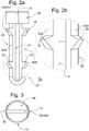
- the Fig. 2a shows the locking pin 27 in side view.
- the outer circumference of the pin-like base body 29 of the locking pin 27 is partially surrounded by mounting load projections 47 and locking latch projections 33.
- the mounting loader protrusions 47 is used for pre-assembly of the locking pin 27 on the contact carrier 11.
- the locking latch projections 33 engage under the circuit board 19 and hold the connector 10 to the circuit board 19th
- the locking latch projections 33 which increases in Fig. 2b are shown are threaded portion-like and serve the bracing of the contact carrier 11 on the circuit board 19. At the same time the thread pitch also allows compensation of board tolerances.
- the pin-like base body 29 of the locking pin 27 has a slot 41 which is bounded by a first side wall 40A and a second side wall 40B.
- the slit 41 permits a diameter-reducing backward displacement of the side walls 40A and 40B supporting the latch detent projections 33.
- the rib 31 is shown in the head region 28, the rib 31 is shown. This cooperates with the first or the second notch 25A, 25B of the bore 24 (see Fig. 1 . Fig. 5 ). This rib 31 cooperates depending on the locking position of the latching pin 27 with the first or second notch 25A, 25B and thus holds the latching pin 27 or its locking latch projections 33 in the latch or Entriegel ein the secondary fuse 26th
- the rib 31 and the head portion 28 of the locking pin 27 are in the Fig. 3 shown.
- the head portion 28 forms a groove 30A, which serves to receive a tool, not shown here, and thus displaces the locking pin 27 in the locking or unlocking position.
- a screwdriver can be introduced, by means of which the locking pin 27 can rotate in the bore 24 by 90 °.
- the Fig. 4 shows the circuit board 19 from above.
- the printed circuit board 19 forms the contact openings 36 for receiving the plug contacts 12 of the contact carrier 11.
- the circuit board 19 has a formed in the middle of the circuit board 19 opening 39 with a keyhole-like contour. This contour is subdivided into a stalk section 58 and a beard section 38.
- the stalk section 58 serves to receive the pin-like basic body 29 of the latching pin 27.
- the beard section 38 serves to receive a coding pin 16 of the contact carrier 11. Adjacent to this beard section 38 are two coding holes 37 in FIG the printed circuit board 19 is formed, which serve to receive the remaining coding pins 16 of the contact carrier 11.
- the printed circuit board 19 Adjacent to the opening 39, the printed circuit board 19 has a first and a second slot 35A, 35B.
- These elongated holes 35A and 35B have portions which cooperate on the one hand with a primary fuse 17 and on the other hand with the polarity projections 56 of the polarity reversal fuse 18.
- the elongated hole 35A cooperates with the primary fuse 17 and with a polarity projection 56.
- the elongate hole 35B cooperates with the primary fuse 17 and with two polarity projections 56 and is accordingly longer than the elongate hole 35A. An incorrect positioning of the connector 10 on the circuit board 19 is thus excluded.
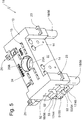
- the primary fuse 17 is for example in the Fig. 5 to 7 represented and serves the arrangement of the contact carrier 11 on the circuit board 19.
- the primary fuse 17 is formed by two Rastarmpresen.
- Each pair of latching arms has a first latching arm 44 and a second latching arm 45.
- the latching arms 44, 45 each originate from a latching arm root 52 which is remote from the free end and which is arranged on the contact carrier 11.
- the latching arms 44, 45 each have a release cam 53, which serve the return displacement of the latching arms 44, 45 in a release position to disconnect the connector 10 of printed circuit board 19, if a corresponding pressure is applied here, the release cam an optional and thus no mandatory feature of the locking arms 44, 45 are.
- the latching arms 44, 45 have at their free end latching members 50 and 51, which have different locking surfaces 54 and 55.
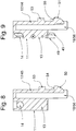
- the first locking member 50 of the second locking arm 45 is shown.
- the first latching element 50 of the second latching arm 45 forms a latching surface 54 which engages under the printed circuit board 19.
- This latching surface 54 is aligned substantially orthogonal to the insertion direction of the connector, that is approximately parallel to the bottom 46 of the circuit board 19, as shown for example in the Fig. 11 and 13 can be seen.
- the connector 10 is thus secured against a tensile force that can be applied, for example, by the connection conductors, not shown, secured.
- the latching surface 54 of the first latching member 50 allows a holding force of up to 60 Newtons.
- the second locking member 51 of the locking arm 44 has a latching surface 55, which is formed starting from the first latching arm 44 in the insertion direction sloping.
- the latching surface 55 serves to compensate for tolerances between the contact carrier 11 and the circuit board 19.
- the arranged on the circuit board 19 locking arms 44 are for example in the Fig. 11 and 13 shown.
- Printed circuit boards 19 with minimum thickness fully engages below the sloping latching surface 55, so that the surface origin located near the first latching arm 44 provides the plug connector 10 with support on the printed circuit board 19 in addition to the latching surface 54.
- Circuit boards 19 with a maximum strength engages below the sloping locking surface 55 only with its end facing away from the origin, which provides the connector 10 complementary to the locking surface 54 hold.
- a unter the locking surface 55 instead.
- the sloping locking surface 55 with the bottom 46 of the circuit board 19 forms an angle of 20 ° and thus allows a tolerance compensation of up to 10% of the nominal thickness of the circuit board 19.
- the sloping locking surface 55 contributes to the anchoring of the connector 10th at the circuit board 19 at. However, the tensile load that can be compensated by them is low due to the sloping locking surface 55.
- the latching arms 44, 45 rush to the contact carrier 11 and are arranged parallel to each other.
- the connector 10 has two Rastarmplanen which are arranged on opposite sides of the connector 10.
- the locking members 50 and 51 of the same locking geometry are opposite each other diagonally on the contact carrier 11.
- the example of Figure 11 can be seen that the latching member 51 of the left with respect to the paper plane Rastarmpaares front, the locking member 50, however, is arranged behind.
- the right-hand pair of latching arms with respect to the plane of the paper has a front latching element 50, whereas the latching element 51 is located at the rear. In this way, the aforementioned diagonality is ensured.
- the secondary fuse 26 is mounted in unlocking position and in top view ( Fig. 10 ) and from below ( Fig. 11 ).
- the unlocking position is indicated here by the groove 30A pointing to the word "release".
- Another form of optical display is possible.
- the rib 31 of the head region 28 of the latching pin 27 cooperates with the first notch 25A associated with the term "release”.
- the rib 31 and the first notch 25A hold the detent pin 27 in the unlocked position.
- An independent turning of the locking pin 27 or by vibration is not possible.
- the secondary fuse 26 is merely mounted in the blade section 58 of the opening 39 in such a way that the locking latch projections 33 of the latching pin 27 do not engage under the printed circuit board 19.
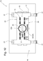
- the locking pin 27 is displaced in the locked position.
- the rotatably mounted locking pin 27 allows the contact carrier 11 to be clamped to the circuit board 19 by the locking pin 27 is rotated at mounted on the circuit board 19 connector 10 from the unlocking into the locked position.
- the latching pin 27 is mounted in the locking position so in the stalk area 58 of the opening 39 that the locking latch projections 33 of the locking pin 27 engage under the circuit board 19 and the contact carrier 11 by the threaded portion-like configuration of the locking latch projections 33 clamped to the circuit board 19.
- the locking pin 27 may already be in the locked position when placed on the printed circuit board 19. Then the locking latch projections 33 run on the edge of the opening 39.
- the vertically arranged in the locking pin 27 slot 41 allows the continuation of the detent pin a resilient rearward displacement of the locking latch projections 33 of the detent pin 27 so that they swap through the opening 39 and thus engage the circuit board 19.
- this connector 10 has a securing hood 60.
- the securing hood 60 surrounds the contact carrier 11 on the outside, the contact carrier 11 being movably arranged in the securing hood 60.
- the contact carrier 11 has plug-in direction parallel locking pin 61, which lead the contact carrier 11 and position it in the safety cap 60 in the pre-assembly.
- the contact carrier 11 forms latching profiles 63 and latching grooves 66, which lead the contact carrier 11 in the direction of insertion and corresponding to the front or mounting position of the contact carrier 11 in the Collet 60 cooperate with locking webs 65 of the safety cover 60.
- the contact carrier 11 has latching tabs 62 which originate from the housing 13 on the respective short sides of the contact carrier 11.
- the locking tabs 62 are formed resiliently and cooperate with detent openings 64 which are formed by the securing hood 60, as shown in FIG Fig. 16 is shown.
- detent openings 64 which are formed by the securing hood 60, as shown in FIG Fig. 16 is shown.
- the latching tab 62 forms a latching nose 67, which cooperates with a corresponding latching recess 68 which is formed by the securing hood 60.
- the latching nose 67 cooperates with the latching recess 68, as in the sectional illustration in FIG Fig. 17 shown.
- the latching nose 67 dives through the latching recess 68 and thus secures the contact carrier 11 additionally in the securing hood 60.
- the rearward displacement of the latching lugs 62 also displaces the latching lugs back so that the contact carrier 11 can be released from the safety hood.
- the primary fuse 17, the reverse polarity assurance 18 and the coding pins 16 of the fuse cover 60 do not originate from the contact carrier 11.
- the primary fuse 17 has in this second embodiment of the connector 10 on both sides identical Rastarmpaare 44, which with the Locking members 51 are formed.
- the locking members have the locking surface 55, which serve the tolerance compensation between contact carrier 11 and the circuit board 19.
- the primary fuse 17 is configured identically to the first embodiment of the connector 10, such as in Fig. 5 shown.
- the reverse polarity fuse 18 may be configured according to the first embodiment of the connector 10, as exemplified by Fig. 6 can be seen.
- the contact fingers 49 of the plug contacts 12 must be received in the contact openings 36 of the circuit board 19 to produce an electrical contact.
- the contact carrier 11 is positioned by means of locking pin 61 in the securing hood 60, wherein the locking grooves 66 of the contact carrier 11 in the pre-assembly position cooperate with the locking webs 65 of the securing hood 60.
- the plug contacts 12 are inserted into the contact recesses 15 of the contact carrier 11. Since the contact carrier 11 and accordingly also the plug contacts 12 are present in the pre-assembly spaced from the circuit board 19, an electrical contact of the connector 10 with the circuit board 19 in the pre-assembly position of the connector 10 is excluded.
- the contact carrier 11 is moved in the insertion direction and thus displaced in the mounting position.
- the latching webs 66 now engage in the latching profiles 63 of the contact carrier 11 and thus arrange the contact carrier 11 in the safety hood 60.
- the latching tabs 62 latch on the latching openings 64 of the securing hood 60.
- the Fig. 17 shows the connector 10 located in the pre-assembly position on the printed circuit board 19th
- the fuse cover 60 of the circuit board 19 is arranged.
- the locking surfaces 55 of the locking arms 44 engage under the circuit board 19 and put the fuse cover 60 on the circuit board 19.
- the contact carrier 11 is arranged in the safety hood 60 in the pre-assembly position.
- the locking pins 61 of the contact carrier 11 are seated in an upper region A above the latching arms 44.
- the latching arms 44 can be moved back into the movement space by means of pressure on the release cam 53, and thus the securing hood 60 can be easily detached from the printed circuit board 19.
Landscapes
- Coupling Device And Connection With Printed Circuit (AREA)
- Details Of Connecting Devices For Male And Female Coupling (AREA)
Abstract
Description
- Die Erfindung betrifft einen Steckverbinder, insbesondere Direktsteckverbinder zur Kontaktierung von Kontaktöffnungen einer Leiterplatte, mit einem Kontaktträger, welcher über Kodiermittel, insbesondere Kodierstifte und eine Verpolungssicherung, insbesondere in Form von Polungsvorsprüngen, verfügen kann, mit vom Kontaktträger ausgebildeten Leitereinschubkanälen zur Aufnahme von Anschlussleitern sowie mit Kontaktausnehmungen zur Aufnahme von Steckkontakten, mit einer Sicherungshaube, welche den Kontaktträger umgibt, wobei der Kontaktträger in der Sicherungshaube in Steckrichtung des Steckverbinders verschieblich zwischen einer Montagestellung und einer Vormontagestellung verlagerbar ist und mit einer den Steckverbinder an der Leiterplatte haltenden Primärsicherung, welche Teil der Sicherungshaube ist, wobei die Primärsicherung von einer Riegelstellung in eine Lösestellung verlagerbar ist.
- Solche Steckverbinder sind aus dem druckschriftlich nicht belegbaren Stand der Technik hinlänglich bekannt. Die Steckverbinder dienen der Kontaktierung eines Anschlussleiters an einer Leiterplatte mittels Steckkontakten. Die Steckverbinder können als Direktsteckverbinder ausgebildet sein. Diese Direktsteckverbinder weisen Steckkontakte auf, deren Leiterabschnitte von der Leiterplatte unmittelbar kontaktiert werden. Diese Direktsteckverbinder sind mit Steckkontakten für speziell geformte Leiterplatten versehen, welche hierfür Durchbrüche aufweisen, deren Innenumfangsfläche mit einer elektrischen Schicht versehen ist. Diese elektrisch leitende Schicht der Leiterplatte tritt direkt mit den Kontaktfingern der Steckkontakte in Kontakt.
- Es sind gattungsgemäße Steckverbinder bekannt, welche eine Sicherungshaube aufweisen. Die Sicherungshaube umgibt den Kontaktträger des Steckverbinders außenumfänglich, wobei der Kontaktträger beweglich in der Sicherungshaube angeordnet ist, um von einer Vormontagestellung in eine Montagestellung verlagert werden zu können.
- Sobald sich der Steckverbinder auf der Leiterplatte befindet, wird der Kontaktträger, welcher die Steckkontakte trägt, von der Vormontage in die Montagestellung verlagert. Die den Kontaktträger umgebende Sicherungshaube hält den Steckverbinder dann sicher an der Leiterplatte.
- Weiterhin sind gattungsgemäße Steckverbinder bekannt, die eine Primärsicherung tragen. Die Primärsicherung legt den Steckverbinder an der Leiterplatte fest und schützt die Kontaktierung zwischen Steckverbinder und Leiterplatte vor unbeabsichtigtem Lösen. Weiterhin dient die Primärsicherung dem Schutz vor erhöhten Zugkräften, welche von den Anschlussleitern aufgebracht werden. Die Primärsicherung gewährleistet somit eine sichere und dauerhafte Kontaktierung.
- Die Primärsicherung bildet wenigstens ein Rastelement aus, welches mit Freischnitten in der Leiterplatte kooperiert, um den Steckverbinder an der Leiterplatte anzuordnen. Diese Rastelemente weisen Rastmittel auf, welche die Leiterplatte untergreifen.
- Steckverbinder sind einer stetigen Miniaturisierung ausgesetzt, wobei die Anforderungen an die Sicherung des Steckverbinders an der Leiterplatte wenigstens konstant bleiben.
- Aufgabe der Erfindung ist es, einen Steckverbinder zu schaffen, dessen Ausgestaltung eine optimierte und sichere Festlegung der Primärsicherung an der Leiterplatte gewährleistet.
- Gelöst wird die Erfindung von einem Steckverbinder mit den Merkmalen des Anspruchs 1, insbesondere dessen kennzeichnendem Merkmal, wonach der Kontaktträger in seiner Montagestellung innerhalb der Sicherungshaube die Primärsicherung in ihrer Riegelstellung hält.
- Der wesentliche Vorteil der Erfindung liegt darin, dass die Primärsicherung der Sicherungshaube von dem in Montagestellung befindlichen Kontaktträger an der Leiterplatte in Riegelstellung gehalten wird. Die Primärsicherung ist somit gegen eine Verlagerung in die Lösestellung blockiert und ein Entfernen des Steckverbinders von der Leiterplatte ist zerstörungsfrei nicht möglich. Ein so an der Leiterplatte festgelegter Steckverbinder kann somit höheren Belastungen standhalten und kann somit auch in Umgebungen mit erhöhter Vibration eingesetzt werden ohne sich von der Leiterplatte zu lösen.
- Es ist vorgesehen, dass die Primärsicherung zumindest einen an der Sicherungshaube angeordneten Rastarm umfasst, welcher sich in Steckrichtung erstreckt. Der an der Sicherungshaube angeordnete Rastarm untergreift die Leiterplatte, um den Steckverbinder an der Leiterplatte anzuordnen.
- Darüber hinaus ist angedacht, dass der Kontaktträger in seiner Montagestellung in demjenigen Raum angeordnet ist, in welchen der Rastarm zur Einnahme der Lösestellung zu verlagern ist und so die Verlagerungsbewegung des Rastarmes in die Lösestellung blockiert.
- Vorteilhafterweise ist vorgesehen, dass die Primärsicherung wenigstens zwei einander gegenüberliegende Rastarme aufweist, wobei der Raum zur Anordnung des Kontaktträgers in seiner Montagestellung zwischen den Rastarmen aufgespannt wird.
- Weiterhin ist angedacht, dass die Primärsicherung wenigstens zwei paarweise nebeneinander angeordnete Rastarme umfasst, deren Rastorgane unterschiedliche Rastgeometrien aufweisen.
- Es ist vorgesehen, dass das Rastorgan des ersten Rastarms eine die Leiterplatte untergreifende Rastfläche aufweist, welche im Wesentlichen orthogonal zur Steckrichtung des Steckverbinders ausgerichtet ist. Die Rastfläche ist also in etwa parallel zur Unterseite der Leiterplatte ausgerichtet. Der Steckverbinder ist so gegen Zugkraft gesichert. Die Haltekraft des ersten Rastarmes liegt bei bis zu 60 Newton.
- Weiterhin ist vorgesehen, dass das Rastorgan des zweiten Rastarmes eine die Leiterplatte zumindest teiluntergreifende Rastfläche aufweist, welche ausgehend vom Rastarm in Steckrichtung abfallen ausgebildet ist. Der Rastarm dient zunächst dem Toleranzausgleich zwischen dem Kontaktträger des Steckverbinders und der Leiterplatte. Die Leiterplatte wird je nach Leiterplattenstärke von der abfallenden Rastfläche vollständig oder wenigstens teiluntergriffen und bietet dem Steckverbinder zusätzlich zur ersten Rastfläche Halt an der Leiterplatte.
- In einer besonders bevorzugten Ausführungform schließt der Winkel zwischen der abfallenden Rastfläche mit der Leiterplatte einen Winkel von 20° ein und ermöglicht so einen Toleranzausgleich von bis zu 10% der Nennstärke der Leiterplatte.
- Weiterhin ist es vorgesehen, dass die Sicherungshaube zwei einander gegenüberliegend angeordnete und in Steckrichtung orientierte Rastarmpaare aufweist. Die Rastarme der unterschiedlichen Rastarmpaare mit Rastorganen gleicher Geometrie liegen einander diagonal gegenüber.
- Durch die diagonal gegenüberliegende Anordnung der Rastorgane gleich ausgestalteter Geometrie wird zum einen das Verkippen des Steckverbinders in der Leiterplatte verhindert und zum anderen ein Schutz gegen erhöhte Zugkraft gewährleistet.
- Um den Steckverbinder von der Leiterplatte zu lösen, ist es vorgesehen, dass jeder Rastarme einen Lösenocken aufweist, der der Rückverlagerung des Rastorgans in den Raum der Lösestellung dient, um den Steckverbinder von der Leiterplatte zu trennen, wobei der Kontaktträger in Vormontagestellung verlagert ist. Der Kontaktträger muss sich vor dem Lösen des Steckverbinders von der Leiterplatte in der Vormontagestellung befinden, um eine Blockierung der Rastarme der Primärsicherung zu vermeiden.
- Die Lösenocken der Rastarme sind allerdings optional und damit kein zwingendes Merkmale der Rastarme.
- Die Erfindung wird nun anhand von Ausführungsbeispielen erläutert, woraus weitere Vorteile der Erfindung ersichtlich werden. Es zeigen:
- Fig. 1:
- Explosionsdarstellung einer ersten Ausführungsform eines erfindungsgemäßen Steckverbinders mit als Raststift ausgebildeter Sekundärsicherung und Leiterplatte,
- Fig. 2a:
- Seitenansicht des Raststifts gemäß
Fig. 1 , - Fig. 2b:
- Ausschnittsvergrößerung gemäß Ausschnittskreis IIb in
Fig. 2a mit Ansicht der Rastvorsprünge des Raststiftes, - Fig. 3:
- Ansicht von oben auf das Kopfteil des Raststiftes gemäß
Fig. 2a mit Werkzeugansatz, - Fig. 4:
- Ansicht von oben auf eine Leiterplatte,
- Fig. 5:
- perspektivische Ansicht des Kontaktträgers des Steckverbinders gemäß
Fig. 1 von oben, - Fig. 6:
- perspektivische Ansicht des Kontaktträgers gemäß
Fig. 5 von unten, - Fig. 7:
- perspektivische Seitenansicht des Kontaktträgers gemäß
Fig. 5 , - Fig. 8:
- Schnittdarstellung eines ersten Rastarmes einer Primärverriegelung des Steckverbinders gemäß
Fig. 1 entlang der Schnittebene XII-XII gemäßFig. 7 , - Fig. 9:
- Schnittdarstellung eines zweiten Rastarmes einer Primärverriegelung des Steckverbinders gemäß
Fig. 1 entlang der Schnittebene XIV-XIV gemäßFig. 7 , - Fig. 10:
- Ansicht des Steckverbinders gemäß
Fig. 1 von oben, welcher auf der Leiterplatte gemäßFig. 4 aufsitzt, - Fig. 11:
- Ansicht von unten auf die Leiterplatte gemäß
Fig. 4 mit angeordnetem Steckverbinder gemäßFig. 1 und Raststift in Entriegelstellung, - Fig. 12:
- Ansicht des auf der Leiterplatte gemäß
Fig. 4 angeordneten Steckverbinders gemäßFig. 1 mit Raststift in Riegelstellung, - Fig. 13:
- Ansicht von unten auf die Leiterplatte gemäß
Fig. 4 mit angeordnetem Steckverbinder gemäßFig. 1 und Raststift in Verriegelungsstellung, - Fig. 14:
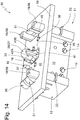
- perspektivische Ansicht von unten des auf der Leiterplatte angeordneten Steckverbinders gemäß
Fig. 1 mit Raststift in Riegelstellung, - Fig. 15:
- Explosionsdarstellung einer zweiten Ausführungsform des Steckverbinders,
- Fig. 16:
- Ansicht des Steckverbinders gemäß
Fig. 15 von oben, - Fig. 17:
- Schnittdarstellung des Steckverbinders gemäß
Fig. 15 entlang der Schnittebene XV-XV gemäßFig. 16 mit Kontaktträger in Vormontagestellung, - Fig. 18:
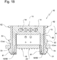
- Schnittdarstellung des Steckverbinders gemäß
Fig. 15 entlang der Schnittebene XVI-XVI gemäßFig. 16 mit Kontaktträger in Montagestellung. - In den Figuren ist ein erfindungsgemäßer Steckverbinder insgesamt mit der Bezugsziffer 10 versehen.
- In den
Figur 1 bis 14 ist eine erste Ausführungsform des Steckverbinders 10 offenbart. Eine zweite Ausführungsform ist in denFiguren 15 bis 18 gezeigt. Baugleiche oder gleichwirkende Bauteile sind mit identischen Bezugszeichen und Begriffen benannt. Soweit nichts Abweichendes aufgeführt ist, gelten die Ausführungen zu einem Ausführungsbeispiel sinngemäß für die alternative Ausführungsform. - In der
Fig. 1 ist neben dem Steckverbinder 10 mit einem Kontaktträger 11 und einer Sekundärsicherung 26, eine Leiterplatte 19 dargestellt. - Der Steckverbinder 10 weist den Kontaktträger 11 auf, welcher ein Gehäuse 13 für Steckkontakte 12 bildet. Das Gehäuse 13 des
- Kontaktträgers 11 ist mit Leitereinschubkanälen 14 versehen, die der Aufnahme von hier nicht dargestellten Anschlussleitern dienen. Diese werden über Schneidklemmgabeln 48 mit den Steckkontakten 12 elektrisch verbunden. Die Steckkontakte 12 bilden die Kontaktfinger 49, welche die Kontaktöffnung 36 einer Leiterplatte 19 untergreifen, sobald der Steckverbinder 10 an der Leiterplatte 19 angeordnet ist, wie beispielsweise in
Fig. 11 dargestellt. - Zudem ist das Gehäuse 13 mit Kontaktausnehmungen 15 ausgestattet, in welche die Steckkontakte 12 eingeschoben werden. Das Gehäuse 13 trägt an seiner Außenfläche mehrere Kodierstifte 16, welche dem Steckverbinder 10 in Steckrichtung vorspringen und den Steckverbinder 10 an der Leiterplatte 19 mit korrespondierender Kodierung, insbesondere in Form von Kodierbohrungen 37, zuordnen.
- Das Gehäuse 13 weist an seiner Frontseite 20 Rasthaken 21 auf, mittels derer mehrere Steckverbinder 10 zu Konfektionierungszwecken aneinander angeordnet werden können. Auf der Rückseite 22 des Kontaktträgers 11 bildet das Gehäuse 13 Konturen zur Aufnahme 23 von Rasthaken 21 aus, mittels derer weitere Steckverbinder 10 an dem Kontaktträger 11 anordenbar sind.
- Weiterhin ist der Kontaktträger 11 mit einer Verpolungssicherung 18 ausgestattet. Die Verpolungssicherung 18 soll eine kurzschlussgefährdende Kontaktierung der Steckkontakte 12 mit den Kontaktöffnungen 36 der Leiterplatte 19 vermeiden. Die Verpolungssicherung 18 wird von drei der Unterseite des Kontaktträgers 11 entspringenden Polungsvorsprüngen 56 gebildet, wie beispielsweise in
Fig. 6 dargestellt. Dabei sind bezüglich der Papierebene rechts zwei der Polungsvorsprünge 56 am Kontaktträger 11 ausgebildet, wohingegen links bezüglich der Papierebene nur ein Polungsvorspung 56 ausgebildet ist. - Das Gehäuse 13 des Kontaktträgers 11 ist steckrichtungsparallel mit einer Bohrung 24 durchsetzt. Diese Bohrung 24 weist eine erste Kerbe 25A und eine zweite Kerbe 25B auf. Die zweite Kerbe 25B ist ein optionales und kein zwingendes Merkmal der Bohrung 24.
- Die Bohrung 24 dient der Aufnahme der Sekundärsicherung 26, insbesondere in Form eines Raststiftes 27. Der Raststift 27 weist einen Kopfbereich 28 und einen stiftartigen Grundkörper 29 auf.
- Die
Fig. 2a zeigt den Raststift 27 in Seitenansicht. Der Außenumfang des stiftartigen Grundkörpers 29 des Raststiftes 27 wird teilumfänglich von Montagerastvorsprüngen 47 und Riegelrastvorsprüngen 33 umgeben. Die Montagerastvorsprünge 47 dient der Vormontage des Raststiftes 27 am Kontaktträger 11. Die Riegelrastvorsprünge 33 untergreifen die Leiterplatte 19 und halten den Steckverbinder 10 an der Leiterplatte 19. - Die Riegelrastvorsprünge 33, welche vergrößert in
Fig. 2b dargestellt sind, sind gewindeabschnittartig ausgebildet und dienen dem Verspannen des Kontaktträgers 11 an der Leiterplatte 19. Gleichzeitig ermöglicht die Gewindesteigung ebenfalls einen Ausgleich von Leiterplattentoleranzen. - Der stiftartige Grundkörper 29 des Raststiftes 27 weist einen Schlitz 41 auf, der von einem ersten Seitenwand 40A und eine zweiten Seitenwand 40B begrenzt ist. Der Schlitz 41 ermöglicht eine durchmesserverkleinernde Rückverlagerung der Seitenwände 40A und 40B, welche die Riegelrastvorsprünge 33 tragen.
- Im Kopfbereich 28 ist die Rippe 31 dargestellt. Diese kooperiert mit der ersten oder der zweiten Kerbe 25A, 25B der Bohrung 24 (siehe
Fig. 1 ,Fig. 5 ). Diese Rippe 31 kooperiert je nach Riegelstellung des Raststifts 27 mit der ersten oder zweiten Kerbe 25A, 25B und hält so den Raststift 27 bzw. dessen Riegelrastvorsprünge 33 in der Riegel- oder Entriegelstellung der Sekundärsicherung 26. - Die Rippe 31 und der Kopfbereich 28 des Raststiftes 27 sind in der
Fig. 3 gezeigt. Der Kopfbereich 28 bildet eine Nut 30A aus, welche der Aufnahme eines hier nicht dargestellten Werkzeuges dient und so den Raststift 27 in Riegel- oder Entriegelstellung verlagert. In die Nut 30A kann beispielsweise ein Schraubendreher eingeführt werden, mittels dessen sich der Raststift 27 in der Bohrung 24 um 90° drehen lässt. - Die
Fig. 4 zeigt die Leiterplatte 19 von oben. Die Leiterplatte 19 bildet die Kontaktöffnungen 36 zur Aufnahme der Steckkontakte 12 des Kontaktträgers 11 aus. Weiterhin weist die Leiterplatte 19 einen in der Mitte der Leiterplatte 19 gebildeten Durchbruch 39 mit einer schlüssellochartigen Kontur auf. Diese Kontur unterteilt sich in einen Halmabschnitt 58 und einen Bartabschnitt 38. Der Halmabschnitt 58 dient der Aufnahme des stiftartigen Grundkörpers 29 des Raststiftes 27. Der Bartabschnitt 38 dient der Aufnahme eines Kodierstiftes 16 des Kontaktträgers 11. Beidseitig benachbart dieses Bartabschnittes 38 sind zwei Kodierbohrungen 37 in der Leiterplatte 19 ausgebildet, welche der Aufnahme der übrigen Kodierstifte 16 des Kontaktträges 11 dienen. - Benachbart des Durchbruchs 39 weist die Leiterplatte 19 ein erstes und ein zweites Langloch 35A, 35B auf. Diese Langlöcher 35A und 35B weisen Abschnitte auf, welche zum einen mit einer Primärsicherung 17 und zum anderen mit den Polungsvorsprünge 56 der Verpolungssicherung 18 kooperieren. Das Langloch 35A kooperiert zum einen mit der Primärsicherung 17 und mit einem Polungsvorsprung 56. Das Langloch 35B kooperiert mit der Primärsicherung 17 und mit zwei Polungsvorsprüngen 56 und ist dementsprechend länger ausgebildet als das Langloch 35A. Eine Fehlpositionierung des Steckverbinders 10 an der Leiterplatte 19 ist somit ausgeschlossen.
- Die Primärsicherung 17 ist beispielsweise in den
Fig. 5 bis 7 dargestellt und dient der Anordnung des Kontaktträger 11 an der Leiterplatte 19. Die Primärsicherung 17 wird von zwei Rastarmpaaren ausgebildet. Jedes Rastarmpaar verfügt über einen ersten Rastarm 44 und einen zweiten Rastarm 45. Die Rastarme 44, 45 entspringen jeweils einer vom freien Ende abgewandten Rastarmwurzel 52, die am Kontaktträger 11 angeordnet ist. Die Rastarme 44, 45 weisen jeweils einen Lösenocken 53 auf, welche der Rückverlagerung der Rastarme 44, 45 in eine Lösestellung dienen, um den Steckverbinder 10 von Leiterplatte 19 zu trennen, wenn hier ein entsprechender Druck ausgeübt wird, wobei die Lösenocken ein optionales und somit kein zwingendes Merkmal der Rastarme 44, 45 sind. - Die Rastarme 44, 45 weisen in an ihrem freien Ende Rastorgane 50 und 51 auf, welche verschiedenartige Rastflächen 54 und 55 aufweisen.
- In der
Fig. 8 ist das erste Rastorgan 50 des zweiten Rastarmes 45 dargestellt. Das erste Rastorgan 50 des zweiten Rastarmes 45 bildet eine Rastfläche 54 aus, welche die Leiterplatte 19 untergreift. Diese Rastfläche 54 ist im Wesentlichen orthogonal zur Steckrichtung des Steckverbinders ausgerichtet, also in etwa parallel zur Unterseite 46 der Leiterplatte 19, wie es beispielsweise in derFig. 11 und13 zu entnehmen ist. Der Steckverbinder 10 ist so gegen eine Zugkraft, die beispielsweise von den nicht dargestellten Anschlussleitern aufgebracht werden kann, gesichert. Die Rastfläche 54 des ersten Rastorganes 50 ermöglicht eine Haltekraft von bis zu 60 Newton. - In der
Fig. 9 ist das zweite Rastorgan 51 des Rastarmes 44 dargestellt. Das zweite Rastorgan 51 des Rastarmes 44 weist eine Rastfläche 55 auf, welche ausgehend vom ersten Rastarm 44 in Steckrichtung abfallend ausgebildet ist. - Die Rastfläche 55 dient dem Toleranzausgleich zwischen dem Kontaktträger 11 und der Leiterplatte 19. Die an der Leiterplatte 19 angeordneten Rastarme 44 sind beispielsweise in den
Fig. 11 und13 dargestellt. Leiterplatten 19 mit Minimumstärke untergreift die abfallende Rastfläche 55 vollständig, so dass der nahe dem ersten Rastarm 44 gelegen Flächenursprung dem Steckverbinder 10 ergänzend zur Rastfläche 54 Halt an der Leiterplatte 19 bietet. Leiterplatten 19 mit einer Maximalstärke untergreift die abfallende Rastfläche 55 lediglich mit ihrem dem Ursprung abgewandten Ende, welches dem Steckverbinder 10 ergänzend zur Rastfläche 54 Halt bietet. Je nach Zwischenstärke von der Leiterplatte 19 findet ein Teiluntergreifen der Rastfläche 55 statt. - In einer besonders bevorzugten Ausführung schließt die abfallende Rastfläche 55 mit der Unterseite 46 der Leiterplatte 19 einen Winkel von 20° ein und ermöglicht so ein Toleranzausgleich von bis zu 10% der Nennstärke der Leiterplatte 19. Auch die abfallende Rastfläche 55 trägt zur Verankerung des Steckverbinders 10 an der Leiterplatte 19 bei. Die durch sie kompensierbare Zugbelastung ist aufgrund der abfallend gerichteten Rastfläche 55 jedoch gering.
- Die Rastarme 44, 45 eilen dem Kontaktträger 11 vor und sind zueinander parallel angeordnet. Der Steckverbinder 10 verfügt über zwei Rastarmpaaren, die an gegenüberliegenden Seiten des Steckverbinders 10 angeordnet sind. Die Rastorgane 50 und 51 gleicher Rastgeometrie liegen einander diagonal am Kontaktträger 11 gegenüber. Am Beispiel der
Fig.11 lässt sich erkennen, dass das Rastorgan 51 des bezüglich der Papierebene linken Rastarmpaares vorne, das Rastorgan 50 hingegen hinten angeordnet ist. Das bezüglich der Papierebene rechte Rastarmpaar verfügt hingegen über ein vorn liegendes Rastorgan 50, wohingegen das Rastorgan 51 hinten gelegen ist. Auf diese Weise wird die vorerwähnte Diagonalität gewährleistet. - Durch die diagonal gegenüberliegenden Rastorgane 50 und 51 gleicher Ausgestaltung mit ihren Rastflächen 54 und 55 wird das Verkippen des Steckverbinders 19 unter Zugbelastung verhindert und somit die Kontaktstellenbelastung zwischen den Steckkontakten 12 und den Kontaktlöchern 36 vergleichmäßigt.
- In den
Figuren 10 und11 ist die Sekundärsicherung 26 in Entriegelstellung gelagert und in Ansicht von oben (Fig. 10 ) und von unten (Fig. 11 ) dargestellt. Die Entriegelstellung wird hier angezeigt, indem die Nut 30A auf das Wort "release" zeigt. Eine andere Form der optischen Anzeige ist möglich. In der Entriegelstellung kooperiert die Rippe 31 des Kopfbereiches 28 des Raststiftes 27 mit der ersten, dem Begriff "release" zugeordneten Kerbe 25A. In dieser Stellung halten die Rippe 31 und die erste Kerbe 25A den Raststiftes 27 in der Entriegelstellung. Ein selbstständiges Drehen des Raststiftes 27 bzw. durch Erschütterung ist nicht möglich. Die Sekundärsicherung 26 ist lediglich so in dem Halmabschnitt 58 des Durchbruches 39 gelagert, dass die Riegelrastvorsprünge 33 des Raststiftes 27 die Leiterplatte 19 nicht untergreifen. - In den
Figuren 12 bis 14 ist der Raststift 27 in Riegelstellung verlagert. Der drehbar gelagerte Raststift 27 ermöglicht es den Kontaktträger 11 mit der Leiterplatte 19 zu verspannen, indem der Raststift 27 bei auf der Leiterplatte 19 montiertem Steckverbinder 10 von der Entriegelstellung in die Riegelstellung verdreht wird. Der Raststift 27 ist in Riegelstellung so im Halmbereich 58 des Durchbruches 39 gelagert, dass die Riegelrastvorsprünge 33 des Riegelstiftes 27 die Leiterplatte 19 untergreifen und durch die gewindeabschnittartige Ausgestaltung der Riegelrastvorsprünge 33 den Kontaktträger 11 mit der Leiterplatte 19 verspannen. - Alternativ kann sich der Raststift 27 beim Aufsetzen auf der Leiterplatte 19 bereits in Riegelstellung befinden. Dann laufen die Riegelrastvorsprünge 33 auf den Rand des Durchbruchs 39 auf. Der vertikal im Raststift 27 angeordnete Schlitz 41 ermöglicht beim Fortführen des Raststifts eine rückstellelastische Rückverlagerung der Riegelrastvorsprünge 33 des Raststifts 27, so dass diese durch den Durchbruch 39 hindurch tauschen und so die Leiterplatte 19 untergreifen.
- In der Riegelstellung des Raststiftes 27, kooperiert die Rippe 31 des Kopfbereiches 28 des Raststiftes 27 nun mit der zweiten Kerbe 25B der Bohrung 24. Die Riegelstellung ist mit dem Wort "lock" gekennzeichnet. Die Nut 30A weist auf das Wort "lock". Der Steckverbinder 10 ist an der Leiterplatte 19 sicher montiert.
- In den
Figuren 15 bis 18 ist eine zweite Ausführungsform des Steckverbinders 10 offenbart. Zusätzlich zu den benannten Bauteilen des Steckverbinders 10 der ersten Ausführungsform, weist dieser Steckverbinder 10 eine Sicherungshaube 60 auf. - In der
Fig. 15 ist neben dem Steckverbinder 10 mit Kontaktträger 11 und Sicherungshaube 60, die Leiterplatte 19 dargestellt. - Die Sicherungshaube 60 umgibt den Kontaktträger 11 außenumfänglich, wobei der Kontaktträger 11 in der Sicherungshaube 60 beweglich angeordnet ist. Der Kontaktträger 11 weist steckrichtungsparallel Riegelzapfen 61 auf, welche dem Kontaktträger 11 voreilen und diesen in der Sicherungshaube 60 in Vormontagestellung positionieren.
- Zudem bildet der Kontaktträger 11 Rastprofile 63 und Rastnuten 66 aus, welche dem Kontaktträger 11 in Steckrichtung voreilen und entsprechend der Vor- oder Montagestellung des Kontaktträgers 11 in der Sicherungshaube 60 mit Raststegen 65 der Sicherungshaube 60 kooperieren.
- Weiterhin weist der Kontaktträger 11 Rastlaschen 62 auf, welche dem Gehäuse 13 an den jeweils kurzen Seiten des Kontaktträgers 11 entspringen. Die Rastlaschen 62 sind rückstellelastisch ausgebildet und kooperieren mit Rastöffnungen 64, welche von der Sicherungshaube 60 ausgebildet werden, wie es in
Fig. 16 dargestellt ist. Durch die Kooperation von Rastlaschen 62 und Rastöffnungen 64 wird der Kontaktträger 11 an der Sicherungshaube 60 verrastet. Durch Druck können die Rastlaschen 62 rückverlagert werden, so dass der Kontaktträger 11 von der Sicherungshaube 60 gelöst werden kann. - Zudem bildet die Rastlasche 62 eine Rastnase 67 aus, die mit einer korrespondieren Rastausnehmung 68, welche von der Sicherungshaube 60 ausgebildet wird, kooperiert. Sobald der Kontaktträger 11 in Montagestellung bewegt wird, wirkt die Rastnase 67 mit der Rastausnehmung 68 zusammen, wie in der Schnittdarstellung in
Fig. 17 dargestellt. Die Rastnase 67 taucht durch die Rastausnehmung 68 hindurch und befestigt so den Kontaktträger 11 zusätzlich in der Sicherungshaube 60. Durch die Rückverlagerung der Rastlaschen 62 werden auch die Rastnasen rückverlagert, sodass der Kontaktträger 11 von der Sicherungshaube gelöst werden kann. - Im Gegensatz zu der ersten Ausführungform des Steckverbinders 10, entspringen die Primärsicherung 17, die Verpolungssicherung 18 und die Kodierstifte 16 der Sicherungshaube 60 nicht dem Kontaktträger 11. Die Primärsicherung 17 weist in dieser zweiten Ausführungsform des Steckverbinders 10 beidseitig identische Rastarmpaare 44 auf, welche mit den Rastorganen 51 ausgebildet sind. Die Rastorgane weisen die Rastfläche 55 auf, welche dem Toleranzausgleich zwischen Kontaktträger 11 und der Leiterplatte 19 dienen.
- Es ist allerdings auch denkbar, dass die Primärsicherung 17 identisch der ersten Ausführungsform des Steckverbinders 10 ausgestaltet ist, wie beispielsweise in
Fig. 5 dargestellt. - Auch die Verpolungssicherung 18 kann entsprechend der ersten Ausführungsform des Steckverbinders 10 ausgestaltet sein, wie es exemplarisch der
Fig. 6 zu entnehmen ist. - Zur Konfektionierung des Steckverbinders 10 an der Leiterplatte 19 müssen die Kontaktfinger 49 der Steckkontakte 12 in die Kontaktöffnungen 36 der Leiterplatte 19 aufgenommen werden, um eine elektrische Kontaktierung herzustellen.
- Der Kontaktträger 11 wird mittels Riegelzapfen 61 in der Sicherungshaube 60 positioniert, wobei die Rastnuten 66 des Kontaktträger 11 in Vormontagestellung mit den Raststegen 65 des Sicherungshaube 60 kooperieren. Die Steckkontakte 12 sind in den Kontaktausnehmungen 15 des Kontaktträgers 11 eingeschoben. Da der Kontaktträger 11 und dementsprechend auch die Steckkontakte 12 in der Vormontagestellung beabstandet von der Leiterplatte 19 vorliegen, ist eine elektrische Kontaktierung des Steckverbinders 10 mit der Leiterplatte 19 in der Vormontagestellung des Steckverbinders 10 ausgeschlossen.
- Um den Steckverbinder 10 fertig zu konfektionieren, wird der Kontaktträger 11 in Steckrichtung bewegt und somit in Montagestellung verlagert. Die Raststege 66 greifen nun in die Rastprofile 63 des Kontaktträgers 11 ein und ordnen so den Kontaktträger 11 in der Sichererungshaube 60 an. Zusätzlich rasten die Rastlaschen 62 an den Rastöffnungen 64 der Sicherungshaube 60 fest. Mit der Verlagerung des Kontaktträgerträgers 11 in Steckrichtung werden neben den Kodierstiften 16, welche die Kodierbohrungen 37 der Leiterplatte 19 durchdringen, auch die Steckkontakte 12 in Steckrichtung verlagert. Dadurch kooperieren die Kontaktfinger 49 der Steckkontakte 12 mit den Kontaktöffnungen 36 in der Leiterplatte 19 und ermöglichen so die elektrische Kontaktierung.
- Die
Fig. 17 zeigt den in Vormontagestellung befindlichen Steckverbinder 10 an der Leiterplatte 19. - In der
Fig. 17 ist die Sicherungshaube 60 der Leiterplatte 19 angeordnet. Die Rastflächen 55 der Rastarme 44 untergreifen die Leiterplatte 19 und legen die Sicherungshaube 60 an der Leiterplatte 19 fest. - Der Kontaktträger 11 ist in Vormontagestellung in der Sicherungshaube 60 angeordnet. Die Riegelzapfen 61 des Kontaktträgers 11 sitzen in einem oberen Bereich A oberhalb der Rastarme 44. Somit ist der für eine lösende Rückverlagerung der Rastarme erforderliche Bewegungsraum frei. Die Rastarme 44 können mittels Druck auf die Lösenocken 53 in den Bewegungsraum rückverlagert werden und so die Sicherungshaube 60 leicht von der Leiterplatte 19 gelöst werden.
- Wird der Kontaktträger 11, wie in
Fig. 18 dargestellt, in der Sicherungshaube 60 in Montagestellung verlagert, werden die Riegelzapfen 61 in Steckrichtung bewegt und dringen in den vorerwähnten Bewegungsraum ein und blockieren so die lösende Rückverlagerung der Rastarme 44. Aufgrund der Blockierung ist es nunmehr unmöglich, den Steckverbinder 10 von der Leiterplatte 19 zu lösen. Eine sichere und dauerhafte Kontaktierung ist dadurch gewährleistet. -
- 10
- Steckverbinder
- 11
- Kontaktträger
- 12
- Steckkontakt
- 13
- Gehäuse
- 14
- Leitereinschubkanal
- 15
- Kontaktausnehmung
- 16
- Kodierstift
- 17
- Primärsicherung
- 18
- Verpolungssicherung
- 19
- Leiterplatte
- 20
- Frontseite
- 21
- Rasthaken
- 22
- Rückseite
- 23
- Konturen zur Aufnahme von 21
- 24
- Bohrung
- 25A
- erste Kerbe
- 25B
- zweite Kerbe
- 26
- Sekundärsicherung
- 27
- Raststift
- 28
- Kopfbereich
- 29
- Grundkörper
- 30
- Werkzeugansatz
- 30A
- Nut
- 31
- Rippe
- 33
- Riegelrastvorsprünge
- 35A
- erstes Langloch
- 35B
- zweites Langloch
- 36
- Kontaktöffnungen
- 37
- Kodierbohrung
- 38
- Bartabschnitt
- 39
- Durchbruch
- 40A
- erste Seitenwand von 29
- 40B
- zweite Seitenwand von 29
- 41
- Schlitz
- 42A
- Seite A von 24
- 42B
- Seite B von 24
- 44
- erster Rastarm
- 45
- zweiter Rastarm
- 46
- Unterseite von 19
- 47
- Montagerastvorsprünge
- 48
- Schneidklemmgabel
- 49
- Kontaktfinger
- 50
- erstes Rastorgan
- 51
- zweites Rastorgan
- 52
- Rastarmwurzel
- 53
- Lösenocken
- 54
- erste Rastfläche
- 55
- zweite Rastfläche
- 56
- Polungsvorsprung
- 58
- Halmabschnitt
- 60
- Sicherungshaube
- 61
- Riegelzapfen
- 62
- Rasttasche
- 63
- Rastprofil
- 64
- Rastöffnung
- 65
- Raststeg
- 66
- Rastnuten
- 67
- Rastnase
- 68
- Rastausnehmung
- A
- oberer Bereich der Rastarme 44
- IIb
- Ausschnittskreis
Claims (10)
- Steckverbinder (10), insbesondere Direktsteckverbinder zur Kontaktierung von Kontaktöffnungen (36) einer Leiterplatte (19),- mit einem Kontaktträger (11), welcher über Kodiermittel, insbesondere Kodierstifte (16) und eine Verpolungssicherung (18), insbesondere in Form von Polungsvorsprüngen (56) verfügen kann,- mit vom Kontaktträger (11) ausgebildeten Leitereinschubkanälen (14) zur Aufnahme von Anschlussleitern sowie mit Kontaktausnehmungen (15) zur Aufnahme von Steckkontakten (12),- mit einer Sicherungshaube (60), welche den Kontaktträger (11) umgibt, wobei der Kontaktträger (11) in der Sicherungshaube (60) in Steckrichtung des Steckverbinders 810) verschieblich zwischen einer Montagestellung und einer Vormontagestellung verlagerbar ist,- mit einer den Steckverbinder (10) an der Leiterplatte (19) haltenden Primärsicherung (17), welche Teil der Sicherungshaube (60) ist, wobei die Primärsicherung (17) von einer Riegelstellung in eine Lösestellung verlagerbar ist,dadurch gekennzeichnet, dass der Kontaktträger (11) in seiner Montagestellung innerhalb der Sicherungshaube (60) die Primärsicherung (17) in ihrer Riegelstellung hält.
- Steckverbinder (10) nach Anspruch 1, dadurch gekennzeichnet, dass die Primärsicherung (17) zumindest einen an der Sicherungshaube (60) angeordneten Rastarm (44, 45) umfasst, welcher sich in Steckrichtung erstreckt.
- Steckverbinder (10) nach Anspruch 2, dadurch gekennzeichnet, dass der Kontaktträger (11) in seiner Montagestellung in demjenigen Raum angeordnet ist, in welchen der Rastarm (44, 45) zur Einnahme der Lösestellung zu verlagern ist und so die Verlagerungsbewegung des Rastarmes (44, 45) in die Lösestellung blockiert.
- Steckverbinder (10) nach Anspruch 3, dadurch gekennzeichnet, dass die Primärsicherung (17) wenigstens zwei einander gegenüberliegende Rastarme (44, 45) aufweist, wobei der Raum zur Anordnung des Kontaktträger (11) in seiner Montagestellung zwischen den Rastarmen (44, 45) aufgespannt ist.
- Steckverbinder (10) nach Anspruch 2, dadurch gekennzeichnet, dass die Primärsicherung (17) wenigstens zwei paarweise nebeneinander angeordnete Rastarme (44, 45) umfasst, deren Rastorgane (50, 51) unterschiedliche Rastgeometrien aufweisen.
- Steckverbinder (10) nach Anspruch 5, dadurch gekennzeichnet, dass das Rastorgan (50) des ersten Rastarms (45) eine die Leiterplatte untergreifende Rastfläche (54) aufweist, welche im Wesentlichen orthogonal zur Steckrichtung des Steckverbinders (10) ausgerichtet ist.
- Steckverbinder (10) nach den Ansprüchen 5 und 6, dadurch gekennzeichnet, dass das Rastorgan (51) des zweiten Rastarmes (44) eine die Leiterplatte (19) zumindest teiluntergreifende Rastfläche (55) aufweist, welche ausgehend vom Rastarm (44) in Steckrichtung abfallend ausgebildet ist.
- Steckverbinder (10) nach einem der vorhergehenden Ansprüche, dadurch gekennzeichnet, dass die Sicherungshaube (60) zwei einander gegenüberliegend angeordnete und in Steckrichtung orientierte Rastarmpaare aufweist.
- Steckverbinder (10) nach Anspruch 8, dadurch gekennzeichnet, dass Rastarme (44, 45) unterschiedlicher Rastarmpaare mit Rastorganen (50, 51) gleicher Geometrie einander diagonal gegenüberliegen.
- Steckverbinder (10) nach einem der vorhergehenden Ansprüche, dadurch gekennzeichnet, dass jeder Rastarme (44, 45) einen Lösenocken (53) aufweist, der der Rückverlagerung des Rastorgans (50, 51) in den Raum der Lösestellung dient, um den Steckverbinder (10) von der Leiterplatte (19) zu trennen, wobei der Kontaktträger (11) in Vormontagestellung verlagert ist.
Priority Applications (1)
| Application Number | Priority Date | Filing Date | Title |
|---|---|---|---|
| SI201830061T SI3518347T1 (sl) | 2018-01-25 | 2018-10-16 | Konektor z zapahnilnim zaščitnim plaščem |
Applications Claiming Priority (1)
| Application Number | Priority Date | Filing Date | Title |
|---|---|---|---|
| DE102018101669.7A DE102018101669B3 (de) | 2018-01-25 | 2018-01-25 | Steckverbinder mit verriegelnder Sicherungshaube |
Publications (2)
| Publication Number | Publication Date |
|---|---|
| EP3518347A1 true EP3518347A1 (de) | 2019-07-31 |
| EP3518347B1 EP3518347B1 (de) | 2020-02-26 |
Family
ID=63878366
Family Applications (1)
| Application Number | Title | Priority Date | Filing Date |
|---|---|---|---|
| EP18200624.7A Active EP3518347B1 (de) | 2018-01-25 | 2018-10-16 | Steckverbinder mit verriegelnder sicherungshaube |
Country Status (4)
| Country | Link |
|---|---|
| EP (1) | EP3518347B1 (de) |
| DE (1) | DE102018101669B3 (de) |
| ES (1) | ES2784006T3 (de) |
| SI (1) | SI3518347T1 (de) |
Cited By (4)
| Publication number | Priority date | Publication date | Assignee | Title |
|---|---|---|---|---|
| LU101642B1 (de) * | 2020-02-13 | 2021-08-13 | Phoenix Contact Gmbh & Co | Steckverbinder, Steckkontaktträger, Gehäuse und Verfahren zur Herstellung eines Steckverbinders |
| LU101643B1 (de) * | 2020-02-13 | 2021-08-13 | Phoenix Contact Gmbh & Co | Steckkontaktelement, Direktsteckverbinder, Verfahren zur Herstellung eines Steckkontaktelementes und Verfahren zur Herstellung eines Direktsteckverbinders |
| CN115053411A (zh) * | 2020-02-13 | 2022-09-13 | 菲尼克斯电气公司 | 由插接接触载体和至少一个插接接触元件构成的系统、插接接触载体、插接接触元件和插接连接器 |
| CN115995702A (zh) * | 2021-10-19 | 2023-04-21 | 迈恩德电子有限公司 | 用于电路板的电路板插头 |
Families Citing this family (1)
| Publication number | Priority date | Publication date | Assignee | Title |
|---|---|---|---|---|
| DE202021101264U1 (de) * | 2021-03-12 | 2022-07-19 | WAGO Verwaltungsgesellschaft mit beschränkter Haftung | Rastfuß und Set aus einer Leiteranschlussklemme und einem Rastfuß |
Citations (4)
| Publication number | Priority date | Publication date | Assignee | Title |
|---|---|---|---|---|
| EP0020834A1 (de) * | 1979-06-28 | 1981-01-07 | AMP INCORPORATED (a New Jersey corporation) | Elektrische Steckereinheit und Verriegelungsglied für solch eine Einheit |
| US20120129373A1 (en) * | 2010-11-18 | 2012-05-24 | Tyco Electronics Corporation | Electrical connector assembly having connector shroud |
| US20160211595A1 (en) * | 2015-01-21 | 2016-07-21 | Hong Fu Jin Precision Industry (Wuhan) Co., Ltd. | Connector and connector assembly |
| DE202016105525U1 (de) * | 2016-10-05 | 2018-01-08 | Lumberg Connect Gmbh | Steckverbinder mit entfernbaren Kodierstiften |
Family Cites Families (2)
| Publication number | Priority date | Publication date | Assignee | Title |
|---|---|---|---|---|
| DE102011011017A1 (de) | 2011-02-11 | 2012-08-16 | Würth Elektronik Ics Gmbh & Co. Kg | Direktsteckvorrichtung mit Stecker und Schürze |
| DE102013218441A1 (de) | 2013-09-13 | 2015-04-02 | Würth Elektronik Ics Gmbh & Co. Kg | Direktsteckvorrichtung mit Vorjustiereinrichtung und relativ zu dieser verschiebbarer Verriegelungseinrichtung |
-
2018
- 2018-01-25 DE DE102018101669.7A patent/DE102018101669B3/de active Active
- 2018-10-16 ES ES18200624T patent/ES2784006T3/es active Active
- 2018-10-16 SI SI201830061T patent/SI3518347T1/sl unknown
- 2018-10-16 EP EP18200624.7A patent/EP3518347B1/de active Active
Patent Citations (4)
| Publication number | Priority date | Publication date | Assignee | Title |
|---|---|---|---|---|
| EP0020834A1 (de) * | 1979-06-28 | 1981-01-07 | AMP INCORPORATED (a New Jersey corporation) | Elektrische Steckereinheit und Verriegelungsglied für solch eine Einheit |
| US20120129373A1 (en) * | 2010-11-18 | 2012-05-24 | Tyco Electronics Corporation | Electrical connector assembly having connector shroud |
| US20160211595A1 (en) * | 2015-01-21 | 2016-07-21 | Hong Fu Jin Precision Industry (Wuhan) Co., Ltd. | Connector and connector assembly |
| DE202016105525U1 (de) * | 2016-10-05 | 2018-01-08 | Lumberg Connect Gmbh | Steckverbinder mit entfernbaren Kodierstiften |
Cited By (8)
| Publication number | Priority date | Publication date | Assignee | Title |
|---|---|---|---|---|
| LU101642B1 (de) * | 2020-02-13 | 2021-08-13 | Phoenix Contact Gmbh & Co | Steckverbinder, Steckkontaktträger, Gehäuse und Verfahren zur Herstellung eines Steckverbinders |
| LU101643B1 (de) * | 2020-02-13 | 2021-08-13 | Phoenix Contact Gmbh & Co | Steckkontaktelement, Direktsteckverbinder, Verfahren zur Herstellung eines Steckkontaktelementes und Verfahren zur Herstellung eines Direktsteckverbinders |
| WO2021160427A1 (de) * | 2020-02-13 | 2021-08-19 | Phoenix Contact Gmbh & Co. Kg | Steckkontaktelement, direktsteckverbinder, verfahren zur herstellung eines steckkontaktelementes und verfahren zur herstellung eines direktsteckverbinders |
| WO2021160428A1 (de) * | 2020-02-13 | 2021-08-19 | Phoenix Contact Gmbh & Co. Kg | Steckverbinder, steckkontaktträger, gehäuse und verfahren zur herstellung eines steckverbinders |
| CN115039292A (zh) * | 2020-02-13 | 2022-09-09 | 菲尼克斯电气公司 | 插接连接器、插接接触载体、壳体和用于制造插接连接器的方法 |
| CN115053411A (zh) * | 2020-02-13 | 2022-09-13 | 菲尼克斯电气公司 | 由插接接触载体和至少一个插接接触元件构成的系统、插接接触载体、插接接触元件和插接连接器 |
| CN115053407A (zh) * | 2020-02-13 | 2022-09-13 | 菲尼克斯电气公司 | 插塞接触元件,直接插塞连接器,用于制造插塞接触元件的方法和用于制造直接插塞连接器的方法 |
| CN115995702A (zh) * | 2021-10-19 | 2023-04-21 | 迈恩德电子有限公司 | 用于电路板的电路板插头 |
Also Published As
| Publication number | Publication date |
|---|---|
| SI3518347T1 (sl) | 2020-07-31 |
| DE102018101669B3 (de) | 2019-03-28 |
| ES2784006T3 (es) | 2020-09-21 |
| EP3518347B1 (de) | 2020-02-26 |
Similar Documents
| Publication | Publication Date | Title |
|---|---|---|
| EP3518345B1 (de) | Steckverbinder mit sekundärsicherung | |
| EP3518347B1 (de) | Steckverbinder mit verriegelnder sicherungshaube | |
| DE102007023882B4 (de) | Elektrischer Verbinder | |
| DE19813458B4 (de) | Elektrischer Verbinder | |
| DE102013110082C5 (de) | Steckverbinder | |
| DE102018113365A1 (de) | Modulares Steckverbindersystem | |
| EP3518346B1 (de) | Steckverbinder mit primärverriegelnden rastarmen | |
| WO2019233763A1 (de) | Sicherungssystem für steckverbinder | |
| DE102015201089A1 (de) | Zwischengehäuse mit einer CPA-Aufnahme und Steckverbindersysteme umfassend ein solches | |
| EP3852201A1 (de) | Direktstecksystem für die verbindung eines steckverbinders mit einer leiterplatte | |
| DE102018215088A1 (de) | Verbinder | |
| EP3257121A1 (de) | ANORDNUNG MEHRERER RASTFÜßE FÜR EINE BAUGRUPPE UND BAUGRUPPE | |
| DE202018100416U1 (de) | Steckverbinder mit verriegelnder Sicherungshaube | |
| EP0865105B1 (de) | Steckbuchse bzw. elektrischer Steckverbinder mit Kontaktfeder und Steckbuchse als Anschlusskontakt | |
| EP3698440B1 (de) | Befestigungsklemme | |
| EP3066723B1 (de) | Prüfkabel sowie buchsenadapter für ein prüfkabel | |
| EP3793036B1 (de) | Kontaktbuchse, leiterplattenanordnung und stecksystem damit | |
| EP3306755B1 (de) | Direktsteckverbinder mit entfernbaren kodierstiften | |
| EP3621157A1 (de) | Elektrische steckbuchse | |
| DE202018100413U1 (de) | Steckverbinder mit Sekundärsicherung | |
| EP3886267A1 (de) | Steckverbinderbaugruppe, stecksystem und verfahren | |
| DE102006013281A1 (de) | Steckverbindungs-Adapter | |
| DE202018100417U1 (de) | Steckverbinder mit primärverriegelnden Rastarmen | |
| DE102016118147A1 (de) | Steckkontakt mit Schneid-Klemm-Gabel | |
| DE102012221986B4 (de) | Kontaktgehäuse für ein elektrisches Steckerelement sowie selbiges und Bausatz für ein elektrisches Steckerelement |
Legal Events
| Date | Code | Title | Description |
|---|---|---|---|
| PUAI | Public reference made under article 153(3) epc to a published international application that has entered the european phase |
Free format text: ORIGINAL CODE: 0009012 |
|
| STAA | Information on the status of an ep patent application or granted ep patent |
Free format text: STATUS: REQUEST FOR EXAMINATION WAS MADE |
|
| 17P | Request for examination filed |
Effective date: 20190611 |
|
| AK | Designated contracting states |
Kind code of ref document: A1 Designated state(s): AL AT BE BG CH CY CZ DE DK EE ES FI FR GB GR HR HU IE IS IT LI LT LU LV MC MK MT NL NO PL PT RO RS SE SI SK SM TR |
|
| AX | Request for extension of the european patent |
Extension state: BA ME |
|
| STAA | Information on the status of an ep patent application or granted ep patent |
Free format text: STATUS: EXAMINATION IS IN PROGRESS |
|
| 17Q | First examination report despatched |
Effective date: 20190828 |
|
| RIC1 | Information provided on ipc code assigned before grant |
Ipc: H01R 12/71 20110101AFI20191016BHEP Ipc: H01R 12/70 20110101ALN20191016BHEP Ipc: H01R 13/645 20060101ALN20191016BHEP Ipc: H01R 12/51 20110101ALI20191016BHEP Ipc: H01R 13/516 20060101ALI20191016BHEP |
|
| RIC1 | Information provided on ipc code assigned before grant |
Ipc: H01R 13/516 20060101ALI20191018BHEP Ipc: H01R 12/51 20110101ALI20191018BHEP Ipc: H01R 12/71 20110101AFI20191018BHEP Ipc: H01R 12/70 20110101ALN20191018BHEP Ipc: H01R 13/645 20060101ALN20191018BHEP |
|
| GRAP | Despatch of communication of intention to grant a patent |
Free format text: ORIGINAL CODE: EPIDOSNIGR1 |
|
| STAA | Information on the status of an ep patent application or granted ep patent |
Free format text: STATUS: GRANT OF PATENT IS INTENDED |
|
| RIC1 | Information provided on ipc code assigned before grant |
Ipc: H01R 12/71 20110101AFI20191119BHEP Ipc: H01R 12/70 20110101ALN20191119BHEP Ipc: H01R 13/516 20060101ALI20191119BHEP Ipc: H01R 13/645 20060101ALN20191119BHEP Ipc: H01R 12/51 20110101ALI20191119BHEP |
|
| INTG | Intention to grant announced |
Effective date: 20191203 |
|
| GRAS | Grant fee paid |
Free format text: ORIGINAL CODE: EPIDOSNIGR3 |
|
| GRAA | (expected) grant |
Free format text: ORIGINAL CODE: 0009210 |
|
| STAA | Information on the status of an ep patent application or granted ep patent |
Free format text: STATUS: THE PATENT HAS BEEN GRANTED |
|
| AK | Designated contracting states |
Kind code of ref document: B1 Designated state(s): AL AT BE BG CH CY CZ DE DK EE ES FI FR GB GR HR HU IE IS IT LI LT LU LV MC MK MT NL NO PL PT RO RS SE SI SK SM TR |
|
| REG | Reference to a national code |
Ref country code: GB Ref legal event code: FG4D Free format text: NOT ENGLISH |
|
| REG | Reference to a national code |
Ref country code: CH Ref legal event code: EP |
|
| REG | Reference to a national code |
Ref country code: DE Ref legal event code: R096 Ref document number: 502018000838 Country of ref document: DE |
|
| REG | Reference to a national code |
Ref country code: AT Ref legal event code: REF Ref document number: 1238786 Country of ref document: AT Kind code of ref document: T Effective date: 20200315 |
|
| REG | Reference to a national code |
Ref country code: IE Ref legal event code: FG4D Free format text: LANGUAGE OF EP DOCUMENT: GERMAN |
|
| PG25 | Lapsed in a contracting state [announced via postgrant information from national office to epo] |
Ref country code: FI Free format text: LAPSE BECAUSE OF FAILURE TO SUBMIT A TRANSLATION OF THE DESCRIPTION OR TO PAY THE FEE WITHIN THE PRESCRIBED TIME-LIMIT Effective date: 20200226 Ref country code: NO Free format text: LAPSE BECAUSE OF FAILURE TO SUBMIT A TRANSLATION OF THE DESCRIPTION OR TO PAY THE FEE WITHIN THE PRESCRIBED TIME-LIMIT Effective date: 20200526 Ref country code: RS Free format text: LAPSE BECAUSE OF FAILURE TO SUBMIT A TRANSLATION OF THE DESCRIPTION OR TO PAY THE FEE WITHIN THE PRESCRIBED TIME-LIMIT Effective date: 20200226 |
|
| REG | Reference to a national code |
Ref country code: NL Ref legal event code: MP Effective date: 20200226 |
|
| REG | Reference to a national code |
Ref country code: LT Ref legal event code: MG4D |
|
| PG25 | Lapsed in a contracting state [announced via postgrant information from national office to epo] |
Ref country code: LV Free format text: LAPSE BECAUSE OF FAILURE TO SUBMIT A TRANSLATION OF THE DESCRIPTION OR TO PAY THE FEE WITHIN THE PRESCRIBED TIME-LIMIT Effective date: 20200226 Ref country code: IS Free format text: LAPSE BECAUSE OF FAILURE TO SUBMIT A TRANSLATION OF THE DESCRIPTION OR TO PAY THE FEE WITHIN THE PRESCRIBED TIME-LIMIT Effective date: 20200626 Ref country code: HR Free format text: LAPSE BECAUSE OF FAILURE TO SUBMIT A TRANSLATION OF THE DESCRIPTION OR TO PAY THE FEE WITHIN THE PRESCRIBED TIME-LIMIT Effective date: 20200226 Ref country code: GR Free format text: LAPSE BECAUSE OF FAILURE TO SUBMIT A TRANSLATION OF THE DESCRIPTION OR TO PAY THE FEE WITHIN THE PRESCRIBED TIME-LIMIT Effective date: 20200527 Ref country code: SE Free format text: LAPSE BECAUSE OF FAILURE TO SUBMIT A TRANSLATION OF THE DESCRIPTION OR TO PAY THE FEE WITHIN THE PRESCRIBED TIME-LIMIT Effective date: 20200226 Ref country code: BG Free format text: LAPSE BECAUSE OF FAILURE TO SUBMIT A TRANSLATION OF THE DESCRIPTION OR TO PAY THE FEE WITHIN THE PRESCRIBED TIME-LIMIT Effective date: 20200526 |
|
| REG | Reference to a national code |
Ref country code: ES Ref legal event code: FG2A Ref document number: 2784006 Country of ref document: ES Kind code of ref document: T3 Effective date: 20200921 |
|
| PG25 | Lapsed in a contracting state [announced via postgrant information from national office to epo] |
Ref country code: NL Free format text: LAPSE BECAUSE OF FAILURE TO SUBMIT A TRANSLATION OF THE DESCRIPTION OR TO PAY THE FEE WITHIN THE PRESCRIBED TIME-LIMIT Effective date: 20200226 |
|
| PG25 | Lapsed in a contracting state [announced via postgrant information from national office to epo] |
Ref country code: SM Free format text: LAPSE BECAUSE OF FAILURE TO SUBMIT A TRANSLATION OF THE DESCRIPTION OR TO PAY THE FEE WITHIN THE PRESCRIBED TIME-LIMIT Effective date: 20200226 Ref country code: EE Free format text: LAPSE BECAUSE OF FAILURE TO SUBMIT A TRANSLATION OF THE DESCRIPTION OR TO PAY THE FEE WITHIN THE PRESCRIBED TIME-LIMIT Effective date: 20200226 Ref country code: LT Free format text: LAPSE BECAUSE OF FAILURE TO SUBMIT A TRANSLATION OF THE DESCRIPTION OR TO PAY THE FEE WITHIN THE PRESCRIBED TIME-LIMIT Effective date: 20200226 Ref country code: DK Free format text: LAPSE BECAUSE OF FAILURE TO SUBMIT A TRANSLATION OF THE DESCRIPTION OR TO PAY THE FEE WITHIN THE PRESCRIBED TIME-LIMIT Effective date: 20200226 Ref country code: PT Free format text: LAPSE BECAUSE OF FAILURE TO SUBMIT A TRANSLATION OF THE DESCRIPTION OR TO PAY THE FEE WITHIN THE PRESCRIBED TIME-LIMIT Effective date: 20200719 Ref country code: CZ Free format text: LAPSE BECAUSE OF FAILURE TO SUBMIT A TRANSLATION OF THE DESCRIPTION OR TO PAY THE FEE WITHIN THE PRESCRIBED TIME-LIMIT Effective date: 20200226 Ref country code: RO Free format text: LAPSE BECAUSE OF FAILURE TO SUBMIT A TRANSLATION OF THE DESCRIPTION OR TO PAY THE FEE WITHIN THE PRESCRIBED TIME-LIMIT Effective date: 20200226 Ref country code: SK Free format text: LAPSE BECAUSE OF FAILURE TO SUBMIT A TRANSLATION OF THE DESCRIPTION OR TO PAY THE FEE WITHIN THE PRESCRIBED TIME-LIMIT Effective date: 20200226 |
|
| REG | Reference to a national code |
Ref country code: DE Ref legal event code: R097 Ref document number: 502018000838 Country of ref document: DE |
|
| PLBE | No opposition filed within time limit |
Free format text: ORIGINAL CODE: 0009261 |
|
| STAA | Information on the status of an ep patent application or granted ep patent |
Free format text: STATUS: NO OPPOSITION FILED WITHIN TIME LIMIT |
|
| 26N | No opposition filed |
Effective date: 20201127 |
|
| PG25 | Lapsed in a contracting state [announced via postgrant information from national office to epo] |
Ref country code: PL Free format text: LAPSE BECAUSE OF FAILURE TO SUBMIT A TRANSLATION OF THE DESCRIPTION OR TO PAY THE FEE WITHIN THE PRESCRIBED TIME-LIMIT Effective date: 20200226 |
|
| PG25 | Lapsed in a contracting state [announced via postgrant information from national office to epo] |
Ref country code: MC Free format text: LAPSE BECAUSE OF FAILURE TO SUBMIT A TRANSLATION OF THE DESCRIPTION OR TO PAY THE FEE WITHIN THE PRESCRIBED TIME-LIMIT Effective date: 20200226 Ref country code: LU Free format text: LAPSE BECAUSE OF NON-PAYMENT OF DUE FEES Effective date: 20201016 |
|
| REG | Reference to a national code |
Ref country code: BE Ref legal event code: MM Effective date: 20201031 |
|
| PG25 | Lapsed in a contracting state [announced via postgrant information from national office to epo] |
Ref country code: BE Free format text: LAPSE BECAUSE OF NON-PAYMENT OF DUE FEES Effective date: 20201031 |
|
| PG25 | Lapsed in a contracting state [announced via postgrant information from national office to epo] |
Ref country code: IE Free format text: LAPSE BECAUSE OF NON-PAYMENT OF DUE FEES Effective date: 20201016 |
|
| REG | Reference to a national code |
Ref country code: CH Ref legal event code: PL |
|
| PG25 | Lapsed in a contracting state [announced via postgrant information from national office to epo] |
Ref country code: TR Free format text: LAPSE BECAUSE OF FAILURE TO SUBMIT A TRANSLATION OF THE DESCRIPTION OR TO PAY THE FEE WITHIN THE PRESCRIBED TIME-LIMIT Effective date: 20200226 Ref country code: MT Free format text: LAPSE BECAUSE OF FAILURE TO SUBMIT A TRANSLATION OF THE DESCRIPTION OR TO PAY THE FEE WITHIN THE PRESCRIBED TIME-LIMIT Effective date: 20200226 Ref country code: CY Free format text: LAPSE BECAUSE OF FAILURE TO SUBMIT A TRANSLATION OF THE DESCRIPTION OR TO PAY THE FEE WITHIN THE PRESCRIBED TIME-LIMIT Effective date: 20200226 |
|
| PG25 | Lapsed in a contracting state [announced via postgrant information from national office to epo] |
Ref country code: MK Free format text: LAPSE BECAUSE OF FAILURE TO SUBMIT A TRANSLATION OF THE DESCRIPTION OR TO PAY THE FEE WITHIN THE PRESCRIBED TIME-LIMIT Effective date: 20200226 Ref country code: AL Free format text: LAPSE BECAUSE OF FAILURE TO SUBMIT A TRANSLATION OF THE DESCRIPTION OR TO PAY THE FEE WITHIN THE PRESCRIBED TIME-LIMIT Effective date: 20200226 |
|
| PG25 | Lapsed in a contracting state [announced via postgrant information from national office to epo] |
Ref country code: LI Free format text: LAPSE BECAUSE OF NON-PAYMENT OF DUE FEES Effective date: 20211031 Ref country code: CH Free format text: LAPSE BECAUSE OF NON-PAYMENT OF DUE FEES Effective date: 20211031 |
|
| P01 | Opt-out of the competence of the unified patent court (upc) registered |
Effective date: 20230516 |
|
| GBPC | Gb: european patent ceased through non-payment of renewal fee |
Effective date: 20221016 |
|
| P02 | Opt-out of the competence of the unified patent court (upc) changed |
Effective date: 20230517 |
|
| PG25 | Lapsed in a contracting state [announced via postgrant information from national office to epo] |
Ref country code: GB Free format text: LAPSE BECAUSE OF NON-PAYMENT OF DUE FEES Effective date: 20221016 |
|
| REG | Reference to a national code |
Ref country code: AT Ref legal event code: MM01 Ref document number: 1238786 Country of ref document: AT Kind code of ref document: T Effective date: 20231016 |
|
| PG25 | Lapsed in a contracting state [announced via postgrant information from national office to epo] |
Ref country code: AT Free format text: LAPSE BECAUSE OF NON-PAYMENT OF DUE FEES Effective date: 20231016 |
|
| PG25 | Lapsed in a contracting state [announced via postgrant information from national office to epo] |
Ref country code: AT Free format text: LAPSE BECAUSE OF NON-PAYMENT OF DUE FEES Effective date: 20231016 |
|
| PGFP | Annual fee paid to national office [announced via postgrant information from national office to epo] |
Ref country code: DE Payment date: 20251023 Year of fee payment: 8 |
|
| PGFP | Annual fee paid to national office [announced via postgrant information from national office to epo] |
Ref country code: IT Payment date: 20251024 Year of fee payment: 8 |
|
| PGFP | Annual fee paid to national office [announced via postgrant information from national office to epo] |
Ref country code: FR Payment date: 20251024 Year of fee payment: 8 |
|
| PGFP | Annual fee paid to national office [announced via postgrant information from national office to epo] |
Ref country code: SI Payment date: 20251103 Year of fee payment: 8 Ref country code: ES Payment date: 20251114 Year of fee payment: 8 |
|
| PGFP | Annual fee paid to national office [announced via postgrant information from national office to epo] |
Ref country code: AT Payment date: 20260410 Year of fee payment: 5 |