EP3518426B1 - Hf-schalter - Google Patents
Hf-schalter Download PDFInfo
- Publication number
- EP3518426B1 EP3518426B1 EP18154266.3A EP18154266A EP3518426B1 EP 3518426 B1 EP3518426 B1 EP 3518426B1 EP 18154266 A EP18154266 A EP 18154266A EP 3518426 B1 EP3518426 B1 EP 3518426B1
- Authority
- EP
- European Patent Office
- Prior art keywords
- terminal
- switchable
- switch
- state
- bias
- Prior art date
- Legal status (The legal status is an assumption and is not a legal conclusion. Google has not performed a legal analysis and makes no representation as to the accuracy of the status listed.)
- Active
Links
Images


Classifications
-
- H—ELECTRICITY
- H03—ELECTRONIC CIRCUITRY
- H03F—AMPLIFIERS
- H03F3/00—Amplifiers with only discharge tubes or only semiconductor devices as amplifying elements
- H03F3/20—Power amplifiers, e.g. Class B amplifiers, Class C amplifiers
- H03F3/21—Power amplifiers, e.g. Class B amplifiers, Class C amplifiers with semiconductor devices only
-
- H—ELECTRICITY
- H03—ELECTRONIC CIRCUITRY
- H03K—PULSE TECHNIQUE
- H03K17/00—Electronic switching or gating, i.e. not by contact-making and –breaking
- H03K17/51—Electronic switching or gating, i.e. not by contact-making and –breaking characterised by the components used
- H03K17/56—Electronic switching or gating, i.e. not by contact-making and –breaking characterised by the components used by the use, as active elements, of semiconductor devices
- H03K17/60—Electronic switching or gating, i.e. not by contact-making and –breaking characterised by the components used by the use, as active elements, of semiconductor devices the devices being bipolar transistors
- H03K17/62—Switching arrangements with several input- output-terminals, e.g. multiplexers, distributors
-
- H—ELECTRICITY
- H03—ELECTRONIC CIRCUITRY
- H03K—PULSE TECHNIQUE
- H03K17/00—Electronic switching or gating, i.e. not by contact-making and –breaking
- H03K17/51—Electronic switching or gating, i.e. not by contact-making and –breaking characterised by the components used
- H03K17/74—Electronic switching or gating, i.e. not by contact-making and –breaking characterised by the components used by the use, as active elements, of diodes
- H03K17/76—Switching arrangements with several input- or output-terminals, e.g. multiplexers, distributors
-
- H—ELECTRICITY
- H04—ELECTRIC COMMUNICATION TECHNIQUE
- H04B—TRANSMISSION
- H04B1/00—Details of transmission systems, not covered by a single one of groups H04B3/00 - H04B13/00; Details of transmission systems not characterised by the medium used for transmission
- H04B1/38—Transceivers, i.e. devices in which transmitter and receiver form a structural unit and in which at least one part is used for functions of transmitting and receiving
- H04B1/40—Circuits
-
- H—ELECTRICITY
- H04—ELECTRIC COMMUNICATION TECHNIQUE
- H04B—TRANSMISSION
- H04B1/00—Details of transmission systems, not covered by a single one of groups H04B3/00 - H04B13/00; Details of transmission systems not characterised by the medium used for transmission
- H04B1/38—Transceivers, i.e. devices in which transmitter and receiver form a structural unit and in which at least one part is used for functions of transmitting and receiving
- H04B1/40—Circuits
- H04B1/44—Transmit/receive switching
- H04B1/48—Transmit/receive switching in circuits for connecting transmitter and receiver to a common transmission path, e.g. by energy of transmitter
-
- H—ELECTRICITY
- H03—ELECTRONIC CIRCUITRY
- H03F—AMPLIFIERS
- H03F2200/00—Indexing scheme relating to amplifiers
- H03F2200/451—Indexing scheme relating to amplifiers the amplifier being a radio frequency amplifier
Definitions
- This disclosure relates to an RF switch for an antenna.
- RF front-end which connects a transceiver to one or more antennas via one or more RF switches.
- RF front ends including such RF switches which are typically implemented as a SPDT (single pole double throw) switch may connect the antenna either to a low noise amplifier (LNA) in a receive mode of the transceiver so that an RF signal may be received, or to a power amplifier (PA) in a transmit mode of the transceiver so that an RF signal may be transmitted.
- LNA low noise amplifier
- PA power amplifier
- IL insertion loss
- the insertion loss directly adds to the noise figure (NF) when the transceiver is in a receive mode which in turn may determine the sensitivity of the receiver.
- the RF switch IL factor also affects the power output requirement for the PA in the transmit mode of the transceiver. An increased power output requirement results in an increased PA current consumption which in turn may cause an undesired increase in the temperature of an integrated circuit including the RF front-end circuitry.
- US 2014/0128009 describes an integrated transmitter and receiver front end module and related method.
- EP 2940866 A2 describes a RF switch circuit.
- the RF switch may further comprise a first resonator circuit coupled to the first terminal, a second resonator circuit coupled to the second terminal and a third resonator coupled to the common terminal wherein the impedance of each resonator circuit is higher at RF frequencies than at DC.
- the first, second and third resonator circuits may be coupled to the bias circuit.
- the first, second and third resonator circuits may comprise self-resonating coils.
- the bias circuit may be configured to supply a bias forward current to a respective bipolar transistor in the pass state and a reverse bias voltage to a respective bipolar transistor in the blocking state.
- the bias circuit may comprise a power-dependent adaptive current source configured to supply the bias forward current in dependence of the power of the RF signal.
- the bias circuit may comprise a first switchable current source coupled to the first terminal , a first switchable voltage source coupled to the first terminal, a second switchable current source coupled to the second terminal, a second switchable voltage source coupled to the second terminal, and a common switchable voltage source coupled to the common terminal, wherein in a first mode of operation, the RF switch is configured to enable the first switchable current source , the second switchable voltage source and the common switchable voltage source to configure the first switchable capacitor in a pass state and the second switchable capacitor in a blocking state and in a second mode of operation to enable the second switchable current source , the first switchable voltage source and the common switchable voltage source to configure the first switchable capacitor in a blocking state and the second switchable capacitor in a pass state.
- the bias circuit may comprise a current source coupled to the common terminal, a first switchable voltage source coupled to the first terminal, and a second switchable voltage source coupled to the second terminal, wherein in a first mode of operation, the RF switch is configured to enable the first switchable voltage source, the second switchable voltage source to configure the first switchable capacitor in a pass state and the second switchable capacitor in a blocking state and in a second mode of operation to enable the first switchable voltage source and the second switchable voltage source to configure the first switchable capacitor in a blocking state and the second switchable capacitor in a pass state.
- the collector of the first bipolar transistor and the emitter of the second bipolar transistor are connected to the common terminal.
- the emitter of the first bipolar transistor and the emitter of the second bipolar transistor may be connected to the common terminal.
- the RF switch may be configured as a SPDT switch wherein the common terminal is configured to be coupled to an antenna, the first terminal is configured to be coupled to an RF amplifier output and the second terminal is configured to be coupled to an RF amplifier input, and wherein a first mode one of the first terminal and the second terminal is coupled to the common terminal and in a second mode the other of the first terminal and the second terminal is coupled to the common terminal.
- One or more embodiments of the RF switch may be included in a mobile device.
- One or more embodiments of the RF switch may be included in a transceiver.
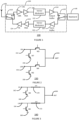
- FIG. 1 Shows an example 5G RF system 100 for a mobile device or a base station.
- a 5G system typically utilises higher frequency bands for example at frequencies in the region of 28 GHz and 39 GHz.
- 5G systems typically exploit beamforming techniques to steer the RF energy to where it is required. By steering the RF energy, the amount of power required may be reduced and furthermore steering the RF energy may also help prevent spectral pollution. Beamforming typically requires multiple antennas and consequently multiple RF front ends.
- the 5GRF system 100 may include an antenna 102, an RF channel 130, and a baseband circuit 140.
- the baseband circuit 140 may include RF mixers and other analog and/or digital circuitry.
- the 5G RF system 100 is illustrated showing one RF front end channel 130, and one antenna 102, but it will be appreciated that multiple channels and antennas will be used in a typical 5G system.
- the RF channel 130 may include a first RF SPDT switch 110 having a common connection to the antenna 102.
- the RF channel 130 may include a second RF SPDT switch 120 having a common connection to baseband circuit 140.
- the RF channel 130 further includes a receive path which may consist of a series arrangement of a low noise amplifier (LNA) 106, a variable gain amplifier (VGA) 108, a vector modulator 112, and an output buffer 114 connected between the first RF switch 110 and the second RF switch 120.
- the RF channel 130 further includes a transmit path which may consist of a series arrangement of an input buffer 116 a vector modulator 118, a variable gain amplifier 122, and a power amplifier 124 connected between the second RF switch 120 and the first RF switch 110.
- the first RF switch 110 may also be referred to as an antenna switch.
- the first RF switch 110 and the second RF switch 120 are controlled by a control circuit (not shown) to select the transmit path.
- the baseband circuit 140 is connected to the input of the input buffer 116 via the second RF switch 120, and the output of the power amplifier 124 is connected to the antenna 102 via the first RF switch 110.
- the first RF switch 110 and the second RF switch 120 are controlled by a control circuit (not shown) to select the receive path.
- the antenna 102 is connected to the input of the low noise amplifier 106 via the second RF switch 120 and the output of the output buffer 114 is connected to the baseband circuit 140 via the first RF switch 110.
- further switches may be used to combine multiple receive output signals from output buffers in the receive mode of operation or to split multiple transmit input signals for each input buffer in a respective channel.
- bandpass filters may be included between the first RF switch 110 and the antenna 102. It is desirable for the RF switches 110, 120 to have a low insertion loss value while still meeting other requirements such as linearity, breakdown voltage performance, switching time, and noise figure.
- FIG. 2 shows a typical RF SPDT antenna switch 150 implemented using n-type MOS transistors.
- MOSFET devices may be implemented for example in a BiCMOS SiGe technology.
- a first NFET M1 has a source connected to a ground potential 158 and a drain connected to a first terminal 152 which may be connected to a power amplifier output (not shown).
- a second NFET M2 has a source connected to the ground potential 158 and a drain connected to a second terminal 154 which may be connected to a low noise amplifier input (not shown).
- a third NFET M3 has a source connected to the first terminal 152 and a drain connected to the antenna terminal 156.
- a fourth NFET M4 has a source connected to the second terminal 154 and a drain connected to the common or antenna terminal 156.
- the gate connections of transistors M1, M2, M3, and M4 are connected to control circuitry (not shown).
- transistors M1 and M4 In operation of the antenna switch 150, in a transmit mode when transistors M2 and M3 are turned on, transistors M1 and M4 will be turned off. In this mode of operation, an antenna connected to the antenna terminal 156 will be connected to the first terminal 152 which may be connected to a power amplifier. In a receive mode of operation, transistors M1 and M4 are turned on and transistors M2 and M3 are turned off. In the receive mode of operation, the second terminal 154 will be connected to the antenna terminal 156 and a low noise amplifier input connected to the second terminal 154 will be able to receive signals from an antenna connected to the antenna terminal 156.
- the antenna switch 150 typically has a relatively high insertion loss which may be approximately 1.5 dB. This insertion loss may be due to the on-resistance of the MOSFET. The insertion loss may also be due to large parasitic capacitances between the MOSFET drain and/or source to the gate and the substrate.
- Figure 3 shows an alternative typical RF SPDT switch 160 that uses transmission lines (TL) to avoid the use of series switches.
- a first NFET M5 has a source connected to a ground potential 168 and a drain connected to a first terminal 162 which may be connected to a power amplifier output (not shown).
- a second NFET M6 has a source connected to the ground potential 168 and a drain connected to a second terminal 164 which may be connected to a low noise amplifier input (not shown).
- a first quarter-wavelength ( ⁇ /4) transmission line 170 is connected between the first terminal 162 and the antenna terminal 166.
- a second quarter-wavelength ( ⁇ /4) transmission line 172 is connected between the second terminal 164 and the antenna terminal 166.
- the gate connections of transistors M5 and M6 are connected to control circuitry (not shown).
- the first transistor M5 will be switched off and the second transistor M6 will be switched on.
- the second transmission line 172 will act as an impedance inverter and invert the low on state impedance of the second transistor M6 to an open at the antenna terminal. This enables a RF signal to flow in the branch between the first terminal 162 and the antenna terminal 166.
- the first transistor M5 In a receive mode of operation, the first transistor M5 will be switched on and the second transistor M6 will be switched off.
- the first transmission line 170 will invert the low on state impedance of the first transistor M5 to an open at the antenna. This enables an RF signal to flow in the branch between the second terminal 164 and the antenna terminal 166.
- the RF switch 160 may be used at high frequencies, for example frequencies above 10 GHz. However, the insertion loss may still be relatively high. Furthermore when the transmission lines 170, 172 are implemented as a micro strip line or co-planar waveguide on an integrated circuit. They may be bulky which may result in further losses. When the transmission lines are implemented with lumped elements such as inductors or capacitors, the RF switch 160 may be lossy because of the low Q factor of the on-chip inductors or coils.
- FIG. 4 shows an example RF switch 200.
- a first switchable capacitor 210 is connected between a first terminal 202 and a common terminal 206.
- a second switchable capacitor 220 is connected between a second terminal 204 and the common terminal 206.
- a control circuit 230 which may be considered a bias circuit may have a control input 214.
- the bias circuit 230 may have a first control output 212 connected to the first switchable capacitor 210.
- the bias circuit 230 may have a second control output 208 connected to the second switchable capacitor 220.
- the first switchable capacitor 210 and the second switchable capacitor 220 may be configured in either a blocking state or a pass state determined by a control signal received on the control input 214.
- the received control signal in turn determines the control signals provided to the first switchable capacitor 210 on first control output 212 and the second switchable capacitor 220 on the second control output 208.
- the first terminal 202 may be connected to a power amplifier output (not shown)
- the second terminal 204 may be connected to a low noise amplifier input (not shown)
- the common terminal 206 may be connected to an antenna.
- the switchable capacitors 210,220 may be considered to be in the blocking state or off state when a desired RF signal is substantially blocked from the path between either the first terminal 202 and the common terminal 206 or the second terminal 204 and the common terminal 206.
- the switchable capacitors 210,220 may be considered to be in the pass state or on state when a desired RF signal can pass through the path between either the first terminal 202 and the common terminal 206 or the second terminal 204 and the common terminal 206.
- the bias circuit 230 is configured such that in a first mode of operation the first switchable capacitor 210 is in a blocking state and the second switchable capacitor 220 is in a pass state, and in a second mode of operation the first switchable capacitor 210 is in a pass state and a second switchable capacitor 220 is in a blocking state.
- the bias circuit 230 may be further configured so that both first switchable capacitor 210 and the second switchable capacitor 220 are in a blocking state when neither transmit or receive functionality is required.
- the capacitance of the respective switchable capacitor 210, 220 is relatively small.
- the capacitance of the respective switchable capacitor 210, 220 is relatively large.
- the switchable capacitors 210, 220 may function to couple an AC signal received at one terminal of the switchable capacitor to a second terminal, with very low IL.
- a 1pF capacitor at 28GHz has an impedance of 5.752, but results in a IL value of 0.014dB.
- a resistor of 5.7Q would result in an IL value of 0.5dB.
- a capacitor as pass device no additional noise may be generated which may further improve the noise factor.
- the inventors of the present disclosure have appreciated that by using switchable capacitors rather than the conventional switch topologies, an RF switch for antennas with low IL may be implemented.
- the inventors have further appreciated that the RF switch 200 may in particular be used for systems with higher RF frequencies, for example frequencies above 10 GHz.
- Figure 5 shows an example RF switch 250.
- a first switchable capacitor 260 having diode D1 is connected between a first terminal 252 and a common terminal 256.
- a second switchable capacitor 270 having diode D2 is connected between a second terminal 254 and the common terminal 256.
- a bias circuit 280 may have a control input 264.
- the bias circuit 280 may have a first control output 258 connected to the first terminal 252.
- the bias circuit 280 may have a second control output 262 connected to the second terminal 254.
- the bias circuit 280 may have a third control output 266 connected to the common terminal 256.
- the bias circuit 280 may forward bias diode D1 and reverse bias diode D2 by applying appropriate voltages and/or currents to the control outputs 258, 262, 266.
- the forward bias diode D1 may have a capacitance value much higher than the reverse biased diode D2.
- the first switchable capacitor 260 is configured in an on-state or pass-state and the second switchable capacitor 270 is in an off-state or a blocking-state.
- an RF signal received on the common terminal 256 which might be connected to an antenna (not shown) may be passed via diode D1 to the first terminal 252 which may for example be connected to the input of the low noise amplifier (not shown).
- the bias circuit 218 may reverse bias diode D1 and forward bias diode D2 by applying appropriate voltages and/or currents to the control outputs 258, 262, 266.
- Forward biased diode D2 may have a capacitance value that is much higher than the reverse biased diode D1.
- the first switchable capacitor 260 is configured in an off state or blocking-state and the second switchable capacitor 270 is configured in an on-state or a pass state.
- an RF signal transmitted on the second terminal 254 which might be connected to a power amplifier output (not shown) may be passed via diode D2 to the common terminal 256 which may for example be connected to an antenna (not shown).
- the orientation of the diodes D1, D2 may be in either direction provided the bias circuit 280 provides the appropriate bias voltages and/or currents. This is because the diodes are being used to implement a switchable capacitor rather than the conventional diode function.
- the diodes D1, D2 may be replaced by PiN diodes, varicap devices, or diode connected bipolar transistors.
- Figure 6 shows an RF switch 300 according to an embodiment.
- a first switchable capacitor 310 having a diode-connected reverse transistor Q1 is connected between a first terminal 302 and a common terminal 306.
- a second switchable capacitor 320 having a diode-connected reverse transistor Q2 is connected between a second terminal 304 and the common terminal 306.
- the term diode-connected reverse transistor as used herein refers to a bipolar transistor such as a heterojunction bipolar transistor (HBT) with the base connected to the emitter. Such a transistor is being used in a configuration which is the reverse of the normal transistor operation.
- Q1 and Q2 are shown as NPN transistors. In other examples PNP transistors may be used.
- a bias circuit 330 may have a control input 314.
- the bias circuit 330 may have a first control output 312 connected to a first terminal of a first resonator 322.
- the bias circuit 330 may have a second control output 308 connected to a first terminal of a second resonator 326.
- the bias circuit 330 may have a third control output 316 connected to a first terminal of a third resonator 324.
- a second terminal of the first resonator 322 may be connected to the first terminal 302.
- a second terminal of the second resonator 326 may be connected to the second terminal 304.
- a second terminal of the third resonator 324 may be connected to the common terminal 306.
- the resonators 322, 324, 326 may be implemented as a parallel LC circuit, as self resonating coils or by other circuit techniques.
- the resonators 322, 324,326 may have a relatively high impedance at the required RF frequency for example greater than 10 GHz and a much lower impedance at DC to supply any bias current with low voltage drop.
- the resonators 322, 324, 326 may also suppress out-of-band signals.
- the bias circuit 330 may forward bias the base-collector PN junction of transistor Q1 and reverse bias the base-collector PN junction of transistor Q2 by applying appropriate voltages and/or currents to the control outputs 312, 308, 316.
- the first switchable capacitor 310 is configured in an on-state or pass-state and the second switchable capacitor 320 is in an off-state or a blocking-state.
- an RF signal received on the common terminal 306 which might be connected to an antenna (not shown) may be passed via transistor Q1 to the first terminal 302 which may for example be connected to the input of the low noise amplifier (not shown).
- the bias circuit 330 may reverse bias the base-collector PN junction of transistor Q1 and forward bias the base-collector PN junction of transistor Q2 by applying appropriate voltages and/or currents to the control outputs 312, 308, 316.
- the first switchable capacitor 310 is in an off state or blocking-state and the second switchable capacitor 320 is configured in an on-state or a pass state.
- an RF signal transmitted on the second terminal 304 which might be connected to a power amplifier output (not shown) may be passed via transistor Q2 to the common terminal 306 which may for example be connected to an antenna (not shown).
- Q1 and Q2 are connected to the common terminal 306.
- Q1 and Q2 are being used as switchable capacitances rather than their conventional transistor function, the orientation of Q1 and Q2 is irrelevant provided the appropriate biasing used. Consequently, in other examples, one or both of Q1 and Q2 may be connected in the reverse direction to that shown.
- the breakdown voltage of the collector-base junction of transistors Q1 and Q2 is relatively high. This is especially true if Q1 and Q2 are implemented using a high voltage transistor which may use a collector with lower doping level compared to the high-speed transistor. The lower doping level also results in lower reverse collector-base capacitance which is required in the off-state. A large reverse bias voltage may also lower the collector-base capacitance. Since the off-state device should be able to withstand the potentially large signals of the pass path, a reverse bias voltage of about half the breakdown voltage may be optimal. In this case the maximal negative amplitude will hit the breakdown limit, while the maximal positive amplitude will hit the point where the device cannot maintain its off-state and starts turning on.
- the transit frequency fT of the reverse transistor may be much lower than a forward transistor.
- the reverse transistor may have more than 10x less fT compared to the normal forward transistor. This means that more than 10x less current is needed to get a certain on-state diffusion capacitance.
- the reverse transistor Q1 may be biased in the on-state beyond peak fT, for example at current densities 10x larger compared to current densities that yield maximal fT performance in order to further increase the diffusion capacitance.
- a further benefit of the diode-connected reverse transistors Q1, Q2 is the presence of the emitter. Shorting the emitter to the base may protect the base-emitter junction for reverse voltages. But this does not make the emitter ineffective: the emitter will carry most bias current taking it away from the base by the beta of the reverse transistor. For example, if the reverse beta is 100 with a bias current of 4mA, the base current will be only 40uA. If the emitter was not present, then the full 4mA would be driven into the p-type base. In the vertical structure of the emitter-base-collector NPN device there is a p-type substrate that makes a corresponding parasitic vertical PNP structure from the base-collector-substrate. Hence less bias current in the parasitic PNP may result in less injection of current into the substrate. Since substrate currents exhibit broadband noise, this is not only a benefit at DC, but also may improve NF at the operating frequency of the signals switched by the RF switch 300.
- Figure 7A shows the equivalent circuit 350 of the diode-connected reverse transistors Q1 and Q2 in the on-state or pass-state.
- the equivalent circuit 350 consists of a contact resistance Rcontact in series with a parallel arrangement of the diffusion capacitance Cdiff and a resistance 1/gm, where gm is the transconductance derived from the exponential bipolar IV transfer curve, and may be determined from the collector current divided by the thermal voltage kT/q.
- the collector current of transistors Q1 and Q2 is equivalent to the bias current when in the pass-state.
- Figure 7B shows a graph 360 of the on-state resistance Ron taken as real part of the on-state impedance of the forward biased collector base junction as a function of frequency according to the equivalent circuit 350.
- the y-axis 362 shows the on-resistance Ron in ohms varying between zero and 20 ohms.
- the x-axis 364 shows frequency on a logarithmic scale varying between the frequency of hundred megahertz to 100 GHz. Three regions are illustrated. Region 1 varies from a frequency of 100 MHz to approximately 2 GHz marked by dashed line 368. Region 2 varies between dashed line 368 at the value of approximately 2 GHz to dashed line 370 at the value of approximately 40 GHz. Region 3 covers the frequencies above 40 GHz.
- Ron is dominated by the value of 1/gm and is substantially constant.
- the frequency becomes larger than the transit frequency of the transistor and the diffusion capacitance Cdiff starts to dominate more and more resulting in a reduced effective resistance Ron.
- the contact resistance limits any further reduction in the value of the on-state resistance Ron.
- the inventors of the present disclosure have appreciated that the RF signal flows predominantly through the diffusion capacitance and not through the diode conductance. In this way, an RF switch may be implemented having low insertion loss.
- the RF switch 300 may have low noise since the transconductance noise may be short-circuited by the diffusion capacitor.
- the RF switch 300 may have high small-signal linearity resulting in a higher value for the third order intercept point IP3, since the diffusion capacitor is largely constant because there is no modulation of the diode conductance.
- the RF switch 300 may have high large-signal linearity resulting in a higher value for the 1dB compression point because the bias current through the diode conductance is not driven to zero by the RF current.
- FIG 8A shows an RF switch 400 according to an embodiment.
- a first switchable capacitor 410 having a diode-connected reverse transistor Q1a is connected between a first terminal 402 and a common terminal 406.
- a second switchable capacitor 420 having a diode-connected reverse transistor Q2a is connected between a second terminal 404 and the common terminal 406.
- the term diode-connected reverse transistor as used herein refers to a bipolar transistor such as a heterojunction bipolar transistor (HBT) with the base connected to the emitter. Such a transistor is being used in a configuration which is the reverse of the normal transistor operation.
- Q1a and Q2a are shown as NPN transistors.
- the emitter of Q1a is connected to the first terminal 402.
- the emitter of Q2a is connected to the common terminal 406.
- a bias circuit 430 may have a control input 414.
- the bias circuit 430 may have a first control output 412 connected to a first terminal of a first resonator 422.
- the bias circuit 430 may have a second control output 416 connected to a first terminal of a second resonator 426.
- the bias circuit 430 may have a third control output 418 connected to a first terminal of a third resonator 424.
- a second terminal of the first resonator 422 may be connected to the first terminal 402.
- a second terminal of the second resonator 426 may be connected to the second terminal 404.
- a second terminal of the third resonator 424 may be connected to the common terminal 406.
- the first resonator 422 may include a parallel arrangement of a capacitor C1a and an inductor L1a between the first resonator first terminal and the first resonator second terminal.
- the second resonator 426 may include a parallel arrangement of a capacitor C2a and an inductor L2a between the second resonator first terminal and the second resonator second terminal.
- the third resonator 424 may include a parallel arrangement of a capacitor C3a and an inductor L3a between the third resonator first terminal and the third resonator second terminal.
- Bias circuit 430 may include a first switchable current source SI1 arranged between the supply rail 432 configured to supply a voltage Vcc and the first control output 412.
- the bias circuit 430 may include a first switchable voltage source 442.
- the first switchable voltage source 442 may have an NMOS transistor MN3 with a source connected to a common supply rail 434 which may be a ground, a drain connected to the first control output 412, and a gate connected to node A.
- Bias circuit 430 may include a second switchable current source SI2 arranged between the common supply rail 434 and the second control output 416.
- the bias circuit 430 may include a second switchable voltage source 440.
- the second switchable voltage source 440 may have a PMOS transistor MP3 with a source connected to the supply rail 432, a drain connected to the second control output 416, and a gate connected to node D.
- the bias circuit 430 may include a common switchable voltage source 438.
- the common switchable voltage source 438 may include a series cascode arrangement of a first and second PMOS transistors MP1 and MP2 between the supply rail 432 and the third control output 418.
- the common switchable voltage source 438 may include a series cascode arrangement of a first and second NMOS transistors MN1 and MN2 between the common rail 434 and the third control output 418.
- the gate of first PMOS transistor MP1 may be connected to node B.
- the gates of second PMOS transistor MP2, and second NMOS transistor MN2 may be connected to bias supply rail 436 which may supply a voltage of Vcc/2.
- the gate of first NMOS transistor MN1 may be connected to node C.
- Using a cascode arrangement allows MOS transistors which operate at lower voltages for example 2.5 volts to be used with a higher supply voltage level Vcc, for example 5 volts.
- the cascode arrangement may be replaced by a single PMOS and NMOS transistor.
- the bias circuit 430 does not require a charge pump to generate negative voltages or voltages larger than Vcc.
- the bias circuit 430 may include a bias control 444 having an input connected to the control input 414 which may be a control bus.
- the bias control 444 may be connected to supply rail 432, bias supply 436 and common rail 434.
- the bias control 444 may have four outputs connected to nodes A, B, C, D respectively.
- the bias circuit 430 may forward bias the base-collector PN junction of transistor Q1a and reverse bias the base-collector PN junction of transistor Q2a by applying a forward current to Q1a and a reverse voltage to Q2a.
- the first switchable capacitor 410 is configured in an on-state or pass-state and the second switchable capacitor 420 is in an off-state or a blocking-state.
- an RF signal received on the common terminal 406 which might be connected to an antenna (not shown) may be passed via transistor Q1a to the first terminal 402 which may for example be connected to the input of the low noise amplifier (not shown).
- the bias current is supplied by the first switchable bias current source SI1.
- the second switchable bias source SI2 is switched off by some means of control (not shown).
- the reverse bias voltage may be generated by the switchable voltage sources 438, 440, 442 under control of the bias control 444.
- the bias circuit 430 may reverse bias the base-collector PN junction of transistor Q1a and forward bias the base-collector PN junction of transistor Q2a by applying a reverse voltage to Q1a and a forward current to Q1b.
- the first switchable capacitor 410 is in an off state or blocking-state and the second switchable capacitor 420 is configured in an on-state or a pass state.
- an RF signal transmitted on the second terminal 404 which might be connected to a power amplifier output (not shown) may be passed via transistor Q2a to the common terminal 406 which may for example be connected to an antenna (not shown).
- the bias current is supplied by the second switchable bias current source SI2.
- the first switchable bias current source SI1 is switched off.
- the reverse bias voltage may be generated by the switchable voltage sources 438, 440, 442 under control of the bias control 444.
- first terminal 402 or second terminal 404 can be connected to a LNA or PA.
- the bias control 444 may generate voltages on each of the output nodes A, B, C and D as indicated in table 1 for the first mode and the second mode. It will be appreciated that the circuitry of bias control 444 may for example be implemented as an analog multiplexer controlled by the control input 414.
- the RF switch 400 may be used to implement switchable capacitors with a blocking or off-state capacitance value for example of Coff of approximately 12fF and a pass or on-state capacitance value Con of approximately 3pF at a few milliamps of bias current.
- the LC parallel resonators 422, 424, 426 may exhibit high impedance at the required 5G frequencies, and low impedance at DC to enable passing current with low voltage drop. Hence, the resonators 422, 424, 426 may isolate the bias circuitry 430 from the RF signal path which runs from either first terminal 402 or second terminal 404 to the common terminal 406.
- the output impedance of the current sources SI1 and SI2 in the bias circuitry 430 may not be high enough at the RF signal frequencies. This may result in the current sources loading the RF signal path and so reducing the insertion loss.
- the insertion loss may be reduced.
- the LC resonators 422,424, 426 may also add selectivity which may be desired to suppress out-of-band signals.
- the resonators 422,424,426 may be implemented as self-resonating coils. In a self-resonating coil, the parallel C is parasitic of the coil structure. Using LC resonators rather than an inductance alone may reduce the size of the required inductance coil.
- the RF switch 400 allows the full supply voltage Vcc to be used as reverse blocking voltage for the junction. This gives minimal off-state capacitance and may be an optimal voltage relative to breakdown voltages of 2xVcc which may be approximately 10V.
- FIG 8B shows an example implementation of a switchable current source 450 which may be used to implement current source SI1 in the RF switch 400 shown in figure 8A .
- a series arrangement of a PMOS transistor MP4 and a resistor R1 may be connected between a supply rail 432 and a first control output 412.
- the gate of the PMOS transistor MP4 may be connected to a node D as illustrated in RF switch 400.
- the PMOS transistor MP4 may be controlled by the bias control circuit 444 to provide a bias current in the first mode of operation. It will be appreciated that in other examples, different implementations of switchable current sources may also be used.
- Figure 8C shows an example implementation of a switchable current source 460 which may be used to implement current source SI2 in the RF switch 400 shown in figure 8A .
- a series arrangement of a NMOS transistor MN4 and a resistor R2 may be connected between a common rail 434 and a second control output 416.
- the gate of the NMOS transistor MN4 may be connected to a node A as illustrated in RF switch 400.
- the NMOS transistor MN4 may be controlled by the bias control circuit 444 to provide a bias current in the second mode of operation. It will be appreciated that in other examples, different implementations of switchable current sources may also be used.
- Figure 9A shows an RF switch 500 according to an embodiment.
- a first switchable capacitor 510 having a diode-connected reverse transistor Q1b is connected between a first terminal 502 and a common terminal 506.
- a second switchable capacitor 520 having a diode-connected reverse transistor Q2b is connected between a second terminal 504 and the common terminal 506.
- the term diode-connected reverse transistor as used herein refers to a bipolar transistor such as a heterojunction bipolar transistor (HBT) with the base connected to the emitter.
- HBT heterojunction bipolar transistor
- Q1b and Q2b are shown as NPN transistors. In other examples, PNP transistors, may be used.
- the emitter of Q1b is connected to the common terminal 506.
- the emitter of Q2b is connected to the common terminal 506.
- a bias circuit 530 may have a control input 514.
- the bias circuit 530 may have a first control output 512 connected to a first terminal of a first resonator 522.
- the bias circuit 530 may have a second control output 516 connected to a first terminal of a second resonator 526.
- the bias circuit 530 may have a third control output 518 connected to a first terminal of a third resonator 524.
- a second terminal of the first resonator 522 may be connected to the first terminal 502.
- a second terminal of the second resonator 526 may be connected to the second terminal 504.
- a second terminal of the third resonator 524 may be connected to the common terminal 506.
- the first resonator 522 may include a parallel arrangement of a capacitor C1b and an inductor L1b between the first resonator first terminal and the first resonator second terminal.
- the second resonator 526 may include a parallel arrangement of a capacitor C2b and an inductor L2b between the second resonator first terminal and the second resonator second terminal.
- the third resonator 524 may include a parallel arrangement of a capacitor C3b and an inductor L3b between the third resonator first terminal and the third resonator second terminal.
- Bias circuit 530 may include a current source ICom arranged between the supply rail 532 configured to supply a voltage Vcc and the third control output 518.
- the bias circuit 530 may include a first switchable voltage source 542.
- the first switchable voltage source 542 may include a series arrangement of a first and second PMOS transistors MP1a and MP2a between the supply rail 532 and the first control output 512.
- the first switchable voltage source 542 may include a series arrangement of a first and second NMOS transistors MN1a and MN2a between the common rail 534 and the first control output 512.
- the gate of first PMOS transistor MP1a may be connected to node E.
- the gates of second PMOS transistor MP2a, and second NMOS transistor MN2a may be connected to bias supply rail 536 which may supply a voltage of Vcc/2.
- the gate of first NMOS transistor MN1a may be connected to node F.
- the bias circuit 530 may include a second switchable voltage source 540.
- the second switchable voltage source 540 may include a series cascode arrangement of a first and second PMOS transistors MP1b and MP2b between the supply rail 532 and the second control output 516.
- the second switchable voltage source 540 may include a series cascode arrangement of a first and second NMOS transistors MN1b and MN2b between the common rail 534 and the second control output 516.
- the gate of first PMOS transistor MP1b may be connected to node G.
- the gates of second PMOS transistor MP2b, and second NMOS transistor MN2b may be connected to bias supply rail 536 which may supply a voltage of Vcc/2.
- the gate of first NMOS transistor MN1b may be connected to node H.
- the bias circuit 530 does not require a charge pump to generate negative voltages or voltages larger than Vcc.
- the bias circuit 530 may include a bias control 544 having an input connected to the control input 514 which may be a control bus. Bias control 544 may be connected to supply rail 532, bias supply 536 and common rail 534. The bias control 544 may have four outputs connected to nodes E, F, G, H respectively.
- the current source ICom is always on and results in a voltage at the common terminal 506 of approximately the forward voltage of Q1b or Q2b respectively.
- the bias circuit 530 may forward bias the base-collector PN junction of transistor Q1b and reverse bias the base-collector PN junction of transistor Q2b by applying a forward current to Q1b and a reverse voltage to Q2b.
- the first switchable capacitor 510 is configured in an on-state or pass-state and the second switchable capacitor 520 is in an off-state or a blocking-state.
- an RF signal received on the common terminal 506 which might be connected to an antenna (not shown) may be passed via transistor Q1b to the first terminal 502 which may for example be connected to the input of the low noise amplifier (not shown).
- the bias circuit 530 may reverse bias the base-collector PN junction of transistor Q1b and forward bias the base-collector PN junction of transistor Q2b by applying a forward current to Q2b and a reverse voltage to Q1b.
- the first switchable capacitor 510 is configured in an off-state or blocking-state and the second switchable capacitor 520 is in an on-state or a pass-state.
- an RF signal received on the second terminal 504 which might be connected to a power amplifier (not shown) may be passed via transistor Q2b to the common terminal 506 which may for example be connected to an antenna (not shown).
- the bias control 544 may generate voltages on each of the output nodes E, F, G and H as indicated in table 2 below for the first mode and the second mode. It will be appreciated that the circuitry of bias control 544 may for example be implemented as an analog multiplexer controlled by the control input 514.
- the first terminal 502 is connected to ground 534 via the NMOS transistors MN1a, MN2a and the second terminal 504 is connected to Vcc 532 via PMOS transistors MP1b and MP2b.
- the first terminal 502 is connected to Vcc 532 via the PMOS transistors MP1a, MP2a and the second terminal 504 is connected to ground 534 via NMOS transistors MN1b and MN2b.
- the RF switch 500 may be used for example to implement switchable capacitors with a blocking or off-state capacitance value for example of Coff of approximately 12fF and a pass or on-state capacitance value Con of approximately 3pF at a few milliamps of bias current.
- This RF switch 500 may have a low insertion loss. Since emitters of both Q1b and Q2b are connected to the common terminal 506, noise due to parasitic connections from collector to the substrate in the blocked path is reduced.
- FIG. 9B shows a power adaptive current bias source 550 which may be used for the current source ICOM in RF switch 500.
- the power adaptive current bias source 550 may include a first current mirror formed from NPN bipolar bias transistors QB1 and QB2 and a second current mirror formed using PMOS transistors MB1 and MB2.
- a current reference 552 may be arranged between supply rail 532 and a collector of first bias transistor QB1.
- the first bias transistor QB1 may have a base connected to a first terminal of resistance RB1.
- the first bias transistor QB1 may have an emitter connected to a common rail 534.
- the second terminal of resistance RB1 may be connected to the base 560 of a second bias transistor QB2.
- a first capacitor C1 may be connected between an RF input 562 and the base 560 of the second transistor QB2.
- the RF input 562 may typically be connected to a power amplifier (not shown) that has an output connected to either first terminal 502 or the second terminal 504 of the RF switch 500.
- the RF input 562 may be connected to the input of the final amplifier stage. In other examples, the RF input 562 may be connected to the first terminal 502, the second terminal 504 or the common terminal 506.
- the collector 556 of second bias transistor QB2 may be connected to the gate of first PMOS transistor MB2 and the gate of second PMOS transistor MB2.
- the collector 556 of the second bias transistor QB2 may be connected to a first terminal of second capacitor C2.
- the second terminal of second capacitor C2 may be connected to the supply rail 532.
- the collector 556 of second bias transistor QB2 may be connected to the drain of second PMOS transistor MB2.
- the source of first PMOS transistor MB1 and the source of second PMOS transistor MB2 may be connected to the supply rail 532.
- the drain of first PMOS transistor MB1 may be connected to the second control output 518.
- a reference current Iref provided by the current source 552 may be copied by the current mirror formed from QB1 and QB2 in a ratio determined by the relative dimensions of the two transistors QB1 and QB2.
- transistor QB2 may be dimensioned such that the collector current of QB2 is 10 times the reference current Iref.
- the current provided by QB2 is then copied by the current mirror formed by PMOS transistors MB1 and MB2 to provide a bias current Ibias to the common terminal 506 of the RF switch 500.
- an RF signal received on the RF input 562 may increase the base current of QB2 and consequently increase the collector current of QB2 and therefore the bias current provided by the current mirror formed by PMOS transistors MB1 and MB2.
- the bias current may vary above a minimum quiescent current value depending on the power of the RF signal.
- Low bias currents in general approximately 1mA may be preferred to achieve low power consumption and so reduce the thermal heat of the IC.
- the associated small signal IP3 linearity at approximately 40dBm may be sufficient, but the large signal P1dB compression may not be sufficient at approximately 10dBm at these low bias currents.
- adaptive current bias circuit may also be implemented as a switchable current source and used in other embodiments of RF switches described herein.
- Embodiments described may be used to implement RF switches with a low insertion loss IL which may be approximately 0.5dB or less.
- This IL may be a 1dB improvement on known RF switches.
- a 1dB improvement enables a PA to lower its bias current with more than a few milliamps (mA) because it can drop its maximum Pout with 1dB for the same output power at the antenna.
- This 1dB improvement may also lower the NF of the receiver by 1dB.
- RF SPDT switches implement RF SPDT switches. It will be appreciated that in other examples, different configurations of RF switches may be implemented.
- Embodiments of the RF switches may be included in the RF communication system 100 to replace the SPDT switches 110, 120.
- Embodiments of the RF switches may be used to implement millimetre Wave (mmW) RF switches.
- mmW millimetre Wave
- embodiments of the RF switches may be used in other high frequency wireless applications like 5G Mobile, radar, satellite or dedicated short range communications (DSRC) for automotive operating at frequencies greater than 10 GHz which can benefit from the described methods of achieving a low insertion loss.
- the RF switches described herein may be used at higher bias currents.
Landscapes
- Engineering & Computer Science (AREA)
- Computer Networks & Wireless Communication (AREA)
- Signal Processing (AREA)
- Power Engineering (AREA)
- Amplifiers (AREA)
- Transceivers (AREA)
Claims (13)
- HF-Schalter (200, 250, 300) zum Verbinden einer Antenne mit einer Sende-/Empfangsvorrichtung, wobei der HF-Schalter einen ersten schaltbaren Kondensator (210, 260), der zwischen einem ersten Anschluss (202, 252) und einem gemeinsamen Anschluss (206, 256) in Reihe geschaltet ist, und einen zweiten schaltbaren Kondensator (220, 270), der zwischen einem zweiten Anschluss (204, 254) und dem gemeinsamen Anschluss (206, 256) in Reihe geschaltet ist, umfasst; sowohl der erste als auch der zweite schaltbare Kondensator zwischen einem Durchlasszustand und einem Sperrzustand schaltbar sind und der Kapazitätswert im Durchlasszustand größer als der Kapazitätswert im Sperrzustand ist; wobeisowohl der erste als auch der zweite schaltbare Kondensator (410, 420) einen jeweiligen Bipolartransistor (Q1A, Q2A) umfassen, der eine Basis aufweist, die mit dem Emitter verbunden ist; undder HF-Schalter ferner eine Vorspannungsschaltung (230, 280) umfasst, die eine Steuerungseingabe aufweist und konfiguriert ist, sowohl den ersten als auch den zweiten schaltbaren Kondensator in Reaktion auf ein Steuersignal am Steuerungseingang entweder im Sperrzustand oder im Durchlasszustand vorzuspannen.
- HF-Schalter nach Anspruch 1, der ferner eine erste Resonatorschaltung (322), die an den ersten Anschluss gekoppelt ist, eine zweite Resonatorschaltung (326), die an den zweiten Anschluss gekoppelt ist, und einen dritten Resonator (324), der an den gemeinsamen Anschluss gekoppelt ist, umfasst, wobei die Impedanz jeder Resonatorschaltung bei HF-Frequenzen höher als bei Gleichstrom ist.
- HF-Schalter nach Anspruch 2, wobei die erste, die zweite und die dritte Resonatorschaltung an die Vorspannungsschaltung (330) gekoppelt sind.
- HF-Schalter nach Anspruch 2 oder 3, wobei die erste, die zweite und die dritte Resonatorschaltung Eigenresonanzspulen umfassen.
- HF-Schalter nach einem vorhergehenden Anspruch, wobei die Vorspannungsschaltung (330) konfiguriert ist, im Durchlasszustand einen Vorspannungsdurchlassstrom zu einem jeweiligen schaltbaren Kondensator und im Sperrzustand eine Sperrvorspannung zu einem jeweiligen schaltbaren Kondensator zu liefern.
- HF-Schalter nach einem vorhergehenden Anspruch, wobei die Vorspannungsschaltung (530) eine leistungsabhängige adaptive Stromquelle (550) umfasst, die konfiguriert ist, den Vorspannungsdurchlassstrom in Abhängigkeit von der Leistung des gewünschten HF-Signals zu liefern.
- HF-Schalter (400) nach einem vorhergehenden Anspruch, wobei die Vorspannungsschaltung (430) eine erste schaltbare Stromquelle (SI1), die an den ersten Anschluss (402) gekoppelt ist, eine erste schaltbare Spannungsquelle (442), die an den ersten Anschluss (402) gekoppelt ist, eine zweite schaltbare Stromquelle (SI2), die an den zweiten Anschluss (404) gekoppelt ist, eine zweite schaltbare Spannungsquelle (440), die an den zweiten Anschluss (404) gekoppelt ist, und eine gemeinsame schaltbare Spannungsquelle (438), die an den gemeinsamen Anschluss (406) gekoppelt ist, umfasst und der HF-Schalter konfiguriert ist, in einem ersten Betriebsmodus die erste schaltbare Stromquelle (SI1), die zweite schaltbare Spannungsquelle (440) und die gemeinsame schaltbare Spannungsquelle (438) zu aktivieren, um den ersten schaltbaren Kondensator (410) im Durchlasszustand und den zweiten schaltbaren Kondensator (420) im Sperrzustand zu konfigurieren, und in einem zweiten Betriebsmodus die zweite schaltbare Stromquelle (SI2), die erste schaltbare Spannungsquelle (442) und die gemeinsame schaltbare Spannungsquelle (438) zu aktivieren, um den ersten schaltbaren Kondensator (410) im Sperrzustand und den zweiten schaltbaren Kondensator (420) im Durchlasszustand zu konfigurieren.
- HF-Schalter (400) nach Anspruch 7, wobei der Kollektor des ersten Bipolartransistors (Q1A) und der Emitter des zweiten Bipolartransistors (Q2A) mit dem gemeinsamen Anschluss (406) verbunden sind.
- HF-Schalter (500) nach einem der Ansprüche 1 bis 6, wobei die Vorspannungsschaltung (530) eine Stromquelle (ICom), die an den gemeinsamen Anschluss (506) gekoppelt ist, eine erste schaltbare Spannungsquelle (542), die an den ersten Anschluss(502) gekoppelt ist, und eine zweite schaltbare Spannungsquelle (540), die an den zweiten Anschluss (504) gekoppelt ist, umfasst und der HF-Schalter konfiguriert ist, in einem ersten Betriebsmodus die erste schaltbare Spannungsquelle (542) und die zweite schaltbare Spannungsquelle (540) zu aktivieren, um den ersten schaltbaren Kondensator (510) im Durchlasszustand und den zweiten schaltbaren Kondensator (520) im Sperrzustand zu konfigurieren, und in einem zweiten Betriebsmodus die erste schaltbare Spannungsquelle (542) und die zweite schaltbare Spannungsquelle (540) zu aktivieren, um den ersten schaltbaren Kondensator (510) im Sperrzustand und den zweiten schaltbaren Kondensator (520) im Durchlasszustand zu konfigurieren.
- HF-Schalter nach Anspruch 9, wobei der Emitter des ersten Bipolartransistors (Q1B) und der Emitter des zweiten Bipolartransistors (Q2B) mit dem gemeinsamen Anschluss (506) verbunden sind.
- HF-Schalter nach einem vorhergehenden Anspruch, der als ein SPDT-Schalter konfiguriert ist, wobei der gemeinsame Anschluss konfiguriert ist, an eine Antenne gekoppelt zu sein, der erste Anschluss konfiguriert ist, an einen HF-Verstärkerausgang gekoppelt zu sein, und der zweite Anschluss konfiguriert ist, an einen HF-Verstärkereingang gekoppelt zu sein, und in einem ersten Modus einer des ersten Anschlusses und des zweiten Anschlusses an den gemeinsamen Anschluss gekoppelt ist und in einem zweiten Modus der weitere des ersten Anschlusses und des zweiten Anschlusses an den gemeinsamen Anschluss gekoppelt ist.
- Mobiles Endgerät, das den HF-Schalter nach einem vorhergehenden Anspruch umfasst.
- Sende-/Empfangsvorrichtung, die den HF-Schalter nach einem der Ansprüche 1 bis 11 umfasst.
Priority Applications (3)
| Application Number | Priority Date | Filing Date | Title |
|---|---|---|---|
| EP18154266.3A EP3518426B1 (de) | 2018-01-30 | 2018-01-30 | Hf-schalter |
| US16/253,605 US10862524B2 (en) | 2018-01-30 | 2019-01-22 | RF switch |
| CN201910095216.3A CN110113038B (zh) | 2018-01-30 | 2019-01-30 | Rf开关 |
Applications Claiming Priority (1)
| Application Number | Priority Date | Filing Date | Title |
|---|---|---|---|
| EP18154266.3A EP3518426B1 (de) | 2018-01-30 | 2018-01-30 | Hf-schalter |
Publications (2)
| Publication Number | Publication Date |
|---|---|
| EP3518426A1 EP3518426A1 (de) | 2019-07-31 |
| EP3518426B1 true EP3518426B1 (de) | 2023-04-19 |
Family
ID=61132064
Family Applications (1)
| Application Number | Title | Priority Date | Filing Date |
|---|---|---|---|
| EP18154266.3A Active EP3518426B1 (de) | 2018-01-30 | 2018-01-30 | Hf-schalter |
Country Status (3)
| Country | Link |
|---|---|
| US (1) | US10862524B2 (de) |
| EP (1) | EP3518426B1 (de) |
| CN (1) | CN110113038B (de) |
Families Citing this family (6)
| Publication number | Priority date | Publication date | Assignee | Title |
|---|---|---|---|---|
| CN110365323B (zh) * | 2019-08-28 | 2024-06-07 | 上海爻火微电子有限公司 | TypeC接口的单刀双掷开关电路、模拟开关芯片与电子设备 |
| US11177837B1 (en) * | 2020-06-12 | 2021-11-16 | Apple Inc. | Duplexer with impedance inverters |
| CN113992251B (zh) | 2020-07-09 | 2024-05-14 | 台达电子工业股份有限公司 | 波束成形系统及波束产生器 |
| TWI742755B (zh) * | 2020-07-09 | 2021-10-11 | 台達電子工業股份有限公司 | 波束成形系統及波束產生器 |
| GB2612851B (en) * | 2021-11-16 | 2024-08-21 | Iceye Oy | Radio frequency switch driver |
| EP4344061A1 (de) * | 2022-09-21 | 2024-03-27 | Nxp B.V. | Wilkinson splitter mit zusätzlicher variabler dämpfung und schaltfunktion |
Family Cites Families (17)
| Publication number | Priority date | Publication date | Assignee | Title |
|---|---|---|---|---|
| GB2273423B (en) * | 1992-12-10 | 1997-04-16 | Motorola Gmbh | An antenna switching circuit and method for operating an antenna switch |
| US6434368B1 (en) | 1998-10-27 | 2002-08-13 | Telefonaktiebolaget Lm Ericsson (Publ) | Diode-based switch for a radio transceiver |
| WO2000041326A1 (en) | 1999-01-07 | 2000-07-13 | Motorola Inc. | A radio frequency (rf) switch using a single quarter wave isolating section and method of forming same |
| US6804502B2 (en) * | 2001-10-10 | 2004-10-12 | Peregrine Semiconductor Corporation | Switch circuit and method of switching radio frequency signals |
| US7796969B2 (en) | 2001-10-10 | 2010-09-14 | Peregrine Semiconductor Corporation | Symmetrically and asymmetrically stacked transistor group RF switch |
| US7910993B2 (en) * | 2005-07-11 | 2011-03-22 | Peregrine Semiconductor Corporation | Method and apparatus for use in improving linearity of MOSFET's using an accumulated charge sink |
| CN101484976B (zh) * | 2006-05-02 | 2011-02-23 | Nxp股份有限公司 | 包括改进的电极的电器件及其制造方法 |
| US8044739B2 (en) * | 2009-06-09 | 2011-10-25 | Qualcomm Incorporated | Capacitor switching circuit |
| KR101301213B1 (ko) | 2009-12-16 | 2013-08-28 | 한국전자통신연구원 | 고주파 대역 스위칭용 에스피디티 스위치 |
| KR101301209B1 (ko) | 2009-12-16 | 2013-08-29 | 한국전자통신연구원 | 고주파 대역 스위칭용 씨모오스 스위치 및 스위칭 격리도 강화방법 |
| US9209784B2 (en) * | 2010-04-27 | 2015-12-08 | Rf Micro Devices, Inc. | Switchable capacitive elements for programmable capacitor arrays |
| US9948348B2 (en) * | 2010-05-26 | 2018-04-17 | Skyworks Solutions, Inc. | High isolation switch with notch filter |
| US10461799B2 (en) * | 2012-11-08 | 2019-10-29 | Taiwan Semiconductor Manufacturing Company, Ltd. | Integrated transmitter and receiver front end module, transceiver, and related method |
| EP2940866B1 (de) * | 2014-04-30 | 2021-12-08 | Nxp B.V. | HF-Schalter |
| US9496902B2 (en) * | 2014-07-24 | 2016-11-15 | Skyworks Solutions, Inc. | Apparatus and methods for reconfigurable directional couplers in an RF transceiver with selectable phase shifters |
| US20180048305A1 (en) * | 2016-08-09 | 2018-02-15 | Skyworks Solutions, Inc. | Radio-frequency switch with switchable capacitor |
| US10361697B2 (en) * | 2016-12-23 | 2019-07-23 | Skyworks Solutions, Inc. | Switch linearization by compensation of a field-effect transistor |
-
2018
- 2018-01-30 EP EP18154266.3A patent/EP3518426B1/de active Active
-
2019
- 2019-01-22 US US16/253,605 patent/US10862524B2/en active Active
- 2019-01-30 CN CN201910095216.3A patent/CN110113038B/zh active Active
Also Published As
| Publication number | Publication date |
|---|---|
| CN110113038B (zh) | 2024-09-10 |
| CN110113038A (zh) | 2019-08-09 |
| US10862524B2 (en) | 2020-12-08 |
| US20190238172A1 (en) | 2019-08-01 |
| EP3518426A1 (de) | 2019-07-31 |
Similar Documents
| Publication | Publication Date | Title |
|---|---|---|
| EP3518426B1 (de) | Hf-schalter | |
| EP3547536B1 (de) | System und verfahren zur umgehung eines rauscharmen verstärkers | |
| EP3457577B1 (de) | Verfahren zur herstellung eines asymmetrischen sende-/empfangsschalters mit 90-grad-impedanztransformationsabschnitt | |
| KR100914730B1 (ko) | 무선 단말기 가변이득 저잡음 증폭기 | |
| US12184248B2 (en) | RFFE LNA topology supporting both noncontiguous intraband carrier aggregation and interband carrier aggregation | |
| US8279019B2 (en) | Millimeter-wave switches and attenuators | |
| US8207781B2 (en) | SPDT switch for radio frequency switching and method for enhancing isolation thereof | |
| US10778211B2 (en) | Switching circuit and semiconductor module | |
| US10396714B2 (en) | Reconfigurable low-noise amplifier (LNA) | |
| US8111105B1 (en) | Variable gain BiCMOS amplifier | |
| EP1447906B1 (de) | Rauscharme Verstärker mit Doppelgate-Feldeffekttransistoren | |
| KR100471157B1 (ko) | 증폭기능을 구비한 안테나 스위칭 모듈 | |
| US20240195367A1 (en) | Rf circuit | |
| US10911007B2 (en) | High-frequency amplifier circuitry and semiconductor device | |
| Shiba et al. | F-band bidirectional amplifier using 75-nm InP HEMTs | |
| JP3679400B2 (ja) | 高周波スイッチ、高周波スイッチ・増幅回路、および移動体通信端末 | |
| Do et al. | Design and optimization of a high efficiency 60 GHz SiGe-HBT power amplifier | |
| US20080106331A1 (en) | Switching Low Noise Amplifier | |
| CN120880355A (zh) | 低噪声放大器、射频前端模组及电子设备 | |
| CN119171848A (zh) | 公共输入的低噪声放大器及射频芯片 |
Legal Events
| Date | Code | Title | Description |
|---|---|---|---|
| PUAI | Public reference made under article 153(3) epc to a published international application that has entered the european phase |
Free format text: ORIGINAL CODE: 0009012 |
|
| STAA | Information on the status of an ep patent application or granted ep patent |
Free format text: STATUS: THE APPLICATION HAS BEEN PUBLISHED |
|
| AK | Designated contracting states |
Kind code of ref document: A1 Designated state(s): AL AT BE BG CH CY CZ DE DK EE ES FI FR GB GR HR HU IE IS IT LI LT LU LV MC MK MT NL NO PL PT RO RS SE SI SK SM TR |
|
| AX | Request for extension of the european patent |
Extension state: BA ME |
|
| STAA | Information on the status of an ep patent application or granted ep patent |
Free format text: STATUS: REQUEST FOR EXAMINATION WAS MADE |
|
| 17P | Request for examination filed |
Effective date: 20200131 |
|
| RBV | Designated contracting states (corrected) |
Designated state(s): AL AT BE BG CH CY CZ DE DK EE ES FI FR GB GR HR HU IE IS IT LI LT LU LV MC MK MT NL NO PL PT RO RS SE SI SK SM TR |
|
| STAA | Information on the status of an ep patent application or granted ep patent |
Free format text: STATUS: EXAMINATION IS IN PROGRESS |
|
| 17Q | First examination report despatched |
Effective date: 20210208 |
|
| GRAP | Despatch of communication of intention to grant a patent |
Free format text: ORIGINAL CODE: EPIDOSNIGR1 |
|
| STAA | Information on the status of an ep patent application or granted ep patent |
Free format text: STATUS: GRANT OF PATENT IS INTENDED |
|
| INTG | Intention to grant announced |
Effective date: 20221026 |
|
| GRAJ | Information related to disapproval of communication of intention to grant by the applicant or resumption of examination proceedings by the epo deleted |
Free format text: ORIGINAL CODE: EPIDOSDIGR1 |
|
| STAA | Information on the status of an ep patent application or granted ep patent |
Free format text: STATUS: EXAMINATION IS IN PROGRESS |
|
| GRAP | Despatch of communication of intention to grant a patent |
Free format text: ORIGINAL CODE: EPIDOSNIGR1 |
|
| STAA | Information on the status of an ep patent application or granted ep patent |
Free format text: STATUS: GRANT OF PATENT IS INTENDED |
|
| GRAS | Grant fee paid |
Free format text: ORIGINAL CODE: EPIDOSNIGR3 |
|
| INTC | Intention to grant announced (deleted) | ||
| GRAA | (expected) grant |
Free format text: ORIGINAL CODE: 0009210 |
|
| STAA | Information on the status of an ep patent application or granted ep patent |
Free format text: STATUS: THE PATENT HAS BEEN GRANTED |
|
| INTG | Intention to grant announced |
Effective date: 20230301 |
|
| AK | Designated contracting states |
Kind code of ref document: B1 Designated state(s): AL AT BE BG CH CY CZ DE DK EE ES FI FR GB GR HR HU IE IS IT LI LT LU LV MC MK MT NL NO PL PT RO RS SE SI SK SM TR |
|
| REG | Reference to a national code |
Ref country code: GB Ref legal event code: FG4D |
|
| REG | Reference to a national code |
Ref country code: CH Ref legal event code: EP |
|
| REG | Reference to a national code |
Ref country code: DE Ref legal event code: R096 Ref document number: 602018048477 Country of ref document: DE |
|
| REG | Reference to a national code |
Ref country code: IE Ref legal event code: FG4D |
|
| REG | Reference to a national code |
Ref country code: AT Ref legal event code: REF Ref document number: 1561964 Country of ref document: AT Kind code of ref document: T Effective date: 20230515 |
|
| REG | Reference to a national code |
Ref country code: LT Ref legal event code: MG9D |
|
| REG | Reference to a national code |
Ref country code: NL Ref legal event code: MP Effective date: 20230419 |
|
| P01 | Opt-out of the competence of the unified patent court (upc) registered |
Effective date: 20230725 |
|
| REG | Reference to a national code |
Ref country code: AT Ref legal event code: MK05 Ref document number: 1561964 Country of ref document: AT Kind code of ref document: T Effective date: 20230419 |
|
| PG25 | Lapsed in a contracting state [announced via postgrant information from national office to epo] |
Ref country code: NL Free format text: LAPSE BECAUSE OF FAILURE TO SUBMIT A TRANSLATION OF THE DESCRIPTION OR TO PAY THE FEE WITHIN THE PRESCRIBED TIME-LIMIT Effective date: 20230419 |
|
| PG25 | Lapsed in a contracting state [announced via postgrant information from national office to epo] |
Ref country code: SE Free format text: LAPSE BECAUSE OF FAILURE TO SUBMIT A TRANSLATION OF THE DESCRIPTION OR TO PAY THE FEE WITHIN THE PRESCRIBED TIME-LIMIT Effective date: 20230419 Ref country code: PT Free format text: LAPSE BECAUSE OF FAILURE TO SUBMIT A TRANSLATION OF THE DESCRIPTION OR TO PAY THE FEE WITHIN THE PRESCRIBED TIME-LIMIT Effective date: 20230821 Ref country code: NO Free format text: LAPSE BECAUSE OF FAILURE TO SUBMIT A TRANSLATION OF THE DESCRIPTION OR TO PAY THE FEE WITHIN THE PRESCRIBED TIME-LIMIT Effective date: 20230719 Ref country code: ES Free format text: LAPSE BECAUSE OF FAILURE TO SUBMIT A TRANSLATION OF THE DESCRIPTION OR TO PAY THE FEE WITHIN THE PRESCRIBED TIME-LIMIT Effective date: 20230419 Ref country code: AT Free format text: LAPSE BECAUSE OF FAILURE TO SUBMIT A TRANSLATION OF THE DESCRIPTION OR TO PAY THE FEE WITHIN THE PRESCRIBED TIME-LIMIT Effective date: 20230419 |
|
| PG25 | Lapsed in a contracting state [announced via postgrant information from national office to epo] |
Ref country code: RS Free format text: LAPSE BECAUSE OF FAILURE TO SUBMIT A TRANSLATION OF THE DESCRIPTION OR TO PAY THE FEE WITHIN THE PRESCRIBED TIME-LIMIT Effective date: 20230419 Ref country code: PL Free format text: LAPSE BECAUSE OF FAILURE TO SUBMIT A TRANSLATION OF THE DESCRIPTION OR TO PAY THE FEE WITHIN THE PRESCRIBED TIME-LIMIT Effective date: 20230419 Ref country code: LV Free format text: LAPSE BECAUSE OF FAILURE TO SUBMIT A TRANSLATION OF THE DESCRIPTION OR TO PAY THE FEE WITHIN THE PRESCRIBED TIME-LIMIT Effective date: 20230419 Ref country code: LT Free format text: LAPSE BECAUSE OF FAILURE TO SUBMIT A TRANSLATION OF THE DESCRIPTION OR TO PAY THE FEE WITHIN THE PRESCRIBED TIME-LIMIT Effective date: 20230419 Ref country code: IS Free format text: LAPSE BECAUSE OF FAILURE TO SUBMIT A TRANSLATION OF THE DESCRIPTION OR TO PAY THE FEE WITHIN THE PRESCRIBED TIME-LIMIT Effective date: 20230819 Ref country code: HR Free format text: LAPSE BECAUSE OF FAILURE TO SUBMIT A TRANSLATION OF THE DESCRIPTION OR TO PAY THE FEE WITHIN THE PRESCRIBED TIME-LIMIT Effective date: 20230419 Ref country code: GR Free format text: LAPSE BECAUSE OF FAILURE TO SUBMIT A TRANSLATION OF THE DESCRIPTION OR TO PAY THE FEE WITHIN THE PRESCRIBED TIME-LIMIT Effective date: 20230720 Ref country code: AL Free format text: LAPSE BECAUSE OF FAILURE TO SUBMIT A TRANSLATION OF THE DESCRIPTION OR TO PAY THE FEE WITHIN THE PRESCRIBED TIME-LIMIT Effective date: 20230419 |
|
| PG25 | Lapsed in a contracting state [announced via postgrant information from national office to epo] |
Ref country code: FI Free format text: LAPSE BECAUSE OF FAILURE TO SUBMIT A TRANSLATION OF THE DESCRIPTION OR TO PAY THE FEE WITHIN THE PRESCRIBED TIME-LIMIT Effective date: 20230419 |
|
| PG25 | Lapsed in a contracting state [announced via postgrant information from national office to epo] |
Ref country code: SK Free format text: LAPSE BECAUSE OF FAILURE TO SUBMIT A TRANSLATION OF THE DESCRIPTION OR TO PAY THE FEE WITHIN THE PRESCRIBED TIME-LIMIT Effective date: 20230419 |
|
| REG | Reference to a national code |
Ref country code: DE Ref legal event code: R097 Ref document number: 602018048477 Country of ref document: DE |
|
| PG25 | Lapsed in a contracting state [announced via postgrant information from national office to epo] |
Ref country code: SM Free format text: LAPSE BECAUSE OF FAILURE TO SUBMIT A TRANSLATION OF THE DESCRIPTION OR TO PAY THE FEE WITHIN THE PRESCRIBED TIME-LIMIT Effective date: 20230419 Ref country code: SK Free format text: LAPSE BECAUSE OF FAILURE TO SUBMIT A TRANSLATION OF THE DESCRIPTION OR TO PAY THE FEE WITHIN THE PRESCRIBED TIME-LIMIT Effective date: 20230419 Ref country code: RO Free format text: LAPSE BECAUSE OF FAILURE TO SUBMIT A TRANSLATION OF THE DESCRIPTION OR TO PAY THE FEE WITHIN THE PRESCRIBED TIME-LIMIT Effective date: 20230419 Ref country code: EE Free format text: LAPSE BECAUSE OF FAILURE TO SUBMIT A TRANSLATION OF THE DESCRIPTION OR TO PAY THE FEE WITHIN THE PRESCRIBED TIME-LIMIT Effective date: 20230419 Ref country code: DK Free format text: LAPSE BECAUSE OF FAILURE TO SUBMIT A TRANSLATION OF THE DESCRIPTION OR TO PAY THE FEE WITHIN THE PRESCRIBED TIME-LIMIT Effective date: 20230419 Ref country code: CZ Free format text: LAPSE BECAUSE OF FAILURE TO SUBMIT A TRANSLATION OF THE DESCRIPTION OR TO PAY THE FEE WITHIN THE PRESCRIBED TIME-LIMIT Effective date: 20230419 |
|
| PLBE | No opposition filed within time limit |
Free format text: ORIGINAL CODE: 0009261 |
|
| STAA | Information on the status of an ep patent application or granted ep patent |
Free format text: STATUS: NO OPPOSITION FILED WITHIN TIME LIMIT |
|
| 26N | No opposition filed |
Effective date: 20240122 |
|
| PG25 | Lapsed in a contracting state [announced via postgrant information from national office to epo] |
Ref country code: SI Free format text: LAPSE BECAUSE OF FAILURE TO SUBMIT A TRANSLATION OF THE DESCRIPTION OR TO PAY THE FEE WITHIN THE PRESCRIBED TIME-LIMIT Effective date: 20230419 |
|
| PG25 | Lapsed in a contracting state [announced via postgrant information from national office to epo] |
Ref country code: SI Free format text: LAPSE BECAUSE OF FAILURE TO SUBMIT A TRANSLATION OF THE DESCRIPTION OR TO PAY THE FEE WITHIN THE PRESCRIBED TIME-LIMIT Effective date: 20230419 Ref country code: IT Free format text: LAPSE BECAUSE OF FAILURE TO SUBMIT A TRANSLATION OF THE DESCRIPTION OR TO PAY THE FEE WITHIN THE PRESCRIBED TIME-LIMIT Effective date: 20230419 |
|
| PG25 | Lapsed in a contracting state [announced via postgrant information from national office to epo] |
Ref country code: MC Free format text: LAPSE BECAUSE OF FAILURE TO SUBMIT A TRANSLATION OF THE DESCRIPTION OR TO PAY THE FEE WITHIN THE PRESCRIBED TIME-LIMIT Effective date: 20230419 |
|
| PG25 | Lapsed in a contracting state [announced via postgrant information from national office to epo] |
Ref country code: MC Free format text: LAPSE BECAUSE OF FAILURE TO SUBMIT A TRANSLATION OF THE DESCRIPTION OR TO PAY THE FEE WITHIN THE PRESCRIBED TIME-LIMIT Effective date: 20230419 |
|
| REG | Reference to a national code |
Ref country code: CH Ref legal event code: PL |
|
| PG25 | Lapsed in a contracting state [announced via postgrant information from national office to epo] |
Ref country code: LU Free format text: LAPSE BECAUSE OF NON-PAYMENT OF DUE FEES Effective date: 20240130 |
|
| GBPC | Gb: european patent ceased through non-payment of renewal fee |
Effective date: 20240130 |
|
| PG25 | Lapsed in a contracting state [announced via postgrant information from national office to epo] |
Ref country code: LU Free format text: LAPSE BECAUSE OF NON-PAYMENT OF DUE FEES Effective date: 20240130 |
|
| PG25 | Lapsed in a contracting state [announced via postgrant information from national office to epo] |
Ref country code: GB Free format text: LAPSE BECAUSE OF NON-PAYMENT OF DUE FEES Effective date: 20240130 |
|
| PG25 | Lapsed in a contracting state [announced via postgrant information from national office to epo] |
Ref country code: BE Free format text: LAPSE BECAUSE OF NON-PAYMENT OF DUE FEES Effective date: 20240131 |
|
| PG25 | Lapsed in a contracting state [announced via postgrant information from national office to epo] |
Ref country code: CH Free format text: LAPSE BECAUSE OF NON-PAYMENT OF DUE FEES Effective date: 20240131 |
|
| PG25 | Lapsed in a contracting state [announced via postgrant information from national office to epo] |
Ref country code: GB Free format text: LAPSE BECAUSE OF NON-PAYMENT OF DUE FEES Effective date: 20240130 Ref country code: CH Free format text: LAPSE BECAUSE OF NON-PAYMENT OF DUE FEES Effective date: 20240131 Ref country code: BE Free format text: LAPSE BECAUSE OF NON-PAYMENT OF DUE FEES Effective date: 20240131 |
|
| REG | Reference to a national code |
Ref country code: BE Ref legal event code: MM Effective date: 20240131 |
|
| PG25 | Lapsed in a contracting state [announced via postgrant information from national office to epo] |
Ref country code: BG Free format text: LAPSE BECAUSE OF FAILURE TO SUBMIT A TRANSLATION OF THE DESCRIPTION OR TO PAY THE FEE WITHIN THE PRESCRIBED TIME-LIMIT Effective date: 20230419 |
|
| PG25 | Lapsed in a contracting state [announced via postgrant information from national office to epo] |
Ref country code: BG Free format text: LAPSE BECAUSE OF FAILURE TO SUBMIT A TRANSLATION OF THE DESCRIPTION OR TO PAY THE FEE WITHIN THE PRESCRIBED TIME-LIMIT Effective date: 20230419 |
|
| PG25 | Lapsed in a contracting state [announced via postgrant information from national office to epo] |
Ref country code: IE Free format text: LAPSE BECAUSE OF NON-PAYMENT OF DUE FEES Effective date: 20240130 |
|
| PG25 | Lapsed in a contracting state [announced via postgrant information from national office to epo] |
Ref country code: IE Free format text: LAPSE BECAUSE OF NON-PAYMENT OF DUE FEES Effective date: 20240130 |
|
| PG25 | Lapsed in a contracting state [announced via postgrant information from national office to epo] |
Ref country code: CY Free format text: LAPSE BECAUSE OF FAILURE TO SUBMIT A TRANSLATION OF THE DESCRIPTION OR TO PAY THE FEE WITHIN THE PRESCRIBED TIME-LIMIT; INVALID AB INITIO Effective date: 20180130 |
|
| PG25 | Lapsed in a contracting state [announced via postgrant information from national office to epo] |
Ref country code: HU Free format text: LAPSE BECAUSE OF FAILURE TO SUBMIT A TRANSLATION OF THE DESCRIPTION OR TO PAY THE FEE WITHIN THE PRESCRIBED TIME-LIMIT; INVALID AB INITIO Effective date: 20180130 |
|
| PG25 | Lapsed in a contracting state [announced via postgrant information from national office to epo] |
Ref country code: TR Free format text: LAPSE BECAUSE OF FAILURE TO SUBMIT A TRANSLATION OF THE DESCRIPTION OR TO PAY THE FEE WITHIN THE PRESCRIBED TIME-LIMIT Effective date: 20230419 |
|
| PGFP | Annual fee paid to national office [announced via postgrant information from national office to epo] |
Ref country code: FR Payment date: 20251217 Year of fee payment: 9 |
|
| PGFP | Annual fee paid to national office [announced via postgrant information from national office to epo] |
Ref country code: DE Payment date: 20251217 Year of fee payment: 9 |