EP3520132B1 - Struktur mit einzelkristallhalbleiterinseln und verfahren zur herstellung solch einer struktur - Google Patents
Struktur mit einzelkristallhalbleiterinseln und verfahren zur herstellung solch einer struktur Download PDFInfo
- Publication number
- EP3520132B1 EP3520132B1 EP17783928.9A EP17783928A EP3520132B1 EP 3520132 B1 EP3520132 B1 EP 3520132B1 EP 17783928 A EP17783928 A EP 17783928A EP 3520132 B1 EP3520132 B1 EP 3520132B1
- Authority
- EP
- European Patent Office
- Prior art keywords
- islands
- layer
- dielectric layer
- monocrystalline semiconductor
- semiconductor islands
- Prior art date
- Legal status (The legal status is an assumption and is not a legal conclusion. Google has not performed a legal analysis and makes no representation as to the accuracy of the status listed.)
- Active
Links
Images

Classifications
-
- H—ELECTRICITY
- H10—SEMICONDUCTOR DEVICES; ELECTRIC SOLID-STATE DEVICES NOT OTHERWISE PROVIDED FOR
- H10P—GENERIC PROCESSES OR APPARATUS FOR THE MANUFACTURE OR TREATMENT OF DEVICES COVERED BY CLASS H10
- H10P14/00—Formation of materials, e.g. in the shape of layers or pillars
- H10P14/20—Formation of materials, e.g. in the shape of layers or pillars of semiconductor materials
- H10P14/27—Formation of materials, e.g. in the shape of layers or pillars of semiconductor materials using selective deposition, e.g. simultaneous growth of monocrystalline and non-monocrystalline semiconductor materials
- H10P14/271—Formation of materials, e.g. in the shape of layers or pillars of semiconductor materials using selective deposition, e.g. simultaneous growth of monocrystalline and non-monocrystalline semiconductor materials characterised by the preparation of substrate for selective deposition
- H10P14/274—Formation of materials, e.g. in the shape of layers or pillars of semiconductor materials using selective deposition, e.g. simultaneous growth of monocrystalline and non-monocrystalline semiconductor materials characterised by the preparation of substrate for selective deposition using seed materials
-
- H—ELECTRICITY
- H10—SEMICONDUCTOR DEVICES; ELECTRIC SOLID-STATE DEVICES NOT OTHERWISE PROVIDED FOR
- H10P—GENERIC PROCESSES OR APPARATUS FOR THE MANUFACTURE OR TREATMENT OF DEVICES COVERED BY CLASS H10
- H10P14/00—Formation of materials, e.g. in the shape of layers or pillars
- H10P14/20—Formation of materials, e.g. in the shape of layers or pillars of semiconductor materials
- H10P14/27—Formation of materials, e.g. in the shape of layers or pillars of semiconductor materials using selective deposition, e.g. simultaneous growth of monocrystalline and non-monocrystalline semiconductor materials
- H10P14/271—Formation of materials, e.g. in the shape of layers or pillars of semiconductor materials using selective deposition, e.g. simultaneous growth of monocrystalline and non-monocrystalline semiconductor materials characterised by the preparation of substrate for selective deposition
-
- H—ELECTRICITY
- H10—SEMICONDUCTOR DEVICES; ELECTRIC SOLID-STATE DEVICES NOT OTHERWISE PROVIDED FOR
- H10P—GENERIC PROCESSES OR APPARATUS FOR THE MANUFACTURE OR TREATMENT OF DEVICES COVERED BY CLASS H10
- H10P14/00—Formation of materials, e.g. in the shape of layers or pillars
- H10P14/20—Formation of materials, e.g. in the shape of layers or pillars of semiconductor materials
- H10P14/29—Formation of materials, e.g. in the shape of layers or pillars of semiconductor materials characterised by the substrates
- H10P14/2901—Materials
- H10P14/2902—Materials being Group IVA materials
- H10P14/2905—Silicon, silicon germanium or germanium
-
- H—ELECTRICITY
- H10—SEMICONDUCTOR DEVICES; ELECTRIC SOLID-STATE DEVICES NOT OTHERWISE PROVIDED FOR
- H10P—GENERIC PROCESSES OR APPARATUS FOR THE MANUFACTURE OR TREATMENT OF DEVICES COVERED BY CLASS H10
- H10P14/00—Formation of materials, e.g. in the shape of layers or pillars
- H10P14/20—Formation of materials, e.g. in the shape of layers or pillars of semiconductor materials
- H10P14/29—Formation of materials, e.g. in the shape of layers or pillars of semiconductor materials characterised by the substrates
- H10P14/2901—Materials
- H10P14/2921—Materials being crystalline insulating materials
-
- H—ELECTRICITY
- H10—SEMICONDUCTOR DEVICES; ELECTRIC SOLID-STATE DEVICES NOT OTHERWISE PROVIDED FOR
- H10P—GENERIC PROCESSES OR APPARATUS FOR THE MANUFACTURE OR TREATMENT OF DEVICES COVERED BY CLASS H10
- H10P14/00—Formation of materials, e.g. in the shape of layers or pillars
- H10P14/20—Formation of materials, e.g. in the shape of layers or pillars of semiconductor materials
- H10P14/32—Formation of materials, e.g. in the shape of layers or pillars of semiconductor materials characterised by intermediate layers between substrates and deposited layers
- H10P14/3202—Materials thereof
- H10P14/3238—Materials thereof being insulating materials
-
- H—ELECTRICITY
- H10—SEMICONDUCTOR DEVICES; ELECTRIC SOLID-STATE DEVICES NOT OTHERWISE PROVIDED FOR
- H10P—GENERIC PROCESSES OR APPARATUS FOR THE MANUFACTURE OR TREATMENT OF DEVICES COVERED BY CLASS H10
- H10P14/00—Formation of materials, e.g. in the shape of layers or pillars
- H10P14/20—Formation of materials, e.g. in the shape of layers or pillars of semiconductor materials
- H10P14/34—Deposited materials, e.g. layers
- H10P14/3402—Deposited materials, e.g. layers characterised by the chemical composition
- H10P14/3404—Deposited materials, e.g. layers characterised by the chemical composition being Group IVA materials
- H10P14/3411—Silicon, silicon germanium or germanium
-
- H—ELECTRICITY
- H10—SEMICONDUCTOR DEVICES; ELECTRIC SOLID-STATE DEVICES NOT OTHERWISE PROVIDED FOR
- H10P—GENERIC PROCESSES OR APPARATUS FOR THE MANUFACTURE OR TREATMENT OF DEVICES COVERED BY CLASS H10
- H10P14/00—Formation of materials, e.g. in the shape of layers or pillars
- H10P14/20—Formation of materials, e.g. in the shape of layers or pillars of semiconductor materials
- H10P14/34—Deposited materials, e.g. layers
- H10P14/3402—Deposited materials, e.g. layers characterised by the chemical composition
- H10P14/3414—Deposited materials, e.g. layers characterised by the chemical composition being group IIIA-VIA materials
- H10P14/3416—Nitrides
-
- H—ELECTRICITY
- H10—SEMICONDUCTOR DEVICES; ELECTRIC SOLID-STATE DEVICES NOT OTHERWISE PROVIDED FOR
- H10P—GENERIC PROCESSES OR APPARATUS FOR THE MANUFACTURE OR TREATMENT OF DEVICES COVERED BY CLASS H10
- H10P14/00—Formation of materials, e.g. in the shape of layers or pillars
- H10P14/20—Formation of materials, e.g. in the shape of layers or pillars of semiconductor materials
- H10P14/34—Deposited materials, e.g. layers
- H10P14/3451—Structure
- H10P14/3452—Microstructure
- H10P14/3458—Monocrystalline
-
- Y—GENERAL TAGGING OF NEW TECHNOLOGICAL DEVELOPMENTS; GENERAL TAGGING OF CROSS-SECTIONAL TECHNOLOGIES SPANNING OVER SEVERAL SECTIONS OF THE IPC; TECHNICAL SUBJECTS COVERED BY FORMER USPC CROSS-REFERENCE ART COLLECTIONS [XRACs] AND DIGESTS
- Y02—TECHNOLOGIES OR APPLICATIONS FOR MITIGATION OR ADAPTATION AGAINST CLIMATE CHANGE
- Y02E—REDUCTION OF GREENHOUSE GAS [GHG] EMISSIONS, RELATED TO ENERGY GENERATION, TRANSMISSION OR DISTRIBUTION
- Y02E10/00—Energy generation through renewable energy sources
- Y02E10/50—Photovoltaic [PV] energy
- Y02E10/544—Solar cells from Group III-V materials
Definitions
- the present invention relates to a structure comprising monocrystalline semiconductor islands arranged on a support.
- the structure is intended to receive an active layer of III-V materials or a stack of such active layers, constituting (s) of a semiconductor device, such as a light-emitting diode.
- islands of single crystal semiconductors are formed in a continuous film of material to release the stress originally present in that film, by deformation during a relaxation treatment.
- relaxed or partially relaxed islets are formed without excessive deformations by warping (“buckling” according to the English expression usually employed), insofar as the islets have sufficiently small dimensions.
- Island formation and relaxation treatment can be performed while the continuous film is disposed on the dielectric layer and the support of the substrate.
- the formation of islets and the treatment of relaxation can be achieved while the continuous film resides on an intermediate support, from which the relaxed or partially relaxed islands will be transferred to the dielectric layer covering the support and thus form the substrate.
- the islands are advantageously made of germanium, SiGe, a III-N material of general formula InAlGaN or any other material which does not commonly exist in massive form.
- the islands may be intended to receive an active layer of III-V materials, or a stack of such layers, semiconductor (s) and crystalline (s) constituting a semi-conductive device.
- -driver They may for example be monocrystalline active layers constituting the quantum wells of a light-emitting diode, or the photo-generating layers of a photovoltaic cell. Reference may be made in this regard to the document US2015155331 .
- the parameters of the growth equipment (such as, for example, the uniformity of the precursor flows, the temperature and the partial pressure prevailing in the deposition chamber) affecting the constitution and the deposition chamber are controlled with very high precision. uniformity of active layers.
- an active layer of III-V material formed on the islands of an “island” substrate could have a non-uniform thickness, greater on the edges of the islands than 'in their centers. This is particularly the case when growth of an active layer of InGaN on relaxed or partially relaxed islets of InGaN. This extra thick peripheral zone cannot be exploited, which limits the useful surface of the islands.
- the dimensions of the islands cannot always be freely chosen to compensate for this unusable peripheral zone. Indeed, these dimensions can be imposed to allow relaxation of the islands without excessive warping.
- the useful surface area of the island is therefore necessarily limited, which does not make it possible to form semiconductor components of large dimensions and which limits the value of these substrates.
- the present invention aims to overcome all or part of the aforementioned drawbacks. It aims in particular to provide an “island” substrate for the production of at least one active layer of uniform thickness.
- the object of the invention proposes a structure for the production of at least one active layer of III-V material comprising a substrate formed of a support having a face main, a dielectric layer disposed on the main face of the support, and a plurality of single crystal semiconductor islands disposed directly on the dielectric layer, the islands having an upper surface to serve as a seed for the growth of the layer active.
- the structure comprises a tie layer having a polycrystalline AlN surface arranged between the monocrystalline semiconductor islands, directly on the portion of the dielectric layer which is not covered by the islands, without masking the surface. area top of the islands, so that the dielectric layer is no longer exposed to its surroundings.
- the structure according to the invention is intended to receive, by growth, at least one active layer.
- the applicant has observed that certain constituent species of the active layer, in particular when the latter was made of III-V material, could lack chemical affinity with the dielectric of the dielectric layer and therefore could not s 'fix it. These species are then likely to migrate, during the growth of the active layer, to attach themselves to the edge of the islets, which disturbs the uniformity of thickness of the active layer which forms on the islets.
- the structure of the invention makes it possible to prevent this phenomenon and to form a particularly uniform active layer.
- the invention also provides a method of making a structure, the method comprising providing a substrate formed of a support having a main face, a dielectric layer disposed over the entire main face of the support, and a plurality of monocrystalline semiconductor islands arranged directly on the dielectric layer, the islands having an upper surface to serve as a seed for the growth of an active layer of III-V material.
- the method comprises forming a tie layer having a polycrystalline AlN surface on the portion of the dielectric layer which is not covered by the islands, without masking the upper surface of the islands, so that the dielectric layer is no longer exposed to its environment.
- the invention also relates to a method for producing a semiconductor device comprising the provision of a structure in accordance with the invention and the formation of at least one active layer of III-V material on the islands of semiconductors. monocrystalline.
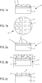
- the figures 1a and 1b schematically show a sectional view from above of a structure 10 according to the invention.
- the structure 10 may have the shape of a circular plate of standardized size, for example 2 inches (50 mm), 4 inches (100 mm) or even 200 mm in diameter. But the invention is in no way limited to these dimensions or to this shape.
- the structure 10 comprises a support 2, for example made of silicon or of sapphire.
- the support 2 has a main face.
- a dielectric layer 3 is placed on the main surface of the support 2.
- the dielectric layer 3 can be made of silicon dioxide, of silicon nitride, or of a single or multiple stack of layers made, for example, of these materials.
- the dielectric layer 3 can have a thickness between 10 nm and several microns.
- the structure 10 also comprises, directly on the dielectric layer 3, a plurality of monocrystalline semiconductor islands 4 (more simply referred to as “islands” in the remainder of the description).
- the term “plurality of islands” denotes a film formed of a set of independent and non-contiguous zones, these zones possibly being delimited by trenches exposing the dielectric layer 3 as is apparent on the figure. figure 1b .
- the islands can all have sizes and / or shapes that are identical or different from one another.
- the invention is in no way limited to islets 4 of a particular nature, but the structure 10 finds a particularly advantageous application when these islets consist of a III-V material, in particular InGaN, relaxed or partially relaxed. .
- the InGaN material may contain a proportion of indium of between 1% and 10%.
- Each island can have a thickness between 100 nm and 200nm, and have a main dimension (diameter or length depending on the shape of the island) between a few microns and 1 mm.
- the islands 4 can be separated from each other by trenches the width of which can be between 1 and 50 microns, and leading to expose the dielectric layer to its environment.
- the structure 10 also comprises between the islands 4, directly on the dielectric layer 3, a tie layer 5.
- This tie layer 5 is placed directly on the portion of the dielectric layer 3 which is not not covered by the islands 4, so that this dielectric layer 3 is no longer directly exposed to its environment.
- the tie layer 5 does not mask the upper surface of the islands 4 so that these surfaces can serve as a seed for the growth of the active layer (or of the stack of active layers).
- the nature of the tie layer 5 is chosen to have sufficient chemical affinity with all the constituent elements of the active layer which will be formed on the structure 10. The tie layer 5 is therefore capable of fixing these elements and preventing their occurrence. migrations during the formation of an active layer.
- the tie layer (5) by its nature and its arrangement, makes it possible to limit the transport of material, typically the diffusion of adatoms, from the surface of the tie layer (5). towards the surface of the islands (4) or of the active layer (6) which is formed on these islands.
- the structure 10, and in particular the islands 4, is intended to receive an active layer comprising a III-V material
- the grip layer 5 is made of AlN. It is formed by depositing directly on the dielectric layer 3 and the bond layer 5 is polycrystalline.
- the thickness of the tie layer 5 is not particularly critical, since only the nature of its exposed surface is used in the context of the present invention.
- the tie layer can be made up of a plurality of layers stacked on top of each other, and only the layer whose surface exposed to the environment requires to have a chemical affinity with the constituent elements of the layer. active. In practice, this thickness will be sufficient to perfectly cover the dielectric layer 3 between the islands 4, while remaining of a thickness less than or equal to that of the islands 4 in order to keep their exposed surfaces projecting and promote the subsequent formation of the active layer.
- the tie layer 5 may have a thickness of between a few nm and a few hundred nm.
- the figure 2 shows a method for producing a semiconductor device taking advantage of the structure 10 which has just been described.
- a structure 10 according to the invention is provided.
- the structure 10 can be placed in the chamber 11 of conventional growth equipment.
- the chamber is traversed by flows of precursor gases, transporting the constituent species of the active layer, and brought to temperature.
- the species included in the precursor gases circulating in the chamber 11 react with the exposed surfaces of the structure 10.
- a monocrystalline active layer 6 gradually forms by epitaxy.
- the good chemical affinity between the tie layer 5 and all the constituent species of the active layer 6 also leads to the formation of a layer 6 ′ between the islands 4, on the tie layer 5. This avoids certain species do not migrate and settle on the edges of the exposed islet surface as is the case in the absence of tie layer 5.
- an active layer 6 can have a uniformity similar to that of the islands on which it has been formed.
- a residue layer 6 ' which may be polycrystalline, has formed.
- This layer of residues 6 ' is not particularly useful and can be eliminated, by conventional steps of masking the useful layer 6 with a photosensitive resin, photolithographic exposure, and dry or wet etching of the layer 6'.
- the (or the active layers) 6 disposed on the structure 10 can undergo additional treatments, well known per se, such as the formation of additional layers, the formation of electrical contacts, the transfer to a final substrate so as to complete the production of the semiconductor device and make it functional.
- the figure 3 shows the steps in the production of a structure 10 according to the invention according to a first embodiment.
- a substrate 1 comprising a support 2, which has a main face, a dielectric layer 3 over the entire main face of the support 2 and a plurality of crystalline semiconductor islands 4 arranged directly on the dielectric layer 3.
- a tie layer 5, 5 ′ is formed over the entire exposed surface of the substrate 1. A portion of the tie layer 5 ′ is placed on the islands 4, and a complementary portion of the tie layer 5 is placed between the islands 4, directly on the dielectric layer 3.
- a third step one proceeds to the removal of the portion of the tie layer 5 ′ arranged on the islands 4 so as to expose their surface, with a view to the subsequent deposition of an active layer 6 or of a plurality of such layers.
- This removal step can be performed in multiple ways.
- the substrate of the figure 3b in a mechanical-chemical polishing step (CMP of the acronym “Chemical Mechanical Polishing”) so as to selectively remove by mechanical and chemical thinning the portion of the tie layer 5 ′ disposed on the islands 4 of the surface of the substrate.
- CMP mechanical-chemical polishing step
- the portion 5 ′ of the bonding layer placed on the islands 4 is removed by dry or wet etching after having previously and selectively masked the portion of the layer with a protective layer. 5 attaches directly disposed the dielectric layer 3.
- This selective masking can be achieved by the traditional steps of full surface deposition of a resin, the exposure of this resin through a photolithographic mask defining the areas of the resin to be removed, and chemical removal of the resin in these areas.
- the figure 4 shows the steps in the production of a structure 10 according to the invention according to a second embodiment.
- the first step shown on the figure 4a supply of the substrate 1 is identical to that of the first embodiment and the same comments apply.
- a second step represented on the figure 4b , the exposed surface of the islands 4 is selectively masked using a protective layer 7, for example a resin layer.
- This selective masking step can be carried out by a traditional method of full surface deposition of the resin, its exposure through a photolithographic mask. making it possible to define zones corresponding to the islands 4 where the resin must be preserved, and the selective chemical withdrawal of the resin outside these zones.
- the tie layer 5, 5 ′ is formed over the entire exposed surface of the substrate 1. A portion of the tie layer 5 ′ resides on the protective layer 7 masking the islands 4, and another portion of the tie layer 5 is placed directly on the dielectric layer 5, between the islands 4.
- the protective layer 7 and the portion of the tie layer 5 'which resides on the protective layer 7. are removed. This can be obtained for example by dispensing a chemical solution. etching making it possible to selectively eliminate the protective layer 7 and leading to the elimination of the portion of the tie layer 5 '.
- the term “monocrystalline semiconductor” denotes a semiconductor material in crystalline form, in which the crystal mesh is continuous, that is to say that it does not have a grain boundary.
- the crystal may however exhibit defects, or imperfections such as point defects, dislocations, without losing its monocrystalline character.
- the structure 10, in addition to the substrate 2, the dielectric layer 3, the islands 4 and the tie layer 5, may include other layers, for example placed under the dielectric layer 3.
- the dielectric layer 3 it is not necessary for the dielectric layer 3 to cover the entire main surface of the support 2. It can, for example, be placed only on the support 2, between the islands 4, or even on only part of the surface of the support. support 2 included between the islands 4.
- the tie layer 5 is formed at least directly on the dielectric layer 3 capable of being exposed to its environment.
Landscapes
- Recrystallisation Techniques (AREA)
- Crystals, And After-Treatments Of Crystals (AREA)
- Chemical & Material Sciences (AREA)
- Crystallography & Structural Chemistry (AREA)
- Thin Film Transistor (AREA)
- Led Devices (AREA)
Claims (12)
- Struktur (10) zur Herstellung mindestens einer aktiven Schicht (6) aus III-V-Material, umfassend ein Substrat, das aus einem Träger (2) mit einer Hauptfläche, einer dielektrischen Schicht (3), die auf der Hauptfläche des Trägers angeordnet ist, und mehreren monokristallinen Halbleiterinseln (4) gebildet ist, die direkt auf der dielektrischen Schicht (3) angeordnet sind, wobei die Inseln eine obere Oberfläche aufweisen, die als Keim für das Wachstum der aktiven Schicht dient, wobei die Struktur dadurch gekennzeichnet ist, dass sie eine Verbindungsschicht mit einer polykristallinen AIN-Oberfläche (5) umfasst, die zwischen den monokristallinen Halbleiterinseln (4) direkt auf dem Abschnitt der dielektrischen Schicht (3) angeordnet ist, der nicht von den Inseln (4) bedeckt ist, ohne die obere Oberfläche der Inseln (4) zu maskieren, so dass die dielektrische Schicht (3) nicht mehr ihrer Umgebung ausgesetzt ist.
- Strukturen (10) nach dem vorhergehenden Anspruch, wobei der Träger (2) aus Silizium oder Saphir besteht.
- Struktur (10) nach einem der vorhergehenden Ansprüche, wobei die dielektrische Schicht (3) Siliziumoxid und/oder Siliziumnitrid umfasst.
- Struktur (10) nach einem der vorhergehenden Ansprüche, wobei die monokristallinen Halbleiterinseln (4) ein III-V-Material umfassen.
- Struktur (10) nach dem vorhergehenden Anspruch, wobei die monokristallinen Halbleiterinseln (4) aus InGaN hergestellt sind oder InGaN umfassen.
- Verfahren zur Herstellung einer Struktur (10), umfassend das Bereitstellen eines Substrats (1), das aus einem Träger (2) mit einer Hauptfläche, einer dielektrischen Schicht (3), die auf der Hauptfläche des Trägers (2) angeordnet ist, und mehreren monokristallinen Halbleiterinseln (4) gebildet ist, die direkt auf der dielektrischen Schicht (3) angeordnet sind, wobei die Inseln eine obere Oberfläche aufweisen, die als Keim für das Wachstum einer aktiven Schicht aus III-V-Material dient, wobei das Verfahren dadurch gekennzeichnet ist, dass es das Bilden einer Verbindungsschicht mit einer polykristallinen AlN-Oberfläche (3) zwischen den monokristallinen Halbleiterinseln (4) direkt auf dem Abschnitt der dielektrischen Schicht (2) umfasst, der nicht von den Inseln (4) bedeckt ist, ohne die obere Oberfläche der Inseln (4) zu maskieren, so dass die dielektrische Schicht (3) nicht mehr ihrer Umgebung ausgesetzt ist.
- Verfahren nach dem vorhergehenden Anspruch, wobei das Bilden der Haftschicht (5) das Abscheiden der Haftschicht (5, 5') auf und zwischen monokristallinen Halbleiterinseln (4) und anschließend das selektive Entfernen des Abschnitts der Haftschicht (5') umfasst, der auf den kristallinen Halbleiterinseln (4) angeordnet ist.
- Verfahren nach dem vorhergehenden Anspruch, wobei das selektive Entfernen des auf den monokristallinen Halbleiterinseln (4) angeordneten Abschnitts der Haftschicht (5') durch mechanochemisches Polieren erfolgt.
- Verfahren nach Anspruch 6, wobei das Bilden der Haftschicht (5) das selektive Bilden einer Schutzschicht (7) auf den monokristallinen Halbleiterinseln (4) und das Abscheiden der Haftschicht (5, 5') auf der Schutzschicht und auf der freiliegenden Oberfläche der dielektrischen Schicht (3) zwischen den monokristallinen Halbleiterinseln (4), und das selektive Entfernen der Schutzschicht (7) und des Abschnitts der Haftschicht (5') umfasst, der auf den monokristallinen Halbleiterinseln (4) angeordnet ist.
- Verfahren nach dem vorhergehenden Anspruch, wobei die Schutzschicht (7) ein lichtempfindliches Harz umfasst und wobei das selektive Bilden der Schutzschicht (7) einen Photolithographieschritt umfasst.
- Verfahren nach einem der beiden vorhergehenden Ansprüche, wobei das selektive Entfernen der Schutzschicht (7) und der auf der Schutzschicht (7) angeordneten Haftschicht (5') durch chemisches Ätzen erfolgt.
- Verfahren zur Herstellung einer Halbleitervorrichtung, umfassend das Bereitstellen einer Struktur (10) nach einem der Ansprüche 1 bis 5 und das Bilden mindestens einer aktiven Schicht aus III-V-Material auf den monokristallinen Halbleiterinseln (4).
Applications Claiming Priority (2)
| Application Number | Priority Date | Filing Date | Title |
|---|---|---|---|
| FR1659343A FR3056825B1 (fr) | 2016-09-29 | 2016-09-29 | Structure comprenant des ilots semi-conducteurs monocristallins, procede de fabrication d'une telle structure |
| PCT/FR2017/052529 WO2018060570A1 (fr) | 2016-09-29 | 2017-09-21 | Structure comprenant des ilots semi-conducteurs monocristallins, procede de fabrication d'une telle structure |
Publications (2)
| Publication Number | Publication Date |
|---|---|
| EP3520132A1 EP3520132A1 (de) | 2019-08-07 |
| EP3520132B1 true EP3520132B1 (de) | 2020-07-22 |
Family
ID=57349032
Family Applications (1)
| Application Number | Title | Priority Date | Filing Date |
|---|---|---|---|
| EP17783928.9A Active EP3520132B1 (de) | 2016-09-29 | 2017-09-21 | Struktur mit einzelkristallhalbleiterinseln und verfahren zur herstellung solch einer struktur |
Country Status (8)
| Country | Link |
|---|---|
| US (1) | US11295950B2 (de) |
| EP (1) | EP3520132B1 (de) |
| JP (1) | JP7065084B2 (de) |
| KR (1) | KR102485734B1 (de) |
| CN (1) | CN109791877B (de) |
| FR (1) | FR3056825B1 (de) |
| TW (1) | TWI857934B (de) |
| WO (1) | WO2018060570A1 (de) |
Families Citing this family (2)
| Publication number | Priority date | Publication date | Assignee | Title |
|---|---|---|---|---|
| FR3088478B1 (fr) * | 2018-11-08 | 2020-10-30 | Soitec Silicon On Insulator | Procede de fabrication collective d'une pluralite de structures semi-conductrices |
| FR3104809B1 (fr) | 2019-12-11 | 2021-12-17 | Commissariat Energie Atomique | Procede de realisation d’une couche de materiau structuree |
Family Cites Families (33)
| Publication number | Priority date | Publication date | Assignee | Title |
|---|---|---|---|---|
| JP3352712B2 (ja) * | 1991-12-18 | 2002-12-03 | 浩 天野 | 窒化ガリウム系半導体素子及びその製造方法 |
| JP2828002B2 (ja) * | 1995-01-19 | 1998-11-25 | 松下電器産業株式会社 | 半導体発光素子およびその製造方法 |
| US5787104A (en) * | 1995-01-19 | 1998-07-28 | Matsushita Electric Industrial Co., Ltd. | Semiconductor light emitting element and method for fabricating the same |
| US20010006249A1 (en) * | 1997-09-16 | 2001-07-05 | Eugene A Fitzgerald | Co-planar si and ge composite substrate and method of producing same |
| JP3252779B2 (ja) * | 1998-01-16 | 2002-02-04 | 松下電器産業株式会社 | 半導体発光素子及び半導体発光装置 |
| JP3571641B2 (ja) * | 1999-11-15 | 2004-09-29 | 松下電器産業株式会社 | 窒化物半導体素子 |
| DE10051465A1 (de) * | 2000-10-17 | 2002-05-02 | Osram Opto Semiconductors Gmbh | Verfahren zur Herstellung eines Halbleiterbauelements auf GaN-Basis |
| US6541349B2 (en) * | 2001-01-18 | 2003-04-01 | International Business Machines Corporation | Shallow trench isolation using non-conformal dielectric and planarizatrion |
| US20040029365A1 (en) * | 2001-05-07 | 2004-02-12 | Linthicum Kevin J. | Methods of fabricating gallium nitride microelectronic layers on silicon layers and gallium nitride microelectronic structures formed thereby |
| JP3801125B2 (ja) * | 2001-10-09 | 2006-07-26 | 住友電気工業株式会社 | 単結晶窒化ガリウム基板と単結晶窒化ガリウムの結晶成長方法および単結晶窒化ガリウム基板の製造方法 |
| CN101393851A (zh) * | 2001-10-09 | 2009-03-25 | 住友电气工业株式会社 | 单晶氮化镓基板及单晶氮化镓长晶方法 |
| US7638346B2 (en) * | 2001-12-24 | 2009-12-29 | Crystal Is, Inc. | Nitride semiconductor heterostructures and related methods |
| US8545629B2 (en) * | 2001-12-24 | 2013-10-01 | Crystal Is, Inc. | Method and apparatus for producing large, single-crystals of aluminum nitride |
| CN1306624C (zh) * | 2003-07-16 | 2007-03-21 | 璨圆光电股份有限公司 | 选择性生长的发光二极管结构 |
| JPWO2005106977A1 (ja) * | 2004-04-27 | 2008-03-21 | 松下電器産業株式会社 | 窒化物半導体素子およびその製造方法 |
| US20070054467A1 (en) * | 2005-09-07 | 2007-03-08 | Amberwave Systems Corporation | Methods for integrating lattice-mismatched semiconductor structure on insulators |
| JP2009143778A (ja) * | 2007-12-17 | 2009-07-02 | Sumitomo Metal Mining Co Ltd | 窒化アルミニウム結晶の成長方法と窒化アルミニウム基板および半導体デバイス |
| JP2009283807A (ja) * | 2008-05-26 | 2009-12-03 | Canon Inc | 窒化物半導体層を含む構造体、窒化物半導体層を含む複合基板、及びこれらの製造方法 |
| EP2151856A1 (de) | 2008-08-06 | 2010-02-10 | S.O.I. TEC Silicon | Relaxation von Spannungsschichten |
| EP2151852B1 (de) | 2008-08-06 | 2020-01-15 | Soitec | Relaxation und Übertragung von Spannungsschichten |
| CN102203904B (zh) * | 2008-10-30 | 2013-11-20 | S.O.I.探测硅绝缘技术公司 | 形成具有减小的晶格应变的半导体材料层、半导体结构、装置的方法及包含具有减小的晶格应变的半导体材料层、半导体结构、装置的工程衬底 |
| TW201032350A (en) * | 2009-02-20 | 2010-09-01 | Univ Nat Central | A manufacturing method of LED |
| JP4927121B2 (ja) | 2009-05-29 | 2012-05-09 | シャープ株式会社 | 窒化物半導体ウェハ、窒化物半導体素子および窒化物半導体素子の製造方法 |
| US8124470B1 (en) * | 2010-09-29 | 2012-02-28 | International Business Machines Corporation | Strained thin body semiconductor-on-insulator substrate and device |
| FR2966975B1 (fr) | 2010-10-27 | 2013-04-12 | Commissariat Energie Atomique | Procede de fabrication d'un substrat muni de deux zones actives avec des materiaux semi-conducteurs differents. |
| US8709921B2 (en) * | 2010-11-15 | 2014-04-29 | Applied Materials, Inc. | Method for forming a semiconductor device using selective epitaxy of group III-nitride |
| US9515222B2 (en) * | 2011-10-26 | 2016-12-06 | Anvil Semiconductors Limited | Gallium nitride on 3C—SiC composite wafer |
| FR2992465B1 (fr) * | 2012-06-22 | 2015-03-20 | Soitec Silicon On Insulator | Procede de fabrication collective de leds et structure pour la fabrication collective de leds |
| FR2997558B1 (fr) | 2012-10-26 | 2015-12-18 | Aledia | Dispositif opto-electrique et son procede de fabrication |
| FR3007574B1 (fr) | 2013-06-21 | 2015-07-17 | Commissariat Energie Atomique | Procede de fabrication d'une structure semiconductrice et composant semiconducteur comportant une telle structure semiconductrice |
| US20150059640A1 (en) | 2013-08-27 | 2015-03-05 | Raytheon Company | Method for reducing growth of non-uniformities and autodoping during column iii-v growth into dielectric windows |
| US9640422B2 (en) * | 2014-01-23 | 2017-05-02 | Intel Corporation | III-N devices in Si trenches |
| US20160111618A1 (en) * | 2014-05-07 | 2016-04-21 | Sensor Electronic Technology, Inc. | Optoelectronic device including improved thermal management |
-
2016
- 2016-09-29 FR FR1659343A patent/FR3056825B1/fr active Active
-
2017
- 2017-09-21 WO PCT/FR2017/052529 patent/WO2018060570A1/fr not_active Ceased
- 2017-09-21 TW TW106132494A patent/TWI857934B/zh active
- 2017-09-21 US US16/337,206 patent/US11295950B2/en active Active
- 2017-09-21 KR KR1020197008213A patent/KR102485734B1/ko active Active
- 2017-09-21 CN CN201780058523.3A patent/CN109791877B/zh active Active
- 2017-09-21 JP JP2019517074A patent/JP7065084B2/ja active Active
- 2017-09-21 EP EP17783928.9A patent/EP3520132B1/de active Active
Non-Patent Citations (1)
| Title |
|---|
| YONGJIN WANG ET AL: "TECHNICAL NOTE; Freestanding GaN slab fabricated on patterned silicon on an insulator substrate", JOURNAL OF MICROMECHANICS & MICROENGINEERING, INSTITUTE OF PHYSICS PUBLISHING, BRISTOL, GB, vol. 20, no. 2, 1 February 2010 (2010-02-01), pages 27001, XP020175327, ISSN: 0960-1317 * |
Also Published As
| Publication number | Publication date |
|---|---|
| CN109791877A (zh) | 2019-05-21 |
| EP3520132A1 (de) | 2019-08-07 |
| FR3056825A1 (fr) | 2018-03-30 |
| FR3056825B1 (fr) | 2019-04-26 |
| TWI857934B (zh) | 2024-10-11 |
| KR102485734B1 (ko) | 2023-01-06 |
| CN109791877B (zh) | 2023-03-21 |
| JP7065084B2 (ja) | 2022-05-11 |
| US11295950B2 (en) | 2022-04-05 |
| US20190228967A1 (en) | 2019-07-25 |
| TW201826328A (zh) | 2018-07-16 |
| KR20190052000A (ko) | 2019-05-15 |
| WO2018060570A1 (fr) | 2018-04-05 |
| JP2019535141A (ja) | 2019-12-05 |
Similar Documents
| Publication | Publication Date | Title |
|---|---|---|
| EP1354346B1 (de) | Verfahren zur herstellung eines dünnfilms durch implantation von gasförmigen teilchen | |
| EP0617839B1 (de) | Verfahren zur Herstellung von Halbleiterkomponenten, insbesondere auf GaAs oder InP, bei dem das Substrat auf chemischem Wege wiedergewonnen wird | |
| FR2938120A1 (fr) | Procede de formation d'une couche monocristalline dans le domaine micro-electronique | |
| FR2931293A1 (fr) | Procede de fabrication d'une heterostructure support d'epitaxie et heterostructure correspondante | |
| EP3987574B1 (de) | Verfahren zur herstellung von nitrid-kacheln zur herstellung einer elektronischen oder optoelektronischen vorrichtung | |
| EP3384521B1 (de) | Verfahren zur herstellung einer halbpolaren nitridschicht auf einem kristallinen substrat | |
| WO2020200976A1 (fr) | Procédé de transfert de paves d'un substrat donneur sur un substrat receveur | |
| FR2891281A1 (fr) | Procede de fabrication d'un element en couches minces. | |
| EP3520132B1 (de) | Struktur mit einzelkristallhalbleiterinseln und verfahren zur herstellung solch einer struktur | |
| EP3590129B1 (de) | Verfahren zur herstellung eines donorsubstrats zur herstellung optoelektronischer vorrichtungen | |
| EP3497711B1 (de) | Verfahren zur herstellung einer epitaktischen schicht auf einem züchtungssubstrat | |
| EP4020525A1 (de) | Verfahren zur herstellung einer nitridschicht | |
| EP4033531B1 (de) | Verfahren zur herstellung einer vielzahl von kristallinen halbleitenden inseln | |
| EP3900017B1 (de) | Verfahren zur herstellung eines wachstumssubstrats | |
| WO2022136500A1 (fr) | Procédé de réalisation de composant verticaux à base de matériaux iii-n | |
| FR3118304A1 (fr) | Procédé de réalisation d’une couche à base de matériaux III-N | |
| EP3878005A1 (de) | Verfahren zur kollektiven herstellung einer mehrzahl von halbleiterstrukturen | |
| EP4398288A1 (de) | Verfahren zur transformation eines trägers | |
| EP4634988A1 (de) | Verfahren zur vorbereitung eines stapels zum bonden | |
| FR3079070A1 (fr) | Procede de fabrication d'une pluralite d'ilots semi-conducteurs cristallins presentant une variete de parametres de maille | |
| WO2025022069A1 (fr) | Procede de realisation d'un substrat multi-materiaux | |
| WO2024134078A1 (fr) | Procédé de fabrication de deux substrats dits pseudo-substrats donneurs comprenant chacun au moins deux pavés sur un substrat support | |
| WO2024141738A1 (fr) | Procédé de fabrication d'un capteur d'image | |
| EP4639611A1 (de) | Verfahren zur herstellung einer struktur mit mindestens zwei fliesen auf einem substrat |
Legal Events
| Date | Code | Title | Description |
|---|---|---|---|
| STAA | Information on the status of an ep patent application or granted ep patent |
Free format text: STATUS: UNKNOWN |
|
| STAA | Information on the status of an ep patent application or granted ep patent |
Free format text: STATUS: THE INTERNATIONAL PUBLICATION HAS BEEN MADE |
|
| PUAI | Public reference made under article 153(3) epc to a published international application that has entered the european phase |
Free format text: ORIGINAL CODE: 0009012 |
|
| STAA | Information on the status of an ep patent application or granted ep patent |
Free format text: STATUS: REQUEST FOR EXAMINATION WAS MADE |
|
| 17P | Request for examination filed |
Effective date: 20190311 |
|
| AK | Designated contracting states |
Kind code of ref document: A1 Designated state(s): AL AT BE BG CH CY CZ DE DK EE ES FI FR GB GR HR HU IE IS IT LI LT LU LV MC MK MT NL NO PL PT RO RS SE SI SK SM TR |
|
| AX | Request for extension of the european patent |
Extension state: BA ME |
|
| DAV | Request for validation of the european patent (deleted) | ||
| DAX | Request for extension of the european patent (deleted) | ||
| GRAP | Despatch of communication of intention to grant a patent |
Free format text: ORIGINAL CODE: EPIDOSNIGR1 |
|
| STAA | Information on the status of an ep patent application or granted ep patent |
Free format text: STATUS: GRANT OF PATENT IS INTENDED |
|
| INTG | Intention to grant announced |
Effective date: 20200507 |
|
| GRAS | Grant fee paid |
Free format text: ORIGINAL CODE: EPIDOSNIGR3 |
|
| GRAA | (expected) grant |
Free format text: ORIGINAL CODE: 0009210 |
|
| STAA | Information on the status of an ep patent application or granted ep patent |
Free format text: STATUS: THE PATENT HAS BEEN GRANTED |
|
| AK | Designated contracting states |
Kind code of ref document: B1 Designated state(s): AL AT BE BG CH CY CZ DE DK EE ES FI FR GB GR HR HU IE IS IT LI LT LU LV MC MK MT NL NO PL PT RO RS SE SI SK SM TR |
|
| REG | Reference to a national code |
Ref country code: GB Ref legal event code: FG4D Free format text: NOT ENGLISH |
|
| REG | Reference to a national code |
Ref country code: CH Ref legal event code: EP |
|
| REG | Reference to a national code |
Ref country code: DE Ref legal event code: R096 Ref document number: 602017020282 Country of ref document: DE |
|
| REG | Reference to a national code |
Ref country code: AT Ref legal event code: REF Ref document number: 1294206 Country of ref document: AT Kind code of ref document: T Effective date: 20200815 |
|
| REG | Reference to a national code |
Ref country code: IE Ref legal event code: FG4D Free format text: LANGUAGE OF EP DOCUMENT: FRENCH |
|
| REG | Reference to a national code |
Ref country code: LT Ref legal event code: MG4D |
|
| REG | Reference to a national code |
Ref country code: AT Ref legal event code: MK05 Ref document number: 1294206 Country of ref document: AT Kind code of ref document: T Effective date: 20200722 |
|
| PG25 | Lapsed in a contracting state [announced via postgrant information from national office to epo] |
Ref country code: NO Free format text: LAPSE BECAUSE OF FAILURE TO SUBMIT A TRANSLATION OF THE DESCRIPTION OR TO PAY THE FEE WITHIN THE PRESCRIBED TIME-LIMIT Effective date: 20201022 Ref country code: FI Free format text: LAPSE BECAUSE OF FAILURE TO SUBMIT A TRANSLATION OF THE DESCRIPTION OR TO PAY THE FEE WITHIN THE PRESCRIBED TIME-LIMIT Effective date: 20200722 Ref country code: GR Free format text: LAPSE BECAUSE OF FAILURE TO SUBMIT A TRANSLATION OF THE DESCRIPTION OR TO PAY THE FEE WITHIN THE PRESCRIBED TIME-LIMIT Effective date: 20201023 Ref country code: HR Free format text: LAPSE BECAUSE OF FAILURE TO SUBMIT A TRANSLATION OF THE DESCRIPTION OR TO PAY THE FEE WITHIN THE PRESCRIBED TIME-LIMIT Effective date: 20200722 Ref country code: LT Free format text: LAPSE BECAUSE OF FAILURE TO SUBMIT A TRANSLATION OF THE DESCRIPTION OR TO PAY THE FEE WITHIN THE PRESCRIBED TIME-LIMIT Effective date: 20200722 Ref country code: PT Free format text: LAPSE BECAUSE OF FAILURE TO SUBMIT A TRANSLATION OF THE DESCRIPTION OR TO PAY THE FEE WITHIN THE PRESCRIBED TIME-LIMIT Effective date: 20201123 Ref country code: AT Free format text: LAPSE BECAUSE OF FAILURE TO SUBMIT A TRANSLATION OF THE DESCRIPTION OR TO PAY THE FEE WITHIN THE PRESCRIBED TIME-LIMIT Effective date: 20200722 Ref country code: SE Free format text: LAPSE BECAUSE OF FAILURE TO SUBMIT A TRANSLATION OF THE DESCRIPTION OR TO PAY THE FEE WITHIN THE PRESCRIBED TIME-LIMIT Effective date: 20200722 Ref country code: BG Free format text: LAPSE BECAUSE OF FAILURE TO SUBMIT A TRANSLATION OF THE DESCRIPTION OR TO PAY THE FEE WITHIN THE PRESCRIBED TIME-LIMIT Effective date: 20201022 Ref country code: ES Free format text: LAPSE BECAUSE OF FAILURE TO SUBMIT A TRANSLATION OF THE DESCRIPTION OR TO PAY THE FEE WITHIN THE PRESCRIBED TIME-LIMIT Effective date: 20200722 |
|
| PG25 | Lapsed in a contracting state [announced via postgrant information from national office to epo] |
Ref country code: PL Free format text: LAPSE BECAUSE OF FAILURE TO SUBMIT A TRANSLATION OF THE DESCRIPTION OR TO PAY THE FEE WITHIN THE PRESCRIBED TIME-LIMIT Effective date: 20200722 Ref country code: RS Free format text: LAPSE BECAUSE OF FAILURE TO SUBMIT A TRANSLATION OF THE DESCRIPTION OR TO PAY THE FEE WITHIN THE PRESCRIBED TIME-LIMIT Effective date: 20200722 Ref country code: LV Free format text: LAPSE BECAUSE OF FAILURE TO SUBMIT A TRANSLATION OF THE DESCRIPTION OR TO PAY THE FEE WITHIN THE PRESCRIBED TIME-LIMIT Effective date: 20200722 Ref country code: IS Free format text: LAPSE BECAUSE OF FAILURE TO SUBMIT A TRANSLATION OF THE DESCRIPTION OR TO PAY THE FEE WITHIN THE PRESCRIBED TIME-LIMIT Effective date: 20201122 |
|
| PG25 | Lapsed in a contracting state [announced via postgrant information from national office to epo] |
Ref country code: NL Free format text: LAPSE BECAUSE OF FAILURE TO SUBMIT A TRANSLATION OF THE DESCRIPTION OR TO PAY THE FEE WITHIN THE PRESCRIBED TIME-LIMIT Effective date: 20200722 |
|
| REG | Reference to a national code |
Ref country code: DE Ref legal event code: R097 Ref document number: 602017020282 Country of ref document: DE |
|
| PG25 | Lapsed in a contracting state [announced via postgrant information from national office to epo] |
Ref country code: SM Free format text: LAPSE BECAUSE OF FAILURE TO SUBMIT A TRANSLATION OF THE DESCRIPTION OR TO PAY THE FEE WITHIN THE PRESCRIBED TIME-LIMIT Effective date: 20200722 Ref country code: IT Free format text: LAPSE BECAUSE OF FAILURE TO SUBMIT A TRANSLATION OF THE DESCRIPTION OR TO PAY THE FEE WITHIN THE PRESCRIBED TIME-LIMIT Effective date: 20200722 Ref country code: EE Free format text: LAPSE BECAUSE OF FAILURE TO SUBMIT A TRANSLATION OF THE DESCRIPTION OR TO PAY THE FEE WITHIN THE PRESCRIBED TIME-LIMIT Effective date: 20200722 Ref country code: DK Free format text: LAPSE BECAUSE OF FAILURE TO SUBMIT A TRANSLATION OF THE DESCRIPTION OR TO PAY THE FEE WITHIN THE PRESCRIBED TIME-LIMIT Effective date: 20200722 Ref country code: CZ Free format text: LAPSE BECAUSE OF FAILURE TO SUBMIT A TRANSLATION OF THE DESCRIPTION OR TO PAY THE FEE WITHIN THE PRESCRIBED TIME-LIMIT Effective date: 20200722 Ref country code: RO Free format text: LAPSE BECAUSE OF FAILURE TO SUBMIT A TRANSLATION OF THE DESCRIPTION OR TO PAY THE FEE WITHIN THE PRESCRIBED TIME-LIMIT Effective date: 20200722 |
|
| REG | Reference to a national code |
Ref country code: CH Ref legal event code: PL |
|
| PLBE | No opposition filed within time limit |
Free format text: ORIGINAL CODE: 0009261 |
|
| STAA | Information on the status of an ep patent application or granted ep patent |
Free format text: STATUS: NO OPPOSITION FILED WITHIN TIME LIMIT |
|
| PG25 | Lapsed in a contracting state [announced via postgrant information from national office to epo] |
Ref country code: AL Free format text: LAPSE BECAUSE OF FAILURE TO SUBMIT A TRANSLATION OF THE DESCRIPTION OR TO PAY THE FEE WITHIN THE PRESCRIBED TIME-LIMIT Effective date: 20200722 |
|
| REG | Reference to a national code |
Ref country code: BE Ref legal event code: MM Effective date: 20200930 |
|
| 26N | No opposition filed |
Effective date: 20210423 |
|
| PG25 | Lapsed in a contracting state [announced via postgrant information from national office to epo] |
Ref country code: SK Free format text: LAPSE BECAUSE OF FAILURE TO SUBMIT A TRANSLATION OF THE DESCRIPTION OR TO PAY THE FEE WITHIN THE PRESCRIBED TIME-LIMIT Effective date: 20200722 Ref country code: LU Free format text: LAPSE BECAUSE OF NON-PAYMENT OF DUE FEES Effective date: 20200921 |
|
| PG25 | Lapsed in a contracting state [announced via postgrant information from national office to epo] |
Ref country code: LI Free format text: LAPSE BECAUSE OF NON-PAYMENT OF DUE FEES Effective date: 20200930 Ref country code: SI Free format text: LAPSE BECAUSE OF FAILURE TO SUBMIT A TRANSLATION OF THE DESCRIPTION OR TO PAY THE FEE WITHIN THE PRESCRIBED TIME-LIMIT Effective date: 20200722 Ref country code: CH Free format text: LAPSE BECAUSE OF NON-PAYMENT OF DUE FEES Effective date: 20200930 Ref country code: BE Free format text: LAPSE BECAUSE OF NON-PAYMENT OF DUE FEES Effective date: 20200930 |
|
| REG | Reference to a national code |
Ref country code: NL Ref legal event code: MP Effective date: 20200722 |
|
| PG25 | Lapsed in a contracting state [announced via postgrant information from national office to epo] |
Ref country code: TR Free format text: LAPSE BECAUSE OF FAILURE TO SUBMIT A TRANSLATION OF THE DESCRIPTION OR TO PAY THE FEE WITHIN THE PRESCRIBED TIME-LIMIT Effective date: 20200722 Ref country code: MT Free format text: LAPSE BECAUSE OF FAILURE TO SUBMIT A TRANSLATION OF THE DESCRIPTION OR TO PAY THE FEE WITHIN THE PRESCRIBED TIME-LIMIT Effective date: 20200722 Ref country code: CY Free format text: LAPSE BECAUSE OF FAILURE TO SUBMIT A TRANSLATION OF THE DESCRIPTION OR TO PAY THE FEE WITHIN THE PRESCRIBED TIME-LIMIT Effective date: 20200722 |
|
| PG25 | Lapsed in a contracting state [announced via postgrant information from national office to epo] |
Ref country code: MK Free format text: LAPSE BECAUSE OF FAILURE TO SUBMIT A TRANSLATION OF THE DESCRIPTION OR TO PAY THE FEE WITHIN THE PRESCRIBED TIME-LIMIT Effective date: 20200722 Ref country code: MC Free format text: LAPSE BECAUSE OF FAILURE TO SUBMIT A TRANSLATION OF THE DESCRIPTION OR TO PAY THE FEE WITHIN THE PRESCRIBED TIME-LIMIT Effective date: 20200722 |
|
| PGFP | Annual fee paid to national office [announced via postgrant information from national office to epo] |
Ref country code: DE Payment date: 20250805 Year of fee payment: 9 |
|
| PGFP | Annual fee paid to national office [announced via postgrant information from national office to epo] |
Ref country code: GB Payment date: 20250731 Year of fee payment: 9 |
|
| PGFP | Annual fee paid to national office [announced via postgrant information from national office to epo] |
Ref country code: FR Payment date: 20250821 Year of fee payment: 9 |
|
| PGFP | Annual fee paid to national office [announced via postgrant information from national office to epo] |
Ref country code: IE Payment date: 20250812 Year of fee payment: 9 |
|
| REG | Reference to a national code |
Ref country code: DE Ref legal event code: R079 Ref document number: 602017020282 Country of ref document: DE Free format text: PREVIOUS MAIN CLASS: H01L0021200000 Ipc: H10P0014200000 |