EP3520142B1 - Dispositif à semi-conducteur comprenant une plaque de champ tridimensionnelle - Google Patents
Dispositif à semi-conducteur comprenant une plaque de champ tridimensionnelle Download PDFInfo
- Publication number
- EP3520142B1 EP3520142B1 EP17793728.1A EP17793728A EP3520142B1 EP 3520142 B1 EP3520142 B1 EP 3520142B1 EP 17793728 A EP17793728 A EP 17793728A EP 3520142 B1 EP3520142 B1 EP 3520142B1
- Authority
- EP
- European Patent Office
- Prior art keywords
- electrode
- side wall
- semiconductor
- region
- recesses
- Prior art date
- Legal status (The legal status is an assumption and is not a legal conclusion. Google has not performed a legal analysis and makes no representation as to the accuracy of the status listed.)
- Active
Links
Images


Classifications
-
- H—ELECTRICITY
- H10—SEMICONDUCTOR DEVICES; ELECTRIC SOLID-STATE DEVICES NOT OTHERWISE PROVIDED FOR
- H10D—INORGANIC ELECTRIC SEMICONDUCTOR DEVICES
- H10D30/00—Field-effect transistors [FET]
- H10D30/40—FETs having zero-dimensional [0D], one-dimensional [1D] or two-dimensional [2D] charge carrier gas channels
- H10D30/47—FETs having zero-dimensional [0D], one-dimensional [1D] or two-dimensional [2D] charge carrier gas channels having two-dimensional [2D] charge carrier gas channels, e.g. nanoribbon FETs or high electron mobility transistors [HEMT]
-
- H—ELECTRICITY
- H10—SEMICONDUCTOR DEVICES; ELECTRIC SOLID-STATE DEVICES NOT OTHERWISE PROVIDED FOR
- H10D—INORGANIC ELECTRIC SEMICONDUCTOR DEVICES
- H10D30/00—Field-effect transistors [FET]
- H10D30/01—Manufacture or treatment
- H10D30/015—Manufacture or treatment of FETs having heterojunction interface channels or heterojunction gate electrodes, e.g. HEMT
-
- H—ELECTRICITY
- H10—SEMICONDUCTOR DEVICES; ELECTRIC SOLID-STATE DEVICES NOT OTHERWISE PROVIDED FOR
- H10D—INORGANIC ELECTRIC SEMICONDUCTOR DEVICES
- H10D30/00—Field-effect transistors [FET]
- H10D30/40—FETs having zero-dimensional [0D], one-dimensional [1D] or two-dimensional [2D] charge carrier gas channels
- H10D30/47—FETs having zero-dimensional [0D], one-dimensional [1D] or two-dimensional [2D] charge carrier gas channels having two-dimensional [2D] charge carrier gas channels, e.g. nanoribbon FETs or high electron mobility transistors [HEMT]
- H10D30/471—High electron mobility transistors [HEMT] or high hole mobility transistors [HHMT]
- H10D30/475—High electron mobility transistors [HEMT] or high hole mobility transistors [HHMT] having wider bandgap layer formed on top of lower bandgap active layer, e.g. undoped barrier HEMTs such as i-AlGaN/GaN HEMTs
-
- H—ELECTRICITY
- H10—SEMICONDUCTOR DEVICES; ELECTRIC SOLID-STATE DEVICES NOT OTHERWISE PROVIDED FOR
- H10D—INORGANIC ELECTRIC SEMICONDUCTOR DEVICES
- H10D62/00—Semiconductor bodies, or regions thereof, of devices having potential barriers
- H10D62/10—Shapes, relative sizes or dispositions of the regions of the semiconductor bodies; Shapes of the semiconductor bodies
- H10D62/102—Constructional design considerations for preventing surface leakage or controlling electric field concentration
- H10D62/103—Constructional design considerations for preventing surface leakage or controlling electric field concentration for increasing or controlling the breakdown voltage of reverse-biased devices
-
- H—ELECTRICITY
- H10—SEMICONDUCTOR DEVICES; ELECTRIC SOLID-STATE DEVICES NOT OTHERWISE PROVIDED FOR
- H10D—INORGANIC ELECTRIC SEMICONDUCTOR DEVICES
- H10D62/00—Semiconductor bodies, or regions thereof, of devices having potential barriers
- H10D62/10—Shapes, relative sizes or dispositions of the regions of the semiconductor bodies; Shapes of the semiconductor bodies
- H10D62/117—Shapes of semiconductor bodies
-
- H—ELECTRICITY
- H10—SEMICONDUCTOR DEVICES; ELECTRIC SOLID-STATE DEVICES NOT OTHERWISE PROVIDED FOR
- H10D—INORGANIC ELECTRIC SEMICONDUCTOR DEVICES
- H10D62/00—Semiconductor bodies, or regions thereof, of devices having potential barriers
- H10D62/80—Semiconductor bodies, or regions thereof, of devices having potential barriers characterised by the materials
- H10D62/82—Heterojunctions
- H10D62/824—Heterojunctions comprising only Group III-V materials heterojunctions, e.g. GaN/AlGaN heterojunctions
-
- H—ELECTRICITY
- H10—SEMICONDUCTOR DEVICES; ELECTRIC SOLID-STATE DEVICES NOT OTHERWISE PROVIDED FOR
- H10D—INORGANIC ELECTRIC SEMICONDUCTOR DEVICES
- H10D64/00—Electrodes of devices having potential barriers
- H10D64/111—Field plates
-
- H—ELECTRICITY
- H10—SEMICONDUCTOR DEVICES; ELECTRIC SOLID-STATE DEVICES NOT OTHERWISE PROVIDED FOR
- H10D—INORGANIC ELECTRIC SEMICONDUCTOR DEVICES
- H10D64/00—Electrodes of devices having potential barriers
- H10D64/111—Field plates
- H10D64/112—Field plates comprising multiple field plate segments
-
- H—ELECTRICITY
- H10—SEMICONDUCTOR DEVICES; ELECTRIC SOLID-STATE DEVICES NOT OTHERWISE PROVIDED FOR
- H10D—INORGANIC ELECTRIC SEMICONDUCTOR DEVICES
- H10D64/00—Electrodes of devices having potential barriers
- H10D64/111—Field plates
- H10D64/117—Recessed field plates, e.g. trench field plates or buried field plates
-
- H—ELECTRICITY
- H10—SEMICONDUCTOR DEVICES; ELECTRIC SOLID-STATE DEVICES NOT OTHERWISE PROVIDED FOR
- H10D—INORGANIC ELECTRIC SEMICONDUCTOR DEVICES
- H10D64/00—Electrodes of devices having potential barriers
- H10D64/20—Electrodes characterised by their shapes, relative sizes or dispositions
- H10D64/23—Electrodes carrying the current to be rectified, amplified, oscillated or switched, e.g. sources, drains, anodes or cathodes
- H10D64/251—Source or drain electrodes for field-effect devices
- H10D64/256—Source or drain electrodes for field-effect devices for lateral devices wherein the source or drain electrodes are recessed in semiconductor bodies
-
- H—ELECTRICITY
- H10—SEMICONDUCTOR DEVICES; ELECTRIC SOLID-STATE DEVICES NOT OTHERWISE PROVIDED FOR
- H10D—INORGANIC ELECTRIC SEMICONDUCTOR DEVICES
- H10D64/00—Electrodes of devices having potential barriers
- H10D64/20—Electrodes characterised by their shapes, relative sizes or dispositions
- H10D64/27—Electrodes not carrying the current to be rectified, amplified, oscillated or switched, e.g. gates
- H10D64/311—Gate electrodes for field-effect devices
- H10D64/411—Gate electrodes for field-effect devices for FETs
- H10D64/511—Gate electrodes for field-effect devices for FETs for IGFETs
- H10D64/512—Disposition of the gate electrodes, e.g. buried gates
- H10D64/513—Disposition of the gate electrodes, e.g. buried gates within recesses in the substrate, e.g. trench gates, groove gates or buried gates
-
- H—ELECTRICITY
- H10—SEMICONDUCTOR DEVICES; ELECTRIC SOLID-STATE DEVICES NOT OTHERWISE PROVIDED FOR
- H10D—INORGANIC ELECTRIC SEMICONDUCTOR DEVICES
- H10D8/00—Diodes
- H10D8/60—Schottky-barrier diodes
- H10D8/605—Schottky-barrier diodes of the trench conductor-insulator-semiconductor barrier type, e.g. trench MOS barrier Schottky rectifiers [TMBS]
-
- H—ELECTRICITY
- H10—SEMICONDUCTOR DEVICES; ELECTRIC SOLID-STATE DEVICES NOT OTHERWISE PROVIDED FOR
- H10D—INORGANIC ELECTRIC SEMICONDUCTOR DEVICES
- H10D84/00—Integrated devices formed in or on semiconductor substrates that comprise only semiconducting layers, e.g. on Si wafers or on GaAs-on-Si wafers
- H10D84/80—Integrated devices formed in or on semiconductor substrates that comprise only semiconducting layers, e.g. on Si wafers or on GaAs-on-Si wafers characterised by the integration of at least one component covered by groups H10D12/00 or H10D30/00, e.g. integration of IGFETs
- H10D84/811—Combinations of field-effect devices and one or more diodes, capacitors or resistors
-
- H—ELECTRICITY
- H10—SEMICONDUCTOR DEVICES; ELECTRIC SOLID-STATE DEVICES NOT OTHERWISE PROVIDED FOR
- H10D—INORGANIC ELECTRIC SEMICONDUCTOR DEVICES
- H10D30/00—Field-effect transistors [FET]
- H10D30/80—FETs having rectifying junction gate electrodes
- H10D30/83—FETs having PN junction gate electrodes
-
- H—ELECTRICITY
- H10—SEMICONDUCTOR DEVICES; ELECTRIC SOLID-STATE DEVICES NOT OTHERWISE PROVIDED FOR
- H10D—INORGANIC ELECTRIC SEMICONDUCTOR DEVICES
- H10D62/00—Semiconductor bodies, or regions thereof, of devices having potential barriers
- H10D62/80—Semiconductor bodies, or regions thereof, of devices having potential barriers characterised by the materials
- H10D62/85—Semiconductor bodies, or regions thereof, of devices having potential barriers characterised by the materials being Group III-V materials, e.g. GaAs
- H10D62/8503—Nitride Group III-V materials, e.g. AlN or GaN
Definitions
- the present invention relates to a semiconductor device field plate structure for increasing a breakdown voltage of a semiconductor device.
- the present invention also concerns a semiconductor device including one or more of these field plate structures.
- a 3-dimensional (3D) field plate (FP) structure for enhanced voltage blocking in semiconductor devices is described.
- the 3D FP structure offers a much more flexible design to control the electric field inside semiconductor devices which significantly increases breakdown voltage while guaranteeing ultra-low leakage current.
- the fabrication process of the 3D FP structure is much simpler than that of conventional FPs.
- Exemplary Nitride-based power transistors and Schottky diodes are described as possible embodiments comprising such structures.
- the techniques and apparatus described herein relate to semiconductor structures having an electrode structure in which conductive regions are recessed in a semiconductor region, and particularly to semiconductor devices, such as but not limited to nitride-based semiconductor devices, using one or more such electrode structures.
- the FP has been widely used to enhance voltage-blocking performance of semiconductor devices such as semiconductor high-frequency and power devices.
- the FP introduces an additional depletion region in the semiconductor in off state, which relaxes the maximum electric field and improves breakdown voltage of the device.
- GaN has attracted large attention for future power and high-frequency applications, since its superior material properties enable devices operating at higher frequency, higher voltage and higher temperature with much less conduction and switching losses over conventional silicon technology.
- III-Nitride semiconductors offer inherent advantages for high-efficiency power electronic devices. Their excellent electronic properties such as a large breakdown voltage at low on-resistance results in a much larger Baliga's Figure of Merit (FOM) than in other materials, such as SiC and Si.
- GaN-based heterostructures is able to create channels with high-density two-dimensional electron gas (2DEG) with high mobility, enabling lateral high electron mobility transistors (HEMTs) and Schottky barrier diodes (SBDs) with simultaneously fast switching, high power density and high breakdown voltage. This material enables higher efficiency, smaller device size, higher temperature and frequency operation, which is ideal material for future efficient power conversion systems.
- 2DEG high-density two-dimensional electron gas
- HEMTs lateral high electron mobility transistors
- SBDs Schottky barrier diodes
- GaN lateral devices for efficient power conversion depends strongly on their ability to block high voltages in off-state.
- the voltage blocking performance of current GaN devices are still away from their theoretical limit. Defining the breakdown voltage (V br ) at leakage current of 1 ⁇ A/mm, V br demonstrated in the literature is still below 1400 V for GaN HEMTs on Si.
- the performance of GaN-based Schottky barrier diodes (SBDs) is still poorer than that of HEMTs. Only a few SBDs with V br larger than 500 V have been reported to date and the highest value is about 900 V, along with leakage current a few orders of magnitude higher than that of state-of-the-art GaN HEMTs.
- the large potential applied to one of its terminals induces high electric fields, typically at corners of conductive electrodes, electric contacts, schottky junctions, device edges, gate electrodes, etc...
- the peak electric field reaches the critical electric field of the material, it causes device breakdown.
- Approaches to protect regions from high electric peaks have so far relied on two-dimensional structures, such as field plates, in which conductive pads placed over such regions are used to reduce the peak electric field below them.
- US2014070228 discloses an electrode structure in which conductive regions are recessed into a semiconductor region. Trenches may be formed in a semiconductor region, such that conductive regions can be formed in the trenches.
- the electrode structure may be used in semiconductor devices such as field effect transistors or diodes. Nitride-based power semiconductor devices are described including such an electrode structure, which can reduce leakage current and otherwise improve performance.
- US2013334573 discloses a transistor device including a semiconductor heterostructure including a plurality of alternating two-dimensional electron gasses (2DEGs) and two-dimensional hole gasses (2DHGs) extending in parallel at different depths in the semiconductor heterostructure.
- the 2DEGs form current channels of the transistor device.
- the transistor device further includes a source extending into the semiconductor heterostructure in contact with the 2DEGs at a first end of the current channels, and a drain extending into the semiconductor heterostructure in contact with the 2DEGs at an opposing second end of the current channels.
- the transistor device also includes a plurality of spaced apart gate structures extending into the semiconductor heterostructure and including an electrically conductive material separated from the surrounding semiconductor heterostructure by an insulating material.
- this new device forms a Schottky contact directly to the 2-D electron gas (2-DEG) at the sidewalls of the 3-D anode structure to improve its turn-on characteristics.
- this device integrates an insulated trigate MOS structure to reduce its reverse-bias leakage current.
- the reverse-bias leakage current was significantly reduced by nearly four orders of magnitude, down to 260 pA/mm, with a breakdown voltage of up to 127 V for a distance of 1.5 ⁇ m between the cathode and anode electrodes. This is among the lowest leakage currents reported in lateral AlGaN/GaN SBDs fabricated on silicon substrate.
- US2015137224 discloses a semiconductor device comprising a transistor formed in a semiconductor body having a first main surface.
- the transistor comprises a source region, a drain region, a channel region, a drift zone, a source contact electrically connected to the source region, a drain contact electrically connected to the drain region, and a gate electrode at the channel region.
- the channel region and the drift zone are disposed along a first direction between the source region and the drain region, the first direction being parallel to the first main surface.
- the channel region has a shape of a first ridge extending along the first direction.
- One of the source contact and the drain contact is adjacent to the first main surface, the other one of the source contact and the drain contact is adjacent to a second main surface that is opposite to the first main surface.
- the present invention addresses the above-mentioned inconveniences and problems and provides a semiconductor device including a field plate structure according to claim 1.
- This field plate structure permits to increase a breakdown voltage of the semiconductor device while avoiding the above-mentioned inconveniences.
- Some embodiments relate, for example, to a field effect device or transistor that includes a source region and a drain region.
- the field effect transistor also includes a semiconductor material or region between the source region and the drain region.
- the semiconductor material or region includes or has recesses of any geometry or geometries (rectangular, round, diamond, irregular, etc.) between the source region and the drain region.
- the recess or recesses are part of the field plate structure of the present disclosure.
- the field effect transistor also includes or has a gate region which is a conductive electrode that can have conductive regions in, or partially in or out of the recesses in the semiconductor material or region.
- the field effect transistor also includes one or more FP structures or regions which include or have one or more conductive electrodes having conductive regions formed in, or partially in the recesses.
- the FP structure or region can be either independent (floating), or connected for example to source, gate or drain regions.
- the field effect transistor may also have an insulating region between the semiconductor material or region and the conductive electrodes.
- the insulating region extends at least partially across an interface between the semiconductor material or region and the conductive electrodes.
- Some other embodiments relate, for example, to a diode that includes a cathode region and an anode region.
- the diode also has a semiconductor material or region having recesses of any geometry or geometries (rectangular, round, diamond, irregular, etc.) between the cathode and the anode regions.
- the diode also includes one or more FP structures or regions which include or have one or more conductive electrodes having conductive regions formed in or partially in the recesses.
- the FP structure or region can be either independent or connected, for example, to the anode region.
- the diode may also have an insulating region between the semiconductor material or region and the conductive electrode, for example of the FP structure/region or structures/regions.
- Figures 2d , 2e , 3f, 2h , 7 , 8a-d , 10 , 13 , 15 , 19a-c show embodiments of the claimed invention.
- figures 1a , 2a, 2b, 2c , 2g , 4a-c , 9a-d show embodiments not forming part of the claimed invention.
- the semiconductor device includes a first electrode 11, a second electrode 12 and a semiconductor material or layer 4 located between the first electrode 11 and the second electrode 12.
- the semiconductor material or layer 4 can be for example an active region of the semiconductor device that is controlled to permit functioning of the semiconductor device.
- the device may include one or more additional semiconductor materials or layers below the material or layer 4 as can be seen, for example, in Fig. 10a .
- the semiconductor device is a lateral semiconductor device.
- the field plate structure FPS comprises at least two recesses or trenches 7 in the semiconductor material or layer 4.
- the two recesses 7 define or delimit a field plate structure semiconductor region or section R between the two recesses 7.
- the field plate structure FPS may include a plurality of semiconductor regions R, each one being defined by two recesses 7, the field plate structure FPS thus including a plurality of recesses or trenches 7.
- the recesses 7 may extend partially through the semiconductor material or layer 4, or one of the two recesses 7 may extend partially through the at least one semiconductor material or layer 4.
- the recess or recesses 7 may alternatively extend fully through the semiconductor material or layer 4.
- the recess or recesses 7 may extend into one or more of these additional semiconductor materials or layers.
- the recesses 7 extend a distance along the semiconductor material or layer 4 that is less than a distance between the first and second electrodes.
- the recesses 7 and the semiconductor region R can, for example, extend in an elongated manner along a direction extending between the first and second electrodes.
- the material or planar layer 4 can for example include a non-recessed portion and a recessed portion including the field plate structure (see for example Fig.7 , Fig. 10 or Fig. 13 ).
- the semiconductor material or layer 4 can be, for example, planar or a planar layer.
- the material or layer 4 can, for example, be planar and include a non-recessed portion, and a recessed portion including the field plate structure.
- the form of the semiconductor region R is defined by the shape of the recesses 7.
- the recesses 7 can for example define a slanted semiconductor region R therebetween.
- the semiconductor region R can extend in an elongated manner and may, for example, form a (semiconductor) finger as shown for example in Fig.15b .
- a semiconductor finger as shown for example in Fig.15b .
- Different exemplary shapes of the semiconductor region R can be seen from Figs 2a to 2h , for example, the region R of Fig.2d has an 'hour-glass' shape, while the region R of Fig.2f has a funnel shape.
- the field plate structure FPS also comprises a field plate structure electrode EL that is (directly or indirectly) in contact with the semiconductor region R, or that is provided on the semiconductor region R.
- the electrode EL may cover a portion of the semiconductor region R.
- Fig.1d to 1g show exemplary examples.
- the semiconductor region R may for example include a first side wall S1, a second side wall S2 and an upper landing or surface UL extending between the first S1 and second S2 side walls.
- the electrode EL extends along the first side wall S1, the second side wall S2 and the upper surface UL.
- the electrode EL may also extend into or be present on a floor F of the recess 7.
- the electrode EL extends across the side walls S1, S2, upper surfaces UL and floors F.
- the electrode EL is present on or extends along the first side wall S1, the second side wall S2 and the floor F.
- the electrode EL is present on or extends along only one side wall, upper surfaces UL and the floor F.
- the electrode EL is present on or extends along only the upper surfaces UL.
- the electrode EL can, for example, be present on or extend along any portion of the region R.
- the electrode EL can, for example, be present on or extend along only the upper surfaces UL, or only one or both side walls, or only the upper surfaces UL.
- the electrode may only partially cover these areas of the region R.
- the electrode EL may thus be a continuous electrode or comprise a plurality of individual electrodes.
- the electrode EL of Figure 1g may comprise five individual electrodes in contact with the upper surfaces UL.
- the electrode EL may be a continuous electrode that extends to the upper surfaces UL (divides continuously into fives separated electrodes).
- the field plate structure FPS may include a plurality of regions R and the electrode EL may for example include a plurality of individual electrodes each located on a different position of the regions R.
- the electrode EL may alternatively completely cover the semiconductor region R.
- Figure 1b and 1c show such an exemplary embodiment.
- the electrode EL includes an upper electrode region 2 and a lower electrode region 3.
- the lower electrode region 3 extends into the recess 7 to fill the recesses 7.
- the upper electrode region 2 extends from the top of the recesses 7 and the upper landing UL to cover the semiconductor material or layer 4.
- the electrode EL can extend to partially fill one or more recesses 7 to define a depression DP in the recess 7.
- a depression DP is for example shown in Fig.1d, 1e , If and Fig. 10a .
- the electrode EP is for example provided on one or all of the walls of the recess 7 and/or on the floor F to define or delimit the depression DP.
- the first side wall S1 and second side wall S2 alternatively extend convergently or divergently with respect to each other (see for example Fig.2c, 2d ).
- the first side wall S1 and second side wall S2 for example include (i) a first portion in which the first side wall S1 and second side wall S2 extend substantially parallel to each other and (ii) a second portion in which the first side wall S1 and second side wall S2 extend convergently or divergently with respect to each other (see for example Fig.2f ).
- the first side wall S1 and second side wall S2 extend in a curved manner (see for example Fig. 2b , 2e ).
- the first side wall S1 and second side wall S2 for example include (i) a first portion in which the first side wall S1 and second side wall S2 extend substantially parallel to each other and (ii) a second portion in which the first side wall S1 and second side wall S2 extend in a curved manner (see for example Fig.2e ).
- Recesses 7 of different shapes may be used, and the first side wall S1 extends a shorter distance than the second side wall S2 (see for example Fig. 2g, 2h ).
- One or more of the recesses 7 may, for example, extend inside the semiconductor material or layer 4 in a direction non-parallel to an elongated extension direction in which the first and/or second electrode extend.
- the source and drain electrode extend (substantially) in a y-direction and the recesses 7 extend in the semiconductor layer 4 in a non-parallel x-direction.
- An insulator region 5 may optionally be included between the semiconductor region R and the electrode EL.
- the semiconductor device can include a plurality of field plate structures FPS.
- Fig.9a to 9d shows exemplary embodiments of devices including a plurality of field plate structures FPS.
- the field plate structures FPS can be spaced apart between the first electrode and the second electrode (see for example Fig.9a or 9c ).
- each field plate structure (or a plurality of FPS) can be interconnected to each other (see for example Fig.9b or 9d ).
- Each field plate structure FPS can comprise recesses 7 defining a semiconductor region R of different shape and/or different length compared to the other field plate structures.
- One or more recesses 7 may extends through a plurality or all of the field plate structures FPS (see for example Fig.9c and 9d ).
- the recess 7 may further extend into or under an additional electrode of the device such as a gate, drain or source electrode.
- the field plate structure FPS can be, for example, a floating field plate structure, as shown for example in Fig.7 and 10a .
- the electrode EL of the field plate structure FPS can, for example, be directly in contact with the first electrode or the second electrode, or with any electrode of the semiconductor device, for example a gate electrode in the case of a FET device.
- the electrode EL of the field plate structure FPS can, for example, be directly in contact with an electrode that is, for example, an anode electrode or a cathode electrode, or with a gate electrode of a FET device or a source or drain of a FET device (see for example Fig. 10a or 19b ).
- the first or second electrode can extend into one or more recesses 7 (see for example Figure 10a where the electrode is an anode electrode).
- the first or second electrode can extend into the recesses 7 to contact the electrode EL.
- the first or second electrode and the electrode EL can partially fill the recesses 7 to define the depression DP in recesses 7 (see for example Figure 10a ).
- the anode electrode and the electrode EL define an electrode comprising a slanted tri-gate, a tri-gate and tri-anode.
- the recesses 7 may include a portion that extends beyond the field plate structure FPS that is electrode-free (see for example Fig. 8c .
- the gate electrode contacting the field plate structure FPS may include an electrode-free portion that extends beyond the gate electrode (see for example Fig.8d ).
- the semiconductor device can be, for example, a field effect device or transistor.
- the device can be, for example, a High Electron Mobility Transistor, a Metal-Insulator-Semiconductor-HEMT, a Metal-Insulator-Semiconductor Field Effect Transistor, a Junction Field Effect Transistor or a Metal-Semiconductor Field Effect Transistor.
- the semiconductor device may be a diode.
- the first electrode can be, for example, an anode contact that is a Schottky contact, Ohmic contact or a combination of both.
- FIG. 1a shows a top view of a 3D FP structure FPS which may be formed in a semiconductor device or chip.
- a 3D FP structure FPS includes the upper electrode region 2 and the lower electrode regions 3 extending downward from the upper electrode region 2.
- the upper electrode 2 is shown to be transparent for the lower electrode region 3 to be visible in the Figure.
- the lower electrode regions 3 may include conductive plates or other regions extending parallel to one another.
- the lower electrode regions 3 may have a patterned structure.
- the lower electrode regions 3 may have a periodic structure of a period p.
- semiconductor region 4 includes one or more layers of III-V semiconductor material, such as a III-N semiconductor material including a group III element and nitrogen.
- semiconductor region 4 may include a group IV semiconductor such as Si (Silicon) and/or Ge (Germanium) and/or SiC (Silicon Carbide) and/or diamond.
- group IV semiconductor such as Si (Silicon) and/or Ge (Germanium) and/or SiC (Silicon Carbide) and/or diamond.
- any suitable type of semiconductor material may be used, not limited to III-V or group IV semiconductors.
- Electrode structure 2 and 3 may comprise or be formed of a metal, a metal alloy, or any other suitable conductive material, such as a doped semiconductor material, for example.
- a wide bandgap material e.g., aluminum nitride may be used.
- FIG. 1b shows a cross section of another 3D FP structure FPS.
- the upper electrode region 2 may be formed over the semiconductor material or layer (or region) 4.
- the lower electrode regions 3 are recessed within the semiconductor material or layer 4, as lower electrode regions 3 extend downward from the upper electrode region 2 into the semiconductor material or layer 4.
- the lower electrode regions 3 are formed in trenches 7 in the semiconductor material or layer 4.
- the lower electrode regions 3 may fill all or a portion of the trenches 7.
- the recesses 7 have a depth d.
- the portions of semiconductor material or layer 4 between the trenches 7 are referred to herein as the semiconductor region R or the upwardly-extending portions R of the semiconductor material or layer 4.
- the depth of the recesses 7 may be from a few nanometers to a few millimeters.
- the recesses 7 may have a depth, for example, from a few nanometers to hundreds of microns.
- FIG. 1c shows the cross section of another embodiment of the 3D FP structure FPS in which the insulating material 5 is present between the semiconductor material or layer 4 and the electrode structure.
- insulating material 5 may be present along the entire interface between the semiconductor material or layer 4 and the electrode structure or a portion of the interface between the semiconductor material or layer 4 and the electrode structure.
- Any suitable type of insulating material may be used for insulating material 5 such as dielectrics including oxides (e.g., silicon oxide), nitrides (e.g., silicon nitride), etc.
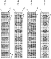
- FIGs. 2a-h show top views of 3D FP structure with recesses 7 of different sizes and shapes. Any suitable shapes and sizes can be used.
- FIGs. 2a-h are similar to Fig.1a and show the recesses filled by the lower electrode regions 3.
- FIGs. 3a and 3b shows different cross sections of the 3D FP structure FPS, however, different cross-scctional shapes can also be used.
- FIG.4a shows the top view of one variation of an embodiment of a 3D FP structure FPS in which the trenches 7 extend beyond the area of the device or chip covered by the upper electrode region 2 on a first side of the upper electrode region 2.
- Lower electrode regions 3 may extend into the trenches 7.
- Lower electrode regions 3 may fill all or a portion of the trenches 7. For example, if lower electrode regions 3 fill a portion of the trenches 7, the lower electrode regions may fill the portion of trenches 7 lying below the upper electrode region 2.
- the electrode structure may have a cross section as illustrated in FIG. 1b or FIG. 1c , for example.
- FIG.4b shows the top view of one exemplary variation of an embodiment of a 3D FP structure FPS in which the trenches 7 extend beyond the area of the device or chip covered by the upper electrode region 2 on a second side of the upper electrode region 2.
- Lower electrode regions 3 may extend into the trenches 7.
- Lower electrode regions 3 may fill all or a portion of the trenches 7. For example, if lower electrode regions 3 fill a portion of the trenches 7, the lower electrode regions may fill the portion of trenches 7 lying below the upper electrode region 2.
- the electrode structure 1d may have a cross section as illustrated in FIG. 1b or FIG. 1c , for example.
- FIG.4c shows the top view of one variation of an embodiment of a 3D FP structure 2 in which the trenches 7 extend beyond the area of the chip covered by the upper electrode region 2 on both a first side and a second side of the upper electrode region 2.
- Lower electrode regions 3 may extend into the trenches 7.
- Lower electrode regions 3 may fill all or a portion of the trenches 7. For example, if lower electrode regions 3 fill a portion of the trenches 7, the lower electrode regions may fill the portion of trenches 7 lying below the upper electrode region 2.
- the electrode structure may have a cross section as illustrated in FIG. 1b or FIG. 1c , for example.
- FIG. 5 shows one exemplary fabrication method of the 3D FP structure FPS in some embodiments, in which the semiconductor material or layer 4 ( FIG. 5(a) ) is firstly recessed ( FIG. 5(b) ), followed by formation of an optional insulation region 5 ( FIG. 5(c) ) and conductive electrode 2 and conductive electrode 3 ( FIG. 5(d) ).
- Any suitable recess technique can be used for making the recesses 7 such as dry etching, wet etching, etc.
- FIG. 6 shows another exemplary fabrication method of the 3D FP structure FPS, in which the semiconductor material or layer 4 is formed by selective growth ( FIG. 6(a) and (b) ), followed by formation of optional insulation region 5 ( FIG. 6(c) ) and conductive electrode 2 and conductive electrode 3 ( FIG. 6(d) ).
- Any suitable selective growth technique can be used for making the recesses 7 such as masked growth, catalyst, etc.
- FIG. 7 shows a top view of an example of a field effect transistor formed in or comprising a semiconductor material or layer 4 in which the 3D FP structure FPS is floating.
- the exemplary field effect transistor may be for example a HEMT (High Electron Mobility Transistor), MIS-HEMT (Metal-Insulator-Semiconductor-HEMT), MISFET (Metal-Insulator-Semiconductor Field Effect Transistor), JFET (Junction Field Effect Transistor) or a MESFET (Metal-Semiconductor Field Effect Transistor).
- HEMT High Electron Mobility Transistor
- MIS-HEMT Metal-Insulator-Semiconductor-HEMT
- MISFET Metal-Insulator-Semiconductor Field Effect Transistor
- JFET Joint Field Effect Transistor
- MESFET Metal-Semiconductor Field Effect Transistor
- the Field effect transistor includes a source region 11 and a drain region 12. Between source region 11 and drain region 12 is formed a gate region 1, which extends only a portion of the distance between the source region 11 and the drain region 12.
- the 3D FP region or structure FPS which extends only a portion of the distance between the gate region 11 and the drain region 12.
- the 3D FP structure FPS can be connected to the source 11, gate 1, drain 12, or even a few of them together.
- the number of 3D FP structures FPS can be one or larger than one.
- the 3D FP region is floating in the exemplary embodiment of FIG.7 and not connected or directly connected (in contact or direct contact with) to the source 11, gate 1 or the drain 12.
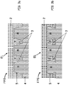
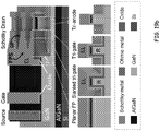
- FIGs. 8a to 8d show top views of 3D FP structures connected to the gate 1 with different extensions of the recesses 7.
- the conductive electrodes in gate 1 and 3D FP structures FPS can be of the same or different conductive materials.
- FIG. 8a shows a top view of a field effect transistor in which the 3D FP structure FPS is connected to the gate region 1 and the recesses 7 are only in the 3D FP structure.
- FIG. 8b shows a top view of a field effect transistor in which the 3D FP structure FPS is connected to the gate region 1 and the recesses 7 arc both in the 3D FP structure FPS and gate region 1.
- FIG. 8c shows a top view of a field effect transistor in which the 3D FP structure is connected to the gate region 1 and the recesses 7 extend from the 3D FP structure FPS into the gate region 1.
- FIG. 8d shows a top view of a field effect transistor in which the 3D FP structure is connected to the gate region 1 and the recesses 7 extend from the 3D FP structure FPS into the gate region 1 as well as into the semiconductor material or layer 4.
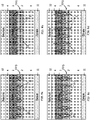
- FIGs. 9a to 9d show exemplary top views of 3D FP structures with different connections, sizes and shapes. Any possible connections, sizes and shapes can be used.
- FIG. 9a shows a top view of a field effect transistor with multiple 3D FP structures FPS, where one 3D FP structures FPS is connected to the gate 1.
- FIG. 9b shows a top view of a field effect transistor with multiple 3D FP structures FPS all connected to each other.
- FIG. 9c shows a top view of a field effect transistor with multiple 3D FP structures FPS, where the 3D FP structures FPS have recesses 7 and regions R of different lengths and sizes.
- FIG. 9d shows a top view of a field effect transistor multiple 3D FP structures FPS similar to those of Fig.9c and with all 3D FP structures connected to each other.
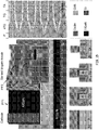
- FIG. 10a shows an example of a prototype device of a GaN transistor which has been fabricated.
- the AlGaN/GaN epitaxy in this exemplary structure consisted of 3.75- ⁇ m buffer, 0.3- ⁇ m un-doped GaN (u-GaN), 23.5-nm AlGaN barrier and 2-nm u-GaN cap layers.
- the device fabrication started with e-beam lithography to define the mesa and recesses, which were then etched by Cl 2 -based inductively coupled plasma and followed by ohmic metal deposition and rapid thermal annealing.
- the depth ( d1 ) of the recesses 7 formed in the semiconductor layers 4a and 4b was about 160 nm.
- the width w1 and length l1 for the recesses 7 formed in the semiconductor layers were 350 and 700 nm, respectively, with a period ( p ) of 750 nm.
- Al 2 O 3 was deposited by atomic layer deposition as a gate dielectric.
- the dimensions of the resulting depression DP are thus slightly less than the dimensions of the recess 7 in the semiconductor layers 4a and 4b.
- the gate was formed using Ni/Au, which was later used as the mask for removal of the Al 2 O 3 in access/ohmic regions.
- AlGaN/GaN transistors with similar dimensions but no recesses were taken as reference.
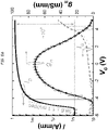
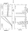
- FIGs. 11a and 11b show the on-state characteristics of the HEMT, indicating good performance.
- a breakdown voltage as high as 1350 V was measured at a drain leakage current of 1 ⁇ A/mm.
- the new device demonstrates the best performance and high breakdown voltage with a record high power FOM of 1.17 GW/cm 2 compared to the previous results in literature.
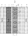
- FIG. 13 shows the schematic and FIGs. 14 and 15 show an actual exemplary prototype device of a fabricated GaN diode which includes a 3D FP structure FPS as described herein.
- FIG. 13 shows a top view schematic of the diode. As shown in FIG. 13 , the diode includes an anode region 13 and a cathode region 14 and the 3D FP structure FPS is connected to the anode.
- FIG. 14 shows a top view scanning electron microscope image of the diode. Fig.15 shows more details of the diode structure.
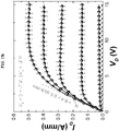
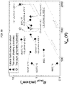
- FIG. 16 shows the forward and reverse characteristics of the SBDs with the 3D FP structure FPS as shown for example in FIGs. 13 and 14 and 15 , exhibiting small turn-on voltage and very small reverse leakage current.
- a breakdown voltage as high as 2500 V was measured for the 3D FP structure diode, with a small leakage current of 1 ⁇ A/mm up to 2000 V.
- the diode also exhibited much smaller leakage current than the results in the literature.
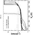
- FIG. 18 shows that the new device demonstrates high breakdown voltage and smaller leakage current compared to the any results in literature.
- FIGs. 19a-c show the schematic and prototype of an exemplary reverse-blocking GaN transistor fabricated with a Schottky drain 12, which was integrated with 3D FP structure with the 3D FP structure floating.
- FIG. 20a shows the excellent performance of the transistor as unidirectional transistor with small reverse leakage current.
- FIG. 19b shows the small turn-on voltage and good ideality factor (n) of the device, which are both independent of the gate voltage.
- Fig. 21 shows the high breakdown voltage of the transistor for both forward and reverse blocking, in which the breakdown was defined at 0.1 ⁇ A/mm with a grounded substrate.
- Fig. 22 shows the superior performance of the reverse-blocking transistor over any other GaN transistors with a Schottky drain.
- the present disclosure describes a field plate structure or 3D field plate structure to increase the breakdown voltage in semiconductor devices while guaranteeing ultra-low leakage current at reverse bias.
- the fabrication process of the 3D FP structure is much simpler than that of conventional field plates since it integrates the 3D FP fabrication process along with the device fabrication process.
- Exemplary embodiments concern a 3D FP structure to enhance voltage blocking of GaN lateral HEMTs and SBDs. These 3D FP structure significantly improved the breakdown voltage in transistors from 880 V to 1360 V at an off-state leakage current of 1 ⁇ A/mm, resulting in a new record high power FOM of 1.2 GW/cm 2 .
- the 3D FP structure largely improved the breakdown voltage of the SBDs to 2000 V at I R of 1 ⁇ A/mm and reduced the reverse leakage current (I R ) below 5 nA/mm with blocking voltage up to 700 V, respectively, rendering the highest breakdown voltage and a ultra-small leakage current among GaN lateral SBDs in the literature.
- the 3D FP structure was further implemented into the drain electrode of the transistor and led to reverse-blocking GaN transistor with record performance, which is significantly better other similar reports in the literature.
Landscapes
- Electrodes Of Semiconductors (AREA)
- Insulated Gate Type Field-Effect Transistor (AREA)
Claims (15)
- Dispositif semi-conducteur comportant :- une première électrode ;- une deuxième électrode ;- au moins un matériau ou couche semi-conducteur (4) entre la première et la deuxième électrode ;le dispositif semi-conducteur comportant en outre au moins une structure de plaque de champ (FPS) destinée à augmenter une tension de claquage du dispositif semi-conducteur, l'au moins une structure de plaque de champ (FPS) comprenant :- au moins deux encoches (7) dans l'au moins un matériau ou couche semi-conducteur (4), les au moins deux encoches (7) définissant une région semi-conductrice (R) entre elles, et- une troisième électrode (EL) en contact avec ou disposée sur la région semi-conductrice (R), la troisième électrode (EL) comportant un matériau conducteur,
la région semi-conductrice (R) comprenant une première paroi latérale (S1) et une deuxième paroi latérale (S2), le dispositif semi-conducteur étant un dispositif semi-conducteur latéral et étant caractérisé en ce que la première paroi latérale (S1) et la deuxième paroi latérale (S2) :s'étendent pour définir une forme de sablier en s'étendant simultanément de façon linéaire et convergente et ensuite de façon linéaire et divergente l'une par rapport à l'autre le long d'une direction allant de la première électrode à la deuxième électrode ; ouconsistent en (i) une première partie dans laquelle la première paroi latérale (S1) et la deuxième paroi latérale (S2) s'étendent de façon sensiblement parallèle l'une à l'autre le long d'une direction allant de la première électrode à la deuxième électrode et (ii) une deuxième partie dans laquelle la première paroi latérale (S1) et la deuxième paroi latérale (S2) s'étendent de façon divergente l'une par rapport à l'autre le long d'une direction allant de la première électrode à la deuxième électrode, oucomportent (i) une première partie dans laquelle la première paroi latérale (S1) et la deuxième paroi latérale (S2) s'étendent de façon sensiblement parallèle l'une à l'autre le long d'une direction allant de la première électrode à la deuxième électrode et (ii) une deuxième partie dans laquelle la première paroi latérale (S1) et la deuxième paroi latérale (S2) s'étendent d'une manière incurvée le long d'une direction allant de la première électrode à la deuxième électrode ; oula première paroi latérale (S1) s'étend sur une distance plus courte que la deuxième paroi latérale (S2) le long d'une direction allant de la première électrode à la deuxième électrode, et la première paroi latérale (S1) et la deuxième paroi latérale (S2) comportent (i) une première partie dans laquelle la première paroi latérale (S1) et la deuxième paroi latérale (S2) s'étendent de façon sensiblement parallèle l'une à l'autre le long d'une direction allant de la première électrode à la deuxième électrode et (ii) une deuxième partie dans laquelle la première paroi latérale (S1) et la deuxième paroi latérale (S2) s'étendent de façon convergente ou divergente l'une par rapport à l'autre le long d'une direction allant de la première électrode à la deuxième électrode. - Dispositif selon la revendication 1, dans lequel les au moins deux encoches (7) s'étendent partiellement à travers l'au moins un matériau ou couche semi-conducteur (4), ou une des au moins deux encoches (7) s'étend partiellement à travers l'au moins un matériau ou couche semi-conducteur (4).
- Dispositif selon l'une quelconque des revendications précédentes, dans lequel les au moins deux encoches (7) s'étendent entièrement à travers l'au moins un matériau ou couche semi-conducteur (4), ou une des au moins deux encoches (7) s'étend entièrement à travers l'au moins un matériau ou couche semi-conducteur (4).
- Dispositif selon l'une quelconque des revendications précédentes, dans lequel la troisième électrode (EL) recouvre partiellement ou recouvre entièrement la région semi-conductrice (R).
- Dispositif selon l'une quelconque des revendications précédentes, dans lequel la région semi-conductrice (R) comporte une surface supérieure (UL), et la troisième électrode (EL) recouvre partiellement ou recouvre entièrement au moins une paroi latérale (S1, S2) et/ou la surface supérieure (UL).
- Dispositif selon la revendication précédente, dans lequel la surface supérieure (UL) s'étend entre les première (S1) et deuxième (S2) parois latérales, et la troisième électrode (EL) s'étend le long de (i) la première paroi latérale (S1), la deuxième paroi latérale (S2) et la surface supérieure (UL), (ii) la première paroi latérale (S1) et la deuxième paroi latérale (S2), (iii) la première (S1) ou deuxième (S2) paroi latérale et la surface supérieure (UL), ou (iv) seulement la surface supérieure (UL).
- Dispositif selon l'une quelconque des revendications précédentes, dans lequel l'encoche (7) comporte un fond (F), et la troisième électrode (EL) s'étend pour recouvrir partiellement ou entièrement ledit fond (F) d'au moins une encoche (7) ou de chaque encoche (7).
- Dispositif selon l'une quelconque des revendications précédentes, dans lequel la troisième électrode (EL) s'étend pour remplir partiellement ou complètement au moins une encoche (7) ou chaque encoche (7) dans l'au moins un matériau ou couche semi-conducteur (4).
- Dispositif selon l'une quelconque des revendications précédentes, dans lequel la troisième électrode (EL) s'étend pour remplir partiellement au moins une encoche (7) ou chaque encoche (7) pour définir une cuvette (DP) dans l'au moins une encoche (7) ou chaque encoche (7).
- Dispositif selon l'une quelconque des revendications précédentes, dans lequel l'au moins un matériau ou couche semi-conducteur (4) est une couche plane comprenant au moins une partie plane non encastrée (PP1) et au moins une partie plane encastrée (PP2) comportant la structure de plaque de champ (FPS).
- Dispositif selon l'une quelconque des revendications précédentes, dans lequel la troisième électrode (EL) remplit les au moins deux encoches (7) et recouvre la région semi-conductrice (R) et recouvre au moins partiellement l'au moins un matériau ou couche semi-conducteur (4).
- Dispositif selon l'une quelconque des revendications précédentes, comportant en outre une région isolante (5) entre la région semi-conductrice (R) et la troisième électrode (EL).
- Dispositif selon une quelconque revendication précédente, dans lequel la troisième électrode (EL) de l'au moins une structure de plaque de champ (FPS) est directement en contact avec la première électrode ou la deuxième électrode.
- Dispositif selon l'une quelconque des revendications précédentes, comportant en outre une électrode de grille (1), et dans lequel la troisième électrode (EL) de l'au moins une structure de plaque de champ (FPS) est directement en contact avec l'électrode de grille (1).
- Dispositif selon la revendication précédente, dans lequel l'électrode de grille (1) s'étend à l'intérieur d'au moins une encoche de la structure de plaque de champ (FPS).
Applications Claiming Priority (2)
| Application Number | Priority Date | Filing Date | Title |
|---|---|---|---|
| US201662400643P | 2016-09-28 | 2016-09-28 | |
| PCT/IB2017/055961 WO2018060918A1 (fr) | 2016-09-28 | 2017-09-28 | Dispositif à semi-conducteur comprenant une plaque de champ tridimensionnelle |
Publications (2)
| Publication Number | Publication Date |
|---|---|
| EP3520142A1 EP3520142A1 (fr) | 2019-08-07 |
| EP3520142B1 true EP3520142B1 (fr) | 2022-04-20 |
Family
ID=60202277
Family Applications (1)
| Application Number | Title | Priority Date | Filing Date |
|---|---|---|---|
| EP17793728.1A Active EP3520142B1 (fr) | 2016-09-28 | 2017-09-28 | Dispositif à semi-conducteur comprenant une plaque de champ tridimensionnelle |
Country Status (3)
| Country | Link |
|---|---|
| US (1) | US11476357B2 (fr) |
| EP (1) | EP3520142B1 (fr) |
| WO (1) | WO2018060918A1 (fr) |
Families Citing this family (7)
| Publication number | Priority date | Publication date | Assignee | Title |
|---|---|---|---|---|
| US11894468B2 (en) * | 2018-11-06 | 2024-02-06 | Cornell University | High voltage gallium oxide (Ga2O3) trench MOS barrier schottky and methods of fabricating same |
| CN111757317B (zh) * | 2019-03-28 | 2021-12-28 | 上海华为技术有限公司 | 一种请求处理方法、相关装置及系统 |
| DE112021003124T5 (de) | 2020-06-04 | 2023-03-16 | Mitsubishi Electric Corporation | Halbleitereinheit |
| US11967619B2 (en) | 2020-09-16 | 2024-04-23 | Teledyne Scientific & Imaging, Llc | Laterally-gated transistors and lateral Schottky diodes with integrated lateral field plate structures |
| US12266721B2 (en) * | 2020-10-27 | 2025-04-01 | Wolfspeed, Inc. | Field effect transistor with multiple stepped field plate |
| US11923463B2 (en) | 2021-04-29 | 2024-03-05 | Virginia Tech Intellectual Properties, Inc. | Power Schottky barrier diodes with high breakdown voltage and low leakage current |
| KR102920262B1 (ko) * | 2022-10-07 | 2026-01-29 | 주식회사 디비하이텍 | 전력 반도체 소자 및 제조방법 |
Citations (2)
| Publication number | Priority date | Publication date | Assignee | Title |
|---|---|---|---|---|
| EP1073123A2 (fr) * | 1999-07-29 | 2001-01-31 | Kabushiki Kaisha Toshiba | Dispositif semiconducteur ayant une haute tenue en tension |
| US20110169103A1 (en) * | 2010-01-12 | 2011-07-14 | Maxpower Semiconductor Inc. | Devices, components and methods combining trench field plates with immobile electrostatic charge |
Family Cites Families (8)
| Publication number | Priority date | Publication date | Assignee | Title |
|---|---|---|---|---|
| JP4602465B2 (ja) * | 2008-12-04 | 2010-12-22 | 株式会社東芝 | 半導体装置 |
| WO2013055915A2 (fr) * | 2011-10-11 | 2013-04-18 | Massachusetts Institute Of Technology | Dispositifs semi-conducteurs ayant une structure d'électrode en retrait |
| US9035355B2 (en) * | 2012-06-18 | 2015-05-19 | Infineon Technologies Austria Ag | Multi-channel HEMT |
| US9735243B2 (en) | 2013-11-18 | 2017-08-15 | Infineon Technologies Ag | Semiconductor device, integrated circuit and method of forming a semiconductor device |
| JP5902116B2 (ja) * | 2013-03-25 | 2016-04-13 | 株式会社東芝 | 半導体装置 |
| JP6299581B2 (ja) * | 2014-12-17 | 2018-03-28 | 三菱電機株式会社 | 半導体装置 |
| DE102016113393B4 (de) * | 2016-07-20 | 2024-11-21 | Infineon Technologies Ag | Halbleitervorrichtung, die ein transistor-array und ein abschlussgebiet enthält, halbleitervorrichtung mit einem leistungstransistor in einem halbleitersubstrat und verfahren zum herstellen solch einer halbleitervorrichtung |
| DE102018119512B8 (de) * | 2018-08-10 | 2024-05-23 | Infineon Technologies Austria Ag | Nadelzellengraben-MOSFET |
-
2017
- 2017-09-28 EP EP17793728.1A patent/EP3520142B1/fr active Active
- 2017-09-28 WO PCT/IB2017/055961 patent/WO2018060918A1/fr not_active Ceased
- 2017-09-28 US US16/337,668 patent/US11476357B2/en active Active
Patent Citations (2)
| Publication number | Priority date | Publication date | Assignee | Title |
|---|---|---|---|---|
| EP1073123A2 (fr) * | 1999-07-29 | 2001-01-31 | Kabushiki Kaisha Toshiba | Dispositif semiconducteur ayant une haute tenue en tension |
| US20110169103A1 (en) * | 2010-01-12 | 2011-07-14 | Maxpower Semiconductor Inc. | Devices, components and methods combining trench field plates with immobile electrostatic charge |
Also Published As
| Publication number | Publication date |
|---|---|
| WO2018060918A1 (fr) | 2018-04-05 |
| US11476357B2 (en) | 2022-10-18 |
| EP3520142A1 (fr) | 2019-08-07 |
| US20190229208A1 (en) | 2019-07-25 |
Similar Documents
| Publication | Publication Date | Title |
|---|---|---|
| EP3520142B1 (fr) | Dispositif à semi-conducteur comprenant une plaque de champ tridimensionnelle | |
| US9041003B2 (en) | Semiconductor devices having a recessed electrode structure | |
| Ma et al. | Multi-channel tri-gate GaN power Schottky diodes with low ON-resistance | |
| JP4041075B2 (ja) | 半導体装置 | |
| EP3539159B1 (fr) | Dispositifs à semiconducteurs à canaux multiples et électrodes tridimensionnelles | |
| CN113690311B (zh) | 一种集成续流二极管的GaN HEMT器件 | |
| US10256314B2 (en) | Semiconductor device | |
| CN114747018A (zh) | 具有改进的漏极接近区域的iii族氮化物晶体管 | |
| Treu et al. | The role of silicon, silicon carbide and gallium nitride in power electronics | |
| Lei et al. | Reverse-blocking normally-OFF GaN double-channel MOS-HEMT with low reverse leakage current and low ON-state resistance | |
| CN108028273A (zh) | 半导体装置和制造半导体装置的方法 | |
| JP2007526633A (ja) | Iii族窒化膜双方向スイッチ | |
| JP2006086354A (ja) | 窒化物系半導体装置 | |
| CN110010562A (zh) | 半导体器件 | |
| Wei et al. | Low turn-on voltage and high breakdown voltage β-Ga 2 O 3 diode with fin channel and ohmic contact anode | |
| Palacios et al. | GaN 2.0: Power FinFETs, complementary gate drivers and low-cost vertical devices | |
| Esteghamat et al. | 2.7 kV E-Mode Multichannel GaN-on-Si based on p-type NiO/SiO 2 Junction Tri-gate | |
| US12495570B2 (en) | Vertical field-effect transistor, method for producing a vertical field-effect transistor and component having vertical field-effect transistors | |
| CN113707727B (zh) | 一种具有倒梯形槽的垂直GaN二极管 | |
| CN113611742B (zh) | 一种集成肖特基管的GaN功率器件 | |
| CN104538447A (zh) | 一种GaN基隧穿FinFET器件及其制造方法 | |
| CN120322011B (zh) | 半导体器件及功率设备 | |
| KR101887535B1 (ko) | 고전자 이동도 트랜지스터 및 그 제조방법 |
Legal Events
| Date | Code | Title | Description |
|---|---|---|---|
| STAA | Information on the status of an ep patent application or granted ep patent |
Free format text: STATUS: UNKNOWN |
|
| STAA | Information on the status of an ep patent application or granted ep patent |
Free format text: STATUS: THE INTERNATIONAL PUBLICATION HAS BEEN MADE |
|
| PUAI | Public reference made under article 153(3) epc to a published international application that has entered the european phase |
Free format text: ORIGINAL CODE: 0009012 |
|
| STAA | Information on the status of an ep patent application or granted ep patent |
Free format text: STATUS: REQUEST FOR EXAMINATION WAS MADE |
|
| 17P | Request for examination filed |
Effective date: 20190425 |
|
| AK | Designated contracting states |
Kind code of ref document: A1 Designated state(s): AL AT BE BG CH CY CZ DE DK EE ES FI FR GB GR HR HU IE IS IT LI LT LU LV MC MK MT NL NO PL PT RO RS SE SI SK SM TR |
|
| AX | Request for extension of the european patent |
Extension state: BA ME |
|
| DAV | Request for validation of the european patent (deleted) | ||
| DAX | Request for extension of the european patent (deleted) | ||
| STAA | Information on the status of an ep patent application or granted ep patent |
Free format text: STATUS: EXAMINATION IS IN PROGRESS |
|
| 17Q | First examination report despatched |
Effective date: 20200406 |
|
| GRAP | Despatch of communication of intention to grant a patent |
Free format text: ORIGINAL CODE: EPIDOSNIGR1 |
|
| STAA | Information on the status of an ep patent application or granted ep patent |
Free format text: STATUS: GRANT OF PATENT IS INTENDED |
|
| INTG | Intention to grant announced |
Effective date: 20211103 |
|
| GRAS | Grant fee paid |
Free format text: ORIGINAL CODE: EPIDOSNIGR3 |
|
| GRAA | (expected) grant |
Free format text: ORIGINAL CODE: 0009210 |
|
| STAA | Information on the status of an ep patent application or granted ep patent |
Free format text: STATUS: THE PATENT HAS BEEN GRANTED |
|
| AK | Designated contracting states |
Kind code of ref document: B1 Designated state(s): AL AT BE BG CH CY CZ DE DK EE ES FI FR GB GR HR HU IE IS IT LI LT LU LV MC MK MT NL NO PL PT RO RS SE SI SK SM TR |
|
| REG | Reference to a national code |
Ref country code: GB Ref legal event code: FG4D |
|
| REG | Reference to a national code |
Ref country code: CH Ref legal event code: EP |
|
| REG | Reference to a national code |
Ref country code: IE Ref legal event code: FG4D |
|
| REG | Reference to a national code |
Ref country code: DE Ref legal event code: R096 Ref document number: 602017056299 Country of ref document: DE |
|
| REG | Reference to a national code |
Ref country code: AT Ref legal event code: REF Ref document number: 1485885 Country of ref document: AT Kind code of ref document: T Effective date: 20220515 |
|
| REG | Reference to a national code |
Ref country code: LT Ref legal event code: MG9D |
|
| REG | Reference to a national code |
Ref country code: NL Ref legal event code: MP Effective date: 20220420 |
|
| PG25 | Lapsed in a contracting state [announced via postgrant information from national office to epo] |
Ref country code: NL Free format text: LAPSE BECAUSE OF FAILURE TO SUBMIT A TRANSLATION OF THE DESCRIPTION OR TO PAY THE FEE WITHIN THE PRESCRIBED TIME-LIMIT Effective date: 20220420 |
|
| PG25 | Lapsed in a contracting state [announced via postgrant information from national office to epo] |
Ref country code: SE Free format text: LAPSE BECAUSE OF FAILURE TO SUBMIT A TRANSLATION OF THE DESCRIPTION OR TO PAY THE FEE WITHIN THE PRESCRIBED TIME-LIMIT Effective date: 20220420 Ref country code: PT Free format text: LAPSE BECAUSE OF FAILURE TO SUBMIT A TRANSLATION OF THE DESCRIPTION OR TO PAY THE FEE WITHIN THE PRESCRIBED TIME-LIMIT Effective date: 20220822 Ref country code: NO Free format text: LAPSE BECAUSE OF FAILURE TO SUBMIT A TRANSLATION OF THE DESCRIPTION OR TO PAY THE FEE WITHIN THE PRESCRIBED TIME-LIMIT Effective date: 20220720 Ref country code: LT Free format text: LAPSE BECAUSE OF FAILURE TO SUBMIT A TRANSLATION OF THE DESCRIPTION OR TO PAY THE FEE WITHIN THE PRESCRIBED TIME-LIMIT Effective date: 20220420 Ref country code: HR Free format text: LAPSE BECAUSE OF FAILURE TO SUBMIT A TRANSLATION OF THE DESCRIPTION OR TO PAY THE FEE WITHIN THE PRESCRIBED TIME-LIMIT Effective date: 20220420 Ref country code: GR Free format text: LAPSE BECAUSE OF FAILURE TO SUBMIT A TRANSLATION OF THE DESCRIPTION OR TO PAY THE FEE WITHIN THE PRESCRIBED TIME-LIMIT Effective date: 20220721 Ref country code: FI Free format text: LAPSE BECAUSE OF FAILURE TO SUBMIT A TRANSLATION OF THE DESCRIPTION OR TO PAY THE FEE WITHIN THE PRESCRIBED TIME-LIMIT Effective date: 20220420 Ref country code: ES Free format text: LAPSE BECAUSE OF FAILURE TO SUBMIT A TRANSLATION OF THE DESCRIPTION OR TO PAY THE FEE WITHIN THE PRESCRIBED TIME-LIMIT Effective date: 20220420 Ref country code: BG Free format text: LAPSE BECAUSE OF FAILURE TO SUBMIT A TRANSLATION OF THE DESCRIPTION OR TO PAY THE FEE WITHIN THE PRESCRIBED TIME-LIMIT Effective date: 20220720 |
|
| PG25 | Lapsed in a contracting state [announced via postgrant information from national office to epo] |
Ref country code: RS Free format text: LAPSE BECAUSE OF FAILURE TO SUBMIT A TRANSLATION OF THE DESCRIPTION OR TO PAY THE FEE WITHIN THE PRESCRIBED TIME-LIMIT Effective date: 20220420 Ref country code: PL Free format text: LAPSE BECAUSE OF FAILURE TO SUBMIT A TRANSLATION OF THE DESCRIPTION OR TO PAY THE FEE WITHIN THE PRESCRIBED TIME-LIMIT Effective date: 20220420 Ref country code: LV Free format text: LAPSE BECAUSE OF FAILURE TO SUBMIT A TRANSLATION OF THE DESCRIPTION OR TO PAY THE FEE WITHIN THE PRESCRIBED TIME-LIMIT Effective date: 20220420 Ref country code: IS Free format text: LAPSE BECAUSE OF FAILURE TO SUBMIT A TRANSLATION OF THE DESCRIPTION OR TO PAY THE FEE WITHIN THE PRESCRIBED TIME-LIMIT Effective date: 20220820 |
|
| REG | Reference to a national code |
Ref country code: DE Ref legal event code: R097 Ref document number: 602017056299 Country of ref document: DE |
|
| PG25 | Lapsed in a contracting state [announced via postgrant information from national office to epo] |
Ref country code: SM Free format text: LAPSE BECAUSE OF FAILURE TO SUBMIT A TRANSLATION OF THE DESCRIPTION OR TO PAY THE FEE WITHIN THE PRESCRIBED TIME-LIMIT Effective date: 20220420 Ref country code: SK Free format text: LAPSE BECAUSE OF FAILURE TO SUBMIT A TRANSLATION OF THE DESCRIPTION OR TO PAY THE FEE WITHIN THE PRESCRIBED TIME-LIMIT Effective date: 20220420 Ref country code: RO Free format text: LAPSE BECAUSE OF FAILURE TO SUBMIT A TRANSLATION OF THE DESCRIPTION OR TO PAY THE FEE WITHIN THE PRESCRIBED TIME-LIMIT Effective date: 20220420 Ref country code: EE Free format text: LAPSE BECAUSE OF FAILURE TO SUBMIT A TRANSLATION OF THE DESCRIPTION OR TO PAY THE FEE WITHIN THE PRESCRIBED TIME-LIMIT Effective date: 20220420 Ref country code: DK Free format text: LAPSE BECAUSE OF FAILURE TO SUBMIT A TRANSLATION OF THE DESCRIPTION OR TO PAY THE FEE WITHIN THE PRESCRIBED TIME-LIMIT Effective date: 20220420 Ref country code: CZ Free format text: LAPSE BECAUSE OF FAILURE TO SUBMIT A TRANSLATION OF THE DESCRIPTION OR TO PAY THE FEE WITHIN THE PRESCRIBED TIME-LIMIT Effective date: 20220420 |
|
| PLBE | No opposition filed within time limit |
Free format text: ORIGINAL CODE: 0009261 |
|
| STAA | Information on the status of an ep patent application or granted ep patent |
Free format text: STATUS: NO OPPOSITION FILED WITHIN TIME LIMIT |
|
| 26N | No opposition filed |
Effective date: 20230123 |
|
| PG25 | Lapsed in a contracting state [announced via postgrant information from national office to epo] |
Ref country code: AL Free format text: LAPSE BECAUSE OF FAILURE TO SUBMIT A TRANSLATION OF THE DESCRIPTION OR TO PAY THE FEE WITHIN THE PRESCRIBED TIME-LIMIT Effective date: 20220420 |
|
| PG25 | Lapsed in a contracting state [announced via postgrant information from national office to epo] |
Ref country code: MC Free format text: LAPSE BECAUSE OF FAILURE TO SUBMIT A TRANSLATION OF THE DESCRIPTION OR TO PAY THE FEE WITHIN THE PRESCRIBED TIME-LIMIT Effective date: 20220420 |
|
| REG | Reference to a national code |
Ref country code: CH Ref legal event code: PL |
|
| REG | Reference to a national code |
Ref country code: BE Ref legal event code: MM Effective date: 20220930 |
|
| PG25 | Lapsed in a contracting state [announced via postgrant information from national office to epo] |
Ref country code: SI Free format text: LAPSE BECAUSE OF FAILURE TO SUBMIT A TRANSLATION OF THE DESCRIPTION OR TO PAY THE FEE WITHIN THE PRESCRIBED TIME-LIMIT Effective date: 20220420 |
|
| PG25 | Lapsed in a contracting state [announced via postgrant information from national office to epo] |
Ref country code: LU Free format text: LAPSE BECAUSE OF NON-PAYMENT OF DUE FEES Effective date: 20220928 |
|
| PG25 | Lapsed in a contracting state [announced via postgrant information from national office to epo] |
Ref country code: LI Free format text: LAPSE BECAUSE OF NON-PAYMENT OF DUE FEES Effective date: 20220930 Ref country code: IE Free format text: LAPSE BECAUSE OF NON-PAYMENT OF DUE FEES Effective date: 20220928 Ref country code: CH Free format text: LAPSE BECAUSE OF NON-PAYMENT OF DUE FEES Effective date: 20220930 |
|
| PG25 | Lapsed in a contracting state [announced via postgrant information from national office to epo] |
Ref country code: BE Free format text: LAPSE BECAUSE OF NON-PAYMENT OF DUE FEES Effective date: 20220930 |
|
| REG | Reference to a national code |
Ref country code: AT Ref legal event code: UEP Ref document number: 1485885 Country of ref document: AT Kind code of ref document: T Effective date: 20220420 |
|
| PG25 | Lapsed in a contracting state [announced via postgrant information from national office to epo] |
Ref country code: IT Free format text: LAPSE BECAUSE OF FAILURE TO SUBMIT A TRANSLATION OF THE DESCRIPTION OR TO PAY THE FEE WITHIN THE PRESCRIBED TIME-LIMIT Effective date: 20220420 |
|
| PG25 | Lapsed in a contracting state [announced via postgrant information from national office to epo] |
Ref country code: HU Free format text: LAPSE BECAUSE OF FAILURE TO SUBMIT A TRANSLATION OF THE DESCRIPTION OR TO PAY THE FEE WITHIN THE PRESCRIBED TIME-LIMIT; INVALID AB INITIO Effective date: 20170928 |
|
| PG25 | Lapsed in a contracting state [announced via postgrant information from national office to epo] |
Ref country code: CY Free format text: LAPSE BECAUSE OF FAILURE TO SUBMIT A TRANSLATION OF THE DESCRIPTION OR TO PAY THE FEE WITHIN THE PRESCRIBED TIME-LIMIT Effective date: 20220420 |
|
| PG25 | Lapsed in a contracting state [announced via postgrant information from national office to epo] |
Ref country code: MK Free format text: LAPSE BECAUSE OF FAILURE TO SUBMIT A TRANSLATION OF THE DESCRIPTION OR TO PAY THE FEE WITHIN THE PRESCRIBED TIME-LIMIT Effective date: 20220420 |
|
| PG25 | Lapsed in a contracting state [announced via postgrant information from national office to epo] |
Ref country code: MT Free format text: LAPSE BECAUSE OF FAILURE TO SUBMIT A TRANSLATION OF THE DESCRIPTION OR TO PAY THE FEE WITHIN THE PRESCRIBED TIME-LIMIT Effective date: 20220420 |
|
| PG25 | Lapsed in a contracting state [announced via postgrant information from national office to epo] |
Ref country code: BG Free format text: LAPSE BECAUSE OF FAILURE TO SUBMIT A TRANSLATION OF THE DESCRIPTION OR TO PAY THE FEE WITHIN THE PRESCRIBED TIME-LIMIT Effective date: 20220420 |
|
| REG | Reference to a national code |
Ref country code: DE Ref legal event code: R079 Ref document number: 602017056299 Country of ref document: DE Free format text: PREVIOUS MAIN CLASS: H01L0029400000 Ipc: H10D0064000000 |
|
| PG25 | Lapsed in a contracting state [announced via postgrant information from national office to epo] |
Ref country code: BG Free format text: LAPSE BECAUSE OF FAILURE TO SUBMIT A TRANSLATION OF THE DESCRIPTION OR TO PAY THE FEE WITHIN THE PRESCRIBED TIME-LIMIT Effective date: 20220420 |
|
| PGFP | Annual fee paid to national office [announced via postgrant information from national office to epo] |
Ref country code: DE Payment date: 20250919 Year of fee payment: 9 |
|
| PGFP | Annual fee paid to national office [announced via postgrant information from national office to epo] |
Ref country code: GB Payment date: 20250919 Year of fee payment: 9 |
|
| PGFP | Annual fee paid to national office [announced via postgrant information from national office to epo] |
Ref country code: FR Payment date: 20250922 Year of fee payment: 9 Ref country code: AT Payment date: 20250919 Year of fee payment: 9 |
|
| PG25 | Lapsed in a contracting state [announced via postgrant information from national office to epo] |
Ref country code: TR Free format text: LAPSE BECAUSE OF FAILURE TO SUBMIT A TRANSLATION OF THE DESCRIPTION OR TO PAY THE FEE WITHIN THE PRESCRIBED TIME-LIMIT Effective date: 20220420 |