EP3520170B1 - Breitbandiges mimo-antennensystem für elektronische vorrichtung - Google Patents
Breitbandiges mimo-antennensystem für elektronische vorrichtung Download PDFInfo
- Publication number
- EP3520170B1 EP3520170B1 EP18788042.2A EP18788042A EP3520170B1 EP 3520170 B1 EP3520170 B1 EP 3520170B1 EP 18788042 A EP18788042 A EP 18788042A EP 3520170 B1 EP3520170 B1 EP 3520170B1
- Authority
- EP
- European Patent Office
- Prior art keywords
- antennas
- antenna
- rim
- ground
- electronic device
- Prior art date
- Legal status (The legal status is an assumption and is not a legal conclusion. Google has not performed a legal analysis and makes no representation as to the accuracy of the status listed.)
- Active
Links
Images


Classifications
-
- H—ELECTRICITY
- H01—ELECTRIC ELEMENTS
- H01Q—ANTENNAS, i.e. RADIO AERIALS
- H01Q1/00—Details of, or arrangements associated with, antennas
- H01Q1/12—Supports; Mounting means
- H01Q1/22—Supports; Mounting means by structural association with other equipment or articles
- H01Q1/24—Supports; Mounting means by structural association with other equipment or articles with receiving set
- H01Q1/241—Supports; Mounting means by structural association with other equipment or articles with receiving set used in mobile communications, e.g. GSM
- H01Q1/242—Supports; Mounting means by structural association with other equipment or articles with receiving set used in mobile communications, e.g. GSM specially adapted for hand-held use
- H01Q1/243—Supports; Mounting means by structural association with other equipment or articles with receiving set used in mobile communications, e.g. GSM specially adapted for hand-held use with built-in antennas
-
- H—ELECTRICITY
- H01—ELECTRIC ELEMENTS
- H01Q—ANTENNAS, i.e. RADIO AERIALS
- H01Q1/00—Details of, or arrangements associated with, antennas
- H01Q1/48—Earthing means; Earth screens; Counterpoises
-
- H—ELECTRICITY
- H01—ELECTRIC ELEMENTS
- H01Q—ANTENNAS, i.e. RADIO AERIALS
- H01Q21/00—Antenna arrays or systems
- H01Q21/0006—Particular feeding systems
- H01Q21/0025—Modular arrays
-
- H—ELECTRICITY
- H01—ELECTRIC ELEMENTS
- H01Q—ANTENNAS, i.e. RADIO AERIALS
- H01Q21/00—Antenna arrays or systems
- H01Q21/28—Combinations of substantially independent non-interacting antenna units or systems
-
- H—ELECTRICITY
- H01—ELECTRIC ELEMENTS
- H01Q—ANTENNAS, i.e. RADIO AERIALS
- H01Q5/00—Arrangements for simultaneous operation of antennas on two or more different wavebands, e.g. dual-band or multi-band arrangements
- H01Q5/30—Arrangements for providing operation on different wavebands
-
- H—ELECTRICITY
- H01—ELECTRIC ELEMENTS
- H01Q—ANTENNAS, i.e. RADIO AERIALS
- H01Q9/00—Electrically-short antennas having dimensions not more than twice the operating wavelength and consisting of conductive active radiating elements
- H01Q9/04—Resonant antennas
- H01Q9/0407—Substantially flat resonant element parallel to ground plane, e.g. patch antenna
- H01Q9/0421—Substantially flat resonant element parallel to ground plane, e.g. patch antenna with a shorting wall or a shorting pin at one end of the element
-
- H—ELECTRICITY
- H01—ELECTRIC ELEMENTS
- H01Q—ANTENNAS, i.e. RADIO AERIALS
- H01Q21/00—Antenna arrays or systems
- H01Q21/30—Combinations of separate antenna units operating in different wavebands and connected to a common feeder system
Definitions
- the present disclosure relates to antennas, and in particular, to a broadband antenna and an arrangement of an antenna system in an electronic device.
- the antennas may be printed on a Printed Circuit Board (PCB) of the device.
- PCB Printed Circuit Board
- the layout of the PCB may need to be substantially changed or rearranged in order to print additional antennas on the ground plane of the PCB.
- the rim includes first and second side rim portions projecting from opposite sides of the back enclosure element.
- the first row of antennas is located in the first side rim portion.
- the MIMO antenna array includes a second row of antennas, and the second row of antennas is secured to the housing and located in the second side rim portion.
- the first row of antennas and the second row of antennas each include at least four antennas.
- the resonant frequency of the antennas is between 3 GHz and 6 GHz.
- the resonant frequency of the antennas is substantially 3.5GHz and the antennas are configured to receive or transmit RF signals within a frequency range of 3 GHz and 6 GHz.
- the first and second side rim portions are formed from metal, the antennas each being insert molded into the rim and having an outer surface forming part of an outer surface of the rim.
- the rim includes a top rim portion and a bottom rim portion that extend between the first and second side rim portions at a top and bottom of the housing respectively, the electronic device further including at least one further antenna located in one of the top rim portion and the bottom rim portion, the at least one further antenna having a different resonant frequency than the resonant frequency of the antennas of the MIMO antenna array.
- each of the antennas includes a resonating body secured to the rim, and a feed pad and a ground pad projecting from the resonating body into an inner region of the housing, the resonating body arranged substantially perpendicular with the feed pad and the ground pad.
- the RF communications circuit includes: an RF transceiver circuit comprising at least one integrated circuit component mounted on a printed circuit board (PCB); a plurality of signal paths extending through the PCB from the RF transceiver circuit to a plurality of electrical signal path connectors, each of the signal path connectors being in electrical contact with the feed pad of a respective one of the antennas; and a plurality of ground paths extending through the PCB from a common ground to a plurality of electrical ground path connectors, each of the ground path connectors being in electrical contact with the ground pad of a respective one of the antennas.
- PCB printed circuit board
- each of the signal path connectors and ground path connectors are spring biased to maintain pressure contact with the feed pads and ground pads, respectively.
- the resonating body and feed and ground pads of each of the antennas are configured to match an output impedance of the RF transceiver circuit without any intervening impedance matching circuitry.
- an electronic device that includes a housing enclosing a radio frequency (RF) communications circuit; and at least one antenna secured to the housing.
- the at least one antenna includes a resonating body with a feed pad and a ground pad extending from the resonating body.
- the feed pad is connected to the RF communications circuit.
- a ground pad is connected to a common ground as the RF communications circuit.
- the resonating body of the antenna having a length of 1 ⁇ 4 wavelength of a resonant frequency of the antenna, wherein the feed pad and the ground pad are positioned on the resonating body to provide an antenna impedance that matches an output impedance of the RF communications circuit, the resonating body arranged substantially perpendicular with the feed pad and the ground pad, wherein the housing comprises a back enclosure element and a forward projecting rim about a perimeter of the back enclosure element, the resonating body of the antenna being located on the rim, and wherein the RF communications circuitincludes: an RF transceiver circuit comprising at least one integrated circuit component mounted on a printed circuit board (PCB); at least one signal path extending through the PCB from the RF transceiver circuit to at least one electrical signal path connector, the signal path connector being a first spring loaded pressure contact connector and in electrical contact with the feed pad of the antenna; and at least one ground path extending through the PCB from a common ground to at least one electrical ground path connector
- the first row and the second row of antennas each include at least four of the antennas.
- the antenna impedance has a resistance in a range of 35 to 75ohm, and a reactance about 0 to +/- 20 Ohm, in the frequency range of 3-6 GHz.
- the output impedance of the RF communications circuit is 50ohm.
- a S11 of the antenna is substantially less or equal to -6dB.
- a method for installing a MIMO antenna array in an electronic device such as the one in claim 1.
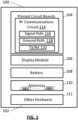
- FIG. 1 illustrates an example of an electronic device 100 according to the present disclosure.
- the electronic device 100 may be a mobile device that is enabled to receive and/or transmit radio frequency (RF) signals including for example, a tablet, a smart phone, a Personal Digital Assistant (PDA), or an Internet of Things (IOT) device, among other things.
- the electronic device 100 includes a housing 102 for enclosing hardware of the electronic device 100.
- Hardware of the electronic device may include at least one Printed Circuit Board (PCB) 104, a display module 106, a battery 108, one or more antenna devices 110 including an array of antennas 200(1) to 200(8) (referred to generically as antennas 200), and other hardware 112 including various circuits formed by electronic components populated on the PCB 104, sensors, speakers, or cameras.
- PCB Printed Circuit Board
- PCB 104 includes a plurality of layers including at least one signal layer and at least one ground layer.
- the signal layer includes a plurality of conductive traces that each form signal paths 116 between respective PCB pads.
- the ground layer of the PCB 104 provides a common ground reference in the PCB 104 for current returns of the electronic components and shielding, and includes a plurality of conductive traces that each form ground paths 118.
- Conductive vias are provided through the PCB 104 to extend the signal paths 116 and ground paths 118 to surface connection points (such as pads) on the PCB 104.
- Electronic components are populated on the PCB 104 to form circuits capable of performing desired functions.
- Electronic components may include, for example, integrated circuit (IC) chips, capacitors, resistors, inductors, diodes, transistors and other components.
- transceiver circuit 120 includes components to implement transmitter circuitry that modulates baseband signals to a carrier frequency and amplifies the resulting modulated RF signals. The amplified RF signals are then sent from the transceiver circuit 120 using signal path 116 and ground path 118 to the antennas 200 which then radiate the amplified RF signals into a wireless transmission medium.
- transceiver circuit 120 includes components to implement receiver circuitry that receives external carrier frequency modulated RF signals through signal path 116 and ground path 118 from the antennas 200.
- the transceiver circuit 120 may include a low noise amplifier (LNA) for amplifying the received signals and a demodulator for demodulating the received RF signals to baseband.
- LNA low noise amplifier
- RF transceiver circuit 120 may be replaced with a transmit-only circuitry and in some examples, RF transceiver circuit 120 may be replaced with a receiver-only circuitry.
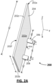
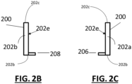
- FIGS 2A-2C illustrate an example broadband antenna 200 that is capable of transmitting RF signals received from a transmitter of the transceiver circuit 120 of the electronic device 100 and/or receiving external RF signals for further processing by a receiver of the transceiver circuit 120 of the electronic device 100.
- the antenna 200 comprises first and second terminals in the form of a feed pad 206, and a ground pad 208, and includes a resonating element in the form of a resonating body 204.
- the body 204, the feed pad 206 and the ground pad 208 may be made of metal, such as copper.
- the feed pad 206 and the ground pad 208 are electrically connected to the body 204.
- Each of the feed pad 206 and the ground pad 208 has a first end electrically connected to the body 204, for example, on the inner side 202e and close to the bottom edge 202d of the body 204.
- Each of the feed pad 206 and the ground pad 208 extends inwardly from inner surface 202e to a respective second distal end.
- Each of the feed pad 206 and the ground pad 208 may have a substantially rectangular shape.
- each of the feed pad 206 and the ground pad 208 may be a rectangular metal tab.
- the feed pad 206 is electrically connected to transceiver circuit 120 through the signal path 116 of RF communications circuit 114.
- the ground pad 208 is electrically connected to a common ground through the ground path 118 of the PCB 104.
- the feed pad 206 and the ground pad 208 are substantially perpendicular with the inner side 202e of the body 204.
- the inner side 202e of the body 204 is substantially in an XZ plane, and the feed pad 206 and the ground pad 208 are substantially in the XY plane.
- the feed pad 206 and the ground pad 208 extend inward from the inner side 201e at the bottom edge 202d of the body 204 and are located between the first side edge 202a and the second side edge 202b of the antenna body 204.
- the length of the antenna body 204 is substantially about 1 ⁇ 4 wavelength ( ⁇ ) of the resonant frequency of the antenna 200.
- the length of the antenna body 204 is d1
- the distance between the feed pad 206 and the ground pad 208 is d4
- the distance between the second side edge 202b and the ground pad 208 is d2
- the distance between the first side edge 202a and the feed pad 206 is d6
- the widths of the feed pad 206 and the ground pad 208 are d5 and d3, respectively.
- d1 d2+d3+d4+d5+d6.
- d2 and d6 are equal and d3 is equal to d5. In some embodiments, d4 is equal to the sum of d2 and d6.
- the antenna 200 is integrated into side edge or rim portions of device 100, and in such cases the height h of the antenna 200 is selected in accordance with the thickness of the device 100.
- the output impedance of the RF communications circuit 114 (which includes the transceiver circuit 120 and signal and ground paths 116,118) may be purely resistive (for example, 50 Ohm).
- the impedance Z of the antenna 200 is configured to "match" the output impedance of the RF communications circuit 114, without using any additional impedance matching circuit or impedance compensating circuit. Accordingly, in example embodiments, in the state of "impedance matching", the antenna 200 is configured to have an impedance that has negligible reactance and has a resistance that falls within a defined range of the output resistance of the RF communications circuit 114.
- the antenna 200 is configured such that the impedance Z of the antenna 200 has a resistance R about 35 to 75ohm, and a reactance X about 0 to +/- 20 Ohm, at the resonant frequency and within the frequency range.
- any power loss in signals exchanged between the antenna 200 and RF communications circuit 114 is within an acceptable threshold level at the resonant frequency and within the frequency range (bandwidth) of the antenna 200.
- the power loss in signals exchanged between the antenna 200 and RF communications circuit 114 is represented by a parameter S11, which indicates the power level reflected from the antenna 200.
- S11 is also known as the reflection coefficient gamma ⁇ or return loss.
- the width of each of the feed pad 206 (d5) and the ground pad 208 (d3) is 2mm.
- the antenna 200 has a high efficiency.
- an array of such antennas may have a total and radiation Rx efficiency of above 60% across most of the frequency range of 3GHz to 6GHz.
- the antenna 200 in this example also has a good impedance matching at the frequency range of 3GHz to 6 GHz.
- an array of such antennas has a scattering parameter S Rx-Rx substantially less than -10 dB in most of the frequency range from 3GHz to 6GHz.
- antenna 200 is a planar antenna having a structure that achieves impedance matching from 3 GHz to 6 GHz.
- the antenna 200 may, for example, be a Planar Inverted-F Antenna (PIFA), an Inverted-F Antenna, a monopole antenna, or a patch antenna.
- PIFA Planar Inverted-F Antenna
- Inverted-F Antenna a monopole antenna
- patch antenna a patch antenna.
- antenna 200 does not need an extra impedance matching circuit to achieve the "impedance matching" state in order for the antenna 200 to operate at the desired resonant frequency and bandwidth, for example, at resonant frequency 3.5 GHz and within the frequency range of 3 GHz-6GHz. Therefore, antenna 200 has a compact size and may be implemented in an electronic device 100, such as a 5G electronic device, without occupying excessive free space of the electronic device 100 or substantially changing or rearranging the existing layout of the PCB 104.
- the components of RF communications circuit 114 that connect the antenna 200 to the RF transceiver circuit 120 have negligible inductance, and the antenna 200 is configured to match the impedance of the RF transceiver circuit 120 without any intermediate RF tuning circuitry or impedance matching circuitry.
- the configuration of the resonating element body 204 and relative positioning of feed and ground pads 206 and 208 are selected to match the impedance of RF transceiver circuit 120 to meet the criteria stated above.
- a multiple-input and multiple-output (MIMO) antenna system may be used to increase the capacity of wireless channels.
- MIMO antenna array that includes a plurality of antennas 200 is integrated into the housing 102 of electronic device 100, and in this regard reference is now made to the example embodiment illustrated in Figures 3 and 4 .
- the housing 102 of electronic device 100 includes a rectangular, planar back enclosure element 302 that is surrounded by a forwardly projecting rim 301 that extends around the outer periphery of back enclosure element 302.
- the rim 301 and back enclosure element 302 define the back and sides of an internal region 303 that contains hardware of the device 100, including PCB 104.
- the electronic device 100 will typically also include a front enclosure element that is secured to the front of the rim 301 and covers the front of the internal region 303 to enclose the internal device hardware.
- the front enclosure element is omitted for clarity.
- the front enclosure element incorporates user interface elements such as a touch display screen.
- the rim 301 includes a top rim portion 304, a bottom rim portion 306 and two opposite side rim portions 308 and 310 that extend between the top and bottom rim portions.
- Electronic devices intended for handheld use typically have a rectangular prism configuration with a top and bottom of the device that correspond to the orientation that the device is most commonly held in during handheld use, and the terms "top”, “bottom”, “front” and “back” as used herein refer to the most common use orientation of a device as intended by the device manufacturer, while recognizing that some devices can be temporarily orientated to different orientations (for example from a portrait orientation to a landscape orientation).
- each of the top rim 304, the bottom rim 306, and the two opposite side rims 308 and 310 has an inner surface and an outer surface.
- the back enclosure element 302 and the rim 301 are formed from suitable material, such as metal, plastic, carbon-fiber materials or other composites, glass, or ceramics, and eight antennas 200 are secured to the rim 301 of housing 102 to form an 8x8 MIMO antenna system.
- the feed pads 206 and the ground pads 208 of the 8 antennas 200 are arranged inside the housing 102 for electrically connecting with signal and ground paths 116, 118 of PCB 104.
- the antennas 200 are each secured into respective openings in the side rim portions 308 and 310 using an insert molding process with an insulating dielectric material 312 (see antenna 200(4)) extending around a perimeter of the antenna feed and ground pads 206, 208 and antenna body 204 to insulate the antenna 200 from the rest of the metal of housing 102 and secure the antenna 200 in place.
- insulating material 312 could include a plastic strip.
- the antennas 200(1)-200(4) are evenly spaced apart in a row along side rim portion 308 and the antennas 200(5)-200(8) are evenly spaced apart in a row along opposite side rim portion 310.
- the antennas 200(1)-200(4) are symmetrical with respect to the antennas 200(5)-200(8).
- the inner side 202e of the metal antenna body 204 of each of the antennas 200(1)-200(8) forms part of the inner surface of the side rim portions 308 and 310
- the outer side 202f of the metal antenna body 204 of each of the antennas 200(1)-200(8) forms part of the outer surface of the side rim portions 308 and 310.
- the thickness of the body 204 of the antennas 200a-200h and the non-antenna portions of side rim portions 308 and 310 are substantially the same, however in some example embodiments they may be different.
- an RF transceiver circuit 120 is mounted on PCB 104.
- Signal paths 116 and ground paths 118 are provided in respective layers of the PCB 104 between the RF transceiver circuit 120 to provide signal and ground connections between each of the antennas 200 and the RF transceiver circuit 120.
- Figure 4 is a partial cross-sectional illustration of the device 100 of Figure 3 , showing the connection of feed pad 206 of an antenna 200 (for example antenna 200(7)) to transceiver circuit 120 through a signal path 116 of PCB 104.
- the body 204 of antenna 200 forms part of the rim 301 (side rim portion 310 in the case of antenna 200(7)) of housing 102, with the inner side 202e of the antenna 200 facing housing inner region 303, and the outer side 202f of the antenna 200 facing outwards.
- the feed pad 206 of antenna 200 extends inward from the antenna body 204 and is integrated into an upper surface of the metal bottom enclosure element 302 such that a surface of the feed pad 206 is exposed in housing inner region 303.
- dielectric insulating material 312 extends between the metal bottom enclosure 302 and the components of antenna 200 (including feed pad 206 and ground pad 208) to insulate the antenna components from the metal bottom enclosure element 302.
- signal path 116 extends through PCB 104 between a first conductive pad 402 located on one side of the PCB 104 and a second conductive pad 404 located on the opposite side of the PCB.
- a signal input/output pad of RF transceiver circuit 120 is electrically connected (for example through a wave soldering process) to the first conductive pad 402.
- a connector, such as a spring loaded pressure contact connector, 212 is connected (for example through a wave soldering process) to the second conductive pad 404.
- the spring loaded connector 212 is clamped between the PCB 104 and the antenna feed pad 206, biasing the connector 212 into electrical contact with feed pad 206, thus providing a RF signal path between the RF transceiver circuit 120 and the antenna 200.
- the ground pad 208 of antenna 200 is similarly electrically connected by a further spring loaded connector to a ground path 118 in PCB 104.
- the spring loaded connectors 212, PCB signal path 116 and ground path 118, RF transceiver circuit 120, and any interconnecting conductive elements such as PCB pads 402, 404 collectively provide RF communications circuit 114.
- the impedance of antenna 200 is matched as per the criteria described above to the impedance of the RF communications circuit 114.
- the impedance of the connectors 212, PCB paths 116 and 118 and any interconnecting conductive elements such as PCB pads 402, 404 is general negligible and can be ignored in impedance matching of the antenna 200 and the RF transceiver circuit 120.
- Different electrical connections can be used between the antenna 200 and the PCB 104 than the spring clip style connector 212 shown in Figure 4 .
- a spring loaded pogo-pin style connector could alternatively be used.
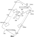
- Antennas 200(1)-200(4) arranged on the inner surface of side rim portion 308 are not shown because they are hidden in the perspective view of Figure 5 .
- the thickness of the body 204 of the metal antennas 200 (1)-200(8) and the side rim portions 308, 310 may be different or substantially the same.
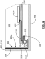
- the partial sectional view of Figure 6 illustrates the mounting an antenna 200 (for example antenna 200(7)) to the plastic side rim portion 310 of rim 301 in greater detail.
- the body 204 of antenna 200 is secured to the inner surface of rim portion 310, with the inner side 202e of the antenna 200 facing housing inner region 303, and the outer side 202f of the antenna 200 facing the rim portion 310, which is formed from a non-conductive RF-transparent material.
- the feed pad 206 of antenna 200 extends inward from the antenna body 204 along a non-conducting upper surface of the bottom enclosure element 302 such that a surface of the feed pad 206 is exposed in housing inner region 303.
- the antenna 200 may be integrally formed on the rim portion 310 and bottom enclosure element 302.
- antenna 200 can be integrated into flex PCB 312 that is secured to the rim portion 310 and bottom enclosure element 302.
- the number, location and relative spacing of antennas 200 within the housing 102 can be different than described above.
- one or more antennas 200 could be placed on the top rim portion 304, the bottom rim portion 306, the back enclosure element 302 and/or the front cover of the housing 102.
- the antennas can be asymmetrically placed in some examples.
- the number of antennas could be fewer than or greater than eight, including as few as one.
- 4 antennas 200 may securely attach to the housing 102 to form a 4X4 MIMO antenna system, including for example 2 antennas 200 secured to each of the side rim portions 308 and 310 of the housing 102 to form a 4X4 MIMO antenna system.
- the antennas 200 secured to the housing 102 are substantially identical to each other and have a resonant frequency with the frequency range of 3 GHz-6GHz.
- the antennas 200 secured to the housing 102 have different resonant frequencies with the frequency range of 3 GHz-6GHz.
- a plurality of antennas 200 securely attached to side rim 308 of housing 102 have a resonant frequency of 3.5 GHz
- a plurality of antennas 200 securely attached to side rim 310 of housing 102 have a resonant frequency of 4.8GHz.
- a plurality of antennas 200 securely attached to a side rim 308 or 310 of housing 102 have different resonant frequencies.
- some of the antennas 200 have a resonant frequency of 3.5 GHz and other antennas 200 have a resonant frequency of 4.8 GHz.
- antennas having different configurations and tuned for other frequency ranges are also secured to housing 102, including for example antennas for 3.5GHz, 4.8GHz and sub 2.6GHz legacy bands.
- antennas secured to the housing 102 have different resonant frequencies and different frequency ranges.
- MIMO antenna systems such as those shown in in Figures 3 and 5 have a low correlation between different pairs of antennas 200.
- the Rx-Rx Envelope Correlation Coefficient Pearson
- the Rx-Rx Envelope Correlation Coefficient are substantially below 0.1 on the bandwidth from 3 GHz to 6 GHz. Because of the low correlation between different pairs of antennas, each of the antennas can function independently from the others, and this in turn maximizes wireless channel capacity represented by each antenna 200.
- MIMO antenna systems in Figures 3 and 5 can have a high efficiency in some configurations. According to measurement results of an 8X8 MIMO antenna analyzer EMITE chamber, the MIMO antenna systems in Figures 3 and 5 have a total and radiation Rx efficiency above 60% in most the frequency range from 3GHz to 6GHz.
- the MIMO antenna systems in Figures 3 and 5 also have a good impedance matching with the output impedance of a signal circuit 214, such as a transmitting and/or receiving circuit, of the electronic device 100 at the frequency range of 3GHz to 6 GHz.
- a signal circuit 214 such as a transmitting and/or receiving circuit
- the MIMO antenna systems in Figures 3 and 5 have scattering parameters S Rx-Rx equal or substantially less than -6 dB from 3GHz to 6GHz.
Landscapes
- Engineering & Computer Science (AREA)
- Computer Networks & Wireless Communication (AREA)
- Support Of Aerials (AREA)
- Details Of Aerials (AREA)
Claims (13)
- Elektronische Vorrichtung (100), umfassend:ein Gehäuse (102), das eine Hochfrequenz-, HF-, Kommunikationsschaltung (114) umhüllt; undein Multiple-Input-Multiple-Output-, MIMO-, Antennenarray, der mit der HF-Kommunikationsschaltung (114) elektrisch verbunden ist, wobei der MIMO-Antennenarray eine erste Reihe von Antennen (200) einschließt, die an dem Gehäuse (102) befestigt sind,wobei das Gehäuse (102) ein rückseitiges Umhüllungselement (302) umfasst, das von einem nach vorne vorstehenden Rand (301) umgeben ist, wobei sich die erste Reihe von Antennen (200) in dem Rand (301) befindet,wobei jede der Antennen (200) einen Resonanzkörper (204), der an dem Rand (301) befestigt ist, und eine Speisefläche (206) und eine Massefläche (208) einschließt, die von dem Resonanzkörper (204) in eine innere Region des Gehäuses (102) vorstehen, wobei der Resonanzkörper (204) zu der Speisefläche (206) und der Massefläche (208) im Wesentlichen senkrecht angeordnet ist,wobei die HF-Kommunikationsschaltung (114) einschließt: eine HF-Sendeempfängerschaltung (120), umfassend mindestens eine integrierte Schaltungskomponente, die auf einer Leiterplatte, PCB, gelagert ist;eine Vielzahl von Signalpfaden (116), die sich durch die PCB von der HF-Sendeempfängerschaltung (120) zu einer Vielzahl von elektrischen Signalpfadverbindern erstreckt, wobei jeder der Signalpfadverbinder ein erster federnder Druckkontaktverbinder (212) und mit der Speisefläche (206) einer jeweiligen einen der Antennen (200) in elektrischem Kontakt ist; und eine Vielzahl von Massepfaden (118), die sich durch die PCB von einer gemeinsamen Masse zu einer Vielzahl von elektrischen Massepfadverbindern erstreckt, wobei jeder der Massepfadverbinder ein zweiter federnder Druckkontaktverbinder und mit der Massefläche (208) einer jeweiligen einen der Antennen (200) in elektrischem Kontakt ist.
- Elektronische Vorrichtung nach Anspruch 1, wobei der Rand einen ersten und einen zweiten seitlichen Randabschnitt (308, 310) einschließt, die von gegenüberliegenden Seiten des rückseitigen Umhüllungselements vorstehen, wobei sich die erste Reihe von Antennen in dem ersten seitlichen Randabschnitt (308) befindet, wobei der MIMO-Antennenarray eine zweite Reihe von Antennen einschließt, wobei die zweite Reihe von Antennen an dem Gehäuse befestigt ist und sich in dem zweiten seitlichen Randabschnitt (310) befindet.
- Elektronische Vorrichtung nach Anspruch 2, wobei die erste Reihe von Antennen und die zweite Reihe von Antennen jeweils mindestens vier Antennen einschließen; und/oder,
wobei die Resonanzfrequenz der Antennen zwischen 3 GHz und 6 GHz ist. - Elektronische Vorrichtung nach Anspruch 2, wobei die Resonanzfrequenz der Antennen im Wesentlichen 3,5 GHz ist und die Antennen konfiguriert sind, um HF-Signale innerhalb eines Frequenzbereichs von 3 GHz und 6 GHz zu empfangen oder zu senden.
- Elektronische Vorrichtung nach einem der Ansprüche 2 bis 4, wobei der erste und der zweite seitliche Randabschnitt aus Metall ausgebildet sind, wobei die Antennen jeweils in den Rand einsatzgegossen sind und eine äußere Oberfläche aufweisen, die einen Teil einer äußeren Oberfläche des Randes ausbildet.
- Elektronische Vorrichtung nach einem der Ansprüche 2 bis 4,wobei der erste und der zweite seitliche Randabschnitt aus Kunststoff ausgebildet sind, wobei die Antennen jeweils auf dem Rand unter Verwendung eines Laserdirektstrukturierungs-, LDS-, Prozesses ausgebildet werden; und/oder,wobei der erste und der zweite seitliche Randabschnitt aus Kunststoff ausgebildet sind, wobei die Antennen jeweils in eine flexible Leiterplatte, PCB, integriert sind, die an dem Rand befestigt ist.
- Elektronische Vorrichtung nach einem der Ansprüche 2 bis 6, wobei der Rand einen oberen Randabschnitt (304) und einen unteren Randabschnitt (306) einschließt, die sich zwischen dem ersten und dem zweiten seitlichen Randabschnitt an einer Oberseite beziehungsweise einer Unterseite des Gehäuses erstrecken, wobei die elektronische Vorrichtung ferner mindestens eine weitere Antenne einschließt, die sich in einem des oberen Randabschnitts und des unteren Randabschnitts befindet, wobei die mindestens eine weitere Antenne eine andere Resonanzfrequenz als die Resonanzfrequenz der Antennen des MIMO-Antennenarrays aufweist.
- Elektronische Vorrichtung nach einem der Ansprüche 2 bis 7, wobei der Resonanzkörper eine Länge von ¼ der Resonanzfrequenzwellenlänge aufweist.
- Elektronische Vorrichtung (100), umfassend:ein Gehäuse (102), das eine Hochfrequenz-, HF-, Kommunikationsschaltung (114) umhüllt; undmindestens eine Antenne (200), die an dem Gehäuse (102) befestigt ist, die mindestens eine Antenne umfassend einen Resonanzkörper (204) mit einer Speisefläche (206) und einer Massefläche (208), die sich von dem Resonanzkörper (204) erstrecken, wobei die Speisefläche (206) mit der HF-Kommunikationsschaltung (114) verbunden und die Massefläche (208) mit einer gemeinsamen Masse wie die HF-Kommunikationsschaltung (114) verbunden ist;wobei der Resonanzkörper (204) der Antenne (200) eine Länge von ¼ Wellenlänge einer Resonanzfrequenz der Antenne (200) aufweist, wobei die Speisefläche (206) und die Massefläche (208) konfiguriert sind, um auf dem Resonanzkörper (204) positioniert zu sein, um eine Antennenimpedanz bereitzustellen, die mit einer Ausgangsimpedanz der HF-Kommunikationsschaltung (114) übereinstimmt, wobei der Resonanzkörper (204) zu der Speisefläche (206) und der Massefläche (208) im Wesentlichen senkrecht angeordnet ist, wobei das Gehäuse (102) ein rückseitiges Umhüllungselement (302) und einen nach vorne vorstehenden Rand (301) um einen Umfang des rückseitigen Umhüllungselements (302) herum umfasst, wobei sich der Resonanzkörper (204) der Antenne (200) auf dem Rand (301) befindet,wobei die HF-Kommunikationsschaltung (114) einschließt: eine HF-Sendeempfängerschaltung (120), umfassend mindestens eine integrierte Schaltungskomponente, die auf einer Leiterplatte, PCB, gelagert ist;mindestens einen Signalpfad (116), der sich durch die PCB von der HF-Sendeempfängerschaltung (120) zu mindestens einem elektrischen Signalpfadverbinder erstreckt, wobei der Signalpfadverbinder ein erster federnder Druckkontaktverbinder (212) und mit der Speisefläche (206) der Antenne (200) in elektrischem Kontakt ist; und mindestens einen Massepfad (118), der sich durch die PCB von einer gemeinsamen Masse zu mindestens einem elektrischen Massepfadverbinder erstreckt, wobei der Massepfadverbinder ein zweiter federnder Druckkontaktverbinder und mit der Massefläche (208) der Antenne (200) in elektrischem Kontakt ist.
- Elektronische Vorrichtung nach Anspruch 9,
wobei der Rand einen oberen Randabschnitt (304), der sich an einer Oberseite der elektronischen Vorrichtung befindet, einen unteren Randabschnitt (306), und zwei gegenüberliegende seitliche Ränder (308, 310) einschließt, die sich zwischen dem oberen und dem unteren Rand erstrecken, wobei die elektronische Vorrichtung ein MIMO-Antennenarray umfasst, der eine erste Reihe der Antennen und eine zweite Reihe der Antennen einschließt, wobei sich die Resonanzkörper der ersten Reihe von Antennen auf einem der seitlichen Ränder befinden und sich die Resonanzkörper der zweiten Reihe von Antennen auf dem anderen der seitlichen Ränder befinden. - Elektronische Vorrichtung nach Anspruch 10, wobei die erste Reihe und die zweite Reihe von Antennen jeweils mindestens vier der Antennen einschließen.
- Elektronische Vorrichtung nach einem der Ansprüche 9 bis 11, wobei die Antennenimpedanz einen Widerstand in einem Bereich von 35 bis 75 Ohm und eine Reaktanz von etwa 0 bis +/- 20 Ohm in dem Frequenzbereich von 3-6 GHz aufweist und wobei die Ausgangsimpedanz der HF-Kommunikationsschaltung 50 Ohm ist; und/oder,
wobei ein S11 der Antenne im Wesentlichen kleiner oder gleich -6 dB ist. - Verfahren zum Installieren eines MIMO-Antennenarrays (200) in einer elektronischen Vorrichtung (100), die elektronische Vorrichtung (100) umfassend eine Hochfrequenz-, HF-, Kommunikationsschaltung (114), die innerhalb eines Gehäuses (102) zum Aufnehmen der Hardware aufgenommen wird, das Verfahren umfassend:Befestigen einer Reihe von Antennen (200), die jeweils eine gleiche Resonanzfrequenz aufweisen, an dem Gehäuse (102), wobei jede Antenne (200) eine Speisefläche (206) und eine Massefläche (208) aufweist, die sich von einem Resonanzkörper (204) in eine innere Region des Gehäuses (102) erstrecken, wobei der Resonanzkörper (204) zu der Speisefläche (206) und der Massefläche (208) im Wesentlichen senkrecht angeordnet ist; undVerbinden der Speiseflächen (206) mit Signalpfaden (116) der HF-Kommunikationsschaltung (114) und Verbinden der Masseflächen (208) mit einer gemeinsamen Masse, wobei das Gehäuse (102) ein rückseitiges Umhüllungselement (302) umfasst, das von dem nach vorne vorstehenden Rand (301) umgeben ist, wobei sich die Reihe von Antennen (200) in dem Rand (301) befindet,wobei die HF-Kommunikationsschaltung (114) einschließt: eine HF-Sendeempfängerschaltung (120), umfassend mindestens eine integrierte Schaltungskomponente, die auf einer Leiterplatte, PCB, gelagert ist;wobei sich die Signalpfade von der HF Sendeempfängerschaltung durch die PCB zu einer Vielzahl von elektrischen Signalpfadverbindern erstrecken, wobei jeder der Signalpfadverbinder ein erster federnder Druckkontaktverbinder (212) und mit der Speisefläche einer jeweiligen einen der Antennen in elektrischem Kontakt ist; und sich die Massepfade durch die PCB von der gemeinsamen Masse zu einer Vielzahl von elektrischen Massepfadverbindern erstrecken, wobei jeder der Massepfadverbinder ein zweiter federnder Druckkontaktverbinder und mit der Massefläche einer jeweiligen einen der Antennen in elektrischem Kontakt ist.
Applications Claiming Priority (2)
| Application Number | Priority Date | Filing Date | Title |
|---|---|---|---|
| US15/494,048 US20180309189A1 (en) | 2017-04-21 | 2017-04-21 | Broadband mimo antenna system for electronic device |
| PCT/CN2018/083624 WO2018192538A1 (en) | 2017-04-21 | 2018-04-19 | Broadband mimo antenna system for electronic device |
Publications (3)
| Publication Number | Publication Date |
|---|---|
| EP3520170A1 EP3520170A1 (de) | 2019-08-07 |
| EP3520170A4 EP3520170A4 (de) | 2019-10-30 |
| EP3520170B1 true EP3520170B1 (de) | 2023-05-31 |
Family
ID=63852411
Family Applications (1)
| Application Number | Title | Priority Date | Filing Date |
|---|---|---|---|
| EP18788042.2A Active EP3520170B1 (de) | 2017-04-21 | 2018-04-19 | Breitbandiges mimo-antennensystem für elektronische vorrichtung |
Country Status (4)
| Country | Link |
|---|---|
| US (1) | US20180309189A1 (de) |
| EP (1) | EP3520170B1 (de) |
| CN (1) | CN110235308A (de) |
| WO (1) | WO2018192538A1 (de) |
Families Citing this family (11)
| Publication number | Priority date | Publication date | Assignee | Title |
|---|---|---|---|---|
| KR102364470B1 (ko) * | 2017-08-23 | 2022-02-18 | 삼성전자주식회사 | 안테나를 포함하는 전자 장치 |
| KR102424681B1 (ko) * | 2017-11-27 | 2022-07-25 | 삼성전자주식회사 | 통신 장치 배치 구조 및 그것을 포함하는 전자 장치 |
| CN108376828B (zh) * | 2018-01-25 | 2021-01-12 | 瑞声科技(南京)有限公司 | 天线系统及移动终端 |
| US11223103B2 (en) * | 2018-01-26 | 2022-01-11 | Huawei Technologies Co., Ltd. | Antenna device and MIMO antenna arrays for electronic device |
| KR102561241B1 (ko) * | 2018-11-23 | 2023-07-28 | 삼성전자 주식회사 | 측면을 향하는 안테나 모듈을 포함하는 전자장치 |
| CN110289885B (zh) * | 2019-07-02 | 2021-03-02 | 维沃移动通信有限公司 | 一种天线调谐方法及终端 |
| CN110994142B (zh) * | 2019-11-14 | 2025-08-05 | 广东通宇通讯股份有限公司 | 微带线滤波辐射振子、滤波辐射单元及天线 |
| US11612962B2 (en) * | 2019-12-19 | 2023-03-28 | KYOCERA AVX Components (San Diego), Inc. | Laser direct structure (LDS) antenna assembly |
| CN111525261B (zh) * | 2020-05-26 | 2024-08-23 | 广东博纬通信科技有限公司 | 一种pcb馈电端子固定装置及天线 |
| US12166911B2 (en) * | 2021-03-02 | 2024-12-10 | Apple Inc. | Handheld electronic device |
| US11677143B2 (en) * | 2021-07-29 | 2023-06-13 | Dell Products L.P. | Maintaining a coupling gap using an antenna carrier in an information handling system |
Family Cites Families (18)
| Publication number | Priority date | Publication date | Assignee | Title |
|---|---|---|---|---|
| JP2003101340A (ja) * | 2001-09-21 | 2003-04-04 | Sharp Corp | ダイバーシティアンテナ及び無線通信装置 |
| CN2840344Y (zh) * | 2005-09-27 | 2006-11-22 | 哗裕实业股份有限公司 | 双频天线结构 |
| CN102136628A (zh) * | 2011-01-24 | 2011-07-27 | 中兴通讯股份有限公司 | 一种mimo天线及其应用的移动终端 |
| US20120299784A1 (en) * | 2011-05-24 | 2012-11-29 | Ontario, Canada) | Mobile wireless communications device including an antenna having a shorting plate |
| US9024823B2 (en) * | 2011-05-27 | 2015-05-05 | Apple Inc. | Dynamically adjustable antenna supporting multiple antenna modes |
| US9001002B2 (en) | 2011-09-30 | 2015-04-07 | Apple Inc. | Portable electronic device housing having insert molding around antenna |
| US20140062799A1 (en) * | 2012-08-29 | 2014-03-06 | Motorola Mobility Llc | Wireless communication device and method with an enhanced antenna farm |
| US9008728B2 (en) * | 2012-11-21 | 2015-04-14 | Google Technology Holdings LLC | Antenna arrangement for 3G/4G SVLTE and MIMO to enable thin narrow boardered display phones |
| US9362621B1 (en) * | 2013-05-23 | 2016-06-07 | Airgain, Inc. | Multi-band LTE antenna |
| KR20150145858A (ko) * | 2014-06-19 | 2015-12-31 | 대산전자(주) | 안테나 모듈 제조 방법 및 안테나 모듈 |
| CN204303975U (zh) * | 2015-01-15 | 2015-04-29 | 南京濠暻通讯科技有限公司 | 基于lds手机天线 |
| US9653818B2 (en) * | 2015-02-23 | 2017-05-16 | Qualcomm Incorporated | Antenna structures and configurations for millimeter wavelength wireless communications |
| KR102231232B1 (ko) * | 2015-02-27 | 2021-03-23 | 삼성전자주식회사 | 안테나 장치 및 그것을 포함하는 전자 장치 |
| US9667290B2 (en) * | 2015-04-17 | 2017-05-30 | Apple Inc. | Electronic device with millimeter wave antennas |
| US9735463B2 (en) * | 2015-08-03 | 2017-08-15 | Chiun Mai Communication Systems, Inc. | Antenna assembly and wireless communication device using the same |
| CN108110417B (zh) * | 2015-10-19 | 2020-03-10 | Oppo广东移动通信有限公司 | 一种全金属外壳的lte-a mimo天线装置 |
| CN105720994B (zh) * | 2016-01-29 | 2019-05-21 | 努比亚技术有限公司 | 移动终端及其通信处理方法 |
| US10205224B2 (en) * | 2016-09-23 | 2019-02-12 | Apple Inc. | Electronic device with millimeter wave antenna arrays |
-
2017
- 2017-04-21 US US15/494,048 patent/US20180309189A1/en not_active Abandoned
-
2018
- 2018-04-19 CN CN201880009092.6A patent/CN110235308A/zh active Pending
- 2018-04-19 WO PCT/CN2018/083624 patent/WO2018192538A1/en not_active Ceased
- 2018-04-19 EP EP18788042.2A patent/EP3520170B1/de active Active
Also Published As
| Publication number | Publication date |
|---|---|
| WO2018192538A1 (en) | 2018-10-25 |
| US20180309189A1 (en) | 2018-10-25 |
| CN110235308A (zh) | 2019-09-13 |
| EP3520170A1 (de) | 2019-08-07 |
| EP3520170A4 (de) | 2019-10-30 |
Similar Documents
| Publication | Publication Date | Title |
|---|---|---|
| US11223103B2 (en) | Antenna device and MIMO antenna arrays for electronic device | |
| WO2018192538A1 (en) | Broadband mimo antenna system for electronic device | |
| US11075442B2 (en) | Broadband sub 6GHz massive MIMO antennas for electronic device | |
| US10355758B2 (en) | Multi-band antennas and MIMO antenna arrays for electronic device | |
| US7642966B2 (en) | Carrier and device | |
| US6268831B1 (en) | Inverted-f antennas with multiple planar radiating elements and wireless communicators incorporating same | |
| CN101278438B (zh) | 多频带天线系统 | |
| US7825860B2 (en) | Antenna assembly | |
| EP2290742B1 (de) | Tragbare Vorrichtung | |
| US6225951B1 (en) | Antenna systems having capacitively coupled internal and retractable antennas and wireless communicators incorporating same | |
| US11791540B2 (en) | Signal feeding assembly, antenna module and electronic equipment | |
| US20110309985A1 (en) | Wideband printed circuit board-printed antenna for radio frequency front end circuit | |
| US9343806B2 (en) | Antennas integrated in shield can assembly | |
| WO2007058230A1 (ja) | スロットアンテナ及び携帯無線端末 | |
| CN112234361A (zh) | 壳体组件、天线装置及电子设备 | |
| US6563466B2 (en) | Multi-frequency band inverted-F antennas with coupled branches and wireless communicators incorporating same | |
| JP2004527173A (ja) | 小型マルチバンドアンテナ | |
| US9293819B2 (en) | Antenna apparatus and mobile terminal having the same | |
| EP2256859A1 (de) | Antennenanordnung, Verfahren zum Anpassen einer Antennenanordnung und Vorrichtung mit Antennenanordnung | |
| US20110128190A1 (en) | Wireless communication terminal with a split multi-band antenna having a single rf feed node | |
| US20110199272A1 (en) | Field-confined printed circuit board-printed antenna for radio frequency front end integrated circuits | |
| US6943738B1 (en) | Compact multiband inverted-F antenna | |
| US20020123312A1 (en) | Antenna systems including internal planar inverted-F Antenna coupled with external radiating element and wireless communicators incorporating same | |
| EP4456323A1 (de) | Antenne und elektronische vorrichtung | |
| US20090231210A1 (en) | Portable device and battery |
Legal Events
| Date | Code | Title | Description |
|---|---|---|---|
| STAA | Information on the status of an ep patent application or granted ep patent |
Free format text: STATUS: THE INTERNATIONAL PUBLICATION HAS BEEN MADE |
|
| PUAI | Public reference made under article 153(3) epc to a published international application that has entered the european phase |
Free format text: ORIGINAL CODE: 0009012 |
|
| STAA | Information on the status of an ep patent application or granted ep patent |
Free format text: STATUS: REQUEST FOR EXAMINATION WAS MADE |
|
| 17P | Request for examination filed |
Effective date: 20190430 |
|
| AK | Designated contracting states |
Kind code of ref document: A1 Designated state(s): AL AT BE BG CH CY CZ DE DK EE ES FI FR GB GR HR HU IE IS IT LI LT LU LV MC MK MT NL NO PL PT RO RS SE SI SK SM TR |
|
| AX | Request for extension of the european patent |
Extension state: BA ME |
|
| A4 | Supplementary search report drawn up and despatched |
Effective date: 20190930 |
|
| RIC1 | Information provided on ipc code assigned before grant |
Ipc: H01Q 9/04 20060101ALI20190924BHEP Ipc: H01Q 21/28 20060101ALI20190924BHEP Ipc: H01Q 1/24 20060101ALI20190924BHEP Ipc: H01Q 21/30 20060101ALN20190924BHEP Ipc: H01Q 5/00 20150101AFI20190924BHEP |
|
| DAV | Request for validation of the european patent (deleted) | ||
| DAX | Request for extension of the european patent (deleted) | ||
| STAA | Information on the status of an ep patent application or granted ep patent |
Free format text: STATUS: EXAMINATION IS IN PROGRESS |
|
| 17Q | First examination report despatched |
Effective date: 20210225 |
|
| REG | Reference to a national code |
Ref country code: DE Ref legal event code: R079 Ref document number: 602018050496 Country of ref document: DE Free format text: PREVIOUS MAIN CLASS: H01Q0005000000 Ipc: H01Q0001240000 |
|
| RIC1 | Information provided on ipc code assigned before grant |
Ipc: H01Q 21/30 20060101ALN20221124BHEP Ipc: H01Q 21/28 20060101ALI20221124BHEP Ipc: H01Q 9/04 20060101ALI20221124BHEP Ipc: H01Q 1/24 20060101ALI20221124BHEP Ipc: H01Q 5/00 20150101AFI20221124BHEP |
|
| GRAP | Despatch of communication of intention to grant a patent |
Free format text: ORIGINAL CODE: EPIDOSNIGR1 |
|
| STAA | Information on the status of an ep patent application or granted ep patent |
Free format text: STATUS: GRANT OF PATENT IS INTENDED |
|
| RIC1 | Information provided on ipc code assigned before grant |
Ipc: H01Q 21/30 20060101ALN20221201BHEP Ipc: H01Q 21/28 20060101ALI20221201BHEP Ipc: H01Q 9/04 20060101ALI20221201BHEP Ipc: H01Q 1/24 20060101AFI20221201BHEP |
|
| RIC1 | Information provided on ipc code assigned before grant |
Ipc: H01Q 21/30 20060101ALN20221208BHEP Ipc: H01Q 21/28 20060101ALI20221208BHEP Ipc: H01Q 9/04 20060101ALI20221208BHEP Ipc: H01Q 1/24 20060101AFI20221208BHEP |
|
| INTG | Intention to grant announced |
Effective date: 20230103 |
|
| GRAS | Grant fee paid |
Free format text: ORIGINAL CODE: EPIDOSNIGR3 |
|
| GRAA | (expected) grant |
Free format text: ORIGINAL CODE: 0009210 |
|
| STAA | Information on the status of an ep patent application or granted ep patent |
Free format text: STATUS: THE PATENT HAS BEEN GRANTED |
|
| AK | Designated contracting states |
Kind code of ref document: B1 Designated state(s): AL AT BE BG CH CY CZ DE DK EE ES FI FR GB GR HR HU IE IS IT LI LT LU LV MC MK MT NL NO PL PT RO RS SE SI SK SM TR |
|
| REG | Reference to a national code |
Ref country code: GB Ref legal event code: FG4D Ref country code: CH Ref legal event code: EP |
|
| REG | Reference to a national code |
Ref country code: AT Ref legal event code: REF Ref document number: 1571523 Country of ref document: AT Kind code of ref document: T Effective date: 20230615 Ref country code: DE Ref legal event code: R096 Ref document number: 602018050496 Country of ref document: DE |
|
| REG | Reference to a national code |
Ref country code: IE Ref legal event code: FG4D |
|
| REG | Reference to a national code |
Ref country code: LT Ref legal event code: MG9D |
|
| REG | Reference to a national code |
Ref country code: NL Ref legal event code: MP Effective date: 20230531 |
|
| REG | Reference to a national code |
Ref country code: AT Ref legal event code: MK05 Ref document number: 1571523 Country of ref document: AT Kind code of ref document: T Effective date: 20230531 |
|
| PG25 | Lapsed in a contracting state [announced via postgrant information from national office to epo] |
Ref country code: SE Free format text: LAPSE BECAUSE OF FAILURE TO SUBMIT A TRANSLATION OF THE DESCRIPTION OR TO PAY THE FEE WITHIN THE PRESCRIBED TIME-LIMIT Effective date: 20230531 Ref country code: NO Free format text: LAPSE BECAUSE OF FAILURE TO SUBMIT A TRANSLATION OF THE DESCRIPTION OR TO PAY THE FEE WITHIN THE PRESCRIBED TIME-LIMIT Effective date: 20230831 Ref country code: ES Free format text: LAPSE BECAUSE OF FAILURE TO SUBMIT A TRANSLATION OF THE DESCRIPTION OR TO PAY THE FEE WITHIN THE PRESCRIBED TIME-LIMIT Effective date: 20230531 Ref country code: AT Free format text: LAPSE BECAUSE OF FAILURE TO SUBMIT A TRANSLATION OF THE DESCRIPTION OR TO PAY THE FEE WITHIN THE PRESCRIBED TIME-LIMIT Effective date: 20230531 |
|
| PG25 | Lapsed in a contracting state [announced via postgrant information from national office to epo] |
Ref country code: RS Free format text: LAPSE BECAUSE OF FAILURE TO SUBMIT A TRANSLATION OF THE DESCRIPTION OR TO PAY THE FEE WITHIN THE PRESCRIBED TIME-LIMIT Effective date: 20230531 Ref country code: PL Free format text: LAPSE BECAUSE OF FAILURE TO SUBMIT A TRANSLATION OF THE DESCRIPTION OR TO PAY THE FEE WITHIN THE PRESCRIBED TIME-LIMIT Effective date: 20230531 Ref country code: NL Free format text: LAPSE BECAUSE OF FAILURE TO SUBMIT A TRANSLATION OF THE DESCRIPTION OR TO PAY THE FEE WITHIN THE PRESCRIBED TIME-LIMIT Effective date: 20230531 Ref country code: LV Free format text: LAPSE BECAUSE OF FAILURE TO SUBMIT A TRANSLATION OF THE DESCRIPTION OR TO PAY THE FEE WITHIN THE PRESCRIBED TIME-LIMIT Effective date: 20230531 Ref country code: LT Free format text: LAPSE BECAUSE OF FAILURE TO SUBMIT A TRANSLATION OF THE DESCRIPTION OR TO PAY THE FEE WITHIN THE PRESCRIBED TIME-LIMIT Effective date: 20230531 Ref country code: IS Free format text: LAPSE BECAUSE OF FAILURE TO SUBMIT A TRANSLATION OF THE DESCRIPTION OR TO PAY THE FEE WITHIN THE PRESCRIBED TIME-LIMIT Effective date: 20230930 Ref country code: HR Free format text: LAPSE BECAUSE OF FAILURE TO SUBMIT A TRANSLATION OF THE DESCRIPTION OR TO PAY THE FEE WITHIN THE PRESCRIBED TIME-LIMIT Effective date: 20230531 Ref country code: GR Free format text: LAPSE BECAUSE OF FAILURE TO SUBMIT A TRANSLATION OF THE DESCRIPTION OR TO PAY THE FEE WITHIN THE PRESCRIBED TIME-LIMIT Effective date: 20230901 |
|
| PG25 | Lapsed in a contracting state [announced via postgrant information from national office to epo] |
Ref country code: FI Free format text: LAPSE BECAUSE OF FAILURE TO SUBMIT A TRANSLATION OF THE DESCRIPTION OR TO PAY THE FEE WITHIN THE PRESCRIBED TIME-LIMIT Effective date: 20230531 |
|
| PG25 | Lapsed in a contracting state [announced via postgrant information from national office to epo] |
Ref country code: SK Free format text: LAPSE BECAUSE OF FAILURE TO SUBMIT A TRANSLATION OF THE DESCRIPTION OR TO PAY THE FEE WITHIN THE PRESCRIBED TIME-LIMIT Effective date: 20230531 |
|
| PG25 | Lapsed in a contracting state [announced via postgrant information from national office to epo] |
Ref country code: SM Free format text: LAPSE BECAUSE OF FAILURE TO SUBMIT A TRANSLATION OF THE DESCRIPTION OR TO PAY THE FEE WITHIN THE PRESCRIBED TIME-LIMIT Effective date: 20230531 Ref country code: SK Free format text: LAPSE BECAUSE OF FAILURE TO SUBMIT A TRANSLATION OF THE DESCRIPTION OR TO PAY THE FEE WITHIN THE PRESCRIBED TIME-LIMIT Effective date: 20230531 Ref country code: RO Free format text: LAPSE BECAUSE OF FAILURE TO SUBMIT A TRANSLATION OF THE DESCRIPTION OR TO PAY THE FEE WITHIN THE PRESCRIBED TIME-LIMIT Effective date: 20230531 Ref country code: PT Free format text: LAPSE BECAUSE OF FAILURE TO SUBMIT A TRANSLATION OF THE DESCRIPTION OR TO PAY THE FEE WITHIN THE PRESCRIBED TIME-LIMIT Effective date: 20231002 Ref country code: EE Free format text: LAPSE BECAUSE OF FAILURE TO SUBMIT A TRANSLATION OF THE DESCRIPTION OR TO PAY THE FEE WITHIN THE PRESCRIBED TIME-LIMIT Effective date: 20230531 Ref country code: DK Free format text: LAPSE BECAUSE OF FAILURE TO SUBMIT A TRANSLATION OF THE DESCRIPTION OR TO PAY THE FEE WITHIN THE PRESCRIBED TIME-LIMIT Effective date: 20230531 Ref country code: CZ Free format text: LAPSE BECAUSE OF FAILURE TO SUBMIT A TRANSLATION OF THE DESCRIPTION OR TO PAY THE FEE WITHIN THE PRESCRIBED TIME-LIMIT Effective date: 20230531 |
|
| REG | Reference to a national code |
Ref country code: DE Ref legal event code: R097 Ref document number: 602018050496 Country of ref document: DE |
|
| PLBE | No opposition filed within time limit |
Free format text: ORIGINAL CODE: 0009261 |
|
| STAA | Information on the status of an ep patent application or granted ep patent |
Free format text: STATUS: NO OPPOSITION FILED WITHIN TIME LIMIT |
|
| PG25 | Lapsed in a contracting state [announced via postgrant information from national office to epo] |
Ref country code: SI Free format text: LAPSE BECAUSE OF FAILURE TO SUBMIT A TRANSLATION OF THE DESCRIPTION OR TO PAY THE FEE WITHIN THE PRESCRIBED TIME-LIMIT Effective date: 20230531 |
|
| 26N | No opposition filed |
Effective date: 20240301 |
|
| PG25 | Lapsed in a contracting state [announced via postgrant information from national office to epo] |
Ref country code: SI Free format text: LAPSE BECAUSE OF FAILURE TO SUBMIT A TRANSLATION OF THE DESCRIPTION OR TO PAY THE FEE WITHIN THE PRESCRIBED TIME-LIMIT Effective date: 20230531 Ref country code: IT Free format text: LAPSE BECAUSE OF FAILURE TO SUBMIT A TRANSLATION OF THE DESCRIPTION OR TO PAY THE FEE WITHIN THE PRESCRIBED TIME-LIMIT Effective date: 20230531 |
|
| REG | Reference to a national code |
Ref country code: DE Ref legal event code: R119 Ref document number: 602018050496 Country of ref document: DE |
|
| PG25 | Lapsed in a contracting state [announced via postgrant information from national office to epo] |
Ref country code: BG Free format text: LAPSE BECAUSE OF FAILURE TO SUBMIT A TRANSLATION OF THE DESCRIPTION OR TO PAY THE FEE WITHIN THE PRESCRIBED TIME-LIMIT Effective date: 20230531 |
|
| PG25 | Lapsed in a contracting state [announced via postgrant information from national office to epo] |
Ref country code: MC Free format text: LAPSE BECAUSE OF FAILURE TO SUBMIT A TRANSLATION OF THE DESCRIPTION OR TO PAY THE FEE WITHIN THE PRESCRIBED TIME-LIMIT Effective date: 20230531 |
|
| PG25 | Lapsed in a contracting state [announced via postgrant information from national office to epo] |
Ref country code: MC Free format text: LAPSE BECAUSE OF FAILURE TO SUBMIT A TRANSLATION OF THE DESCRIPTION OR TO PAY THE FEE WITHIN THE PRESCRIBED TIME-LIMIT Effective date: 20230531 Ref country code: BG Free format text: LAPSE BECAUSE OF FAILURE TO SUBMIT A TRANSLATION OF THE DESCRIPTION OR TO PAY THE FEE WITHIN THE PRESCRIBED TIME-LIMIT Effective date: 20230531 |
|
| REG | Reference to a national code |
Ref country code: CH Ref legal event code: PL |
|
| PG25 | Lapsed in a contracting state [announced via postgrant information from national office to epo] |
Ref country code: LU Free format text: LAPSE BECAUSE OF NON-PAYMENT OF DUE FEES Effective date: 20240419 |
|
| REG | Reference to a national code |
Ref country code: BE Ref legal event code: MM Effective date: 20240430 |
|
| PG25 | Lapsed in a contracting state [announced via postgrant information from national office to epo] |
Ref country code: LU Free format text: LAPSE BECAUSE OF NON-PAYMENT OF DUE FEES Effective date: 20240419 |
|
| PG25 | Lapsed in a contracting state [announced via postgrant information from national office to epo] |
Ref country code: DE Free format text: LAPSE BECAUSE OF NON-PAYMENT OF DUE FEES Effective date: 20241105 |
|
| PG25 | Lapsed in a contracting state [announced via postgrant information from national office to epo] |
Ref country code: BE Free format text: LAPSE BECAUSE OF NON-PAYMENT OF DUE FEES Effective date: 20240430 |
|
| PG25 | Lapsed in a contracting state [announced via postgrant information from national office to epo] |
Ref country code: FR Free format text: LAPSE BECAUSE OF NON-PAYMENT OF DUE FEES Effective date: 20240430 |
|
| PG25 | Lapsed in a contracting state [announced via postgrant information from national office to epo] |
Ref country code: FR Free format text: LAPSE BECAUSE OF NON-PAYMENT OF DUE FEES Effective date: 20240430 Ref country code: DE Free format text: LAPSE BECAUSE OF NON-PAYMENT OF DUE FEES Effective date: 20241105 Ref country code: BE Free format text: LAPSE BECAUSE OF NON-PAYMENT OF DUE FEES Effective date: 20240430 Ref country code: CH Free format text: LAPSE BECAUSE OF NON-PAYMENT OF DUE FEES Effective date: 20240430 |
|
| PG25 | Lapsed in a contracting state [announced via postgrant information from national office to epo] |
Ref country code: IE Free format text: LAPSE BECAUSE OF NON-PAYMENT OF DUE FEES Effective date: 20240419 |
|
| PG25 | Lapsed in a contracting state [announced via postgrant information from national office to epo] |
Ref country code: CY Free format text: LAPSE BECAUSE OF FAILURE TO SUBMIT A TRANSLATION OF THE DESCRIPTION OR TO PAY THE FEE WITHIN THE PRESCRIBED TIME-LIMIT; INVALID AB INITIO Effective date: 20180419 |
|
| PG25 | Lapsed in a contracting state [announced via postgrant information from national office to epo] |
Ref country code: HU Free format text: LAPSE BECAUSE OF FAILURE TO SUBMIT A TRANSLATION OF THE DESCRIPTION OR TO PAY THE FEE WITHIN THE PRESCRIBED TIME-LIMIT; INVALID AB INITIO Effective date: 20180419 |
|
| PGFP | Annual fee paid to national office [announced via postgrant information from national office to epo] |
Ref country code: GB Payment date: 20260310 Year of fee payment: 9 |
|
| PG25 | Lapsed in a contracting state [announced via postgrant information from national office to epo] |
Ref country code: TR Free format text: LAPSE BECAUSE OF FAILURE TO SUBMIT A TRANSLATION OF THE DESCRIPTION OR TO PAY THE FEE WITHIN THE PRESCRIBED TIME-LIMIT Effective date: 20230531 |