EP3522355B1 - Steuerungsvorrichtung für einen direktstromwandler - Google Patents
Steuerungsvorrichtung für einen direktstromwandler Download PDFInfo
- Publication number
- EP3522355B1 EP3522355B1 EP17856210.4A EP17856210A EP3522355B1 EP 3522355 B1 EP3522355 B1 EP 3522355B1 EP 17856210 A EP17856210 A EP 17856210A EP 3522355 B1 EP3522355 B1 EP 3522355B1
- Authority
- EP
- European Patent Office
- Prior art keywords
- duty
- voltage
- drec
- current
- power
- Prior art date
- Legal status (The legal status is an assumption and is not a legal conclusion. Google has not performed a legal analysis and makes no representation as to the accuracy of the status listed.)
- Active
Links
Images






Classifications
-
- H—ELECTRICITY
- H02—GENERATION; CONVERSION OR DISTRIBUTION OF ELECTRIC POWER
- H02M—APPARATUS FOR CONVERSION BETWEEN AC AND AC, BETWEEN AC AND DC, OR BETWEEN DC AND DC, AND FOR USE WITH MAINS OR SIMILAR POWER SUPPLY SYSTEMS; CONVERSION OF DC OR AC INPUT POWER INTO SURGE OUTPUT POWER; CONTROL OR REGULATION THEREOF
- H02M1/00—Details of apparatus for conversion
- H02M1/42—Circuits or arrangements for compensating for or adjusting power factor in converters or inverters
- H02M1/4208—Arrangements for improving power factor of AC input
- H02M1/4225—Arrangements for improving power factor of AC input using a non-isolated boost converter
-
- H—ELECTRICITY
- H02—GENERATION; CONVERSION OR DISTRIBUTION OF ELECTRIC POWER
- H02M—APPARATUS FOR CONVERSION BETWEEN AC AND AC, BETWEEN AC AND DC, OR BETWEEN DC AND DC, AND FOR USE WITH MAINS OR SIMILAR POWER SUPPLY SYSTEMS; CONVERSION OF DC OR AC INPUT POWER INTO SURGE OUTPUT POWER; CONTROL OR REGULATION THEREOF
- H02M1/00—Details of apparatus for conversion
- H02M1/12—Arrangements for reducing harmonics from AC input or output
-
- H—ELECTRICITY
- H02—GENERATION; CONVERSION OR DISTRIBUTION OF ELECTRIC POWER
- H02M—APPARATUS FOR CONVERSION BETWEEN AC AND AC, BETWEEN AC AND DC, OR BETWEEN DC AND DC, AND FOR USE WITH MAINS OR SIMILAR POWER SUPPLY SYSTEMS; CONVERSION OF DC OR AC INPUT POWER INTO SURGE OUTPUT POWER; CONTROL OR REGULATION THEREOF
- H02M1/00—Details of apparatus for conversion
- H02M1/14—Arrangements for reducing ripples from DC input or output
- H02M1/15—Arrangements for reducing ripples from DC input or output using active elements
-
- H—ELECTRICITY
- H02—GENERATION; CONVERSION OR DISTRIBUTION OF ELECTRIC POWER
- H02M—APPARATUS FOR CONVERSION BETWEEN AC AND AC, BETWEEN AC AND DC, OR BETWEEN DC AND DC, AND FOR USE WITH MAINS OR SIMILAR POWER SUPPLY SYSTEMS; CONVERSION OF DC OR AC INPUT POWER INTO SURGE OUTPUT POWER; CONTROL OR REGULATION THEREOF
- H02M5/00—Conversion of AC power input into AC power output, e.g. for change of voltage, for change of frequency, for change of number of phases
- H02M5/40—Conversion of AC power input into AC power output, e.g. for change of voltage, for change of frequency, for change of number of phases with intermediate conversion into DC
- H02M5/42—Conversion of AC power input into AC power output, e.g. for change of voltage, for change of frequency, for change of number of phases with intermediate conversion into DC by static converters
- H02M5/44—Conversion of AC power input into AC power output, e.g. for change of voltage, for change of frequency, for change of number of phases with intermediate conversion into DC by static converters using discharge tubes or semiconductor devices to convert the intermediate DC into AC
- H02M5/453—Conversion of AC power input into AC power output, e.g. for change of voltage, for change of frequency, for change of number of phases with intermediate conversion into DC by static converters using discharge tubes or semiconductor devices to convert the intermediate DC into AC using devices of a triode or transistor type requiring continuous application of a control signal
- H02M5/458—Conversion of AC power input into AC power output, e.g. for change of voltage, for change of frequency, for change of number of phases with intermediate conversion into DC by static converters using discharge tubes or semiconductor devices to convert the intermediate DC into AC using devices of a triode or transistor type requiring continuous application of a control signal using semiconductor devices only
-
- H—ELECTRICITY
- H02—GENERATION; CONVERSION OR DISTRIBUTION OF ELECTRIC POWER
- H02M—APPARATUS FOR CONVERSION BETWEEN AC AND AC, BETWEEN AC AND DC, OR BETWEEN DC AND DC, AND FOR USE WITH MAINS OR SIMILAR POWER SUPPLY SYSTEMS; CONVERSION OF DC OR AC INPUT POWER INTO SURGE OUTPUT POWER; CONTROL OR REGULATION THEREOF
- H02M5/00—Conversion of AC power input into AC power output, e.g. for change of voltage, for change of frequency, for change of number of phases
- H02M5/40—Conversion of AC power input into AC power output, e.g. for change of voltage, for change of frequency, for change of number of phases with intermediate conversion into DC
- H02M5/42—Conversion of AC power input into AC power output, e.g. for change of voltage, for change of frequency, for change of number of phases with intermediate conversion into DC by static converters
- H02M5/44—Conversion of AC power input into AC power output, e.g. for change of voltage, for change of frequency, for change of number of phases with intermediate conversion into DC by static converters using discharge tubes or semiconductor devices to convert the intermediate DC into AC
- H02M5/453—Conversion of AC power input into AC power output, e.g. for change of voltage, for change of frequency, for change of number of phases with intermediate conversion into DC by static converters using discharge tubes or semiconductor devices to convert the intermediate DC into AC using devices of a triode or transistor type requiring continuous application of a control signal
- H02M5/458—Conversion of AC power input into AC power output, e.g. for change of voltage, for change of frequency, for change of number of phases with intermediate conversion into DC by static converters using discharge tubes or semiconductor devices to convert the intermediate DC into AC using devices of a triode or transistor type requiring continuous application of a control signal using semiconductor devices only
- H02M5/4585—Conversion of AC power input into AC power output, e.g. for change of voltage, for change of frequency, for change of number of phases with intermediate conversion into DC by static converters using discharge tubes or semiconductor devices to convert the intermediate DC into AC using devices of a triode or transistor type requiring continuous application of a control signal using semiconductor devices only having a rectifier with controlled elements
-
- H—ELECTRICITY
- H02—GENERATION; CONVERSION OR DISTRIBUTION OF ELECTRIC POWER
- H02M—APPARATUS FOR CONVERSION BETWEEN AC AND AC, BETWEEN AC AND DC, OR BETWEEN DC AND DC, AND FOR USE WITH MAINS OR SIMILAR POWER SUPPLY SYSTEMS; CONVERSION OF DC OR AC INPUT POWER INTO SURGE OUTPUT POWER; CONTROL OR REGULATION THEREOF
- H02M7/00—Conversion of AC power input into DC power output; Conversion of DC power input into AC power output
- H02M7/02—Conversion of AC power input into DC power output without possibility of reversal
- H02M7/04—Conversion of AC power input into DC power output without possibility of reversal by static converters
- H02M7/06—Conversion of AC power input into DC power output without possibility of reversal by static converters using discharge tubes without control electrode or semiconductor devices without control electrode
-
- H—ELECTRICITY
- H02—GENERATION; CONVERSION OR DISTRIBUTION OF ELECTRIC POWER
- H02M—APPARATUS FOR CONVERSION BETWEEN AC AND AC, BETWEEN AC AND DC, OR BETWEEN DC AND DC, AND FOR USE WITH MAINS OR SIMILAR POWER SUPPLY SYSTEMS; CONVERSION OF DC OR AC INPUT POWER INTO SURGE OUTPUT POWER; CONTROL OR REGULATION THEREOF
- H02M7/00—Conversion of AC power input into DC power output; Conversion of DC power input into AC power output
- H02M7/02—Conversion of AC power input into DC power output without possibility of reversal
- H02M7/04—Conversion of AC power input into DC power output without possibility of reversal by static converters
- H02M7/12—Conversion of AC power input into DC power output without possibility of reversal by static converters using discharge tubes with control electrode or semiconductor devices with control electrode
-
- H—ELECTRICITY
- H02—GENERATION; CONVERSION OR DISTRIBUTION OF ELECTRIC POWER
- H02M—APPARATUS FOR CONVERSION BETWEEN AC AND AC, BETWEEN AC AND DC, OR BETWEEN DC AND DC, AND FOR USE WITH MAINS OR SIMILAR POWER SUPPLY SYSTEMS; CONVERSION OF DC OR AC INPUT POWER INTO SURGE OUTPUT POWER; CONTROL OR REGULATION THEREOF
- H02M7/00—Conversion of AC power input into DC power output; Conversion of DC power input into AC power output
- H02M7/42—Conversion of DC power input into AC power output without possibility of reversal
- H02M7/44—Conversion of DC power input into AC power output without possibility of reversal by static converters
- H02M7/48—Conversion of DC power input into AC power output without possibility of reversal by static converters using discharge tubes with control electrode or semiconductor devices with control electrode
-
- H—ELECTRICITY
- H02—GENERATION; CONVERSION OR DISTRIBUTION OF ELECTRIC POWER
- H02M—APPARATUS FOR CONVERSION BETWEEN AC AND AC, BETWEEN AC AND DC, OR BETWEEN DC AND DC, AND FOR USE WITH MAINS OR SIMILAR POWER SUPPLY SYSTEMS; CONVERSION OF DC OR AC INPUT POWER INTO SURGE OUTPUT POWER; CONTROL OR REGULATION THEREOF
- H02M7/00—Conversion of AC power input into DC power output; Conversion of DC power input into AC power output
- H02M7/42—Conversion of DC power input into AC power output without possibility of reversal
- H02M7/44—Conversion of DC power input into AC power output without possibility of reversal by static converters
- H02M7/48—Conversion of DC power input into AC power output without possibility of reversal by static converters using discharge tubes with control electrode or semiconductor devices with control electrode
- H02M7/53—Conversion of DC power input into AC power output without possibility of reversal by static converters using discharge tubes with control electrode or semiconductor devices with control electrode using devices of a triode or transistor type requiring continuous application of a control signal
- H02M7/537—Conversion of DC power input into AC power output without possibility of reversal by static converters using discharge tubes with control electrode or semiconductor devices with control electrode using devices of a triode or transistor type requiring continuous application of a control signal using semiconductor devices only, e.g. single switched pulse inverters
- H02M7/5387—Conversion of DC power input into AC power output without possibility of reversal by static converters using discharge tubes with control electrode or semiconductor devices with control electrode using devices of a triode or transistor type requiring continuous application of a control signal using semiconductor devices only, e.g. single switched pulse inverters in a bridge configuration
- H02M7/53871—Conversion of DC power input into AC power output without possibility of reversal by static converters using discharge tubes with control electrode or semiconductor devices with control electrode using devices of a triode or transistor type requiring continuous application of a control signal using semiconductor devices only, e.g. single switched pulse inverters in a bridge configuration with automatic control of output voltage or current
-
- H—ELECTRICITY
- H02—GENERATION; CONVERSION OR DISTRIBUTION OF ELECTRIC POWER
- H02M—APPARATUS FOR CONVERSION BETWEEN AC AND AC, BETWEEN AC AND DC, OR BETWEEN DC AND DC, AND FOR USE WITH MAINS OR SIMILAR POWER SUPPLY SYSTEMS; CONVERSION OF DC OR AC INPUT POWER INTO SURGE OUTPUT POWER; CONTROL OR REGULATION THEREOF
- H02M1/00—Details of apparatus for conversion
- H02M1/0003—Details of control, feedback or regulation circuits
- H02M1/0012—Control circuits using digital or numerical techniques
-
- Y—GENERAL TAGGING OF NEW TECHNOLOGICAL DEVELOPMENTS; GENERAL TAGGING OF CROSS-SECTIONAL TECHNOLOGIES SPANNING OVER SEVERAL SECTIONS OF THE IPC; TECHNICAL SUBJECTS COVERED BY FORMER USPC CROSS-REFERENCE ART COLLECTIONS [XRACs] AND DIGESTS
- Y02—TECHNOLOGIES OR APPLICATIONS FOR MITIGATION OR ADAPTATION AGAINST CLIMATE CHANGE
- Y02B—CLIMATE CHANGE MITIGATION TECHNOLOGIES RELATED TO BUILDINGS, e.g. HOUSING, HOUSE APPLIANCES OR RELATED END-USER APPLICATIONS
- Y02B70/00—Technologies for an efficient end-user side electric power management and consumption
- Y02B70/10—Technologies improving the efficiency by using switched-mode power supplies [SMPS], i.e. efficient power electronics conversion e.g. power factor correction or reduction of losses in power supplies or efficient standby modes
Definitions
- the present invention relates to a technique for controlling a direct power converter.
- Power obtained from a single-phase AC power supply contains a component that ripples at a frequency twice a power supply frequency.
- a large-capacitance energy accumulation element is required to obtain a constant DC voltage by using a rectifying circuit.
- the waveform of a current flowing through the active buffer (hereinafter also referred to as a "buffer current”) is basically sinusoidal.
- the control of such a buffer current is described in, for example, Patent Document 2 and Non-Patent Document 1.
- a circuit that supplies a buffer current performs proportional-integral (PI) control on a deviation between an actual value of a capacitor voltage and a command value of the capacitor voltage.
- PI proportional-integral
- the amplitude of the buffer current is determined on the basis of the waveform of an input current and the buffer current is realized by a switching operation such as a critical mode and a continuous mode.
- Non-Patent Document 2 proposes a scheme based on a matrix converter as a single-phase to three-phase conversion circuit including a buffer circuit.
- the scheme requires a large circuit scale because the scheme is based on three-phase to three-phase conversion, but is characterized in that the responsibility for taking measures against noise for a PWM rectifier is significantly decreased, as described in Non-Patent Document 3.
- Non-Patent Documents 4 and 5 propose switching for simply controlling a charging current (hereinafter also referred to as “simple switching” according to Non-Patent Document 4, called “partial switching” in Non-Patent Document 5).
- simple switching the number of switching operations is smaller than that in a scheme using a conventional active buffer, and thus the occurrence of noise is reduced.
- Patent Documents 3, 4, and 5 describe known techniques which will be described in an embodiment.
- Patent Document 6 describes a control device for controlling a direct power converter having a DC link including a first DC power supply line and a second DC power supply line, a converter that receives a single phase AV voltage and outputs a ripple power to the DC link, and an inverter that converts a DC voltage between the first DC power supply line and the second DC power supply line to an AC voltage.
- the waveform of a charging current obtained through simple switching is greatly distorted from a sinusoidal waveform.
- the waveform of a charging current is basically sinusoidal. If a charging current obtained through simple switching is used as is, the waveform of an input current is greatly distorted.
- an object of the present invention is to provide a technique for maintaining the function of a power buffer and reducing distortion of the waveform of an input current from a sinusoidal waveform even when the waveform of a buffer current is distorted from a sinusoidal waveform.
- the present invention is a control device (10) for a direct power converter, which controls the direct power converter according to claim 1.
- the direct power converter includes a DC link (7) including a first DC power supply line (LH; LH1, LH2) and a second DC power supply line; a converter (3) configured to receive a single-phase AC voltage (Vin), apply a rectified voltage (Vrec) obtained by full-wave rectifying the single-phase AC voltage to the DC link such that the first DC power supply line is higher in potential than the second DC power supply line, and output a ripple power (Pin) to the DC link; a power buffer circuit (4) configures to supply and receive a power (Pc, PI) to and from the DC link; and an inverter (5) configured to convert a DC voltage between the first DC power supply line and the second DC power supply line to an AC voltage.
- the control device includes a duty generating unit (1021, 1023) configures to generate a rectification duty (drec', drec") which is a duty at which a first current (irec1) flows from the converter to the DC link and a discharge duty (dc', dc") which is a duty at which a second current (ic) flows from the power buffer circuit to the DC link; and an inverter controller (101) configured to output an inverter control signal (SSup, SSvp, SSwp, SSun, SSvn, SSwn) that controls an operation of the inverter on the basis of the rectification duty, the discharge duty, and a command value (Vu ⁇ , Vv ⁇ , Vw ⁇ ) of a voltage output from the inverter.
- a duty generating unit (1021, 1023) configures to generate a rectification duty (drec', drec") which is a duty at which a first current (irec1) flows from
- the rectification duty is obtained on the basis of a product of a first ratio (Vdc/Vm) of a predetermined voltage (Vdc) to an amplitude (Vm) of the single-phase AC voltage and an absolute value (
- the third current is a fourth current (il) input to the power buffer circuit from the DC link or an amount of reduction (il') of a harmonic component of the fourth current.
- the power buffer circuit (4) includes a discharge circuit (4a) including a capacitor (C4) and a first switch (Sc, D42) that is connected in series to the capacitor between the first DC power supply line and the second DC power supply line and is closer to the first DC power supply line than the capacitor is, and a charge circuit (4b) configured to charge the capacitor.
- the control device is configured to output a discharge switch signal (SSc) that brings the first switch into conduction on the basis of the discharge duty (dc'), and the discharge duty is obtained on the basis of a product of a third ratio (Vdc/Vc) of the predetermined voltage (Vdc) to a voltage (Vc, Vc ⁇ ) across the capacitor and a cosine value (cos(2 ⁇ t)) of a value twice the phase ( ⁇ t) of the single-phase AC voltage, and a product of a fourth ratio (Vm/Vc) of the amplitude (Vm) to the voltage across the capacitor, the second ratio (il/Idc), and the absolute value (
- the third current is the fourth current (il).
- the control device is configured to output a discharge switch signal (SSc) that brings the first switch into conduction on the basis of the discharge duty (dc"), and the discharge duty is obtained on the basis of a product of a third ratio (Vdc/Vc) of the predetermined voltage (Vdc) to a voltage (Vc, Vc ⁇ ) across the capacitor and a square (cos 2 ( ⁇ t)) of a cosine value of the phase ( ⁇ t) of the single-phase AC voltage, and a product of a fourth ratio (Vm/Vc) of the amplitude (Vm) to the voltage across the capacitor, the second ratio (il'/Idc), and the absolute value (
- the third current is the amount of reduction (il') of the harmonic component of the fourth current (il).
- control device (10) further includes an amount-of-correction generating unit (1025) configured to obtain the amount of reduction (il') on the basis of a harmonic component of an input current (Iin) input to the converter (3).
- control device (10) further includes an amount-of-correction generating unit (1026) that obtains the amount of reduction (il') on the basis of the harmonic component of the fourth current (il).
- the duty generating unit includes a duty calculating unit (1021) configured to obtain an original rectification duty (drec), which is a product of the first ratio (Vdc/Vm) and the absolute value (
- a further aspect of the control device for the direct power converter according to the present invention is related to the second aspect or the third aspect, and in the fourth aspect, the charge circuit (4b) includes a diode (D40) including a cathode connected to the capacitor (C4) and an anode, a reactor (L4) connected between the first DC power supply line (LH; LH1, LH2) and the anode, and a second switch (Sl, D41) connected between the second DC power supply line (LL) and the anode.
- the control device further includes a switch control signal generating unit (1031) configured to generate a control signal (SSI) that causes the second switch to be turned on once and turned off once in one period of the rectified voltage (Vrec).
- distortion of the waveform of an input current from a sinusoidal waveform is reduced regardless of the waveform of the third current.
- noise generated by the second switch is reduced.
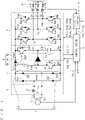
- FIG. 1 is a block diagram illustrating the configuration of a direct power converter to which a control technique according to the present invention can be applied.
- the direct power converter includes a converter 3, a power buffer circuit 4, an inverter 5, and a DC link 7.
- the power buffer circuit 4 functions as the above-described active buffer.
- the converter 3 is connected to a single-phase AC power supply 1, for example, through a filter 2.
- the filter 2 includes a reactor L2 and a capacitor C2.
- the reactor L2 is provided between the converter 3 and one of two output terminals of the single-phase AC power supply 1.
- the capacitor C2 is provided between the two output terminals of the single-phase AC power supply 1.
- the filter 2 removes, from a current, a high-frequency component mainly derived from a switching operation of the inverter 5.
- the filter 2 may be omitted or may be provided between the converter 3 and the power buffer circuit 4.
- the position of the filter 2 will be described below in a second modification. For the sake of simplicity, the function of the filter 2 will be disregarded in the following description.
- the DC link 7 includes DC power supply lines LH and LL.
- the converter 3 adopts, for example, a diode bridge, and includes diodes D31 to D34.
- ; Vin Vm ⁇ sin( ⁇ t)), and outputs the rectified voltage Vrec between the DC power supply lines LH and LL.
- ; Vin Vm ⁇ sin( ⁇ t)
- a potential applied to the DC power supply line LH is higher than a potential applied to the DC power supply line LL.
- An input current Iin flows from the single-phase AC power supply 1 into the converter 3.
- ; Iin Im ⁇ sin( ⁇ t)).
- the power buffer circuit 4 includes a discharge circuit 4a, a charge circuit 4b, and a current blocking circuit 4c, and supplies power to and receives power from the DC link 7.
- the discharge circuit 4a includes a capacitor C4 as a buffer capacitor.
- the charge circuit 4b boosts the rectified voltage Vrec to charge the capacitor C4.
- the current blocking circuit 4c blocks a current flowing from the discharge circuit 4a toward the charge circuit 4b.
- the discharge circuit 4a further includes a diode D42 and a transistor (here, an insulated gate bipolar transistor: hereinafter abbreviated as "IGBT”) Sc connected in antiparallel to the diode D42.
- the transistor Sc is connected in series to the capacitor C4 between the DC power supply lines LH and LL and is closer to the DC power supply line LH than the capacitor C4 is.
- antiparallel connection means parallel connection in which forward directions are opposite to each other.
- the forward direction of the transistor Sc is a direction from the DC power supply line LL toward the DC power supply line LH
- the forward direction of the diode D42 is a direction from the DC power supply line LH toward the DC Power supply line LL.
- the transistor Sc and the diode D42 can collectively be regarded as a single switch element (switch Sc). Conduction of the switch Sc causes the capacitor C4 to discharge and supply power to the DC link 7.
- the charge circuit 4b includes, for example, a diode D40, a reactor L4, and a transistor (here, an IGBT) Sl.
- the diode D40 includes a cathode and an anode. The cathode is connected between the switch Sc and the capacitor C4. This configuration is known as a so-called boost chopper.
- the reactor L4 is connected between the DC power supply line LH and the anode of the diode D40.
- the transistor Sl is connected between the DC power supply line LL and the anode of the diode D40.
- the transistor Sl is connected in antiparallel to a diode D41.
- the transistor Sl and the diode D41 can collectively be regarded as a single switch element (switch Sl). Specifically, the forward direction of the transistor Sl is a direction from the DC power supply line LH toward the DC power supply line LL, and the forward direction of the diode D41 is a direction from the DC power supply line LL toward the DC power supply line LH.
- the capacitor C4 is charged by the charge circuit 4b to generate a voltage Vc across the capacitor C4, the voltage Vc being higher than the rectified voltage Vrec. Specifically, a current is caused to flow from the DC power supply line LH to the DC power supply line LL via the switch Sl to accumulate energy in the reactor L4. Subsequently, the switch Sl is turned off, so that the energy is accumulated in the capacitor C4 via the diode D40.
- the diode D42 ensures a reverse breakdown voltage when the voltage Vc across the capacitor C4 is lower than the rectified voltage Vrec, and functions to cause a current flowing back from an inductive load 6 to the DC link 7 to perform reverse conduction when the inverter 5 abnormally stops.
- the diode D41 is exemplified as a diode for bringing a reverse breakdown voltage and reverse conduction and as a diode built in the transistor Sl which is an IGBT, but the diode D41 does not play a part in a circuit operation.
- the current blocking circuit 4c is provided on the DC power supply line LH between the charge circuit 4b and the discharge circuit 4a.
- a diode D43 serves as the current blocking circuit 4c.
- the anode of the diode D43 is connected to the reactor L4 on the opposite side of the switch Sl (i.e., on the converter 3 side).
- the cathode of the diode D43 is connected to the switch Sc on the opposite side of the capacitor C4 (i.e., on the inverter 5 side).
- the current blocking circuit 4c is known from, for example, Patent Document 5.
- the inverter 5 converters a DC voltage between the DC power supply lines LH and LL into an AC voltage and outputs the AC voltage to output terminals Pu, Pv, and Pw.
- the inverter 5 includes six switching elements Sup, Svp, Swp, Sun, Svn, and Swn.
- the switching elements Sup, Svp, and Swp are connected between the output terminals Pu, Pv, and Pw, respectively, and the DC power supply line LH.
- the switching elements Sun, Svn, and Swn are connected between the output terminals Pu, Pv, and Pw, respectively, and the DC power supply line LL.
- the inverter 5 is a so-called voltage source inverter and includes six diodes Dup, Dvp, Dwp, Dun, Dvn, and Dwn.
- Each of the diodes Dup, Dvp, Dwp, Dun, Dvn, and Dwn is arranged such that the cathode thereof is directed toward the DC power supply line LH and the anode thereof is directed toward the DC power supply line LL.
- the diode Dup is connected in parallel to the switching element Sup between the output terminal Pu and the DC power supply line LH.
- the diodes Dvp, Dwp, Dun, Dvn, and Dwn are connected in parallel to the switching elements Svp, Swp, Sun, Svn, and Swn, respectively.
- the output terminals Pu, Pv, and Pw output load currents iu, iv, and iw, respectively.
- These load currents constitute a three-phase AC current.
- IGBTs are adopted as the switching elements Sup, Svp, Swp, Sun, Svn, and Swn.
- the inductive load 6 is, for example, a rotary machine, and is illustrated as an equivalent circuit representing an inductive load. Specifically, a reactor Lu and a resistor Ru are connected in series to each other, and one end of this series structure is connected to the output terminal Pu. Similar series structures are obtained for reactors Lv and Lw and resistors Rv and Rw. The other ends of these series structures are connected to each other.
- a velocity detector 9 detects the load currents iu, iv, and iw flowing through the inductive load 6 and provides a control device 10 for the direct power converter with a rotational angular velocity ⁇ m, a q-axis current Iq, and a d-axis current Id (to be precise, information representing them; the same applies hereinafter) that are obtained from the load currents iu, iv, and iw.
- the current Ish is an instantaneous value of a current flowing through the inverter 5 and is measured in either the DC power supply line LL or LH by using a known technique.
- the current il is a reactor current flowing through the reactor L4 and corresponds to the above-described buffer current.
- the reactor current il is measured by, for example, a known current protecting device.
- the configuration for obtaining the currents Ish and il is a known technique and thus the illustration thereof is omitted here.
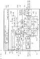
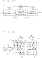
- FIG. 2 is a block diagram exemplifying the configuration of the control device 10.
- the control device 10 includes an inverter controller 101, a discharge controller 102, and a charge controller 103.
- the inverter controller 101 outputs inverter control signals SSup, SSvp, SSwp, SSun, SSvn, and SSwn on the basis of a discharge duty dc', a rectification duty drec', and command values of voltages (hereinafter also referred to as "voltage command values") Vu ⁇ , Vv ⁇ , and Vw ⁇ output from the inverter 5, which will be described below.
- the inverter control signals SSup, SSvp, SSwp, SSun, SSvn, and SSwn control the operations of the switching elements Sup, Svp, Swp, Sun, Svn, and Swn, respectively.
- the inverter controller 101 further includes an amplitude modulation command unit 1012, a multiply-accumulate operation unit 1013, a comparing unit 1014, and a logical operation unit 1015.
- the amplitude modulation command unit 1012 controls an operation of the multiply-accumulate operation unit 1013 on the basis of the discharge duty dc' and the rectification duty drec'.
- the multiply-accumulate operation unit 1013 (only the signs of multipliers are illustrated for the sake of simplicity) performs multiply-accumulate operation between the voltage command values Vu ⁇ , Vv ⁇ , and Vw ⁇ , and the discharge duty dc' and the rectification duty drec', thereby generating signal waves M.
- the comparing unit 1014 outputs results of comparison in value between the signal waves M and a carrier CA to the logical operation unit 1015.
- the logical operation unit 1015 performs logical operation on the results of comparison and outputs the inverter control signals SSup, SSvp, SSwp, SSun, SSvn, and SSwn.
- the discharge controller 102 includes a duty calculating unit 1021, a comparator 1022, and a duty correcting unit 1023.
- the duty calculating unit 1021 receives the phase ⁇ , the amplitude Vm, a command value Vc ⁇ of the voltage Vc across the capacitor C4, and a command value Vdc ⁇ of a DC voltage Vdc described below, and calculates an original discharge duty dc and an original rectification duty drec.
- the duty correcting unit 1023 corrects the original discharge duty dc and the original rectification duty drec to obtain the discharge duty dc' and the rectification duty drec'.
- the duty calculating unit 1021 and the duty correcting unit 1023 can collectively be regarded as a duty generating unit that generates the discharge duty dc' and the rectification duty drec'.
- the comparator 1022 compares the discharge duty dc' with the carrier CA to generate a discharge switch signal SSc for bringing the switch Sc into conduction.
- the charge controller 103 includes a switch control signal generating unit 1031 that generates a control signal SSl for controlling ON and OFF of the switch Sl.
- the switch control signal generating unit 1031 is known from Non-Patent Documents 4 and 5, and thus the details thereof is omitted here but will be briefly described below.
- the switch control signal generating unit 1031 generates the control signal SSl on the basis of an output power Pout, which is instantaneous power output from the inverter 5, and the amplitude Vm.
- a converter input power Pin which is instantaneous power input to the converter 3, is expressed by the following Equation (1), with an amplitude Im of the input current Iin being introduced and an input power factor being 1.
- the converter input power Pin has an AC component (-1/2) ⁇ Vm ⁇ Im ⁇ cos(2 ⁇ t) represented by the second term of the rightmost side of Equation (1) (hereinafter also referred to as an "AC component Pin ⁇ ").
- AC component Pin ⁇ the converter input power Pin may also be referred to as a ripple power Pin.
- the power converter illustrated in FIG. 1 can be grasped as follows.
- the converter 3 receives the single-phase AC voltage Vin and outputs the ripple power Pin.
- the power buffer circuit 4 receives an instantaneous power PI (hereinafter also referred to as a "receiving power Pl") from the DC link 7 and outputs an instantaneous power Pc (hereinafter also referred to as a "supply power Pc") to the DC link 7.
- FIG. 3 is a block diagram schematically illustrating the input and output of power to and from the direct power converter illustrated in FIG. 1 .
- An instantaneous power Pbuf subjected to buffering (hereinafter also referred to as a "buffering power Pbuf") is equal to a power difference (Pc - PI) obtained by subtracting the receiving power PI from the supply power Pc.
- An instantaneous power Prec transmitted from the converter 3 toward the inverter 5 is equal to a power difference (Pin - PI).
- Pdc Prec + Pc holds.
- FIG. 4 illustrates an equivalent circuit of the direct power converter illustrated in FIG. 1 .
- the equivalent circuit is introduced in, for example, Patent Documents 1 and 2.
- a current irec1 is equivalently represented as a current irec1 that flows via a switch Srec when the switch Srec is conducting.
- a discharge current ic is equivalently represented as a current ic that flows via the switch Sc when the switch Sc is conducting.
- a current flowing into the inductive load 6 via the inverter 5 when the output terminals Pu, Pv, and Pw are connected in common to either the DC power supply line LH or LL in the inverter 5 is equivalently represented as a zero-phase current iz that flows via a switch Sz when the switch Sz is conducting.
- FIG. 4 illustrates the reactor L4, the diode D40, and the switch Sl that constitute the charge circuit 4b, and also illustrates the reactor current il flowing through the reactor L4.
- the duty drec' is a duty for setting a time period over which the converter 3 is connected to the DC link 7 and a current is allowed to flow through the inverter 5, and is thus the rectification duty drec' described above.
- the duty dc' is a duty at which the capacitor C4 discharges, and is thus the discharge duty dc' described above.
- the duty dz' is a duty at which the zero-phase current iz always flows regardless of an output voltage in the inverter 5, and thus may be referred to as a zero duty dz'.
- a DC current Idc is a current flowing into the inductive load 6 via the inverter 5 and can be calculated from the current Ish in a manner described below.
- the currents irec1, ic, and iz are obtained by multiplying the duties drec', dc', and dz', respectively, by the DC current Idc.
- the currents irec1, ic, and iz are average values in the switching periods of the switches Srec, Sc, and Sz, respectively.
- the duties drec', dc', and dz' can also be regarded as current distribution factors of the DC current Idc to the currents irec1, ic, and iz, respectively.
- the converter 3 is unable to actively perform switching at the rectification duty drec'.
- the inverter 5 and the switch Sc perform switching in accordance with the zero duty dz' and the discharge duty dc', respectively, thereby being able to obtain the current irec1.
- the inverter 5 In a time period over which the zero-phase current iz flows, the inverter 5 is unable to use a DC voltage in the DC link 7. Thus, the DC voltage in the DC link 7, used for supplying power to the inverter 5 holds significance in power conversion. In other words, an instantaneous DC voltage that is not used by the inverter 5 for power conversion does not hold significance.
- the DC current Idc With the DC voltage Vdc holding significance in power conversion being introduced and Equation (2) being considered, the DC current Idc can be expressed by the following Equation (3).
- the DC voltage Vdc can also be grasped as a voltage to be applied to the DC link 7 as an average value of maximum values of the voltage that the inverter 5 can output in the period of controlling switching of the switches Sc and Sl and the inverter 5.
- the inverter 5 is insulated from either the DC power supply line LL or LH during a time period corresponding to the zero duty dz' although the inverter 5 may contribute to the voltage of the DC link 7 at a ratio represented by the zero duty dz'.
- the DC voltage Vdc is illustrated as a voltage that is generated across a current source Idc (that supplies the DC current Idc) representing the inverter 5 and the inductive load 6.
- equations using the amplitude Im of the input current are used, but it is not always necessary to measure the amplitude Im.
- the inverter input power Pdc can be calculated in the manner described below.
- Equation (5) A power equation on the dq axes is typically expressed by Equation (5).
- V ⁇ and I represent a command value of a voltage applied to the AC load and a current flowing through the AC load, respectively. These are AC, and thus a dot representing a complex number is attached on each of the symbols V ⁇ and I.
- the q-axis voltage ideally follows its command value, that is, the q-axis voltage command value Vq ⁇
- the d-axis voltage ideally follows its command value, that is, the d-axis voltage command value Vd ⁇ .
- Equation (6) Vd ⁇ ⁇ Id + Vq ⁇ ⁇ Iq
- control of making a ripple (AC component) zero of Equation (6) enables control of realizing Equations (3) and (4) to be performed.
- FIG. 5 An example of a configuration for performing the foregoing control is illustrated in FIG. 5 as a block diagram. This configuration is provided in, for example, a configuration illustrated as the output voltage command generating unit 1011 in FIG. 2 .
- Trigonometric function values cos ⁇ ⁇ and -sin ⁇ ⁇ are calculated from a current phase command value ⁇ ⁇
- a q-axis current command value Iq ⁇ and a d-axis current command value Id ⁇ are generated from the trigonometric function values cos ⁇ ⁇ and -sin ⁇ ⁇ and a current command value Ia ⁇ .
- the q-axis voltage command value Vq ⁇ and the d-axis voltage command value Vd ⁇ are calculated on the basis of the rotational angular velocity ⁇ m of the rotary machine, a field magnetic flux ⁇ a of the rotary machine, a d-axis inductance Ld and a q-axis inductance Lq of the rotary machine, the q-axis current command value Iq ⁇ , the d-axis current command value Id ⁇ , the q-axis current Iq, and the d-axis current Id.
- the voltage command values Vu ⁇ , Vv ⁇ , and Vw ⁇ for controlling the inverter 5 are generated.
- the velocity detector 9 detects the load currents iu, iv, and iw flowing through the inductive load 6 and supplies the control device 10 with the rotational angular velocity ⁇ m obtained from the load currents, the q-axis current Iq, and the d-axis current Id.
- a DC power calculating unit 711 receives the q-axis voltage command value Vq ⁇ , the d-axis voltage command value Vd ⁇ , the q-axis current Iq, and the d-axis current Id, calculates the inverter input power Pdc on the basis of Equation (6) given above, and supplies a calculation result to a ripple extracting unit 712.
- the ripple extracting unit 712 extracts and outputs an AC component of Equation (6).
- a high-pass filter HPF serves as the ripple extracting unit 712.
- a PI processing unit 716 performs proportional-integral control on the AC component, and a value obtained thereby is output to a subtracter 715.
- the subtracter 715 performs a process of correcting the current command value Ia ⁇ in a normal process by using the output of the PI processing unit 716. Specifically, as a normal process for calculating the current command value Ia ⁇ , a subtracter 701 calculates a deviation between the rotational angular velocity ⁇ m and the command value ⁇ m ⁇ thereof. The deviation is subjected to proportional-integral control by a PI processing unit 702, and the current command value Ia ⁇ is once calculated. Subsequently, the subtracter 715 performs a process of decreasing the current command value Ia ⁇ with the output from the PI processing unit 716.
- the above-described known technique is applied to the current command value Ia ⁇ corrected in this manner by a processing unit 71, so that the q-axis voltage command value Vq ⁇ and the d-axis voltage command value Vd ⁇ are generated.
- control is performed by giving feedback on the q-axis voltage command value Vq ⁇ and the d-axis voltage command value Vd ⁇ , and the q-axis current Iq and the d-axis current Id, so that the AC component of the inverter input power Pdc converges to zero.
- the rectification duty drec' and the discharge duty dc' are determined without particularly drawing a distinction between a reception period and a supply period in the present embodiment.
- the original rectification duty drec and the original discharge duty dc are once defined by Equations (7) and (8), respectively.
- the command value Vdc ⁇ of the DC voltage Vdc can be used as the DC voltage Vdc. That is, the DC voltage Vdc will be hereinafter handled as a predetermined voltage.
- drec Vdc Vm ⁇ sin ⁇ t
- Vdc ⁇ Vm 0 ⁇ drec ⁇ 1 is satisfied.
- a setting satisfying 0 ⁇ dc ⁇ 1 is possible when the DC voltage Vdc is set to be smaller than or equal to the command value Vc ⁇ .
- Equation 10 the current irec1 in the case of performing control using the original rectification duty drec is calculated by using the following Equation (10).
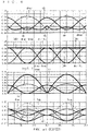
- the top graph shows the duties dc, and dz; the second graph from the top shows the DC voltage Vdc, the voltages drec ⁇ Vrec and dc ⁇ Vc (see Equation (4)) that constitute the DC voltage Vdc, and the DC current Idc; the third graph from the top shows the currents irec, ic, il, and irec1; and the bottom graph shows the instantaneous powers Pin, Pdc, Pbuf, Pc, -Pl, and Prec. It is assumed that the voltage Vc across the capacitor C4 accurately follows the command value Vc ⁇ .
- the horizontal axis represents the phase ⁇ t, with "degrees" being used as the unit.
- the currents Idc, irec, ic, il, and irec1 are converted by using an amplitude Im of ⁇ 2.
- the instantaneous powers Pin, Pout, Pbuf, Pc, -Pl, and Prec are calculated as the products of the voltages converted in the above-described manner and currents.
- FIG. 6 exemplifies a case where the reactor current il has a value il0, where the waveform of the current irec exhibits an absolute value of a sine wave.
- the direct power converter is controlled by using the rectification duty drec' obtained by correcting the original rectification duty drec as described below.
- the current irec1 is decreased in response to a requirement of cancelling out an influence on the input current Iin when the reactor current il is larger than the value il0.
- the rectification duty drec' is decreased to be smaller than the original rectification duty drec.
- Equation (12) the relationship of the following Equation (12) is established in view of the continuity of current.
- Equation (12) Deformation of Equation (12) produces the following Equation (13).
- the second term in the square brackets (the symbol "[" and the symbol "]") of the rightmost side is a correction term for the original rectification duty drec.
- the adoption of the rectification duty drec' decreases distortion of the input current Iin from a sinusoidal waveform regardless of the waveform of the reactor current il.
- the direct power converter is controlled by using the discharge duty dc' obtained by correcting the original discharge duty dc as will be described below.
- Equation (16) is obtained from Equations (14) and (15).
- Equation (18) is obtained from Equations (16) and (17).
- the second term in the square brackets (the symbol "[" and the symbol "]") of the right side is a correction term for the original discharge duty dc.
- the correction term is a value obtained by adding a first value to the original discharge duty dc.
- the first value is a value obtained by dividing a second value by the command value Vc ⁇ .
- the second value is a value obtained by subtracting the DC voltage Vdc from the product of the ratio (il/Idc) and the rectified voltage Vrec.
- dc ′ dc + dc + il Idc ⁇ Vm ⁇ sin ⁇ t ⁇ Vdc Vc ⁇
- the adoption of the discharge duty dc' smooths the output power Pout and removes a ripple component therefrom regardless of the waveform of the reactor current il.
- the corrections expressed by Equations (13) and (18) are realized by the duty correcting unit 1023.
- the corrections require the DC voltage Vdc, which is calculated from the original rectification duty drec and the original discharge duty dc, the amplitude Vm and the phase ⁇ , and the command value Vc ⁇ , as expressed by Equation (9).
- the command value Vdc ⁇ may be used.
- Equations (13) and (18) are performed on the basis of the ratio (il/Idc). Furthermore, the amplitude Im of the input current is unnecessary not only for generating the original rectification duty drec and the original discharge duty dc but also for performing correction to obtain the rectification duty drec' and the discharge duty dc'.
- a period T0 is one period of a carrier CA.
- Time periods ⁇ 4 and ⁇ 6 respectively represent the lengths of time periods over which a first state and a second state are realized in the period T0.
- the first state and the second state will be described while focusing attention on a period in which the switching element Swp is continuously in an OFF state and the switching element Swn is continuously in an ON state in the inverter 5 in one period of the carrier CA.
- the first state is a state in which the switching elements Sup and Svn are in an ON state and the switching elements Sun and Svp are in an OFF state.
- the second state is a state in which the switching elements Sup and Svp are in an ON state and the switching elements Sun and Svn are in an OFF state. It is known that Equation (20) holds when the phase ⁇ v of the voltage output from the inverter 5 and a coefficient of 0 ⁇ k ⁇ 1 are introduced (see, for example, Patent Document 4). [Math.
- Equation (21) holds.
- iw Io ⁇ cos ⁇ i + 2 ⁇ / 3
- the current Ia in Equation (22) is used as the DC current Idc.
- the period T0 is one period of the carrier CA.
- the time periods ⁇ 4 and ⁇ 6 respectively represent the lengths of time periods over which the first state and the second state are realized in the period T0.
- Currents Ish(t4) and Ish(t6) respectively represent the values of the current Ish measured at time t4 and time t6.
- Time t4 and time t6 are respectively selected from the time points at which the first state and the second state are realized. [Math. 22]
- Ia ⁇ 4 ⁇ Ish t 4 + ⁇ 6 ⁇ Ish t 6 To
- the load current iu flows from the output terminal Pu to the inductive load 6 and flows from the output terminals Pv and Pw to the DC power supply line LL.
- the load currents iu and iv flow from the output terminals Pu and Pv, respectively, to the inductive load 6, and flow from the output terminal Pw to the DC power supply line LL.
- Equation (22) is deformed into the following Equation (24) by using Equations (20), (21), and (23).
- ⁇ ⁇ v - ⁇ i is the phase difference between the voltage and current output from the inverter 5, and thus cosy represents the power factor of the inverter 5.
- Equation (25) holds when the power factor cosy is used.
- the calculation based on Equation (22) is executed by a link current calculating unit 1024 included in the discharge controller 102. Since the period T0 is a preset value and the time periods ⁇ 4 and ⁇ 6 can be obtained from the signal waves M, the current Ish and the signal waves M are input to the link current calculating unit 1024, and the DC current Idc is calculated.
- FIG. 7 is a graph showing the waveform of the reactor current il when simple switching is adopted. Here, a region where the phase ⁇ t is 0 to 180 degrees is shown. The waveform of the value il0 is also shown for reference.
- FIG. 10 illustrates the relationship among a value Ts corresponding to the time period over which the switch Sl is conducting, the voltage Vc across the capacitor, a power factor, and output power.
- the inductance of the reactor L4 is 1 H
- Vm 1 V
- Vc 1.14 V
- 45 mW is adopted as the power that makes the power factor maximum.
- Ts 0.194. This corresponds to a phase of ⁇ ⁇ 70 (degrees).
- the reactor current il increases when the phase ⁇ t is 0 to 70 degrees.
- the reactor current il decreases when the phase ⁇ t is 70 to 180 degrees, and keeps a value of 0 after reaching 0 even if the phase ⁇ t proceeds.
- the phase at which the reactor current il decreases to reach a value of 0 is about 170 degrees.
- the power is calculated to be 1/2 ⁇ 2.
- Non-Patent Document 4 a more specific waveform of the reactor current il is calculated.
- il Ip ⁇ (1 - cos( ⁇ t)).
- il Ip ⁇ (1 - cos( ⁇ t)) - (Vc/L) ⁇ ( ⁇ t- ⁇ )/ ⁇ .
- L is the inductance of the reactor L4.
- the waveform illustrated in FIG. 7 is adopted as the waveform of the reactor current il.
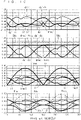
- FIG. 8 illustrates the quantities similarly to FIG. 6 .
- the top graph shows the duties drec', dc', and dz';
- the second graph from the top shows the DC voltage Vdc, the voltages drec' ⁇ Vrec and dc' ⁇ Vc (see Equation (19)) that constitute the DC voltage Vdc, and the DC current Idc;
- the third graph from the top shows the currents irec, ic, il, and irec1;
- the bottom graph shows the instantaneous powers Pin, Pdc, Pbuf, Pc, -Pl, and Prec.
- control using the rectification duty drec' and the discharge duty dc' makes not only the inverter input power Pdc but also the DC voltage Vdc and the DC current Idc constant, and also causes the waveform of the current irec to exhibit the absolute value of a sine wave. Accordingly, it is understood that the waveform of the input current Iin is sinusoidal.
- the power buffer circuit 4 functions as a power buffer.
- the zero duty can be made non-negative by using another method.
- the waveform illustrated in FIG. 7 is adopted as the waveform of the reactor current il.
- the quantities are illustrated in FIG. 10 similarly to FIG. 8 .
- Such a lower DC voltage Vdc makes the original rectification duty drec and the original discharge duty dc lower (see Equations (7) and (8)) and makes the rectification duty drec' and the discharge duty dc' lower accordingly, and the minimum value of dz' can be 0 in all the phases in the control using these duties.
- Non-Patent Document 5 exemplifies the case of obtaining a DC voltage of 270 V from a power supply of 100 V (an effective voltage value of 100 V in single phase) by using voltage-doubling rectification.
- Vc 270/2/(100 ⁇ ⁇ 2) ⁇ 0.95.
- the power that makes the power factor maximum is about 30 mW.
- the value of the inductance is 6.2 mH.
- the power is 45/30 times in the present embodiment.
- Vm 230 V.
- an influence of full-wave rectification adopted in the present embodiment on the inductance is (230/100) 2 times.
- a necessary value of the inductance is 6.5 [mH] ⁇ 45/30 ⁇ (230/100) 2 ⁇ 52 [mH].
- Non-Patent Document 5 the adoption of the simple switching exemplified in Non-Patent Document 5 in the power buffer circuit 4 in which a boost operation is performed is likely to increase the inductance of the reactor L4 (about twice in the above example).
- Non-Patent Document 4 introduces a technique for delaying the starting time of conduction of a switching element. According to this technique, a large power factor can be obtained even when the inductance is small.
- FIG. 11 is a graph showing the relationship between an inductance L and a power factor when a power of 1.84 kW (an effective voltage value of 230 V and an effective current value of 8 A) is adopted in the present embodiment on the basis of Non-Patent Document 4.
- the frequency of the single-phase AC voltage Vin is 50 Hz.
- the inductance L has a value that makes the power factor maximum.
- the data that makes the power factor maximum is plotted in white.
- the power factor decreases as the conduction start phase increases.
- the value of the inductance L that makes the power factor maximum decreases as the conduction start phase increases.
- the power factor is maximum when the inductance L is 51.37 mH.
- the effective voltage value is 230 V
- the effective current value is 8A
- the direct power converter according to the present embodiment is adopted to a compact air conditioner used with a power of, for example, 2 kW or less, it is desired that the inductance of the reactor L4 be set to 15 mH to 30 mH and a compact component be adopted accordingly.
- the conduction start phase when an inductance L of about 28 mH is adopted, it is desired that the conduction start phase be 45 degrees (see the graph G3) from the viewpoint of a flat power factor characteristic. However, from the viewpoint of increasing the power factor, it is desired that the conduction start phase be 36 degrees (see the graph G2). In the description given below, the conduction start phase is 36 degrees in all the cases.
- FIG. 12 to FIG. 14 each include graphs showing an operation of the direct power converter illustrated in FIG. 1 .
- graphs are drawn with Vc being 1.14 Vm, the amplitude Im being ⁇ 2, and the amplitude Vm being 1.
- a power of 1.84 kW (an effective voltage value of 230 V and an effective current value of 8 A) is adopted, and the inductance L is set to 28.54 mH.
- the conduction start phase is 36 degrees, and thus the phase at which the switch Sl shifts from a conduction state to a non-conduction state is about 68 (360 ⁇ 0.19) degrees.
- the reactor current il has a maximum value. After that, the reactor current il decreases as the phase increases, and the reactor current il becomes 0 at about 155 (360 ⁇ 0.430) degrees.
- the cases illustrated in FIG. 8 to FIG. 11 correspond to a case where a power of 1.84 kW (an effective voltage value of 230 V and an effective current value of 8 A) is adopted and the inductance L is set to 51.37 mH.
- FIG. 12 illustrates an operation in a case where the rectification duty drec' is set on the basis of Equation (13), the discharge duty dc' is set on the basis of Equation (18), the zero duty dz' is set by 1 - drec' - dc', and Vdc is set to 0.86 Vm, as in the conditions used in FIG. 8 .
- FIG. 12 illustrates quantities similarly to FIG. 8 .
- the top graph shows the duties drec', dc', and dz';
- the second graph from the top shows the DC voltage Vdc, the voltages drec' ⁇ Vrec and dc' ⁇ Vc that constitute the DC voltage Vdc, and the DC current Idc;
- the third graph from the top shows the currents irec, ic, il, and irec1;
- the bottom graph shows the instantaneous powers Pin, Pdc, Pbuf, Pc, -Pl, and Prec.
- FIG. 13 illustrates quantities similarly to FIG. 12 .
- the DC voltage Vdc is under 0.86 Vm, and the waveform of the current irec is distorted from the absolute value of a sine wave.
- the minimum value of the DC voltage Vdc is 0.72 Vm in FIG. 13 , which is lower than 0.80 Vm, which is the minimum value in FIG. 9 .
- the inductance L is 28.54 mH and the conduction start phase is 36 degrees, and thus it is necessary to decrease Vdc to 0.69 Vm to satisfy 1 - drec' - dc' ⁇ 0.
- the cause of a decrease in the minimum value of the DC voltage Vdc that fluctuates and a decrease in the maximum value of the DC voltage Vdc that can be constant may be that a decrease in the inductance L causes a shorter time period over which the reactor current il flows and that the reactor current il contains many harmonic components (specifically, the third- or higher-order odd harmonic components of the frequency of the single-phase AC voltage Vin).
- Harmonics are controlled by, for example, the standard IEC 61000-3-2.
- the magnitude of a third-order harmonic component is larger than that in the standard IEC 61000-3-2.
- irec irec1 + il (see FIG. 1 and FIG. 4 )
- the third-order harmonic component of the reactor current il is reflected as is in the current irec and affects the third-order harmonic component of the input current Iin accordingly.
- a technique for reducing harmonics contained in the reactor current il will be considered.
- FIG. 15 is a graph showing the waveform of the reactor current il exemplified in FIG. 12 to FIG. 14 in the half-period of the single-phase AC voltage Vin, specifically, when the phase ⁇ t is 0 to 180 degrees. Also when the phase ⁇ t is 180 to 360 degrees, the reactor current il has the same waveform. As in the above case, a power of 1.84 kW (an effective voltage value of 230 V and an effective current value of 8 A) is adopted, and the inductance L is set to 28.54 mH. The reactor current il is shown with the amplitude Im being ⁇ 2.
- a third-order harmonic component of up to an effective value of 2.30 A is allowed under the condition of a rated voltage of 230 V.
- the reactor current il illustrated in FIG. 15 contains a third-order harmonic component of an effective value of 2.87 A when the effective voltage value is 230 V, and harmonic components of other orders are within an allowable range of the standard IEC 61000-3-2.
- a rectification duty drec a discharge duty dc
- a zero duty dz a zero duty dz
- Equation (12) the amount of correction il' of the reactor current il is the amount of reduction (0.571 A) in the third-order harmonic component of the reactor current il.
- Equation (12) the amount of deviation of the reactor current il from the value il0, (il - i0) is used.
- the rectification duty drec' may be replaced with the rectification duty drec" and the amount of deviation (il - i0) may be replaced with a value (-il') formally in Equation (12).
- Equation (27) is obtained in view of Equation (7).
- Equation (28) is obtained.
- Equation (29) is obtained in view of Equation (8).
- Equation (30) Calculation is performed similarly to Equation (19) by using the rectification duty drec" and the discharge duty dc" obtained in this manner, so that Equation (30) is obtained. That is, it is understood that the adoption of the rectification duty drec" and the discharge duty dc" enables control for making the DC voltage Vdc constant.
- FIG. 17 includes graphs showing quantities in a case where the rectification duty drec" and the discharge duty dc" are set by Equations (27) and (29), respectively, and the zero duty dz" is set by 1 - drec" - dc", with the values of specifications corresponding to those in the description using FIG. 12 . It is understood that there is a phase region where dz" ⁇ 0.
- the zero duty dz" illustrated in FIG. 17 is smaller in the absolute value of a negative value than the zero duty dz' illustrated in FIG. 12 .
- the minimum value of the DC voltage Vdc is larger in the case illustrated in FIG. 18 than in the case illustrated in FIG. 13 .
- FIG. 19 includes graphs showing quantities in a case where the rectification duty drec", the discharge duty dc", and the zero duty dz" are set similarly to FIG. 17 .
- the DC voltage Vdc that can be used for power conversion by the inverter 5 is increased, with the harmonics of the input current Iin being reduced and distortion of the waveform of the input current Iin from a sinusoidal waveform being allowed.
- a decrease in the inductance L causes an increase in components of the fifth- or higher-order harmonics of the reactor current il.
- FIG. 20 is a graph showing the waveform of the reactor current il in the half-period of the single-phase AC voltage Vin, specifically, when the phase ⁇ t is 0 to 180 degrees. Also when the phase ⁇ t is 180 to 360 degrees, the reactor current il has the same waveform.
- the phase at which the switch Sl shifts from a conduction state to non-conduction state is about 61 (360 ⁇ 0.17) degrees.
- the reactor current il has a maximum value.
- the reactor current il is 0.
- a third-order harmonic component, a seventh-order harmonic component, and an eleventh-order harmonic component are allowed up to effective values of 2.30 A, 0.77A, and 0.33 A, respectively, under the condition of a rated voltage of 230 V.
- the reactor current il illustrated in FIG. 20 contains a third-order harmonic component of an effective value of 3.66 A, a seventh-order harmonic component of an effective value of 1.17 A, and an eleventh-order harmonic component of an effective value of 0.38 A, and harmonic components of other orders are within an allowable range of the standard IEC 61000-3-2.
- the rectification duties drec' and drec" can be defined as follows: the rectification duties (drec', drec") are set on the basis of the product (Vdc/Vm) ⁇
- the foregoing product represents the original rectification duty drec (see Equation (7)).
- the foregoing "current” is the reactor current il for the rectification duty drec' and is the amount of correction il' for the rectification duty drec".
- the amount of correction il' is the amount of reduction in the harmonic component of the order to be reduced.
- the rectification duty drec' has a value obtained by subtracting the ratio il/Idc from twice the product (Vdc/Vm) ⁇
- the rectification duty drec" has a value obtained by adding the ratio il'/Idc to the product (Vdc/Vm) ⁇
- the discharge duty dc' can be expressed as follows on the basis of Equation (16):
- the discharge duty dc can be expressed as follows on the basis of Equation (29):
- FIG. 24 is a block diagram exemplifying a first configuration of the discharge controller 102 for obtaining the rectification duty drec" and the discharge duty dc" and its vicinity.
- the discharge controller 102 constitutes the control device 10 together with the inverter controller 101 and the charge controller 103 illustrated in FIG. 2 .
- the discharge controller 102 includes an amount-of-correction generating unit 1025 in addition to the duty calculating unit 1021, the comparator 1022, the duty correcting unit 1023, and the link current calculating unit 1024 described using FIG. 2 .
- the duty correcting unit 1023 obtains the rectification duty drec" and the discharge duty dc" from the original rectification duty drec and the original discharge duty dc, respectively, in accordance with Equations (27) and (29) (particularly the first equality in each equation), respectively.
- FIG. 25 is a block diagram exemplifying the configuration of the amount-of-correction generating unit 1025.
- the amount-of-correction generating unit 1025 includes an input current estimating unit 1025a and a correction harmonic table 1025b.
- the correction harmonic table 1025b stores therein a table showing the relationship between the input current Iin and the amount of control of harmonic components, searches the table while adopting the estimated value Is as the input current Iin, and outputs the corresponding amount of correction il'.
- the amount of correction il' is calculated on the basis of the distortion of the input current Iin.
- the reactor current il is not necessary for the control device 10.
- FIG. 26 is a block diagram exemplifying a second configuration of the discharge controller 102 for obtaining the rectification duty drec" and the discharge duty dc" and its vicinity.
- the discharge controller 102 also constitutes the control device 10 together with the inverter controller 101 and the charge controller 103 illustrated in FIG. 2 .
- the discharge controller 102 includes an amount-of-correction generating unit 1026 in addition to the duty calculating unit 1021, the comparator 1022, the duty correcting unit 1023, and the link current calculating unit 1024 described using FIG. 2 .
- the duty correcting unit 1023 obtains the rectification duty drec" and the discharge duty dc" in accordance with Equations (27) and (29) (particularly the first equality in each equation), respectively.
- FIG. 27 is a block diagram exemplifying the configuration of the amount-of-correction generating unit 1026.
- the amount-of-correction generating unit 1026 includes an FFT operation unit 1026a, a correction harmonic selecting unit 1026b, and an inverse FFT operation unit 1026c.
- the FFT operation unit 1026a performs fast Fourier transform on the reactor current il to calculate an amplitude Ilh(n) of each component of the n-th order frequency.
- the correction harmonic selecting unit 1026b selects the order of harmonics exceeding the upper limit that is set for each order.
- the correction harmonic selecting unit 1026b calculates the amount of the amplitude Ilh( ⁇ ) of the ⁇ -th order harmonic component exceeding the upper limit that is set for the ⁇ -th order harmonic, as an amount of correction Il'( ⁇ ) of the ⁇ -th order harmonic.
- An amount of correction Il'( ⁇ ) ( ⁇ ⁇ ⁇ ) of the order that is not selected is 0.
- the inverse FFT operation unit 1026c performs inverse fast Fourier transform by using the amount of correction Il'(n) or the amount of correction Il'( ⁇ ) to calculate the amount of correction il'.
- the amount of correction il' is calculated on the basis of the distortion of the reactor current il (see FIG. 15 and FIG. 20 ).
- FIG. 28 is a circuit diagram illustrating diode bridges 3a and 3b replacing the converter 3 and their vicinity as a first modification of the power converter. This configuration is known from, for example, Non-Patent Document 1.
- the diode bridge 3a includes, like the converter 3 described in the foregoing embodiment, the diodes D31, D32, D33, and D34, which constitute a bridge circuit.
- the diode bridge 3b includes diodes D35, D36, D32, and D34, which constitute a bridge circuit. That is, the diode bridges 3a and 3b share the diodes D32 and D34.
- the DC power supply line LH described in the foregoing embodiment is replaced with two DC power supply lines LH1 and LH2.
- the DC power supply line LL is connected to the anodes of the diodes D32 and D34, the switch Sl on the opposite side to the reactor L4, the capacitor C4 on the opposite side to the switch Sc, and the inverter 5, as in the foregoing embodiment.
- the DC power supply line LH1 is connected to the cathodes of the diodes D31 and D33 in common, the switch Sc on the opposite side to the capacitor C4, and the inverter 5, like the DC power supply line LH.
- the DC power supply line LH2 is connected to the cathodes of the diodes D35 and D36 in common, and the reactor L4 on the opposite side to the switch S1.
- the supply of power to the DC power supply line LH1 from the diode bridge 3a and the discharge circuit 4a is equivalent to the supply of power to the DC power supply line LH in the foregoing embodiment from the converter 3 and the discharge circuit 4a.
- the supply of power from the DC power supply line LH2 to the charge circuit 4b via the diode bridge 3b is equivalent to the supply of power from the DC power supply line LH in the foregoing embodiment to the charge circuit 4b via the converter 3 (the reception of power by the charge circuit 4b).
- the path for supplying power and the path for receiving power are different from each other, and thus the current blocking circuit 4c according to the foregoing embodiment is not necessary in the first modification.
- the current blocking circuit 4c also has a function of blocking the current flowing from the discharge circuit 4a toward the converter 3.
- the filter 2 can be disposed between the converter 3 and the current blocking circuit 4c.
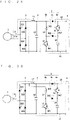
- FIG. 29 and FIG. 30 are circuit diagrams each illustrating the configuration on the single-phase AC power supply 1 side respect to the inverter 5 in a case where the filter 2 is disposed between the converter 3 and the current blocking circuit 4c in the power converter.
- the reactor L4 is connected to the converter 3-side end of the reactor L2.
- the filter 2 may be included in the charge circuit 4b although the filter 2 is disposed between the converter 3 and the current blocking circuit 4c.
- the reactor L2 is provided on the DC power supply line LH, at a position across the reactor L4 from the converter 3.
- the capacitor C2 is connected between the DC power supply lines LH and LL, at a position across the reactor L2 from the converter 3, and constitutes the filter together with the reactor L2.
Landscapes
- Engineering & Computer Science (AREA)
- Power Engineering (AREA)
- Rectifiers (AREA)
- Inverter Devices (AREA)
- Ac-Ac Conversion (AREA)
Claims (8)
- Steuervorrichtung (10) zum Steuern eines Gleichstromwandlers,
wobei der Gleichstromwandler umfasst:eine Gleichstromverbindung (7), einschließlich einer ersten Gleichstrom-Leistungsversorgungsleitung (LH; LH1, LH2) und einer zweiten Gleichstrom-Leistungsversorgungsleitung (LL);einen Wandler (3), der konfiguriert ist, um eine einphasige Wechselstormspannung (Vin) zu empfangen, eine gleichgerichtete Spannung (Vrec), die durch vollwelliges Gleichrichten der einphasigen Wechselstromspannung (Vin) erhalten wird, derart an der Gleichstromverbindung (7) anzulegen, dass die erste Gleichstrom-Leistungsversorgungsleitung (LH; LH1, LH2) ein höheres Potential aufweist als die zweite Gleichstrom-Leistungsversorgungsleitung (LL), und eine Restwelligkeitsleistung (Pin) an die Gleichstromverbindung auszugeben;eine Leistungspufferschaltung (4), die konfiguriert ist, um eine Leistung (Pc, P1) an die Gleichstromverbindung zu liefern und von dieser empfängt; undeinen Wechselrichter (5), der konfiguriert ist, um eine Gleichstromspannung zwischen der ersten Gleichstrom-Leistungsversorgungsleitung und der zweiten Gleichstrom-Leistungsversorgungsleitung in eine Wechselstromspannung zu wandeln,wobei die Steuervorrichtung (10) umfasst:eine Lasterzeugungseinheit (1021, 1023), die konfiguriert ist, um eine korrigierte Gleichrichtungslast drec', die eine Last ist, bei der ein erster Strom irec1 von dem Wandler zu der Gleichstromverbindung fließt, und eine korrigierte Entladelast dc', die eine Last ist, bei der ein zweiter Strom (ic) von der Leistungspufferschaltung zu der Gleichstromverbindung fließt, zu erzeugen; undeine Wechselrichtersteuereinheit (101), die konfiguriert ist, um ein Wechselrichtersteuersignal (SSup, SSvp, SSwp, SSun, SSvn, SSwn), das einen Betrieb des Wechselrichters steuert, auf der Grundlage der korrigierten Gleichrichtungslast drec', der korrigierten Entladelast dc' und eines Regelungswerts (Vu∗, Vv∗, Vw∗) einer Spannung, die von dem Wechselrichter ausgegeben wird, auszugeben,dadurch gekennzeichnet, dassdie korrigierte Gleichrichtungslast drec' erhalten wird gemäß wobei drec eine ursprüngliche Gleichrichtungslast ist, il ein Strom ist, der von der Gleichstromverbindung in die Leistungspufferschaltung (4) eingegeben wird, Idc ein Gleichstrom ist, der durch den Wechselrichter fließt, und ein zweites Verhältnis i1/Idc ein Verhältnis von i1 zu Idc ist,wobei die korrigierte Entladelast dc' erhalten wird gemäß
- Steuervorrichtung (10) zum Steuern eines Gleichstromwandlers,
wobei der Gleichstromwandler umfasst:eine Gleichstromverbindung (7), einschließlich einer ersten Gleichstrom-Leistungsversorgungsleitung (LH; LH1, LH2) und einer zweiten Gleichstrom-Leistungsversorgungsleitung (LL);einen Wandler (3), der konfiguriert ist, um eine einphasige Wechselstormspannung (Vin) zu empfangen, eine gleichgerichtete Spannung (Vrec), die durch vollwelliges Gleichrichten der einphasigen Wechselstromspannung (Vin) erhalten wird, derart an der Gleichstromverbindung (7) anzulegen, dass die erste Gleichstrom-Leistungsversorgungsleitung (LH; LH1, LH2) ein höheres Potential aufweist als die zweite Gleichstrom-Leistungsversorgungsleitung (LL), und eine Restwelligkeitsleistung (Pin) an die Gleichstromverbindung auszugeben;eine Leistungspufferschaltung (4), die konfiguriert ist, um eine Leistung (Pc, P1) an die Gleichstromverbindung zu liefern und von dieser empfängt; undeinen Wechselrichter (5), der konfiguriert ist, um eine Gleichstromspannung zwischen der ersten Gleichstrom-Leistungsversorgungsleitung und der zweiten Gleichstrom-Leistungsversorgungsleitung in eine Wechselstromspannung zu wandeln,wobei die Steuervorrichtung (10) umfasst:eine Lasterzeugungseinheit (1021, 1023), die konfiguriert ist, um eine korrigierte Gleichrichtungslast drec", die eine Last ist, bei der ein erster Strom irec1 von dem Wandler zu der Gleichstromverbindung fließt, und eine korrigierte Entladelast dc", die eine Last ist, bei der ein zweiter Strom ic von der Leistungspufferschaltung zu der Gleichstromverbindung fließt, zu erzeugen; undeine Wechselrichtersteuereinheit (101), die konfiguriert ist, um ein Wechselrichtersteuersignal (SSup, SSvp, SSwp, SSun, SSvn, SSwn), das einen Betrieb des Wechselrichters steuert, auf der Grundlage der korrigierten Gleichrichtungslast drec", der korrigierten Entladelast dc" und eines Regelungswerts (Vu∗, Vv∗, Vw∗) einer Spannung, die von dem Wechselrichter ausgegeben wird, auszugeben, dadurch gekennzeichnet, dass die korrigierte Gleichrichtungslast drec" erhalten wird gemäß wobei drec eine ursprüngliche Gleichrichtungslast ist, Vdc/Vm ein erstes Verhältnis einer vorbestimmten Spannung Vdc zu einer Amplitude Vm der einphasigen Wechselstromspannung ist, |sin(ωt)| ein Absolutwert eines Sinuswerts einer Phase ωt der einphasigen Wechselstromspannung ist, i1' eine Verringerungsmenge einer harmonischen Komponente des Stroms il ist, der von der Gleichstromverbindung in die Leistungspufferschaltung (4) eingegeben wird, und ein zweites Verhältnis i1'/Idc ein Verhältnis von i1' zu einem Gleichstrom Idc ist, der durch den Wechselrichter fließt,wobei die korrigierte Entladelast dc" erhalten wird gemäß
 wobei dc eine ursprüngliche Entladelast ist und Vc∗ ein Regelungswert der Spannung Vc über einen Kondensator (C4) der Leistungspufferschaltung (4) ist.
 - Steuervorrichtung für den Gleichstromwandler nach Anspruch 1, wobeidie Leistungspufferschaltung (4) einschließteine Entladeschaltung (4a), einschließlich des Kondensators (C4) und eines ersten Schalters (Sc, D42), der zwischen der ersten Gleichstrom-Leistungsversorgungsleitung und der zweiten Gleichstrom-Leistungsversorgungsleitung mit dem Kondensator in Reihe geschaltet ist und näher an der ersten Gleichstrom-Leistungsversorgungsleitung ist als es der Kondensator ist, undeine Ladeschaltung (4b), die konfiguriert ist, um den Kondensator zu laden,wobei die Steuervorrichtung (10) konfiguriert ist, um ein Entladeschaltsignal (SSc), das den ersten Schalter leitend macht, auf der Grundlage der korrigierten Entladelast dc' auszugeben.
- Steuervorrichtung für den Gleichstromwandler nach Anspruch 2, wobei die Leistungspufferschaltung (4) einschließteine Entladeschaltung (4a), einschließlich des Kondensators (C4) und eines ersten Schalters (Sc, D42), der zwischen der ersten Gleichstrom-Leistungsversorgungsleitung und der zweiten Gleichstrom-Leistungsversorgungsleitung mit dem Kondensator in Reihe geschaltet ist und näher an der ersten Gleichstrom-Leistungsversorgungsleitung ist als es der Kondensator ist, undeine Ladeschaltung (4b), die konfiguriert ist, um den Kondensator zu laden, wobei die Steuervorrichtung (10) konfiguriert ist, um ein Entladeschaltsignal (SSc), das den ersten Schalter leitend macht, auf der Grundlage der korrigierten Entladelast dc" auszugeben.
- Steuervorrichtung für den Gleichstromwandler nach einem der Ansprüche 3 und 4, wobei die Steuervorrichtung (10) weiter eine Korrekturmengenerzeugungseinheit (1025) umfasst, die konfiguriert ist, um die Verringerungsmenge i1' auf der Grundlage einer harmonischen Komponente eines eingegebenen Stroms (lin), der in den Wandler (3) eingegeben wird, zu erhalten.
- Steuervorrichtung für den Gleichstromwandler nach einem der Ansprüche 3 und 4, wobei die Steuervorrichtung (10) weiter eine Korrekturmengenerzeugungseinheit (1026) umfasst, die konfiguriert ist, um die Verringerungsmenge i1' auf der Grundlage einer harmonischen Komponente des Stroms i1 zu erhalten.
- Steuervorrichtung für den Gleichstromwandler nach einem der Ansprüche 3 bis 6, wobei
die Lasterzeugungseinheit einschließteine Lastberechnungseinheit (1021), die konfiguriert ist, um die ursprüngliche Gleichrichtungslast drec, die ein Produkt des ersten Verhältnisses Vdc/Vm und des Absolutwerts |sin(ωt)| des Sinuswerts ist, und die ursprüngliche Entladelast dc, die ein Produkt des dritten Verhältnisses Vdc/Vc und eines Quadrats (cos2(ωt)) eines Cosinuswerts der Phase ωt der einphasigen Wechselstromspannung ist, zu erhalten, undeine Lastkorrektureinheit (1023), die konfiguriert ist, um Korrektur basierend auf dem zweiten Verhältnis (il/Idc; il'/Idc) durchzuführen, um die korrigierte Gleichrichtungslast (drec'; drec") aus der ursprünglichen Gleichrichtungslast und die korrigierte Entladelast (dc'; dc") aus der ursprünglichen Entladelast zu erhalten. - Steuervorrichtung für den Gleichstromwandler nach einem der Ansprüche 3 bis 7, wobeidie Lastschaltung (4b) einschließteine Diode (D40), einschließlich einer Kathode, die mit dem Kondensator (C4) verbunden ist, und einer Anode,einen Reaktor (L4), der zwischen der ersten Gleichstrom-Leistungsversorgungsleitung (LH; LH1, LH2) und der Anode verbunden ist, undeinen zweiten Schalter (S1, D41), der zwischen der zweiten Gleichstrom-Leistungsversorgungsleitung (LL) und der Anode verbunden ist,wobei die Steuervorrichtung (10) weiter eine Schaltsteuersignal-Erzeugungseinheit (1031) umfasst, die konfiguriert ist, um ein Steuersignal (SS1) zu erzeugen, das bewirkt, dass der zweite Schalter in einer Periode der gleichgerichteten Spannung (Vrec) einmal eingeschaltet und einmal ausgeschaltet wird.
Applications Claiming Priority (2)
| Application Number | Priority Date | Filing Date | Title |
|---|---|---|---|
| JP2016192704 | 2016-09-30 | ||
| PCT/JP2017/034929 WO2018062261A1 (ja) | 2016-09-30 | 2017-09-27 | 直接形電力変換器用の制御装置 |
Publications (3)
| Publication Number | Publication Date |
|---|---|
| EP3522355A1 EP3522355A1 (de) | 2019-08-07 |
| EP3522355A4 EP3522355A4 (de) | 2020-06-03 |
| EP3522355B1 true EP3522355B1 (de) | 2022-10-26 |
Family
ID=61020790
Family Applications (1)
| Application Number | Title | Priority Date | Filing Date |
|---|---|---|---|
| EP17856210.4A Active EP3522355B1 (de) | 2016-09-30 | 2017-09-27 | Steuerungsvorrichtung für einen direktstromwandler |
Country Status (6)
| Country | Link |
|---|---|
| US (1) | US10804811B2 (de) |
| EP (1) | EP3522355B1 (de) |
| JP (1) | JP6265297B1 (de) |
| CN (1) | CN109874384B (de) |
| AU (1) | AU2017337434B2 (de) |
| WO (1) | WO2018062261A1 (de) |
Families Citing this family (15)
| Publication number | Priority date | Publication date | Assignee | Title |
|---|---|---|---|---|
| JP6394741B1 (ja) * | 2017-05-30 | 2018-09-26 | ダイキン工業株式会社 | 電力変換装置、冷凍装置 |
| JP6418287B1 (ja) * | 2017-06-30 | 2018-11-07 | ダイキン工業株式会社 | 直接形電力変換器用制御装置 |
| US11152780B2 (en) * | 2017-08-31 | 2021-10-19 | Eaton Intelligent Power Limited | Adjustable speed drive with integrated solid-state circuit breaker and method of operation thereof |
| JP6993925B2 (ja) * | 2018-04-20 | 2022-01-14 | 株式会社デンソー | 電力変換装置の制御装置 |
| JP6913056B2 (ja) * | 2018-05-29 | 2021-08-04 | 株式会社Soken | 電力変換装置の制御装置 |
| JP6721097B2 (ja) * | 2018-09-27 | 2020-07-08 | ダイキン工業株式会社 | 直接形電力変換器、制御装置 |
| JP7161110B2 (ja) * | 2019-03-14 | 2022-10-26 | ダイキン工業株式会社 | 直接形電力変換器用の制御装置 |
| JP7206491B2 (ja) * | 2019-03-28 | 2023-01-18 | ダイキン工業株式会社 | 直接形電力変換器用の制御装置 |
| JP7436783B2 (ja) * | 2019-09-30 | 2024-02-22 | ダイキン工業株式会社 | 電力変換装置 |
| JP7130024B2 (ja) * | 2020-11-12 | 2022-09-02 | 三菱電機株式会社 | 電力変換装置 |
| CN113612402A (zh) * | 2021-08-09 | 2021-11-05 | 山特电子(深圳)有限公司 | 一种三相逆变控制系统和控制方法 |
| US11664757B1 (en) * | 2022-05-16 | 2023-05-30 | Forcecon Technology Co., Ltd. | Motor control system with adjustable voltage harmonic and method for correcting the motor control system |
| JP7549264B1 (ja) * | 2023-06-23 | 2024-09-11 | ダイキン工業株式会社 | 直接形電力変換回路 |
| WO2026063362A1 (ja) * | 2024-09-18 | 2026-03-26 | ダイキン工業株式会社 | 電力変換装置 |
| CN119872312B (zh) * | 2025-01-18 | 2025-11-18 | 深圳市瑞精创实业有限公司 | 具有自适应电流分配功能的充电桩储能连接器系统及方法 |
Family Cites Families (20)
| Publication number | Priority date | Publication date | Assignee | Title |
|---|---|---|---|---|
| KR100351140B1 (ko) * | 1999-01-08 | 2002-09-09 | 엘지전자주식회사 | 인버터의 역률보정장치 |
| US6636107B2 (en) * | 2000-03-28 | 2003-10-21 | International Rectifier Corporation | Active filter for reduction of common mode current |
| JP3699663B2 (ja) * | 2001-05-24 | 2005-09-28 | 勲 高橋 | インバータ制御方法およびその装置 |
| JP5045716B2 (ja) * | 2009-08-26 | 2012-10-10 | ダイキン工業株式会社 | 単相/三相直接変換装置の制御方法 |
| JP4735761B1 (ja) * | 2010-01-19 | 2011-07-27 | ダイキン工業株式会社 | 電力変換装置 |
| JP5925526B2 (ja) * | 2012-02-29 | 2016-05-25 | サンデンホールディングス株式会社 | モータ制御装置、モータ制御プログラム |
| JP5765287B2 (ja) * | 2012-04-12 | 2015-08-19 | 三菱電機株式会社 | コンバータ制御装置及びコンバータ制御装置を備えた空気調和機 |
| WO2014057883A1 (ja) | 2012-10-10 | 2014-04-17 | ダイキン工業株式会社 | 直接形電力変換装置および直接形電力変換装置の制御方法 |
| JP5804167B2 (ja) | 2013-09-19 | 2015-11-04 | ダイキン工業株式会社 | 電力変換装置 |
| JP5664733B1 (ja) | 2013-09-24 | 2015-02-04 | ダイキン工業株式会社 | 直接形電力変換装置の制御方法 |
| JP5794273B2 (ja) | 2013-10-07 | 2015-10-14 | ダイキン工業株式会社 | 直接形電力変換装置の制御方法 |
| CN106471725B (zh) * | 2014-07-18 | 2018-02-27 | 大金工业株式会社 | 直接型交流电力变换装置 |
| JP5930108B2 (ja) * | 2014-09-25 | 2016-06-08 | ダイキン工業株式会社 | 電力変換装置 |
| JP5874800B1 (ja) | 2014-10-15 | 2016-03-02 | ダイキン工業株式会社 | 直接型電力変換器用制御装置 |
| JP6094615B2 (ja) | 2014-11-18 | 2017-03-15 | ダイキン工業株式会社 | インバータの制御装置 |
| JP5920520B1 (ja) * | 2014-12-17 | 2016-05-18 | ダイキン工業株式会社 | 充放電回路、充放電回路の制御方法、充放電回路の制御装置、及び直接形電力変換器 |
| DE102015200249A1 (de) * | 2015-01-12 | 2016-07-14 | Otto Bihler Handels-Beteiligungs-Gmbh | Versorgungsschaltung zur Versorgung eines Schweißgerätes |
| JP6430028B2 (ja) * | 2015-10-01 | 2018-11-28 | 三菱電機株式会社 | 電力変換装置及びこれを用いた空気調和装置 |
| JP6702209B2 (ja) * | 2017-01-26 | 2020-05-27 | 株式会社デンソー | 電力変換装置 |
| WO2019088678A1 (en) * | 2017-11-02 | 2019-05-09 | Samsung Electronics Co., Ltd. | Air conditioner and rectifier |
-
2017
- 2017-09-26 JP JP2017184866A patent/JP6265297B1/ja active Active
- 2017-09-27 CN CN201780059229.4A patent/CN109874384B/zh active Active
- 2017-09-27 US US16/336,586 patent/US10804811B2/en active Active
- 2017-09-27 EP EP17856210.4A patent/EP3522355B1/de active Active
- 2017-09-27 WO PCT/JP2017/034929 patent/WO2018062261A1/ja not_active Ceased
- 2017-09-27 AU AU2017337434A patent/AU2017337434B2/en active Active
Non-Patent Citations (1)
| Title |
|---|
| YOSHIYA OHNUMA ET AL: "Comparison of boost chopper and active buffer as single to three phase converter", ENERGY CONVERSION CONGRESS AND EXPOSITION (ECCE), 2011 IEEE, IEEE, 17 September 2011 (2011-09-17), pages 515 - 521, XP032067207, ISBN: 978-1-4577-0542-7, DOI: 10.1109/ECCE.2011.6063813 * |
Also Published As
| Publication number | Publication date |
|---|---|
| CN109874384A (zh) | 2019-06-11 |
| AU2017337434A1 (en) | 2019-05-16 |
| EP3522355A4 (de) | 2020-06-03 |
| EP3522355A1 (de) | 2019-08-07 |
| CN109874384B (zh) | 2020-06-16 |
| WO2018062261A1 (ja) | 2018-04-05 |
| AU2017337434B2 (en) | 2020-05-07 |
| US10804811B2 (en) | 2020-10-13 |
| US20190222135A1 (en) | 2019-07-18 |
| JP6265297B1 (ja) | 2018-01-24 |
| JP2018061422A (ja) | 2018-04-12 |
Similar Documents
| Publication | Publication Date | Title |
|---|---|---|
| EP3522355A1 (de) | Steuerungsvorrichtung für einen direktstromwandler | |
| EP3208929B1 (de) | Steuerungsvorrichtung für einen direktstromwandler | |
| AU2014322275B2 (en) | Power Converter | |
| EP3051684B1 (de) | Steuerungsverfahren für direkte energieumwandlungsvorrichtung | |
| EP3200337B1 (de) | Stromwandlungsvorrichtung | |
| AU2014332934C1 (en) | Control Method for Direct Power Converter | |
| US11437921B2 (en) | Direct power converter and control device to improve an input power factor | |
| WO2012117642A1 (ja) | 電力変換装置、電力変換システム、およびモータインバータ | |
| JP7161110B2 (ja) | 直接形電力変換器用の制御装置 |
Legal Events
| Date | Code | Title | Description |
|---|---|---|---|
| STAA | Information on the status of an ep patent application or granted ep patent |
Free format text: STATUS: THE INTERNATIONAL PUBLICATION HAS BEEN MADE |
|
| PUAI | Public reference made under article 153(3) epc to a published international application that has entered the european phase |
Free format text: ORIGINAL CODE: 0009012 |
|
| STAA | Information on the status of an ep patent application or granted ep patent |
Free format text: STATUS: REQUEST FOR EXAMINATION WAS MADE |
|
| 17P | Request for examination filed |
Effective date: 20190416 |
|
| AK | Designated contracting states |
Kind code of ref document: A1 Designated state(s): AL AT BE BG CH CY CZ DE DK EE ES FI FR GB GR HR HU IE IS IT LI LT LU LV MC MK MT NL NO PL PT RO RS SE SI SK SM TR |
|
| AX | Request for extension of the european patent |
Extension state: BA ME |
|
| DAV | Request for validation of the european patent (deleted) | ||
| DAX | Request for extension of the european patent (deleted) | ||
| A4 | Supplementary search report drawn up and despatched |
Effective date: 20200507 |
|
| RIC1 | Information provided on ipc code assigned before grant |
Ipc: H02M 5/458 20060101ALI20200429BHEP Ipc: H02M 1/42 20070101ALI20200429BHEP Ipc: H02M 7/12 20060101ALI20200429BHEP Ipc: H02M 7/48 20070101AFI20200429BHEP |
|
| STAA | Information on the status of an ep patent application or granted ep patent |
Free format text: STATUS: EXAMINATION IS IN PROGRESS |
|
| 17Q | First examination report despatched |
Effective date: 20210526 |
|
| GRAP | Despatch of communication of intention to grant a patent |
Free format text: ORIGINAL CODE: EPIDOSNIGR1 |
|
| STAA | Information on the status of an ep patent application or granted ep patent |
Free format text: STATUS: GRANT OF PATENT IS INTENDED |
|
| INTG | Intention to grant announced |
Effective date: 20220617 |
|
| GRAS | Grant fee paid |
Free format text: ORIGINAL CODE: EPIDOSNIGR3 |
|
| GRAA | (expected) grant |
Free format text: ORIGINAL CODE: 0009210 |
|
| STAA | Information on the status of an ep patent application or granted ep patent |
Free format text: STATUS: THE PATENT HAS BEEN GRANTED |
|
| AK | Designated contracting states |
Kind code of ref document: B1 Designated state(s): AL AT BE BG CH CY CZ DE DK EE ES FI FR GB GR HR HU IE IS IT LI LT LU LV MC MK MT NL NO PL PT RO RS SE SI SK SM TR |
|
| REG | Reference to a national code |
Ref country code: GB Ref legal event code: FG4D |
|
| REG | Reference to a national code |
Ref country code: CH Ref legal event code: EP |
|
| REG | Reference to a national code |
Ref country code: AT Ref legal event code: REF Ref document number: 1527800 Country of ref document: AT Kind code of ref document: T Effective date: 20221115 |
|
| REG | Reference to a national code |
Ref country code: DE Ref legal event code: R096 Ref document number: 602017063114 Country of ref document: DE |
|
| REG | Reference to a national code |
Ref country code: IE Ref legal event code: FG4D |
|
| REG | Reference to a national code |
Ref country code: LT Ref legal event code: MG9D |
|
| REG | Reference to a national code |
Ref country code: NL Ref legal event code: MP Effective date: 20221026 |
|
| REG | Reference to a national code |
Ref country code: AT Ref legal event code: MK05 Ref document number: 1527800 Country of ref document: AT Kind code of ref document: T Effective date: 20221026 |
|
| PG25 | Lapsed in a contracting state [announced via postgrant information from national office to epo] |
Ref country code: NL Free format text: LAPSE BECAUSE OF FAILURE TO SUBMIT A TRANSLATION OF THE DESCRIPTION OR TO PAY THE FEE WITHIN THE PRESCRIBED TIME-LIMIT Effective date: 20221026 |
|
| PG25 | Lapsed in a contracting state [announced via postgrant information from national office to epo] |
Ref country code: SE Free format text: LAPSE BECAUSE OF FAILURE TO SUBMIT A TRANSLATION OF THE DESCRIPTION OR TO PAY THE FEE WITHIN THE PRESCRIBED TIME-LIMIT Effective date: 20221026 Ref country code: PT Free format text: LAPSE BECAUSE OF FAILURE TO SUBMIT A TRANSLATION OF THE DESCRIPTION OR TO PAY THE FEE WITHIN THE PRESCRIBED TIME-LIMIT Effective date: 20230227 Ref country code: NO Free format text: LAPSE BECAUSE OF FAILURE TO SUBMIT A TRANSLATION OF THE DESCRIPTION OR TO PAY THE FEE WITHIN THE PRESCRIBED TIME-LIMIT Effective date: 20230126 Ref country code: LT Free format text: LAPSE BECAUSE OF FAILURE TO SUBMIT A TRANSLATION OF THE DESCRIPTION OR TO PAY THE FEE WITHIN THE PRESCRIBED TIME-LIMIT Effective date: 20221026 Ref country code: FI Free format text: LAPSE BECAUSE OF FAILURE TO SUBMIT A TRANSLATION OF THE DESCRIPTION OR TO PAY THE FEE WITHIN THE PRESCRIBED TIME-LIMIT Effective date: 20221026 Ref country code: ES Free format text: LAPSE BECAUSE OF FAILURE TO SUBMIT A TRANSLATION OF THE DESCRIPTION OR TO PAY THE FEE WITHIN THE PRESCRIBED TIME-LIMIT Effective date: 20221026 Ref country code: AT Free format text: LAPSE BECAUSE OF FAILURE TO SUBMIT A TRANSLATION OF THE DESCRIPTION OR TO PAY THE FEE WITHIN THE PRESCRIBED TIME-LIMIT Effective date: 20221026 |
|
| PG25 | Lapsed in a contracting state [announced via postgrant information from national office to epo] |
Ref country code: RS Free format text: LAPSE BECAUSE OF FAILURE TO SUBMIT A TRANSLATION OF THE DESCRIPTION OR TO PAY THE FEE WITHIN THE PRESCRIBED TIME-LIMIT Effective date: 20221026 Ref country code: PL Free format text: LAPSE BECAUSE OF FAILURE TO SUBMIT A TRANSLATION OF THE DESCRIPTION OR TO PAY THE FEE WITHIN THE PRESCRIBED TIME-LIMIT Effective date: 20221026 Ref country code: LV Free format text: LAPSE BECAUSE OF FAILURE TO SUBMIT A TRANSLATION OF THE DESCRIPTION OR TO PAY THE FEE WITHIN THE PRESCRIBED TIME-LIMIT Effective date: 20221026 Ref country code: IS Free format text: LAPSE BECAUSE OF FAILURE TO SUBMIT A TRANSLATION OF THE DESCRIPTION OR TO PAY THE FEE WITHIN THE PRESCRIBED TIME-LIMIT Effective date: 20230226 Ref country code: HR Free format text: LAPSE BECAUSE OF FAILURE TO SUBMIT A TRANSLATION OF THE DESCRIPTION OR TO PAY THE FEE WITHIN THE PRESCRIBED TIME-LIMIT Effective date: 20221026 Ref country code: GR Free format text: LAPSE BECAUSE OF FAILURE TO SUBMIT A TRANSLATION OF THE DESCRIPTION OR TO PAY THE FEE WITHIN THE PRESCRIBED TIME-LIMIT Effective date: 20230127 |
|
| P01 | Opt-out of the competence of the unified patent court (upc) registered |
Effective date: 20230525 |
|
| REG | Reference to a national code |
Ref country code: DE Ref legal event code: R097 Ref document number: 602017063114 Country of ref document: DE |
|
| PG25 | Lapsed in a contracting state [announced via postgrant information from national office to epo] |
Ref country code: SM Free format text: LAPSE BECAUSE OF FAILURE TO SUBMIT A TRANSLATION OF THE DESCRIPTION OR TO PAY THE FEE WITHIN THE PRESCRIBED TIME-LIMIT Effective date: 20221026 Ref country code: RO Free format text: LAPSE BECAUSE OF FAILURE TO SUBMIT A TRANSLATION OF THE DESCRIPTION OR TO PAY THE FEE WITHIN THE PRESCRIBED TIME-LIMIT Effective date: 20221026 Ref country code: EE Free format text: LAPSE BECAUSE OF FAILURE TO SUBMIT A TRANSLATION OF THE DESCRIPTION OR TO PAY THE FEE WITHIN THE PRESCRIBED TIME-LIMIT Effective date: 20221026 Ref country code: DK Free format text: LAPSE BECAUSE OF FAILURE TO SUBMIT A TRANSLATION OF THE DESCRIPTION OR TO PAY THE FEE WITHIN THE PRESCRIBED TIME-LIMIT Effective date: 20221026 Ref country code: CZ Free format text: LAPSE BECAUSE OF FAILURE TO SUBMIT A TRANSLATION OF THE DESCRIPTION OR TO PAY THE FEE WITHIN THE PRESCRIBED TIME-LIMIT Effective date: 20221026 |
|
| PG25 | Lapsed in a contracting state [announced via postgrant information from national office to epo] |
Ref country code: SK Free format text: LAPSE BECAUSE OF FAILURE TO SUBMIT A TRANSLATION OF THE DESCRIPTION OR TO PAY THE FEE WITHIN THE PRESCRIBED TIME-LIMIT Effective date: 20221026 Ref country code: AL Free format text: LAPSE BECAUSE OF FAILURE TO SUBMIT A TRANSLATION OF THE DESCRIPTION OR TO PAY THE FEE WITHIN THE PRESCRIBED TIME-LIMIT Effective date: 20221026 |
|
| PLBE | No opposition filed within time limit |
Free format text: ORIGINAL CODE: 0009261 |
|
| STAA | Information on the status of an ep patent application or granted ep patent |
Free format text: STATUS: NO OPPOSITION FILED WITHIN TIME LIMIT |
|
| 26N | No opposition filed |
Effective date: 20230727 |
|
| PG25 | Lapsed in a contracting state [announced via postgrant information from national office to epo] |
Ref country code: SI Free format text: LAPSE BECAUSE OF FAILURE TO SUBMIT A TRANSLATION OF THE DESCRIPTION OR TO PAY THE FEE WITHIN THE PRESCRIBED TIME-LIMIT Effective date: 20221026 |
|
| REG | Reference to a national code |
Ref country code: CH Ref legal event code: PL |
|
| PG25 | Lapsed in a contracting state [announced via postgrant information from national office to epo] |
Ref country code: LU Free format text: LAPSE BECAUSE OF NON-PAYMENT OF DUE FEES Effective date: 20230927 |
|
| REG | Reference to a national code |
Ref country code: BE Ref legal event code: MM Effective date: 20230930 |
|
| PG25 | Lapsed in a contracting state [announced via postgrant information from national office to epo] |
Ref country code: LU Free format text: LAPSE BECAUSE OF NON-PAYMENT OF DUE FEES Effective date: 20230927 Ref country code: IT Free format text: LAPSE BECAUSE OF FAILURE TO SUBMIT A TRANSLATION OF THE DESCRIPTION OR TO PAY THE FEE WITHIN THE PRESCRIBED TIME-LIMIT Effective date: 20221026 Ref country code: MC Free format text: LAPSE BECAUSE OF FAILURE TO SUBMIT A TRANSLATION OF THE DESCRIPTION OR TO PAY THE FEE WITHIN THE PRESCRIBED TIME-LIMIT Effective date: 20221026 |
|
| REG | Reference to a national code |
Ref country code: IE Ref legal event code: MM4A |
|
| PG25 | Lapsed in a contracting state [announced via postgrant information from national office to epo] |
Ref country code: IE Free format text: LAPSE BECAUSE OF NON-PAYMENT OF DUE FEES Effective date: 20230927 |
|
| PG25 | Lapsed in a contracting state [announced via postgrant information from national office to epo] |
Ref country code: CH Free format text: LAPSE BECAUSE OF NON-PAYMENT OF DUE FEES Effective date: 20230930 |
|
| PG25 | Lapsed in a contracting state [announced via postgrant information from national office to epo] |
Ref country code: IE Free format text: LAPSE BECAUSE OF NON-PAYMENT OF DUE FEES Effective date: 20230927 Ref country code: CH Free format text: LAPSE BECAUSE OF NON-PAYMENT OF DUE FEES Effective date: 20230930 |
|
| PG25 | Lapsed in a contracting state [announced via postgrant information from national office to epo] |
Ref country code: BE Free format text: LAPSE BECAUSE OF NON-PAYMENT OF DUE FEES Effective date: 20230930 |
|
| PG25 | Lapsed in a contracting state [announced via postgrant information from national office to epo] |
Ref country code: BG Free format text: LAPSE BECAUSE OF FAILURE TO SUBMIT A TRANSLATION OF THE DESCRIPTION OR TO PAY THE FEE WITHIN THE PRESCRIBED TIME-LIMIT Effective date: 20221026 |
|
| PG25 | Lapsed in a contracting state [announced via postgrant information from national office to epo] |
Ref country code: BG Free format text: LAPSE BECAUSE OF FAILURE TO SUBMIT A TRANSLATION OF THE DESCRIPTION OR TO PAY THE FEE WITHIN THE PRESCRIBED TIME-LIMIT Effective date: 20221026 |
|
| PG25 | Lapsed in a contracting state [announced via postgrant information from national office to epo] |
Ref country code: CY Free format text: LAPSE BECAUSE OF FAILURE TO SUBMIT A TRANSLATION OF THE DESCRIPTION OR TO PAY THE FEE WITHIN THE PRESCRIBED TIME-LIMIT; INVALID AB INITIO Effective date: 20170927 |
|
| PG25 | Lapsed in a contracting state [announced via postgrant information from national office to epo] |
Ref country code: HU Free format text: LAPSE BECAUSE OF FAILURE TO SUBMIT A TRANSLATION OF THE DESCRIPTION OR TO PAY THE FEE WITHIN THE PRESCRIBED TIME-LIMIT; INVALID AB INITIO Effective date: 20170927 |
|
| PGFP | Annual fee paid to national office [announced via postgrant information from national office to epo] |
Ref country code: DE Payment date: 20250805 Year of fee payment: 9 |
|
| PGFP | Annual fee paid to national office [announced via postgrant information from national office to epo] |
Ref country code: GB Payment date: 20250807 Year of fee payment: 9 |
|
| PGFP | Annual fee paid to national office [announced via postgrant information from national office to epo] |
Ref country code: FR Payment date: 20250808 Year of fee payment: 9 |
|
| PG25 | Lapsed in a contracting state [announced via postgrant information from national office to epo] |
Ref country code: TR Free format text: LAPSE BECAUSE OF FAILURE TO SUBMIT A TRANSLATION OF THE DESCRIPTION OR TO PAY THE FEE WITHIN THE PRESCRIBED TIME-LIMIT Effective date: 20221026 |