EP3525251A1 - Aktuatorvorrichtung mit stromadressiertem elektroaktivem polymer - Google Patents
Aktuatorvorrichtung mit stromadressiertem elektroaktivem polymer Download PDFInfo
- Publication number
- EP3525251A1 EP3525251A1 EP18156078.0A EP18156078A EP3525251A1 EP 3525251 A1 EP3525251 A1 EP 3525251A1 EP 18156078 A EP18156078 A EP 18156078A EP 3525251 A1 EP3525251 A1 EP 3525251A1
- Authority
- EP
- European Patent Office
- Prior art keywords
- transistor
- current
- actuator
- circuit
- line
- Prior art date
- Legal status (The legal status is an assumption and is not a legal conclusion. Google has not performed a legal analysis and makes no representation as to the accuracy of the status listed.)
- Withdrawn
Links
- 229920001746 electroactive polymer Polymers 0.000 title claims abstract description 45
- 239000003990 capacitor Substances 0.000 claims description 26
- 239000004020 conductor Substances 0.000 claims description 26
- 238000000034 method Methods 0.000 claims description 18
- 230000004044 response Effects 0.000 claims description 17
- 239000011159 matrix material Substances 0.000 claims description 16
- 239000010409 thin film Substances 0.000 claims description 5
- 239000004065 semiconductor Substances 0.000 claims description 4
- 229910021417 amorphous silicon Inorganic materials 0.000 claims description 3
- 229910021420 polycrystalline silicon Inorganic materials 0.000 claims description 3
- 239000000463 material Substances 0.000 description 15
- 230000006870 function Effects 0.000 description 13
- 229920000642 polymer Polymers 0.000 description 13
- 230000008901 benefit Effects 0.000 description 11
- 238000005516 engineering process Methods 0.000 description 11
- 238000013459 approach Methods 0.000 description 9
- 238000007599 discharging Methods 0.000 description 8
- OKTJSMMVPCPJKN-UHFFFAOYSA-N Carbon Chemical compound [C] OKTJSMMVPCPJKN-UHFFFAOYSA-N 0.000 description 6
- 229920000547 conjugated polymer Polymers 0.000 description 6
- 239000003792 electrolyte Substances 0.000 description 6
- -1 poly(3,4-ethylenedioxythiophene) Polymers 0.000 description 6
- 230000008859 change Effects 0.000 description 5
- 239000002041 carbon nanotube Substances 0.000 description 4
- 229920000831 ionic polymer Polymers 0.000 description 4
- 239000004997 Liquid crystal elastomers (LCEs) Substances 0.000 description 3
- 229920001609 Poly(3,4-ethylenedioxythiophene) Polymers 0.000 description 3
- 238000005452 bending Methods 0.000 description 3
- 229910021393 carbon nanotube Inorganic materials 0.000 description 3
- 238000013461 design Methods 0.000 description 3
- 239000000499 gel Substances 0.000 description 3
- 229910052751 metal Inorganic materials 0.000 description 3
- 239000002184 metal Substances 0.000 description 3
- 239000002905 metal composite material Substances 0.000 description 3
- 230000004048 modification Effects 0.000 description 3
- 238000012986 modification Methods 0.000 description 3
- 230000003647 oxidation Effects 0.000 description 3
- 238000007254 oxidation reaction Methods 0.000 description 3
- 229920000128 polypyrrole Polymers 0.000 description 3
- 229920002595 Dielectric elastomer Polymers 0.000 description 2
- XUIMIQQOPSSXEZ-UHFFFAOYSA-N Silicon Chemical compound [Si] XUIMIQQOPSSXEZ-UHFFFAOYSA-N 0.000 description 2
- XLOMVQKBTHCTTD-UHFFFAOYSA-N Zinc monoxide Chemical compound [Zn]=O XLOMVQKBTHCTTD-UHFFFAOYSA-N 0.000 description 2
- 230000003044 adaptive effect Effects 0.000 description 2
- 229910052782 aluminium Inorganic materials 0.000 description 2
- XAGFODPZIPBFFR-UHFFFAOYSA-N aluminium Chemical compound [Al] XAGFODPZIPBFFR-UHFFFAOYSA-N 0.000 description 2
- 238000003491 array Methods 0.000 description 2
- 230000002457 bidirectional effect Effects 0.000 description 2
- 125000004122 cyclic group Chemical group 0.000 description 2
- 230000001419 dependent effect Effects 0.000 description 2
- 239000011263 electroactive material Substances 0.000 description 2
- 239000010408 film Substances 0.000 description 2
- 239000002609 medium Substances 0.000 description 2
- 230000000737 periodic effect Effects 0.000 description 2
- 229920000767 polyaniline Polymers 0.000 description 2
- 229920000139 polyethylene terephthalate Polymers 0.000 description 2
- 239000005020 polyethylene terephthalate Substances 0.000 description 2
- 229920005591 polysilicon Polymers 0.000 description 2
- 229920000123 polythiophene Polymers 0.000 description 2
- 230000008569 process Effects 0.000 description 2
- 230000009467 reduction Effects 0.000 description 2
- 229910052710 silicon Inorganic materials 0.000 description 2
- 239000010703 silicon Substances 0.000 description 2
- 239000000243 solution Substances 0.000 description 2
- 239000002904 solvent Substances 0.000 description 2
- 230000035882 stress Effects 0.000 description 2
- 230000002459 sustained effect Effects 0.000 description 2
- XLYOFNOQVPJJNP-UHFFFAOYSA-N water Substances O XLYOFNOQVPJJNP-UHFFFAOYSA-N 0.000 description 2
- PAYRUJLWNCNPSJ-UHFFFAOYSA-N Aniline Chemical compound NC1=CC=CC=C1 PAYRUJLWNCNPSJ-UHFFFAOYSA-N 0.000 description 1
- RYGMFSIKBFXOCR-UHFFFAOYSA-N Copper Chemical compound [Cu] RYGMFSIKBFXOCR-UHFFFAOYSA-N 0.000 description 1
- 229920003935 Flemion® Polymers 0.000 description 1
- 241000628997 Flos Species 0.000 description 1
- 229910052688 Gadolinium Inorganic materials 0.000 description 1
- 241001082241 Lythrum hyssopifolia Species 0.000 description 1
- 229920000557 Nafion® Polymers 0.000 description 1
- 229920000144 PEDOT:PSS Polymers 0.000 description 1
- 239000002033 PVDF binder Substances 0.000 description 1
- 238000012356 Product development Methods 0.000 description 1
- 230000006978 adaptation Effects 0.000 description 1
- 230000032683 aging Effects 0.000 description 1
- 230000009286 beneficial effect Effects 0.000 description 1
- 210000004204 blood vessel Anatomy 0.000 description 1
- 229910052799 carbon Inorganic materials 0.000 description 1
- 239000006229 carbon black Substances 0.000 description 1
- 150000001768 cations Chemical class 0.000 description 1
- 238000004140 cleaning Methods 0.000 description 1
- 239000011248 coating agent Substances 0.000 description 1
- 238000000576 coating method Methods 0.000 description 1
- 230000000295 complement effect Effects 0.000 description 1
- 239000002131 composite material Substances 0.000 description 1
- 239000002322 conducting polymer Substances 0.000 description 1
- 229920001940 conductive polymer Polymers 0.000 description 1
- 230000008602 contraction Effects 0.000 description 1
- 229910052802 copper Inorganic materials 0.000 description 1
- 239000010949 copper Substances 0.000 description 1
- 239000002537 cosmetic Substances 0.000 description 1
- 230000008878 coupling Effects 0.000 description 1
- 238000010168 coupling process Methods 0.000 description 1
- 238000005859 coupling reaction Methods 0.000 description 1
- 230000001934 delay Effects 0.000 description 1
- 239000007933 dermal patch Substances 0.000 description 1
- 230000009977 dual effect Effects 0.000 description 1
- 230000000694 effects Effects 0.000 description 1
- 230000005684 electric field Effects 0.000 description 1
- 239000007772 electrode material Substances 0.000 description 1
- 230000001815 facial effect Effects 0.000 description 1
- 239000011245 gel electrolyte Substances 0.000 description 1
- PCHJSUWPFVWCPO-UHFFFAOYSA-N gold Chemical compound [Au] PCHJSUWPFVWCPO-UHFFFAOYSA-N 0.000 description 1
- 229910052737 gold Inorganic materials 0.000 description 1
- 239000010931 gold Substances 0.000 description 1
- 229910021389 graphene Inorganic materials 0.000 description 1
- 229920006158 high molecular weight polymer Polymers 0.000 description 1
- 238000002347 injection Methods 0.000 description 1
- 239000007924 injection Substances 0.000 description 1
- 230000010354 integration Effects 0.000 description 1
- 230000003993 interaction Effects 0.000 description 1
- 229920003303 ion-exchange polymer Polymers 0.000 description 1
- 150000002500 ions Chemical class 0.000 description 1
- 230000007794 irritation Effects 0.000 description 1
- 239000007788 liquid Substances 0.000 description 1
- 239000011244 liquid electrolyte Substances 0.000 description 1
- 238000012423 maintenance Methods 0.000 description 1
- 239000012528 membrane Substances 0.000 description 1
- 239000011140 metalized polyester Substances 0.000 description 1
- 230000003287 optical effect Effects 0.000 description 1
- 230000002093 peripheral effect Effects 0.000 description 1
- 229920003023 plastic Polymers 0.000 description 1
- 239000004033 plastic Substances 0.000 description 1
- 229910052697 platinum Inorganic materials 0.000 description 1
- 229920001467 poly(styrenesulfonates) Polymers 0.000 description 1
- 229920006267 polyester film Polymers 0.000 description 1
- 229920005597 polymer membrane Polymers 0.000 description 1
- 229920002635 polyurethane Polymers 0.000 description 1
- 239000004814 polyurethane Substances 0.000 description 1
- 229920002981 polyvinylidene fluoride Polymers 0.000 description 1
- 230000008521 reorganization Effects 0.000 description 1
- 230000000241 respiratory effect Effects 0.000 description 1
- 230000002441 reversible effect Effects 0.000 description 1
- 238000005096 rolling process Methods 0.000 description 1
- 150000003839 salts Chemical class 0.000 description 1
- 239000007784 solid electrolyte Substances 0.000 description 1
- 239000011343 solid material Substances 0.000 description 1
- 238000012358 sourcing Methods 0.000 description 1
- 239000007921 spray Substances 0.000 description 1
- 238000012360 testing method Methods 0.000 description 1
- 239000006163 transport media Substances 0.000 description 1
- 238000011282 treatment Methods 0.000 description 1
- 230000037303 wrinkles Effects 0.000 description 1
- 229960001296 zinc oxide Drugs 0.000 description 1
- 235000014692 zinc oxide Nutrition 0.000 description 1
- 239000011787 zinc oxide Substances 0.000 description 1
Images



Classifications
-
- H—ELECTRICITY
- H10—SEMICONDUCTOR DEVICES; ELECTRIC SOLID-STATE DEVICES NOT OTHERWISE PROVIDED FOR
- H10N—ELECTRIC SOLID-STATE DEVICES NOT OTHERWISE PROVIDED FOR
- H10N30/00—Piezoelectric or electrostrictive devices
- H10N30/80—Constructional details
- H10N30/802—Circuitry or processes for operating piezoelectric or electrostrictive devices not otherwise provided for, e.g. drive circuits
-
- H—ELECTRICITY
- H10—SEMICONDUCTOR DEVICES; ELECTRIC SOLID-STATE DEVICES NOT OTHERWISE PROVIDED FOR
- H10N—ELECTRIC SOLID-STATE DEVICES NOT OTHERWISE PROVIDED FOR
- H10N30/00—Piezoelectric or electrostrictive devices
- H10N30/80—Constructional details
- H10N30/85—Piezoelectric or electrostrictive active materials
- H10N30/857—Macromolecular compositions
Definitions
- This invention relates to actuator array devices which make use of electroactive polymers, in particular current-addressed electroactive polymers.
- Electroactive polymers are an emerging class of materials within the field of electrically responsive materials. EAPs can work as sensors or actuators and can easily be manufactured into various shapes allowing easy integration into a large variety of systems.
- EAPs include low power, small form factor, flexibility, noiseless operation, accuracy, the possibility of high resolution, fast response times, and cyclic actuation.
- An EAP device can be used in any application in which a small amount of movement of a component or feature is desired, based on electric actuation. Similarly, the technology can be used for sensing small movements.
- EAPs enable functions which were not possible before, or offers a big advantage over common sensor / actuator solutions, due to the combination of a relatively large deformation and force in a small volume or thin form factor, compared to common actuators.
- EAPs also give noiseless operation, accurate electronic control, fast response, and a large range of possible actuation frequencies, such as 0 - 20 kHz.
- Devices using electroactive polymers can be subdivided into field-driven and ionic-driven materials.
- EAPs examples include dielectric elastomers, electrostrictive polymers (such as PVDF based relaxor polymers or polyurethanes) and liquid crystal elastomers (LCE).
- electrostrictive polymers such as PVDF based relaxor polymers or polyurethanes
- LCE liquid crystal elastomers
- ionic-driven EAPs are conjugated polymers, carbon nanotube (CNT) polymer composites and Ionic Polymer Metal Composites (IPMC). Both classes have multiple family members, each having their own advantages and disadvantages.
- field-driven EAPs are actuated by an electric field through direct electromechanical coupling.
- the field or voltage on electrodes to produce this field determines a state of actuation of a device.
- This can be called a voltage driven actuator device.
- ionic EAPs or at least a large subset of them, are examples of materials that can be called current-driven, i.e. they generally need an increased amount or sustained current to achieve and/or maintain a state of actuation.
- the corresponding actuators can be called current driven or current actuated actuators. The distinction between the two types is however not always all that clear.
- Voltage driven devices may be imperfect (due to example given leakage) and require a constant current to maintain an achieved state of actuation. Nevertheless, there are many EAPs of both types that need a switching and or sustained current for their accurate actuation and the current invention is beneficial for all such EAPs.
- Figs. 1A and 1B show two possible operating modes for a general EAP device, which can be part of the currently disclosed devices.
- the device comprises an electroactive polymer layer 14 sandwiched between electrodes 10, 12 on opposite sides of the electroactive polymer layer 14.
- the electrodes are used for driving of the actuator.
- Fig. 1A shows a device which is not clamped.
- a voltage or current is used to cause the electroactive polymer layer to expand in all directions as shown.
- Fig. 1B shows a device which is designed so that the expansion arises only in one direction.
- the device is supported by a carrier layer 16.
- a voltage or current actuation signal is used to cause the electroactive polymer layer to curve or bow.
- the nature of this curving or bowing movement for example arises from the interaction between the active layer which expands when actuated, and the passive carrier layer which resists such expansion.
- molecular orientation film stretching
- the expansion in one direction may result from the asymmetry in the electroactive polymer, or it may result from asymmetry in the properties of the carrier layer, or a combination of both.
- an actuator device comprising:
- the control line is controlling a gate of a drive transistor.
- the control line is thus suitable for providing driving data (gate control voltage) that determine a current to the actuator and for selection of an actuation mode.
- driving the actuator in the first direction may be called a charging mode while driving in the second direction may be called a discharging mode or vice versa.
- the control lines can be used to choose the sense of actuation.
- This device enables an actuator to be driven with current in two opposite directions so that the actuator may be driven bidirectionally between states.
- the current can be used for switching between states and or/for maintaining of states.
- the device can thus work for current-driven and voltage driven actuators or hybrid type devices. It has its particular advantages for the current-driven actuators.
- control lines can be used to select an actuator when there are multiple ones a device such as with an array of actuators.
- the device avoids that upon change of direction of driving large high amounts of charge must be transported in driving conductors of the actuators.
- the addressing lines of the direction of current the charging of the drive. Such charging discharging of power lines and/or addressing lines can cause undesired time delays.
- the first addressing signal may be during a first addressing period, and the second addressing signal may be during a second addressing period.
- the term "period” is just used to indicate different actuation commands at different times. The “period” is not necessarily the same for all actuators or indeed regular or periodic.
- the charging and second circuits may be run together, for example if one of the circuits has only a few bits resolution and the other many more bits.
- the drive signal may be defined as a difference current between a charging current and a discharging current. This drive signal may be a signal to change the actuator state or it may be a sustain current.
- the first and second transistors are preferably in series between first and second power lines, and the electroactive polymer actuator is connected to the junction between the first and second transistors.
- One transistor drives current into the actuator and the other transistor sinks current out of the actuator.
- the actuator is for example at a voltage between the power line voltages.
- This version makes use of two voltage driven circuits, so that the first and second data lines for example comprise voltage supply conductors.
- Each transistor functions as a voltage to current converter, with its gate voltage determining the current flowing and the storage capacitor holding the gate voltage so that the desired current is maintained.
- the first and second addressing lines may comprise row conductors and the first and second data lines may comprise column conductors.
- the first circuit and the second circuit each have a row (addressing) line and a column (data) line.
- each switching circuit may further comprise:
- boost transistors enable the charging and discharging currents to be accurately controllable in two modes - one is a high current mode for implementing actuation level changes and the other is a low current mode for implementing a sustain function.
- a current is provided to the actuator switching circuit, so that the data line preferably comprises a current supply conductor.
- Two current mirror circuits are formed; one for the first circuit and one for the second circuit. The selection of which current mirror circuit is used determines in which direction the actuator is controlled.
- the first addressing line may comprise a row conductor and the data line and second addressing line each comprise a column conductor. For a selected row, one column conductor selects a charge or discharge mode and the other provides the current to be mirrored. Thus, each actuator needs only three conductors. Of course there may instead be two data lines and two addressing lines, so that the first circuit and the second circuit each comprise an address line and a data line.
- the switching circuit for example comprises a storage capacitor for storing a voltage on the gate of the reference transistor in response to a current provided from the data line. This provides a current sample and hold function.
- the switching circuit for example comprises thin film transistors, for example low temperature polysilicon transistors.
- the invention also provides a method of actuating a device which comprises an active matrix array of current-driven electroactive polymer actuators, wherein the method comprises:
- the two addressing modes may be sequential. However, they may also be simultaneous, with the actual current delivered to (or drained from) the actuator being based on the difference between the charge and discharge currents.
- The may further comprise operating the actuator in a sustain mode wherein a smaller current is provided than in the charge mode or discharge mode in order to sustain an actuation level.
- the method comprises:
- This provides a voltage driven addressing method in which drive voltages are provided to the first and second data lines.
- the first circuit and the second circuit may each comprise a first transistor and a boost transistor in parallel, wherein the method comprises:
- the method comprises:
- the invention provides a device with an actuator unit having an electroactive actuator and a drive unit for driving the electroactive actuator with current in two opposite directions to therewith allow or cause bidirectional actuation or bidirectional switching of actuator.
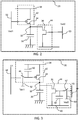
- Fig. 2 shows a first example of an actuator unit 20 as part of a device according to one or more of the claims.
- the actuation unit comprises an electroactive actuator 30 having at least two electrodes for driving the actuator.
- the actuator may be of the type of Figs. 1A or 1B or, alternatively, of another type of electroactive actuator.
- One electrode of the actuator 30 is connected to an electrical reference, which in this case is a ground terminal, and the other electrode is connected to a node 32.
- the node is at the junction between a first transistor 34 and a second transistor 36 which transistors are in series with each other between a first powerline 38 and a second power line 40.
- the power lines provide a source or sink of current for driving of the electroactive actuator. These are the lines that provide or sink the current for switching the electroactive actuator or for maintaining its state of actuation.
- the first transistor 34 is of p-type and the second transistor 36 is of n-type. This is advantageous with regard to the powerlines and some ways of addressing as described herein below. It is however not necessary and they may be of the same type.
- the first transistor channel is connected in series with the electroactive actuator between the first powerline 38 and the electrical reference while the second transistor channel is connected in series with the electroactive actuator between the second powerline 40 and the electrical reference.
- the first transistor 34 is part of a first circuit 42 including the transistor 34 for controlling current through the electroactive actuator 30 in a first direction (e.g. towards the electrical reference) in response to a first addressing signal Vad1 provided to the gate of the first transistor via a first addressing line 52 connected to the gate of the first transistor.
- the second transistor 36 is part of a second circuit 44 for controlling current through the electroactive actuator in a direction opposite to the first direction (e.g. away from the electrical reference) and in response to a second addressing signal Vad2 provided to the gate of the second transistor via a second addressing line 60 connected to the gate of the second transistor.
- first and second transistors enable to use the first and second transistors to control the drive current through the actuator with regard to its direction, magnitude and timing. Also, the combination of first and second circuits enables to select a charge (e.g. using the first circuit) or discharge (e.g. using the second circuit) mode which may be needed for actuators that work on the basis of charge and discharge.
- the first power line 38 can be at a voltage which is above the maximum voltage to be present at node 32 by a threshold amount and the second power line van be at a voltage which is below the minimum voltage to be present at node 32 by a threshold amount.
- the power line 38 can be at high voltage and the power line 40 a low voltage.
- the first and second power lines may for example be at +3V and -3V respectively, or at +5V and -5V respectively.
- the address lines carrying address signals Vad1 and Vad2 then have voltages of similar orders of magnitude to provide the required switching functionality. These values are given to show the order of magnitude, and to show the low voltage operation of ionic devices compared to high voltage field-driven devices.
- the actuator units of Fig 2 When multiple of the actuator units of Fig 2 are part of an array, they may share power lines 38 and 40. However, the address lines 52 and 60 need to be separate as otherwise driving of one actuator may influence another.
- Fig. 3 shows an actuator unit 30 which is a variation of the example of Fig. 2 . It has the advantage that not only powerlines may be shared between multiple actuator units, but also address lines can be shared. This reduces array complexity.
- the first circuit 42 also comprises a first switch 46 between a first data line 48 on which a voltage VI is provided and the gate of the first transistor 34.
- the circuit 42 also comprises a first capacitor 50 with one of its plates connected to the gate of the first transistor 34 between the gate and the first switch 46 and its other plate connected to the first power line 38 (this may be another electrical reference if needed).
- This capacitor can function as a storage capacitor for storing a voltage (in this case the data line voltage VI) provided to the gate of the first transistor.
- the capacitor 50 stores a gate-source voltage of the transistor 34.
- the first switch is controlled by a first addressing line 52 on which an address voltage Vad1 is provided.
- the second circuit 44 comprises a second switch 54 between a second data line 56 on which a voltage V2 is provided and the gate of the second transistor 36.
- the second circuit also comprises a storage capacitor 58 with one of its plates connected to the gate of the second transistor 36 between the gate and the second switch 54 and its other plate connected to the second power line 40 (this may be another electrical reference if needed). This capacitor can function for storing a voltage provided to the gate of the second transistor.
- the capacitor 58 stores the gate-source voltage of the transistor 36.
- the second switch is controlled by a second addressing line 60 on which a voltage Vad2 is provided.
- the switches 46, 54 for example comprise or consist of transistors, with the respective addressing lines 52 and 60 being connected to the transistor gates, and the source and drain connected to the respective data line and to the gate of the respective first/second transistor 34, 36.
- the first power line can be at a voltage which is above the maximum voltage to be present at node 32 by a threshold amount and the first power line is at a voltage which is below the minimum voltage to be present at node 32 by a threshold amount.
- the first and second power lines may be at +3V and -3V or +5V and -5V for example.
- the addressing lines carrying addressing signals Vad1 and Vad2 then have voltages of similar orders of magnitude to provide the required switching functionality.
- the data lines may be carrying voltages of the same magnitude. The sign of the voltages may depend on the types of transistors that are used for the first and second transistors. Those skilled in the art will be able to choose what voltages to apply for a type of transistor chosen. The above values are given simply to show the order of magnitude, and to show the low voltage operation of ionic devices compared to high voltage field-driven devices.
- the above described actuation units have drive units that makes use of two voltage driven sub-circuits.
- the first and second address lines 52, 60 comprise or consist of voltage supply conductors.
- the data lines 48 and 56 also comprise or consist of voltage supply conductors.
- Each transistor 34, 36 functions as a voltage to current converter, with its gate voltage determining the current flowing.
- these units may be called voltage addressed current driven units. While in the example of Fig. 2 it is the addressing voltages that determine the current flowing, in the example of Fig. 3 it is the data line voltages that define the flowing current.
- an electroactive actuator is associated with two addressing lines 52, 60, each line performing the dual role of selecting a unit and its mode of current flow during switching and or maintaining its actuation.
- the voltages as provided by the data lines to the gate of the transistors during an addressing period can be at least partly stored on the capacitors, the current flow in this unit can be maintained for at least some time even after the addressing signals have been removed. It is noted however, that the capacitors may be omitted as they are not necessary for a basic circuit having the switches 46 and 54.
- first and second circuits of Figs. 3 can be largely equivalent to that known active matrix circuits for driving an LED or OLED device.
- the transistor thus functions as a voltage controlled current source.
- the function of the storage capacitor is to help maintain a constant voltage at the control terminal of the current source in the period that the circuit is not being addressed.
- the first circuit can be used to cause the current-driven EAP to actuate in a given direction.
- the second circuit 44 is provided into the overall circuit.
- the second circuit is used to drive current in opposite direction through the electroactive actuator. It operates in the same way as the first circuit.
- the function of the storage capacitor is again to help maintain a constant voltage at the control terminal of the current source in the period that the circuit is not being addressed.
- the second circuit is used to cause the current driven actuator to actuate in the opposite direction to the first circuit.
- the above circuits or part of the circuits such as transistors may be built in technologies based on semiconductors such as amorphous silicon, low temperature laser crystallized Silicon (LTPS) or other amorphous semiconductors of which Zincoxide based semiconductors such as IndiumGalliumZincOxide (IGZO) are examples. These technologies are known from the display field. Alternatively, plastic electronics technologies may be used. These may be better compatible with electroactive actuators based on electroactive polymers.
- semiconductors such as amorphous silicon, low temperature laser crystallized Silicon (LTPS) or other amorphous semiconductors of which Zincoxide based semiconductors such as IndiumGalliumZincOxide (IGZO) are examples.
- LTPS low temperature laser crystallized Silicon
- IGZO Zincoxide based semiconductors
- IGZO IndiumGalliumZincOxide
- plastic electronics technologies may be used. These may be better compatible with electroactive actuators based on electroactive polymers.
- Fig. 4 shows how to combine the multiple ones (a plurality) of actuator units 30 of Fig. 3 into an array such as one of an active matrix array.
- Each actuator unit 60 is associated with two row addressing lines 52, 60 and two column data lines 48, 56.
- the first and second addressing lines 52, 60 for example comprise row conductors and the first and second data lines 48, 56 comprise column conductors.
- column and row are somewhat arbitrary.
- the addressing lines may comprise row lines while the data lines may comprise column lines.
- the first and second circuits each have a row (addressing) line and a column (data) line.
- the power lines may also be shared by different actuator units for example between those in rows and they thus can also be comprised in column lines. They have not been shown in Fig. 4 for clarity.
- the reference terminals of the actuator units may be common among many actuators in the array, for example all actuators in an addressing row or indeed all actuators in the array.
- actuator units 20 of Fig. 2 can also be combined in an array according to Fig.4 , such as an active matrix array, with the difference that now the data lines 48 and 56 of represent the addressing lines while the addressing lines 52 and 60 are omitted.
- the array is assumed to be initially in a specific actuated state and all rows are initially being supplied with a non-selection voltage (Vns). In this situation, no data can be transferred to the actuators.
- Vns non-selection voltage
- the first row of actuators is addressed with a selection voltage applied to both addressing lines 52, 60 and the other rows are not selected (Vns is still applied). If the actuator needs to be switched in one direction (can be charging of the actuator unit), a drive voltage VI is applied to the first data line 48 to produce the suitable current flowing into the actuator. If the actuator needs to be switched in the other direction (can be discharging of the actuator unit), a drive voltage V2 is applied to the second data line 56 to produce the suitable current flowing out from the actuator. At the end of this period a current will flow into or out from the actuators in the first row, and will be maintained by the storage capacitor.
- the second row of actuators is then addressed with a selection voltage applied to both addressing lines and the other rows are not selected (Vns). For each further row, the same process is then followed as for the preceding row until the full array has been addressed and actuated according to need.
- all rows can be deselected (with addressing voltage Vns) and voltages can be removed from the columns whereby the actuators will remain in their state of switching until the required end state of actuation is reached, at which point the array may be re-addressed to set only a sustain current (if required) in a manner similar to that described above.
- the sustain current is used to maintain an achieved state of actuation after a switching current has been provided.
- Fig. 5 shows a further example of an actuator unit 51 as part of a novel device.
- the actuation unit 51 of Fig. 5 comprises an electroactive actuator 30 with one electrode connected to a reference, such as ground, and the other electrode connected to a node 32.
- the node is at the junction between a first transistor 34 and a second transistor 36 between a first power line 38 and a second power line 40.
- the first transistor 34 is part of a first circuit 42 for controlling current through the electroactive actuator 30 in a first direction in response to a first addressing signal during a first addressing period.
- the second transistor 36 is part of a second circuit 44 for controlling a current through the electroactive polymer actuator in an opposite, second direction (e.g. away from ground) in response to a second addressing signal during a second addressing period.
- This unit differs from that in Figs. 2 or 3 in that it is provided with a data current I1 on a data line 70.
- the first circuit 42 comprises a first current mirror circuit formed in part by the first transistor 34 and a reference transistor 72.
- the data current I1 is provided through the reference transistor 72, and it is mirrored by a first mirror transistor 74 and again by another current mirror circuit formed by the combination of a second mirror transistor 76 and the first transistor 34.
- the first circuit 44 comprises a second current mirror circuit formed by the second transistor 36 and the reference transistor 72.
- a first switch 78 is between the data line 70 and the reference transistor 72 and it is controlled by a first addressing line 80 on which a voltage Vad1 is provided.
- a selection circuit is also provided which comprises a further first switch 84 for interrupting the current flow through the first current mirror and a further second switch 86 for interrupting the current flow through the second current mirror circuit.
- a selection line 82 is provided for carrying a selection voltage Vsel for controlling the further first and second switches. The selection line and voltage thereon can thus be used to control two series switches 84, 86 in complementary manner. The selection circuit is thus for selecting the first or second current mirror for mirroring the current sampled from the data line 70 under control of the second addressing line 82.
- the first addressing line 80, the data line 70 and second addressing line 82 may each comprise a separate conductor.
- the conductor 82 selects a direction of current flow (which may be charging or discharging of an actuator) and the other column conductor 70 provides the current to be mirrored.
- each actuator unit needs only three conductors. In this case, the mode selection and actuator selection are separated, but the two functions are again achieved with two addressing lines.
- the first circuit may comprise a storage capacitor 88 for storing a voltage on the gate of the reference transistor 72 in response to a current provided from the data line 70.
- This provides a current sample and hold function which is shared between the first and second circuits.
- Capacitor 88 stores the gate voltage for transistors 36 and 74 and transistor 74 enables the current to be copied into transistor 34 and hence into actuator 30. Having one current driver via data line 70 in the peripheral circuitry is easier to deal with and cheaper than having two with opposite polarities.
- the capacitor 88 can be devided in two, one still as capacitor 88 and a new capacitor at the gate of transistor 34. This would need another switch to address it with a voltage, much like in the Fig. 3 circuit. Alternatively the address circuitry on right of the Fig. 5 and implement that for transistor 34 so that transistor 34 can be addressed using current copy i.e. as transistor 36 is addressed. A power save can be realized by adding in a switch and capacitor at the gate of transistor 34, and this would be advantageous, but extra switches would be required to shut the current path between transistors 74 and 76 given that 84 will be closed.
- the voltages chosen for the circuit of Fig. 5 will be suitable for the technology used, such as LTPS or types of technology as described hereinabove.
- the currents chosen will be suitable for the particular type of electroactive actuator.
- Fig. 6 shows how to combine multiple ones of the actuator unit 51 of Fig. 5 into an array such as an active matrix array.
- Each unit 51 is associated with one row addressing line and two column lines, one of which is an addressing line and one which is a data line.
- the first addressing line 80 may comprise a row conductor and the data line 70 and second addressing line 82 each comprise a column conductor. This may however also be reversed in that the addressing line may comprise or consist of a column conductor while the data line and second addressing line comprise or consist of row conductors.
- the first row of actuators is addressed with a selection voltage applied to the addressing line 80 and the other rows are not selected (Vns is still applied).
- a current direction mode (can be charge or discharge mode) is selected using the second addressing line 82.
- the desired current is applied to the data line 70 from a current driver.
- the second row of actuators is then addressed with a selection voltage applied to the row addressing line and the other rows are not selected (Vns). The same process is then followed as for the preceding row.
- all rows can be deselected (with addressing voltage Vns).
- the array may be periodically re-addressed to provide only a sustain current if required.
- a sustain current may be needed to maintain a desired actuation state. This may be achieved by periodically re-addressing the array with a suitable current level. Most of the time, the actuators in the array may be in this sustain mode, and it is therefore important that the sustain current can be accurately set at a level required for the state of actuation and maintained.
- the sustain currents required are characteristic of the particular electroactive actuator and may even depend on the actuation state. They may be defined in a look up table either provided by the manufacturer or obtained during a product calibration and testing phase.
- Fig. 7 shows an actuator unit 71 which is a modification of the actuator unit of Fig. 3 for enabling a high level drive current and a low level sustain current. Delivery of both currents typically is difficult with one type of transistor.
- the first circuit comprises a first boost transistor 34' which is connected in parallel with the first transistor 34 between the first power line 38 and the node 32.
- the gates of the first transistor and the first boost transistor are connected.
- the first circuit also comprises a further first switch 92 for enabling or disabling the current path the first boost transistor provides.
- the switch 92 is between the powerline 38 and the first boost transistor. It may however also be provided between the gates of the first transistor and the first boost transistor.
- the second circuit comprises a second boost transistor 36' which is connected parallel with the second transistor 36, between the second power line 40 and the node 32 with its gate connected to that of the second transistor 36.
- the second circuit also comprises a further second switch 94 for enabling or disabling the current path the second boost transistor provides.
- the switch 94 is between the powerline 40 and the second boost transistor. It may however also be provided between the gates of the second transistor and the second boost transistor.
- An enable line 90 is provided connecting to the further first and second switches 92 and 94, for enabling or disabling the boost transistors using an enable signal Ven.
- a parallel boost transistor when activated means that two currents flow in parallel into or out of the actuator. As a result a higher current is realized. Such a higher current can advantageously be used for the switching current required to change the actuation state of the actuator.
- the boost transistor is designed to provide a larger current than the first/second transistor so that the switching current can become much larger. For example, if the boost transistor is five times the size of the first/second transistor, the sum will be six times the current of the first/second transistor only.
- the most straightforward method of designing a higher current output is by dimensioning the transistor to have a higher width to length ratio which is a matter of layout design.
- Clearly alternative approaches may be used to adjust any of the other factors in the above transistor current equations.
- If an accurate sustain current is needed after switching the smaller one of the parallel transistors may be used while the boost transistor is disabled using the enable/disable signal.
- Fig. 8 shows how the additional boost transistors alter the matrix design of Fig.5 . It shows that the enable line 90 is provided as an additional row conductor.
- the enable line is used to provide both parallel transistors in the circuit.
- a periodic readdressing may be performed with the boost transistors disabled, so that a sustain current level is supplied to (or drained from) the actuators using the first or second transistors.
- Fig. 9 shows a method of actuating a device which comprises an active matrix array of electroactive actuators.
- the method comprises, in step 100, using a set of addressing lines to select a group of electroactive actuators in a first direction current mode (this may be a discharge or charge mode) during different addressing periods.
- a first direction current mode this may be a discharge or charge mode
- step 102 comprises using a first circuit to drive a controllable current through the electroactive actuator in a first direction in response to a first addressing signal.
- step 104 comprises using a second circuit to drive a controllable current through the electroactive actuator in an opposite, second direction in response to a second addressing signal.
- the electroactive actuator comprises an electroactive material structure for providing a mechanical actuation such that the structure defines a non-actuated state and at least one actuated state (different from the non-actuated state) attainable by application of an electrical drive current to the structure.
- the actuator has an electrode arrangement having at least two electrodes for providing the drive current to the material.
- each unit may be sandwiched between the electrodes.
- electrodes can be on a same side of the material. In either case, electrodes can be physically attached to the material either directly without any (passive) layers in between, or indirectly with additional (passive) layers in between.
- the electrodes may be stretchable so that they follow the deformation of the electroactive actuator.
- Materials suitable for the electrodes are also known, and may for example be selected from the group consisting of thin metal films, such as gold, copper, or aluminum or organic conductors such as carbon black, carbon nanotubes, graphene, poly-aniline (PANI), poly(3,4-ethylenedioxythiophene) (PEDOT), e.g.
- PET poly(3,4-ethylenedioxythiophene) poly(styrenesulfonate)
- Metalized polyester films may also be used, such as metalized polyethylene terephthalate (PET), for example using an aluminum coating.
- the materials for the different layers will be selected for example taking account of the elastic moduli (Young's moduli) of the different layers.
- a 2x2 array has been shown in the Figs.
- n ⁇ 2 and m ⁇ 2 for example n ⁇ 4 or n ⁇ 10 or n ⁇ 50 and/or m ⁇ 4 or m ⁇ 10 or m ⁇ 50.
- the circuits above are based on the use of transistors, and the switches may also be transistors.
- the transistors are preferably made as thin film transistors in for example amorphous silicon or IGZO or polysilicon technology.
- Electroactive actuators Materials suitable for the electroactive actuators are known. They may be of inorganic nature or of organic nature. Preferably they are of organic nature as this provides facile design options.
- the electroactive materials preferably are of the polymeric type so that the electroactive actuators are electroactive polymer actuators.
- Electroactive polymers include, but are not limited to, the sub-classes: piezoelectric polymers, electromechanical polymers, relaxor ferroelectric polymers, electrostrictive polymers, dielectric elastomers, liquid crystal elastomers, conjugated polymers, Ionic Polymer Metal Composites, ionic gels and polymer gels.
- Ionic EAPs which are the subject of this invention are activated by an electrically induced transport of ions and/or solvent within a transport medium. They usually require low voltages but high currents.
- the medium may comprise a liquid/gel electrolyte medium (although some material systems can also operate using solid electrolytes in the form of e.g. polyemers).
- These devices may operate with a large hysteresis loop.
- a large injection of current is needed to move around the hysteresis loop and thus change the actuation state, and a small sustain current is needed to retain a level of actuation.
- the sustain current may also be needed.
- IPMCs Ionic Polymer Metal Composites
- Typical electrode materials are Pt, Gd, CNTs, CPs, Pd.
- Typical electrolytes are Li+ and Na+ water-based solutions.
- cations typically travel to the cathode side together with water. This leads to reorganization of hydrophilic clusters and to polymer expansion. Strain in the cathode area leads to stress in rest of the polymer matrix resulting in bending towards the anode. Reversing the applied voltage inverts bending.
- Well known polymer membranes are Nafion® and Flemion®.
- conjugated/conducting polymers Another notable subclass of Ionic polymers is conjugated/conducting polymers.
- a conjugated polymer actuator typically consists of an electrolyte sandwiched by two layers of the conjugated polymer. The electrolyte is used to change oxidation state. When a potential is applied to the polymer through the electrolyte, electrons are added to or removed from the polymer, driving oxidation and reduction. Reduction results in contraction, oxidation in expansion.
- the electrolyte can be a liquid, a gel or a solid material (i.e. complex of high molecular weight polymers and metal salts).
- Most common conjugated polymers are polypyrrole (PPy), Polyaniline (PANi) and polythiophene (PTh).
- the strain induced in the device is for example proportional to charge (and hence the strain rate is proportional to current). This is for example the case for polypyrrole. This linear relationship between strain and charge is valid over a large frequency range up to 1Hz.
- a simple model representing the electrical behavior is a large capacitor with a parallel resistor, in series with another resistor.
- the imposed voltage can induce all kinds of deformations such as twisting, rolling, torsioning, turning, and non-symmetric bending deformation.
- actuators and especially the ones of organic type provide unique benefits mainly because of the small form factor, the flexibility and the high energy density. Hence they can be easily integrated in soft, 3D-shaped and / or miniature products and interfaces. Examples of such applications are:
- Optical elements such as lenses, reflective surfaces, gratings etc. can be made adaptive by shape or position adaptation using actuators.
- the benefits of actuators are for example the lower power consumption.
- row and column are somewhat arbitrary and are merely used to denote orthogonal lines. Thus, while a row is generally considered to run from left to right and a column is generally considered to run from top to bottom, this does not exclude that a row may run up and down and a column run left to right if a device is rotationally oriented in a particular way. Thus “row” and “column” are merely used for ease of the reader and could be considered equivalent to "a first vector direction” and "a second, orthogonal, vector direction”.
- the device as defined by the claims comprises electroactive polymer actuators each of which is addressed by two addressing lines for selecting the electroactive polymer actuator and a current direction drive mode.
- a first circuit is for driving a controllable current through the electroactive actuator in a first direction and a second circuit is for driving a controllable current through the electroactive actuator in a second direction, opposite to the first direction.
Landscapes
- Physics & Mathematics (AREA)
- Spectroscopy & Molecular Physics (AREA)
- Control Of Indicators Other Than Cathode Ray Tubes (AREA)
Priority Applications (6)
| Application Number | Priority Date | Filing Date | Title |
|---|---|---|---|
| EP18156078.0A EP3525251A1 (de) | 2018-02-09 | 2018-02-09 | Aktuatorvorrichtung mit stromadressiertem elektroaktivem polymer |
| CN201980011745.9A CN111684613A (zh) | 2018-02-09 | 2019-01-29 | 使用电流寻址的电活性聚合物的致动器设备 |
| JP2020542640A JP2021513742A (ja) | 2018-02-09 | 2019-01-29 | 電流アドレッシング型電気活性高分子を使用するアクチュエータデバイス |
| EP19701364.2A EP3750197B1 (de) | 2018-02-09 | 2019-01-29 | Aktuatorvorrichtung mit stromadressiertem elektroaktivem polymer |
| US16/968,617 US20210050505A1 (en) | 2018-02-09 | 2019-01-29 | Actuator device using current-addressed electroactive polymer |
| PCT/EP2019/052032 WO2019154664A1 (en) | 2018-02-09 | 2019-01-29 | Actuator device using current-addressed electroactive polymer |
Applications Claiming Priority (1)
| Application Number | Priority Date | Filing Date | Title |
|---|---|---|---|
| EP18156078.0A EP3525251A1 (de) | 2018-02-09 | 2018-02-09 | Aktuatorvorrichtung mit stromadressiertem elektroaktivem polymer |
Publications (1)
| Publication Number | Publication Date |
|---|---|
| EP3525251A1 true EP3525251A1 (de) | 2019-08-14 |
Family
ID=61192726
Family Applications (2)
| Application Number | Title | Priority Date | Filing Date |
|---|---|---|---|
| EP18156078.0A Withdrawn EP3525251A1 (de) | 2018-02-09 | 2018-02-09 | Aktuatorvorrichtung mit stromadressiertem elektroaktivem polymer |
| EP19701364.2A Not-in-force EP3750197B1 (de) | 2018-02-09 | 2019-01-29 | Aktuatorvorrichtung mit stromadressiertem elektroaktivem polymer |
Family Applications After (1)
| Application Number | Title | Priority Date | Filing Date |
|---|---|---|---|
| EP19701364.2A Not-in-force EP3750197B1 (de) | 2018-02-09 | 2019-01-29 | Aktuatorvorrichtung mit stromadressiertem elektroaktivem polymer |
Country Status (5)
| Country | Link |
|---|---|
| US (1) | US20210050505A1 (de) |
| EP (2) | EP3525251A1 (de) |
| JP (1) | JP2021513742A (de) |
| CN (1) | CN111684613A (de) |
| WO (1) | WO2019154664A1 (de) |
Families Citing this family (1)
| Publication number | Priority date | Publication date | Assignee | Title |
|---|---|---|---|---|
| CN110214381B (zh) * | 2017-01-23 | 2023-04-18 | 皇家飞利浦有限公司 | 基于电活性材料的致动器设备 |
Citations (4)
| Publication number | Priority date | Publication date | Assignee | Title |
|---|---|---|---|---|
| WO2014045605A1 (ja) * | 2012-09-24 | 2014-03-27 | パナソニック株式会社 | 表示装置 |
| JP2015204702A (ja) * | 2014-04-15 | 2015-11-16 | セイコーエプソン株式会社 | アクチュエーター装置、触覚ディスプレイおよび駆動方法 |
| WO2017108443A1 (en) | 2015-12-21 | 2017-06-29 | Koninklijke Philips N.V. | Actuator device based on an electroactive polymer |
| WO2017108489A1 (en) | 2015-12-21 | 2017-06-29 | Koninklijke Philips N.V. | Actuator device based on an electroactive polymer |
Family Cites Families (16)
| Publication number | Priority date | Publication date | Assignee | Title |
|---|---|---|---|---|
| US3623033A (en) * | 1970-06-29 | 1971-11-23 | Electronic Memories & Magnetic | Cross-coupled bridge core memory addressing system |
| US4523302A (en) * | 1981-07-16 | 1985-06-11 | Ampex Corporation | Core memory with return drive scheme |
| JP2689916B2 (ja) * | 1994-08-09 | 1997-12-10 | 日本電気株式会社 | アクティブマトリクス型電流制御型発光素子の駆動回路 |
| JP3116886B2 (ja) * | 1998-01-16 | 2000-12-11 | 日本電気株式会社 | ピエゾ駆動回路 |
| DE60011038T2 (de) * | 2000-04-01 | 2005-07-21 | Robert Bosch Gmbh | Zeit und Fall-kontrolliertes Aktivierungssystem für die Aufladung und die Entladung von piezoelektrischen Elementen |
| JP2002351401A (ja) * | 2001-03-21 | 2002-12-06 | Mitsubishi Electric Corp | 自発光型表示装置 |
| JP2003052181A (ja) * | 2001-05-29 | 2003-02-21 | Olympus Optical Co Ltd | 圧電アクチュエータとその駆動装置及び圧電アクチュエータを用いた可変ミラーを有するカメラ |
| JP4650601B2 (ja) * | 2001-09-05 | 2011-03-16 | 日本電気株式会社 | 電流駆動素子の駆動回路及び駆動方法ならびに画像表示装置 |
| JP3842665B2 (ja) * | 2002-02-15 | 2006-11-08 | 株式会社日本自動車部品総合研究所 | ピエゾアクチュエータ制御装置およびそれを用いた燃料噴射制御システム |
| US20070040471A1 (en) * | 2005-08-17 | 2007-02-22 | Nokia Corporation | Load adaptive class de driving amplifier for piezoelectric actuators |
| JP2008089572A (ja) * | 2006-09-08 | 2008-04-17 | Seiko Epson Corp | 駆動装置、物理量測定装置及び電子機器 |
| JP2008287140A (ja) * | 2007-05-21 | 2008-11-27 | Sony Corp | 表示装置及び電子機器 |
| US8427115B2 (en) * | 2008-07-08 | 2013-04-23 | Toshiba Tec Kabushiki Kaisha | Driving device for capacitance type actuator and driving device for ink jet head |
| JP5305242B2 (ja) * | 2009-06-09 | 2013-10-02 | カシオ計算機株式会社 | 画素駆動回路、発光装置及びその駆動制御方法、並びに電子機器 |
| WO2015045605A1 (ja) * | 2013-09-27 | 2015-04-02 | カシオ計算機株式会社 | 駆動素子及び駆動素子の駆動方法 |
| RU2723887C2 (ru) * | 2015-08-31 | 2020-06-18 | Конинклейке Филипс Н.В. | Датчики на основе электроактивных полимеров и способы восприятия |
-
2018
- 2018-02-09 EP EP18156078.0A patent/EP3525251A1/de not_active Withdrawn
-
2019
- 2019-01-29 CN CN201980011745.9A patent/CN111684613A/zh active Pending
- 2019-01-29 EP EP19701364.2A patent/EP3750197B1/de not_active Not-in-force
- 2019-01-29 WO PCT/EP2019/052032 patent/WO2019154664A1/en not_active Ceased
- 2019-01-29 JP JP2020542640A patent/JP2021513742A/ja active Pending
- 2019-01-29 US US16/968,617 patent/US20210050505A1/en not_active Abandoned
Patent Citations (4)
| Publication number | Priority date | Publication date | Assignee | Title |
|---|---|---|---|---|
| WO2014045605A1 (ja) * | 2012-09-24 | 2014-03-27 | パナソニック株式会社 | 表示装置 |
| JP2015204702A (ja) * | 2014-04-15 | 2015-11-16 | セイコーエプソン株式会社 | アクチュエーター装置、触覚ディスプレイおよび駆動方法 |
| WO2017108443A1 (en) | 2015-12-21 | 2017-06-29 | Koninklijke Philips N.V. | Actuator device based on an electroactive polymer |
| WO2017108489A1 (en) | 2015-12-21 | 2017-06-29 | Koninklijke Philips N.V. | Actuator device based on an electroactive polymer |
Also Published As
| Publication number | Publication date |
|---|---|
| EP3750197A1 (de) | 2020-12-16 |
| EP3750197B1 (de) | 2021-09-15 |
| US20210050505A1 (en) | 2021-02-18 |
| WO2019154664A1 (en) | 2019-08-15 |
| CN111684613A (zh) | 2020-09-18 |
| JP2021513742A (ja) | 2021-05-27 |
Similar Documents
| Publication | Publication Date | Title |
|---|---|---|
| EP3394909B1 (de) | Aktuatorvorrichtung auf basis eines elektroaktiven polymers | |
| EP3304608B1 (de) | Betätigungsvorrichtung | |
| US20190237651A1 (en) | Eap actuator and drive method | |
| EP3750197B1 (de) | Aktuatorvorrichtung mit stromadressiertem elektroaktivem polymer | |
| US11139426B2 (en) | Actuator device based on an electroactive polymer | |
| EP3523832B1 (de) | Aktuatorvorrichtung auf basis eines elektroaktiven polymers | |
| CN110214381B (zh) | 基于电活性材料的致动器设备 | |
| JP2015204702A (ja) | アクチュエーター装置、触覚ディスプレイおよび駆動方法 | |
| JP2015169815A (ja) | アクチュエーター装置、触覚ディスプレイおよび駆動方法 | |
| EP3479419B1 (de) | Eap-aktor und ansteuerungsverfahren | |
| JP2015156775A (ja) | アクチュエーター装置、触覚ディスプレイおよび駆動方法 |
Legal Events
| Date | Code | Title | Description |
|---|---|---|---|
| PUAI | Public reference made under article 153(3) epc to a published international application that has entered the european phase |
Free format text: ORIGINAL CODE: 0009012 |
|
| AK | Designated contracting states |
Kind code of ref document: A1 Designated state(s): AL AT BE BG CH CY CZ DE DK EE ES FI FR GB GR HR HU IE IS IT LI LT LU LV MC MK MT NL NO PL PT RO RS SE SI SK SM TR |
|
| AX | Request for extension of the european patent |
Extension state: BA ME |
|
| RAP1 | Party data changed (applicant data changed or rights of an application transferred) |
Owner name: KONINKLIJKE PHILIPS N.V. |
|
| STAA | Information on the status of an ep patent application or granted ep patent |
Free format text: STATUS: THE APPLICATION IS DEEMED TO BE WITHDRAWN |
|
| 18D | Application deemed to be withdrawn |
Effective date: 20200215 |