EP3525254A2 - Afficheur - Google Patents
Afficheur Download PDFInfo
- Publication number
- EP3525254A2 EP3525254A2 EP19152453.7A EP19152453A EP3525254A2 EP 3525254 A2 EP3525254 A2 EP 3525254A2 EP 19152453 A EP19152453 A EP 19152453A EP 3525254 A2 EP3525254 A2 EP 3525254A2
- Authority
- EP
- European Patent Office
- Prior art keywords
- power supply
- supply line
- insulating layer
- driving circuit
- display device
- Prior art date
- Legal status (The legal status is an assumption and is not a legal conclusion. Google has not performed a legal analysis and makes no representation as to the accuracy of the status listed.)
- Granted
Links
Images


Classifications
-
- H—ELECTRICITY
- H10—SEMICONDUCTOR DEVICES; ELECTRIC SOLID-STATE DEVICES NOT OTHERWISE PROVIDED FOR
- H10D—INORGANIC ELECTRIC SEMICONDUCTOR DEVICES
- H10D86/00—Integrated devices formed in or on insulating or conducting substrates, e.g. formed in silicon-on-insulator [SOI] substrates or on stainless steel or glass substrates
- H10D86/40—Integrated devices formed in or on insulating or conducting substrates, e.g. formed in silicon-on-insulator [SOI] substrates or on stainless steel or glass substrates characterised by multiple TFTs
- H10D86/441—Interconnections, e.g. scanning lines
-
- H—ELECTRICITY
- H10—SEMICONDUCTOR DEVICES; ELECTRIC SOLID-STATE DEVICES NOT OTHERWISE PROVIDED FOR
- H10K—ORGANIC ELECTRIC SOLID-STATE DEVICES
- H10K59/00—Integrated devices, or assemblies of multiple devices, comprising at least one organic light-emitting element covered by group H10K50/00
- H10K59/10—OLED displays
- H10K59/12—Active-matrix OLED [AMOLED] displays
- H10K59/121—Active-matrix OLED [AMOLED] displays characterised by the geometry or disposition of pixel elements
-
- G—PHYSICS
- G09—EDUCATION; CRYPTOGRAPHY; DISPLAY; ADVERTISING; SEALS
- G09G—ARRANGEMENTS OR CIRCUITS FOR CONTROL OF INDICATING DEVICES USING STATIC MEANS TO PRESENT VARIABLE INFORMATION
- G09G3/00—Control arrangements or circuits, of interest only in connection with visual indicators other than cathode-ray tubes
- G09G3/20—Control arrangements or circuits, of interest only in connection with visual indicators other than cathode-ray tubes for presentation of an assembly of a number of characters, e.g. a page, by composing the assembly by combination of individual elements arranged in a matrix no fixed position being assigned to or needed to be assigned to the individual characters or partial characters
- G09G3/22—Control arrangements or circuits, of interest only in connection with visual indicators other than cathode-ray tubes for presentation of an assembly of a number of characters, e.g. a page, by composing the assembly by combination of individual elements arranged in a matrix no fixed position being assigned to or needed to be assigned to the individual characters or partial characters using controlled light sources
- G09G3/30—Control arrangements or circuits, of interest only in connection with visual indicators other than cathode-ray tubes for presentation of an assembly of a number of characters, e.g. a page, by composing the assembly by combination of individual elements arranged in a matrix no fixed position being assigned to or needed to be assigned to the individual characters or partial characters using controlled light sources using electroluminescent panels
- G09G3/32—Control arrangements or circuits, of interest only in connection with visual indicators other than cathode-ray tubes for presentation of an assembly of a number of characters, e.g. a page, by composing the assembly by combination of individual elements arranged in a matrix no fixed position being assigned to or needed to be assigned to the individual characters or partial characters using controlled light sources using electroluminescent panels semiconductive, e.g. using light-emitting diodes [LED]
- G09G3/3208—Control arrangements or circuits, of interest only in connection with visual indicators other than cathode-ray tubes for presentation of an assembly of a number of characters, e.g. a page, by composing the assembly by combination of individual elements arranged in a matrix no fixed position being assigned to or needed to be assigned to the individual characters or partial characters using controlled light sources using electroluminescent panels semiconductive, e.g. using light-emitting diodes [LED] organic, e.g. using organic light-emitting diodes [OLED]
- G09G3/3225—Control arrangements or circuits, of interest only in connection with visual indicators other than cathode-ray tubes for presentation of an assembly of a number of characters, e.g. a page, by composing the assembly by combination of individual elements arranged in a matrix no fixed position being assigned to or needed to be assigned to the individual characters or partial characters using controlled light sources using electroluminescent panels semiconductive, e.g. using light-emitting diodes [LED] organic, e.g. using organic light-emitting diodes [OLED] using an active matrix
- G09G3/3233—Control arrangements or circuits, of interest only in connection with visual indicators other than cathode-ray tubes for presentation of an assembly of a number of characters, e.g. a page, by composing the assembly by combination of individual elements arranged in a matrix no fixed position being assigned to or needed to be assigned to the individual characters or partial characters using controlled light sources using electroluminescent panels semiconductive, e.g. using light-emitting diodes [LED] organic, e.g. using organic light-emitting diodes [OLED] using an active matrix with pixel circuitry controlling the current through the light-emitting element
-
- G—PHYSICS
- G09—EDUCATION; CRYPTOGRAPHY; DISPLAY; ADVERTISING; SEALS
- G09G—ARRANGEMENTS OR CIRCUITS FOR CONTROL OF INDICATING DEVICES USING STATIC MEANS TO PRESENT VARIABLE INFORMATION
- G09G3/00—Control arrangements or circuits, of interest only in connection with visual indicators other than cathode-ray tubes
- G09G3/20—Control arrangements or circuits, of interest only in connection with visual indicators other than cathode-ray tubes for presentation of an assembly of a number of characters, e.g. a page, by composing the assembly by combination of individual elements arranged in a matrix no fixed position being assigned to or needed to be assigned to the individual characters or partial characters
- G09G3/22—Control arrangements or circuits, of interest only in connection with visual indicators other than cathode-ray tubes for presentation of an assembly of a number of characters, e.g. a page, by composing the assembly by combination of individual elements arranged in a matrix no fixed position being assigned to or needed to be assigned to the individual characters or partial characters using controlled light sources
- G09G3/30—Control arrangements or circuits, of interest only in connection with visual indicators other than cathode-ray tubes for presentation of an assembly of a number of characters, e.g. a page, by composing the assembly by combination of individual elements arranged in a matrix no fixed position being assigned to or needed to be assigned to the individual characters or partial characters using controlled light sources using electroluminescent panels
- G09G3/32—Control arrangements or circuits, of interest only in connection with visual indicators other than cathode-ray tubes for presentation of an assembly of a number of characters, e.g. a page, by composing the assembly by combination of individual elements arranged in a matrix no fixed position being assigned to or needed to be assigned to the individual characters or partial characters using controlled light sources using electroluminescent panels semiconductive, e.g. using light-emitting diodes [LED]
- G09G3/3208—Control arrangements or circuits, of interest only in connection with visual indicators other than cathode-ray tubes for presentation of an assembly of a number of characters, e.g. a page, by composing the assembly by combination of individual elements arranged in a matrix no fixed position being assigned to or needed to be assigned to the individual characters or partial characters using controlled light sources using electroluminescent panels semiconductive, e.g. using light-emitting diodes [LED] organic, e.g. using organic light-emitting diodes [OLED]
- G09G3/3266—Details of drivers for scan electrodes
-
- G—PHYSICS
- G09—EDUCATION; CRYPTOGRAPHY; DISPLAY; ADVERTISING; SEALS
- G09G—ARRANGEMENTS OR CIRCUITS FOR CONTROL OF INDICATING DEVICES USING STATIC MEANS TO PRESENT VARIABLE INFORMATION
- G09G3/00—Control arrangements or circuits, of interest only in connection with visual indicators other than cathode-ray tubes
- G09G3/20—Control arrangements or circuits, of interest only in connection with visual indicators other than cathode-ray tubes for presentation of an assembly of a number of characters, e.g. a page, by composing the assembly by combination of individual elements arranged in a matrix no fixed position being assigned to or needed to be assigned to the individual characters or partial characters
- G09G3/22—Control arrangements or circuits, of interest only in connection with visual indicators other than cathode-ray tubes for presentation of an assembly of a number of characters, e.g. a page, by composing the assembly by combination of individual elements arranged in a matrix no fixed position being assigned to or needed to be assigned to the individual characters or partial characters using controlled light sources
- G09G3/30—Control arrangements or circuits, of interest only in connection with visual indicators other than cathode-ray tubes for presentation of an assembly of a number of characters, e.g. a page, by composing the assembly by combination of individual elements arranged in a matrix no fixed position being assigned to or needed to be assigned to the individual characters or partial characters using controlled light sources using electroluminescent panels
- G09G3/32—Control arrangements or circuits, of interest only in connection with visual indicators other than cathode-ray tubes for presentation of an assembly of a number of characters, e.g. a page, by composing the assembly by combination of individual elements arranged in a matrix no fixed position being assigned to or needed to be assigned to the individual characters or partial characters using controlled light sources using electroluminescent panels semiconductive, e.g. using light-emitting diodes [LED]
- G09G3/3208—Control arrangements or circuits, of interest only in connection with visual indicators other than cathode-ray tubes for presentation of an assembly of a number of characters, e.g. a page, by composing the assembly by combination of individual elements arranged in a matrix no fixed position being assigned to or needed to be assigned to the individual characters or partial characters using controlled light sources using electroluminescent panels semiconductive, e.g. using light-emitting diodes [LED] organic, e.g. using organic light-emitting diodes [OLED]
- G09G3/3275—Details of drivers for data electrodes
-
- H—ELECTRICITY
- H05—ELECTRIC TECHNIQUES NOT OTHERWISE PROVIDED FOR
- H05K—PRINTED CIRCUITS; CASINGS OR CONSTRUCTIONAL DETAILS OF ELECTRIC APPARATUS; MANUFACTURE OF ASSEMBLAGES OF ELECTRICAL COMPONENTS
- H05K1/00—Printed circuits
- H05K1/18—Printed circuits structurally associated with non-printed electric components
- H05K1/189—Printed circuits structurally associated with non-printed electric components characterised by the use of flexible or folded printed circuits
-
- H—ELECTRICITY
- H10—SEMICONDUCTOR DEVICES; ELECTRIC SOLID-STATE DEVICES NOT OTHERWISE PROVIDED FOR
- H10D—INORGANIC ELECTRIC SEMICONDUCTOR DEVICES
- H10D86/00—Integrated devices formed in or on insulating or conducting substrates, e.g. formed in silicon-on-insulator [SOI] substrates or on stainless steel or glass substrates
- H10D86/40—Integrated devices formed in or on insulating or conducting substrates, e.g. formed in silicon-on-insulator [SOI] substrates or on stainless steel or glass substrates characterised by multiple TFTs
- H10D86/451—Integrated devices formed in or on insulating or conducting substrates, e.g. formed in silicon-on-insulator [SOI] substrates or on stainless steel or glass substrates characterised by multiple TFTs characterised by the compositions or shapes of the interlayer dielectrics
-
- H—ELECTRICITY
- H10—SEMICONDUCTOR DEVICES; ELECTRIC SOLID-STATE DEVICES NOT OTHERWISE PROVIDED FOR
- H10D—INORGANIC ELECTRIC SEMICONDUCTOR DEVICES
- H10D86/00—Integrated devices formed in or on insulating or conducting substrates, e.g. formed in silicon-on-insulator [SOI] substrates or on stainless steel or glass substrates
- H10D86/40—Integrated devices formed in or on insulating or conducting substrates, e.g. formed in silicon-on-insulator [SOI] substrates or on stainless steel or glass substrates characterised by multiple TFTs
- H10D86/60—Integrated devices formed in or on insulating or conducting substrates, e.g. formed in silicon-on-insulator [SOI] substrates or on stainless steel or glass substrates characterised by multiple TFTs wherein the TFTs are in active matrices
-
- H—ELECTRICITY
- H10—SEMICONDUCTOR DEVICES; ELECTRIC SOLID-STATE DEVICES NOT OTHERWISE PROVIDED FOR
- H10K—ORGANIC ELECTRIC SOLID-STATE DEVICES
- H10K50/00—Organic light-emitting devices
- H10K50/80—Constructional details
- H10K50/805—Electrodes
- H10K50/81—Anodes
-
- H—ELECTRICITY
- H10—SEMICONDUCTOR DEVICES; ELECTRIC SOLID-STATE DEVICES NOT OTHERWISE PROVIDED FOR
- H10K—ORGANIC ELECTRIC SOLID-STATE DEVICES
- H10K50/00—Organic light-emitting devices
- H10K50/80—Constructional details
- H10K50/805—Electrodes
- H10K50/82—Cathodes
-
- H—ELECTRICITY
- H10—SEMICONDUCTOR DEVICES; ELECTRIC SOLID-STATE DEVICES NOT OTHERWISE PROVIDED FOR
- H10K—ORGANIC ELECTRIC SOLID-STATE DEVICES
- H10K50/00—Organic light-emitting devices
- H10K50/80—Constructional details
- H10K50/84—Passivation; Containers; Encapsulations
- H10K50/842—Containers
- H10K50/8426—Peripheral sealing arrangements, e.g. adhesives, sealants
-
- H—ELECTRICITY
- H10—SEMICONDUCTOR DEVICES; ELECTRIC SOLID-STATE DEVICES NOT OTHERWISE PROVIDED FOR
- H10K—ORGANIC ELECTRIC SOLID-STATE DEVICES
- H10K59/00—Integrated devices, or assemblies of multiple devices, comprising at least one organic light-emitting element covered by group H10K50/00
- H10K59/10—OLED displays
- H10K59/12—Active-matrix OLED [AMOLED] displays
- H10K59/121—Active-matrix OLED [AMOLED] displays characterised by the geometry or disposition of pixel elements
- H10K59/1213—Active-matrix OLED [AMOLED] displays characterised by the geometry or disposition of pixel elements the pixel elements being TFTs
-
- H—ELECTRICITY
- H10—SEMICONDUCTOR DEVICES; ELECTRIC SOLID-STATE DEVICES NOT OTHERWISE PROVIDED FOR
- H10K—ORGANIC ELECTRIC SOLID-STATE DEVICES
- H10K59/00—Integrated devices, or assemblies of multiple devices, comprising at least one organic light-emitting element covered by group H10K50/00
- H10K59/10—OLED displays
- H10K59/12—Active-matrix OLED [AMOLED] displays
- H10K59/121—Active-matrix OLED [AMOLED] displays characterised by the geometry or disposition of pixel elements
- H10K59/1216—Active-matrix OLED [AMOLED] displays characterised by the geometry or disposition of pixel elements the pixel elements being capacitors
-
- H—ELECTRICITY
- H10—SEMICONDUCTOR DEVICES; ELECTRIC SOLID-STATE DEVICES NOT OTHERWISE PROVIDED FOR
- H10K—ORGANIC ELECTRIC SOLID-STATE DEVICES
- H10K59/00—Integrated devices, or assemblies of multiple devices, comprising at least one organic light-emitting element covered by group H10K50/00
- H10K59/10—OLED displays
- H10K59/12—Active-matrix OLED [AMOLED] displays
- H10K59/124—Insulating layers formed between TFT elements and OLED elements
-
- H—ELECTRICITY
- H10—SEMICONDUCTOR DEVICES; ELECTRIC SOLID-STATE DEVICES NOT OTHERWISE PROVIDED FOR
- H10K—ORGANIC ELECTRIC SOLID-STATE DEVICES
- H10K59/00—Integrated devices, or assemblies of multiple devices, comprising at least one organic light-emitting element covered by group H10K50/00
- H10K59/10—OLED displays
- H10K59/12—Active-matrix OLED [AMOLED] displays
- H10K59/131—Interconnections, e.g. wiring lines or terminals
-
- H—ELECTRICITY
- H10—SEMICONDUCTOR DEVICES; ELECTRIC SOLID-STATE DEVICES NOT OTHERWISE PROVIDED FOR
- H10K—ORGANIC ELECTRIC SOLID-STATE DEVICES
- H10K59/00—Integrated devices, or assemblies of multiple devices, comprising at least one organic light-emitting element covered by group H10K50/00
- H10K59/30—Devices specially adapted for multicolour light emission
- H10K59/35—Devices specially adapted for multicolour light emission comprising red-green-blue [RGB] subpixels
-
- H—ELECTRICITY
- H10—SEMICONDUCTOR DEVICES; ELECTRIC SOLID-STATE DEVICES NOT OTHERWISE PROVIDED FOR
- H10K—ORGANIC ELECTRIC SOLID-STATE DEVICES
- H10K59/00—Integrated devices, or assemblies of multiple devices, comprising at least one organic light-emitting element covered by group H10K50/00
- H10K59/80—Constructional details
- H10K59/805—Electrodes
-
- H—ELECTRICITY
- H10—SEMICONDUCTOR DEVICES; ELECTRIC SOLID-STATE DEVICES NOT OTHERWISE PROVIDED FOR
- H10K—ORGANIC ELECTRIC SOLID-STATE DEVICES
- H10K59/00—Integrated devices, or assemblies of multiple devices, comprising at least one organic light-emitting element covered by group H10K50/00
- H10K59/80—Constructional details
- H10K59/87—Passivation; Containers; Encapsulations
- H10K59/871—Self-supporting sealing arrangements
- H10K59/8722—Peripheral sealing arrangements, e.g. adhesives, sealants
-
- G—PHYSICS
- G09—EDUCATION; CRYPTOGRAPHY; DISPLAY; ADVERTISING; SEALS
- G09G—ARRANGEMENTS OR CIRCUITS FOR CONTROL OF INDICATING DEVICES USING STATIC MEANS TO PRESENT VARIABLE INFORMATION
- G09G2300/00—Aspects of the constitution of display devices
- G09G2300/04—Structural and physical details of display devices
- G09G2300/0404—Matrix technologies
- G09G2300/0408—Integration of the drivers onto the display substrate
-
- G—PHYSICS
- G09—EDUCATION; CRYPTOGRAPHY; DISPLAY; ADVERTISING; SEALS
- G09G—ARRANGEMENTS OR CIRCUITS FOR CONTROL OF INDICATING DEVICES USING STATIC MEANS TO PRESENT VARIABLE INFORMATION
- G09G2300/00—Aspects of the constitution of display devices
- G09G2300/04—Structural and physical details of display devices
- G09G2300/0421—Structural details of the set of electrodes
- G09G2300/0426—Layout of electrodes and connections
-
- G—PHYSICS
- G09—EDUCATION; CRYPTOGRAPHY; DISPLAY; ADVERTISING; SEALS
- G09G—ARRANGEMENTS OR CIRCUITS FOR CONTROL OF INDICATING DEVICES USING STATIC MEANS TO PRESENT VARIABLE INFORMATION
- G09G3/00—Control arrangements or circuits, of interest only in connection with visual indicators other than cathode-ray tubes
- G09G3/20—Control arrangements or circuits, of interest only in connection with visual indicators other than cathode-ray tubes for presentation of an assembly of a number of characters, e.g. a page, by composing the assembly by combination of individual elements arranged in a matrix no fixed position being assigned to or needed to be assigned to the individual characters or partial characters
- G09G3/22—Control arrangements or circuits, of interest only in connection with visual indicators other than cathode-ray tubes for presentation of an assembly of a number of characters, e.g. a page, by composing the assembly by combination of individual elements arranged in a matrix no fixed position being assigned to or needed to be assigned to the individual characters or partial characters using controlled light sources
- G09G3/30—Control arrangements or circuits, of interest only in connection with visual indicators other than cathode-ray tubes for presentation of an assembly of a number of characters, e.g. a page, by composing the assembly by combination of individual elements arranged in a matrix no fixed position being assigned to or needed to be assigned to the individual characters or partial characters using controlled light sources using electroluminescent panels
- G09G3/32—Control arrangements or circuits, of interest only in connection with visual indicators other than cathode-ray tubes for presentation of an assembly of a number of characters, e.g. a page, by composing the assembly by combination of individual elements arranged in a matrix no fixed position being assigned to or needed to be assigned to the individual characters or partial characters using controlled light sources using electroluminescent panels semiconductive, e.g. using light-emitting diodes [LED]
- G09G3/3208—Control arrangements or circuits, of interest only in connection with visual indicators other than cathode-ray tubes for presentation of an assembly of a number of characters, e.g. a page, by composing the assembly by combination of individual elements arranged in a matrix no fixed position being assigned to or needed to be assigned to the individual characters or partial characters using controlled light sources using electroluminescent panels semiconductive, e.g. using light-emitting diodes [LED] organic, e.g. using organic light-emitting diodes [OLED]
- G09G3/3225—Control arrangements or circuits, of interest only in connection with visual indicators other than cathode-ray tubes for presentation of an assembly of a number of characters, e.g. a page, by composing the assembly by combination of individual elements arranged in a matrix no fixed position being assigned to or needed to be assigned to the individual characters or partial characters using controlled light sources using electroluminescent panels semiconductive, e.g. using light-emitting diodes [LED] organic, e.g. using organic light-emitting diodes [OLED] using an active matrix
-
- H—ELECTRICITY
- H05—ELECTRIC TECHNIQUES NOT OTHERWISE PROVIDED FOR
- H05K—PRINTED CIRCUITS; CASINGS OR CONSTRUCTIONAL DETAILS OF ELECTRIC APPARATUS; MANUFACTURE OF ASSEMBLAGES OF ELECTRICAL COMPONENTS
- H05K2201/00—Indexing scheme relating to printed circuits covered by H05K1/00
- H05K2201/10—Details of components or other objects attached to or integrated in a printed circuit board
- H05K2201/10007—Types of components
- H05K2201/10128—Display
-
- H—ELECTRICITY
- H10—SEMICONDUCTOR DEVICES; ELECTRIC SOLID-STATE DEVICES NOT OTHERWISE PROVIDED FOR
- H10K—ORGANIC ELECTRIC SOLID-STATE DEVICES
- H10K59/00—Integrated devices, or assemblies of multiple devices, comprising at least one organic light-emitting element covered by group H10K50/00
- H10K59/80—Constructional details
- H10K59/87—Passivation; Containers; Encapsulations
- H10K59/873—Encapsulations
Definitions
- the present disclosure relates to a display device.
- Organic light-emitting display devices are a type of self-emitting display devices that do not require the use of an additional light source, such as a backlight.
- Organic light-emitting display devices can be driven with a low voltage and can be lightweight and thin.
- organic light-emitting display devices have favorable characteristics such as a wide viewing angle, a high contrast, and a fast response speed, and thus have drawn attention as next-generation display devices.
- Display devices such as these generally include a display area within which an image is displayed, and a non-display area, i.e. a dead area, in which an image is not displayed.
- a non-display area i.e. a dead area
- modern display devices are being developed to have a smaller non-display area.
- various important components of the display device generally occupy the non-display area, and so reducing the size of the non-display area is technically difficult.
- a display device includes a substrate.
- a display unit is disposed on the substrate and includes a pixel circuit and a display element electrically connected to the pixel circuit.
- a driving circuit is disposed outside of the display unit.
- the driving circuit includes a thin film transistor.
- An inorganic insulating layer is disposed on the driving circuit.
- a power supply line is disposed on the inorganic insulating layer, overlaps the driving circuit, and is connected to a common electrode of the display element.
- An encapsulation substrate is disposed on the power supply line and faces the substrate.
- a sealing material is interposed between the substrate and the encapsulation substrate and overlaps the driving circuit.
- a display device includes a substrate.
- a display unit is disposed on the substrate and include a pixel circuit, an organic insulating layer, and a display element.
- the pixel circuit comprises a scan line, a data line, and a driving voltage line.
- the organic insulating layer disposed on the pixel circuit.
- the display element includes a pixel electrode electrically connected to the pixel circuit via a contact hole of the organic insulating layer, an emission layer on the pixel electrode, and a common electrode on the emission layer.
- a driving circuit is disposed outside the display unit and includes a thin film transistor.
- An inorganic insulating layer covers the driving circuit.
- a power supply line is disposed on the inorganic insulating layer and connects to the common electrode. An end of the power supply line is adjacent to the display unit and is covered by the organic insulating layer.
- An encapsulation substrate is disposed on the power supply line and faces the substrate.
- a sealing material is interposed between the substrate and the encapsulation
- a layer, region, or component when a layer, region, or component is referred to as being “connected” or “coupled” to another layer, region, or component, it can be directly connected or coupled to the other layer, region, or component or intervening layers, regions, or components may be present.
- a layer, region, or component when a layer, region, or component is referred to as being “electrically connected” or “electrically coupled” to another layer, region, or component, it can be directly electrically connected or coupled to the other layer, region, or component or intervening layers, regions, or components may be present.
- display devices There are many different types of display devices that are suitable for displaying an image. Examples of display devices may include liquid crystal displays (LCDs), electrophoretic displays, organic light-emitting displays, inorganic light-emitting displays, field emission displays, surface-conduction electron-emitter displays, plasma displays, and cathode ray tube displays.
- LCDs liquid crystal displays
- electrophoretic displays organic light-emitting displays
- inorganic light-emitting displays inorganic light-emitting displays
- field emission displays field emission displays
- surface-conduction electron-emitter displays plasma displays
- cathode ray tube displays cathode ray tube displays
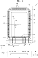
- FIG. 1 is a schematic plan view of a display device 1 according to an exemplary embodiment of the present disclosure.
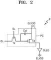
- FIG. 2 is an equivalent circuit diagram of a pixel P of a display device 1 according to an exemplary embodiment of the present disclosure.
- the display device 1 includes a display unit 10 disposed on a substrate 100.
- the display unit 10 includes multiple pixels P that are each connected to a scan line SL extending in a y direction and a data line DL extending in an x direction intersecting with the y direction.
- the display unit 10 displays an image via light emitted from the pixels P.
- a region of the display unit 10 in which the pixels P are disposed is defined as a display area DA, and thus an image is capable of being displayed within the display area DA.
- Each of the pixels P may emit, for example, one of a red light, green light, blue light, or white light.
- Each of the pixels P includes a display element, and the display element may include an organic light-emitting diode.
- the display area DA may include a first set of pixels that emit red light, a second set of pixels that emit green light, a third set of pixels that emit blue light, and optionally, a fourth set of pixels that emit white light.
- These various types of pixels may be interspersed in a desired pattern so as to be able to display any desired color near any particular region of the display area DA. In this manner, a desired image may be displayed within the display area DA.
- each pixel P may include a pixel circuit PC, connected to the scan line SL and the data line DL of that pixel P, and an organic light-emitting diode OLED connected to the pixel circuit PC.
- the pixel circuit PC includes a driving thin film transistor (TFT) Td, a switching TFT Ts, and a storage capacitor Cst.
- the switching TFT Ts is connected to the scan line SL and the data line DL, and is configured to transmit, to the driving TFT Td, a data signal received via the data line DL according to a scan signal received via the scan line SL.
- the storage capacitor Cst is connected to the switching TFT Ts and a driving voltage line PL, and is configured to store a voltage corresponding to a difference between a voltage received from the switching TFT Ts and a driving voltage ELVDD supplied to the driving voltage line PL.
- the driving TFT Td is connected to the driving voltage line PL and the storage capacitor Cst, and may be used to control a driving current flowing from the driving voltage line PL to the organic light-emitting diode OLED, in accordance with a voltage value stored in the storage capacitor Cst.
- the organic light-emitting diode OLED may emit light having a desired brightness by the driving current.
- the organic light-emitting diode OLED may emit, for example, red light, green light, blue light, or white light.
- the pixel circuit PC of the pixel P may include three or more TFTs or two or more storage capacitors. In this way, various modifications may be made to the described arrangement while keeping within the spirit and scope of the present disclosure.
- a peripheral area PA is arranged outside the display area DA.
- the peripheral area PA may surround the display area DA.
- the peripheral area PA is an area where no pixels P are arranged, and the peripheral area PA corresponds to a non-display area where no images are provided.
- a driving circuit for example, first and second scan driving circuits 20 and 30, a terminal unit 40, a driving power supply line 60, and a common power supply line 70 may be arranged.
- the first and second scan driving circuits 20 and 30 are arranged on the peripheral area PA of the substrate 100, and these first and second scan driving circuits 20 and 30 may be configured to generate and transmit a scan signal to each of the pixels P via the scan line SL.
- the first scan driving circuit 20 may be disposed on the left side of the display unit 10 and the second scan driving circuit 30 may be disposed on the right side of the display unit 10.
- other arrangements of the pixel and first and second scan driving circuits 20 and 30 may be provided.
- the terminal unit 40 is disposed on one side of the substrate 100 and includes a plurality of terminals 41, 42, 44, and 45.
- the terminal unit 40 may be exposed, i.e., might not be covered with an insulating layer, and thus may be electrically connected to a flexible printed circuit board FPCB.
- the terminal unit 40 may be disposed on one side of the substrate 100 where the first and second scan driving circuits 20 and 30 are not located.
- the flexible printed circuit board FPCB electrically connects a controller 90 to the terminal unit 40, and a signal or power received from the controller 90 travels along connection lines 21, 31, 51, 61, and 71 from the terminal unit 40.
- the controller 90 may receive a vertical synchronization signal, a horizontal synchronization signal, and a clock signal and may generate a control signal for controlling the driving of the first and second scan driving circuits 20 and 30.
- the generated control signal may be transmitted to each of the first and second scan driving circuits 20 and 30 via the terminal 44 connected with the flexible printed circuit board FPCB and the connection lines 21 and 31.
- the scan signal of the first and second scan driving circuits 20 and 30 may be provided to each of the pixels P via the scan line SL.
- the controller 90 provides driving voltage (driving power) ELVDD and common voltage (common power) ELVSS to the driving power supply line 60 and the common power supply line 70, respectively, via the terminals 42 and 45 connected to the flexible printed circuit board FPCB and the connection lines 61 and 71.
- the driving power ELVDD may be provided to each of the pixels P via the driving voltage line PL
- the common power ELVSS may be provided to a common electrode of each of the pixels P.
- a data driving circuit 50 may be disposed on the flexible printed circuit board FPCB.
- the data driving circuit 50 provides a data signal to each of the pixels P.
- the data signal of the data driving circuit 50 is provided to each of the pixels P via the connection line 51 connected to the terminal 41 and the data line DL connected to the connection line 51.
- the data driving circuit 50 is disposed on the flexible printed circuit board FPCB in FIG. 1
- exemplary embodiments of the present disclosure may utilize another configuration of the data driving circuit 50.
- the data driving circuit 50 may be disposed on the peripheral area PA of the substrate 100.
- the driving power supply line 60 may be disposed on the peripheral area PA.
- the driving power supply line 60 may be disposed between one side of the display unit 10, that is adjacent to the terminal unit 40, and the terminal unit 40.
- the driving power ELVDD is provided via the connection line 61 and terminal 42 to the driving power supply line 60, and may be provided to each of the pixels P via the driving voltage line PL.
- the common power supply line 70 may be disposed on the peripheral area PA, and may at least partially surround the display unit 10.
- the common power supply line 70 has an open loop shape in which the side of the display unit 10 adjacent to the terminal unit 40 is open.
- the common power supply line 70 may extend along edges of the substrate 100 except for the edge that includes the terminal unit 40.
- the common power supply line 70 is electrically connected to the terminal 45 via the connection line 71, and the common power supply line 70 provides the common power ELVSS to a common electrode (for example, a cathode) of the organic light-emitting diode OLED of the pixel P.
- the connection line 71 is shown as having an open loop shape in which one side partially surrounding the display unit 10 is open, and the connection line 71 overlaps the common power supply line 70.
- the connection line 71 partially surrounds the display unit 10, similar to the common power supply line 70.
- the connection line 71 may extend further toward one edge of the substrate 100 (e.g. the terminal unit 40) than the common power supply line 70 does.
- an encapsulation substrate 300 is disposed to face the substrate 100.
- a sealing material 400 is disposed between the substrate 100 and the encapsulation substrate 300.
- the sealing material 400 may at least partially surround the display unit 10.
- the sealing material 400 may entirely surround the display unit 10, as viewed from a plan view as shown in FIG. 1 .
- a space defined by the substrate 100, the encapsulation substrate 300, and the sealing material 400 may be spatially separated from the outside and thus may prevent infiltration of external moisture or impurities.
- the sealing material 400 is shown as entirely surrounding the display unit 10 and the first and second scan driving circuits 20 and 30. This may be understood as the display unit 10 and the first and second scan driving circuits 20 and 30 being arranged in a space (internal space) defined by the substrate 100, the encapsulation substrate 300, and the sealing material 400.
- the sealing material 400 may include, for example, an inorganic material, such as frit, but exemplary embodiments of the present disclosure may utilize other types of sealing materials.
- the sealing material 400 may include an epoxy or the like.
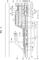
- FIG. 3 is a cross-sectional view of a portion of a display device according to an exemplary embodiment of the present disclosure, and the cross-section shown may correspond to a cross-section taken along line III-III' of FIG. 1 .
- the display device includes the display area DA and the peripheral area PA. Both the substrate 100 and the encapsulation substrate 300 may include areas corresponding to the display area DA and the peripheral area PA.
- the substrate 100 may be formed of any of various materials, for example, glass, metal, or plastic such as polyethylene terephthalate (PET), polyethylene naphthalate (PEN), or polyimide (PI).
- PET polyethylene terephthalate
- PEN polyethylene naphthalate
- PI polyimide
- the encapsulation substrate 300 may be substantially transparent and may include a transparent material.
- the encapsulation substrate 300 may be formed of any of various materials, for example, glass, or plastic such as PET, PEN, or PI.
- the substrate 100 and the encapsulation substrate 300 may include the same material or different materials.
- a buffer layer 101 may be formed on the substrate 100.
- the buffer layer 101 may block foreign matter or moisture from entering via the substrate 100.
- the buffer layer 101 may include an inorganic material, such as silicon oxide (SiOx), silicon nitride (SiNx), and/or silicon oxynitride (SiON), and may be formed as a multi-layer or a single layer.
- a TFT 130, a storage capacitor 140 and an organic light-emitting diode, as a display element 200, is located at a location corresponding to the display area DA.
- the organic light-emitting diode is electrically connected to the TFT 130 and the storage capacitor 140.
- the TFT 130 of FIG. 3 may correspond to one of the TFTs included in the pixel circuit PC described above with reference to FIG. 2 , for example, the driving TFT Td.
- the storage capacitor 140 of FIG. 3 may correspond to the storage capacitor Cst described above with reference to FIG. 2 .
- the TFT 130 includes a semiconductor layer 134 and a gate electrode 136.
- the semiconductor layer 134 may include, for example, polysilicon.
- the semiconductor layer 134 may include a channel region 131 that is overlapped by the gate electrode 136, and a source region 132 and a drain region 133 disposed on both sides of the channel region 131, respectively.
- the source region 132 and the drain region 133 may each include a higher concentration of impurities than the channel region 131.
- the impurities may include N-type impurities or P-type impurities.
- the source region 132 and the drain region 133 may be understood as a source electrode and a drain electrode of the TFT 130.
- the semiconductor layer 134 contains polysilicon.
- exemplary embodiments of the present disclosure are not limited to this particular composition of the semiconductor layer 134.
- the semiconductor layer 134 may include amorphous silicon or an organic semiconductor material.
- the semiconductor layer 134 may include an oxide semiconductor.
- the pixel circuit PC may include the driving TFT Td and the switching TFT Ts described above with reference to FIG. 2 , and a semiconductor layer of the driving TFT Td and a semiconductor layer of the switching TFT Ts may include different materials.
- one of the semiconductor layer of the driving TFT Td and the semiconductor layer of the switching TFT Ts may include an oxide semiconductor, and the other may include polysilicon.
- a gate insulating layer 103 may be disposed between the semiconductor layer 134 and the gate electrode 136.
- the gate insulating layer 103 may be an inorganic insulating layer including silicon oxynitride (SiON), silicon oxide (SiOx), and/or silicon nitride (SiNx).
- the inorganic insulating layer may be formed as a multi-layer or as a single layer.
- the storage capacitor 140 includes a first storage capacitor plate 144 and a second storage capacitor plate 146 that overlap each other.
- a first interlayer insulating layer 105 may be disposed between the first and second storage capacitor plates 144 and 146.
- the first interlayer insulating layer 105 has a certain permittivity, and may be an inorganic insulating layer including silicon oxynitride (SiON), silicon oxide (SiOx), and/or silicon nitride (SiNx), and may be formed as a multi-layer or a single layer.
- the storage capacitor 140 overlaps the TFT 130, and the first storage capacitor plate 144 is the gate electrode 136 of the TFT 130.
- exemplary embodiments of the present disclosure may have other arrangements.
- the storage capacitor 140 might not overlap the TFT 130, and the first storage capacitor plate 144 may be a component independent from the gate electrode 136 of the TFT 130.
- the storage capacitor 140 may be covered with a second interlayer insulating layer 107.
- the second interlayer insulating layer 107 may be an inorganic insulating layer including silicon oxynitride (SiON), silicon oxide (SiOx), and/or silicon nitride (SiNx).
- the second interlayer insulating layer 107 may be formed as a multi-layer or a single layer.
- a driving voltage line PL may be disposed on a first organic insulating layer 111.
- the driving voltage line PL may include aluminum (Al), copper (Cu), and/or titanium (Ti), and may be formed as a single layer or as a multi-layer.
- the driving voltage line PL may have a multi-layer structure of Ti/Al/Ti.
- FIG. 3 shows a lower driving voltage line PL1 disposed below the first organic insulating layer 111.
- the lower driving voltage line PL1 may be electrically connected to the driving voltage line PL via a contact hole that penetrates through the first organic insulating layer 111, and may prevent a voltage drop of the driving voltage ELVDD provided via the driving voltage line PL.
- the lower driving voltage line PL1 may include a material that is the same as that included in the data line DL.
- the lower driving voltage line PL1 and the data line DL may include Al, Cu, and/or Ti, and may be formed as a single layer or as a multi-layer.
- the lower driving voltage line PL1 and the data line DL may have a multi-layer structure, such as Ti/Al/Ti or TiN/Al/Ti.
- the first organic insulating layer 111 includes an organic insulating material.
- the organic insulating material may include an imide-based polymer, a general polymer such as polymethyl methacrylate (PMMA) or polystyrene (PS), a polymer derivative having a phenol-based group, an acryl-based polymer, an aryl ether-based polymer, an amide-based polymer, a fluorine-based polymer, a p-xylene-based polymer, a vinyl alcohol-based polymer, a blend thereof, and/or the like.
- the first organic insulating layer 111 may include polymide.
- the driving voltage line PL may be covered with a second organic insulating layer 113.
- the second organic insulating layer 113 may include a general polymer such as PMMA or PS, a polymer derivative having a phenol-based group, an acryl-based polymer, an imide-based polymer, an acryl ether-based polymer, an amide-based polymer, a fluorine-based polymer, a p-xylene-based polymer, a vinyl alcohol-based polymer, a blend thereof, or the like.
- the second organic insulating layer 113 may include polymide.
- a pixel electrode 210 is disposed on the second organic insulating layer 113.
- a pixel defining layer 120 may be disposed on the pixel electrode 210.
- the pixel defining layer 120 may define pixels by including respective openings corresponding to sub-pixels, namely, an opening via which at least a center portion of the pixel electrode 210 is exposed.
- the pixel defining layer 120 may prevent electrical arcing, or the like, from occurring between an edge of the pixel electrode 210 and a common electrode 230 of the display element 200, by increasing a distance between the edge of the pixel electrode 210 and the common electrode 230.
- the pixel defining layer 120 may be formed of an organic material, for example, polyimide or hexamethyldisiloxane (HMDSO).
- An intermediate layer 220 may include a low-molecular weight or high-molecular weight material.
- the intermediate layer 220 may have a structure in which a hole injection layer (HIL), a hole transport layer (HTL), an emission layer (EML), an electron transport layer (ETL), and an electron injection layer (EIL) are stacked in a single or complex structure, and may include various organic materials including copper phthalocyanine (CuPc), N,N'-Di(naphthalene-1-yl)-N,N'-diphenyl-benzidine (NPB), and tris-8-hydroxyquinoline aluminum (Alq3). These layers may be formed via vacuum deposition.
- HIL hole injection layer
- HTL hole transport layer
- EML emission layer
- ETL electron transport layer
- EIL electron injection layer
- Alq3 tris-8-hydroxyquinoline aluminum
- the intermediate layer 220 may additionally include an HTL and an EML.
- the HTL may include poly(ethylenedioxythiophene) (PEDOT)
- the EML may include a high-molecular weight material such as a polyphenylenevinylene (PPV)-based material or a polyfluorene-based material.
- the intermediate layer 220 is not limited to the above-described structure, and may have any of various other structures. For example, at least one of the layers that constitute the intermediate layer 220 may extend over a plurality of pixel electrodes 210. Alternatively, the intermediate layer 220 may include a layer patterned to correspond to each of the plurality of pixel electrodes 210.
- the common electrode 230 may be disposed on the display area DA and may cover the display area DA.
- the common electrode 230 may be formed as a single body such as to cover a plurality of pixels.
- a filling material 500 may be disposed between the common electrode 230 and the encapsulation substrate 300.
- the filling material 500 may include a photo-curable epoxy-based material and/or an acrylate-based material, but other arrangements may alternatively be used.
- a driving circuit for example, the first scan driving circuit 20, is disposed on the substrate 100.
- the first scan driving circuit 20 may include thin film transistors TFT-P, and may include a line connected with the thin film transistors TFT-P.
- the thin film transistors TFT-P may be formed together with the TFTs of the pixel circuit PC as part of the same process step.
- the first scan driving circuit 20 includes an insulating layer interposed between components (for example, interposed between a semiconductor layer and a gate electrode) of the thin film transistor TFT-P.
- the buffer layer 101, the gate insulating layer 103, and the first and second interlayer insulating layers 105 and 107 may extend to the peripheral area PA to thereby form an insulating layer 110.
- the insulating layer 110 includes an inorganic insulating material.
- An inorganic insulating layer 109 may be disposed on the first scan driving circuit 20.
- the first scan driving circuit 20 may be covered with the inorganic insulating layer 109.
- the inorganic insulating layer 109 may prevent exposure, to an etching environment, of a connection line 71 including metal that may be damaged by an etchant, like aluminum, during the manufacture of the display device.
- the inorganic insulating layer 109 is also disposed on the display area DA.
- the inorganic insulating layer 109 may include an inorganic material, such as silicon oxide (SiOx), silicon nitride (SiNx), and/or silicon oxynitride (SiON), and may be formed as a multi-layer or a single layer. According to an exemplary embodiment of the present disclosure, the inorganic insulating layer 109 may include SiNx. The inorganic insulating layer 109 may have a thickness of at least about 500 ⁇ .
- a thickness of the inorganic insulating layer 109 may be equal to or greater than 1,000 ⁇ , may be equal to or greater than 1,500 ⁇ , may be equal to or greater than 2,000 ⁇ , may be equal to or greater than 2,500 ⁇ , may be equal to or greater than 3,000 ⁇ , may be equal to or greater than 3,500 ⁇ , may be equal to or greater than 4,000 ⁇ , may be equal to or greater than 4,500 ⁇ , may be equal to or greater than 5,000 ⁇ , may be equal to or greater than 5,500 ⁇ , may be equal to or greater than 6,000 ⁇ , or may be equal to or greater than 6,500 ⁇ .
- the inorganic insulating layer 109 may have a thickness of about 7,000 ⁇ to about 10,000 ⁇ .
- the common power supply line 70 overlaps the first scan driving circuit 20 with the inorganic insulating layer 109 interposed therebetween.
- the common power supply line 70 may include a material that is the same as that included in the driving voltage line PL.
- the first scan driving circuit 20 is entirely covered with the common power supply line 70 and thus may be prevented from being damaged by static electricity.
- the common power supply line 70 includes through holes such that gases remaining in the organic insulating layer may be discharged therethrough.
- a first width W1 of the common power supply line 70 may be greater than a width of the first scan driving circuit 20 or a width of a driving circuit area DPC-A on which the first scan driving circuit 20 is disposed.
- the common power supply line 70 may have a first end 70E1, that is closes to the TFT 130, and a second end 70E2, that is farthest from the TFT 130, as seen in the cross-sectional view.
- the first end 70E1 of the common power supply line 70 may extend beyond the driving circuit area DPC-A toward a display unit (display region DA).
- the second end 70E2 of the common power supply line 70 which is opposite to the first end 70E1 in a width direction, may extend beyond the driving circuit area DPC-A toward an edge 100E of the substrate 100.
- the first organic insulating layer 111 is interposed between the first end 70E1 of the common power supply line 70 and the inorganic insulating layer 109, in a z direction. If the first organic insulating layer 111 extends to cover the driving circuit area DPC-A, a through hole configured to discharge gas remaining in the first organic insulating layer 111 needs to be formed in the common power supply line 70, and this may lead to the first organic insulating layer 111 being damaged during the formation of the sealing material 400, or another related problem. Thus, the first organic insulating layer 111 is patterned to expose (i.e. not cover) the driving circuit area DPC-A. Accordingly, an end 111E of the first organic insulating layer 111 may be located between the first scan driving circuit 20 and the display area DA and/or between the driving circuit area DPC-A and the display area DA.
- the first end 70E1 of the common power supply line 70 may be covered with the second organic insulating layer 113. Therefore, a problem may occur when the first end 70E1 of the common power supply line 70 is exposed without being covered with the second organic insulating layer 113. For example, during etching of the pixel electrode 210, the first end 70E1 of the common power supply line 70 may be damaged, or unwanted particles may be formed due to extraction of a material included in the common power supply line 70.
- the second organic insulating layer 113 is also patterned to expose (i.e. not cover) the driving circuit area DPC-A and/or the first scan driving circuit 20.
- An end 113E of the second organic insulating layer 113 may be located between the first scan driving circuit 20 and the display area DA and/or between the driving circuit area DPC-A and the display area DA.
- the end 111E of the first organic insulating layer 111 extends further toward the edge 100E of the substrate 100 than the end 113E of the second organic insulating layer 113 does.
- the end 113E of the second organic insulating layer 113 may be covered with a conductive layer 75 including a material that is the same as that included in the pixel electrode 210.
- the conductive layer 75 covers a lateral surface of the end 113E of the second organic insulating layer 113 and contacts an upper surface of the common power supply line 70 disposed below the end 113E of the second organic insulating layer 113.
- the conductive layer 75 may include a through hole configured to discharge gas remaining in the second organic insulating layer 113.
- a portion of the conductive layer 75 that contacts the second organic insulating layer 113 may include a through hole configured to discharge gas remaining in the second organic insulating layer 113.
- the common power supply line 70 at least partially covers the connection line 71 located between the edge 100E of the substrate 100 and the first scan driving circuit 20 and/or the driving circuit area DPC-A. In some implementations, the common power supply line 70 entirely covers the connection line 71 as shown in Fig. 3 . In some implementations, the second end 70E2 of common power supply line 70 may extends to the edge 100E of the substrate 100 beyond the connection line 71.
- the connection line 71 and the common power supply line 70 may be electrically connected to each other and may contact each other through a contact hole 109H of the inorganic insulating layer 109.
- the sealing material 400 is disposed on the common power supply line 70, and may overlap the second end 70E2 of the common power supply line 70 and the first scan driving circuit 20.
- the sealing material 400 may include frit, epoxy, or the like, as described above.
- the frit may be a paste including a laser or infrared absorbing material, an organic binder, and/or a filler for reducing a thermal expansion coefficient, and the like, that is disposed within a main material, such as SiO 2 .
- the frit paste may be hardened by removing the organic binder and moisture via a drying or firing process.
- the laser or infrared absorbing material may include a transition metal compound. After drying or firing, laser light may be used as a heat source for hardening the sealing material 400.
- the laser light may reach the second end 70E2 of the common power supply line 70 that overlaps the sealing material 400.
- an upper surface of at least one of first through third metal layers 70A, 70B, and 70C that constitute the second end 70E2 of the common power supply line 70 may become an irregular surface, as shown in a magnified view of FIG. 3 .
- the magnified view of FIG. 3 shows that the first through third metal layers 70A, 70B, and 70C of the common power supply line 70 have a three-layered structure of Ti/Al/ Ti or TiN/Al/Ti.
- the common power supply line 70 is electrically connected to the common electrode 230 of the display element 200.
- An end 230E of the common electrode 230 may extend over/onto the first scan driving circuit 20 beyond a dummy pixel region DPX of the peripheral area PA and may directly contact the common power supply line 70.
- the end 230E of the common electrode 230 may be disposed a certain distance away from an inner sidewall 400IS of the sealing material 400.
- the common power supply line 70 has the first width W1 and entirely covers the first scan driving circuit 20, damage to the first scan driving circuit 20 by static electricity may be prevented, a voltage drop of the common voltage ELVSS (see FIG. 2 ) applied to the common electrode 230 may be prevented due to prevention of a resistance increase of the common power supply line 70, and power consumption of the display device may be reduced.
- the common power supply line 70 has the first width W1 and entirely covers the first scan driving circuit 20
- the width of a portion of the connection line 71 between the edge 100E of the substrate 100 and the first scan driving circuit 20 may be reduced without the voltage drop of the common voltage ELVSS (see FIG. 2 ) applied to the common electrode 230, and accordingly, the width of the peripheral area PA of the display device may be reduced.
- FIG. 4 is a cross-sectional view of a display device according to an exemplary embodiment of the present disclosure, and may correspond to a cross-section taken along line III-III' of FIG. 1 . All components of the display device of FIG. 4 except for the ends 111E and 113E of the first and second organic insulating layers 111 and 113, the conductive layer 75, and components related therewith may be considered to be at least similar to those corresponding elements described above with reference to FIG. 3 , and thus differences between FIGS. 3 and 4 will now be focused on and described.
- Each of the ends 111E and 113E of the first and second organic insulating layers 111 and 113 is disposed between the first scan driving circuit 20 and the display area DA and/or between the driving circuit area DPC-A and the display area DA.
- the end 113E of the second organic insulating layer 113 may extend further toward the first scan driving circuit 20 and/or the driving circuit area DPC-A than the end 111E of the first organic insulating layer 111 does, but the end 113E of the second organic insulating layer 113 does not cover the first scan driving circuit 20.
- the end 113E of the second organic insulating layer 113 may be covered with the conductive layer 75.
- the conductive layer 75 may cover the lateral surface of the end 113E of the second organic insulating layer 113 and at the same time may contact the upper surface of the common power supply line 70 disposed below the end 113E of the second organic insulating layer 113.
- a portion of the conductive layer 75 that contacts the second organic insulating layer 113 may include a through hole configured to discharge gas remaining in the second organic insulating layer 113.
- FIG. 5 is a cross-sectional view of a display device according to an exemplary embodiment of the present disclosure, and may correspond to a cross-section taken along line III-III' of FIG. 1 . All components of the display device of FIG. 5 except for the common electrode 230, the conductive layer 75, and components related therewith may be at least similar to those corresponding elements described above with reference to FIG. 3 , and thus differences between FIGS. 3 and 5 will now be focused on and described.
- the end 230E of the common electrode 230 may be overlapped by the sealing material 400.
- the end 230E of the common electrode 230 may be disposed between the inner sidewall 400IS of the sealing material 400 and an outer sidewall 400OS thereof.
- the first scan driving circuit 20 may be effectively protected from static electricity, due to a multi-layered structure of the common power supply line 70 and the common electrode 230.
- a contact surface between the common electrode 230 and the common power supply line 70 increases, a voltage drop of the common voltage ELVSS (see FIG. 2 ) applied to the common electrode 230 may be prevented, and power consumption of the display device may be reduced.
- the common electrode 230 entirely covers the first scan driving circuit 20 and/or the driving circuit area DPC-A.
- the common electrode 230 may be at least partially overlapped by the sealing material 400, but the common electrode 230 may cover only a portion of the first scan driving circuit 20 and/or the driving circuit area DPC-A.
- the conductive layer 75 may cover a lateral surface of the end 113E of the second organic insulating layer 113 but may extend to the first scan driving circuit 20 and/or the driving circuit area DPC-A.
- the conductive layer 75 may at least partially cover a portion of the first scan driving circuit 20.
- the conductive layer 75 may directly contact the common power supply line 70. Because no insulating layers (e.g., no organic insulating layers) might be interposed between the conductive layer 75 and the common power supply line 70, a problem related to outgasing that may otherwise occur by an organic insulating layer is prevented. Accordingly, no through holes need be formed in a portion of the conductive layer 75 that overlaps the common power supply line 70.
- an end 75E of the conductive layer 75 is disposed on the first scan driving circuit 20 and contacts the common power supply line 70, but is a certain distance away from the inner sidewall 400IS of the sealing material 400 and is located further toward the inside of the display device than the end 230E of the common electrode 230.
- the end 75E of the conductive layer 75 may extend past the first scan driving circuit 20 and may be interposed between the inner sidewall 400IS and the outer sidewall 400OS of the sealing material 400, and may be overlapped by the sealing material 400.
- the ends 111E and 113E of the first and second organic insulating layers 111 and 113 and the conductive layer 75 from among the components of the display device of FIG. 5 may have the same structures as those shown in FIG. 4 .
- FIG. 6 is a plan view illustrating a display device 2 according to an exemplary embodiment of the present disclosure.
- the display device 2 of FIG. 6 is different from the display device 1 described above with reference to FIGS. 1 and 2 in terms of a connection line 71' and components related therewith. To the extent that the description of elements are not provided herein, it may be assumed that these elements are at least similar to corresponding elements that have already been described with respect to FIGS. 1 and 2 .
- connection line 71' connects the common power supply line 70 of the display device 2 with the terminal 45 of the terminal unit 40, and may be located between one side of the display unit 10 and the terminal unit 40.
- the connection line 71' may be interposed between the terminal unit 40 and one side of the display unit 10 adjacent to the terminal unit 40.
- the connection line 71' may be electrically connected to the common power supply line 70 having an open loop shape in which one side partially surrounding the display unit 10 is open.
- the connection line 71' and the common power supply line 70 may be connected to each other via a contact hole CNT of an insulating layer, for example, an inorganic insulating layer, interposed therebetween.
- a contact area between the connection line 71' and the common power supply line 70, namely, the contact hole CNT may be an area adjacent to one side of the display unit 10 that faces the terminal unit 40.
- connection line 71 of the display device 1 of FIG. 1 has an open loop shape, and may be connected to the common power supply line 70 while overlapping the common power supply line 70, a connection area between the connection line 71 and the common power supply line 70 has an open loop shape similar to that of the common power supply line 70.
- the connection line 71 overlaps with the common power supply line 70.
- a connection area between the connection line 71' and the common power supply line 70 of FIG. 6 may be limited to an area adjacent to one side of the display unit 10 that faces the terminal unit 40.
- connection line 71' is not located around a driving circuit (for example, the first and second scan driving circuits 20 and 30) on the peripheral area PA of the display device 2, the peripheral area PA, for example, the peripheral area PA around the driving circuit, may have a reduced width.
- FIG. 7 is a cross-sectional view of a display device according to an exemplary embodiment of the present invention, and FIG. 7 corresponds to a cross-section taken along line VII- VII' of FIG. 6 .
- connection lines 71' are located on a peripheral area PA where a driving circuit, for example, the first scan driving circuit 20, is located. Because no connection lines 71' are arranged on the peripheral area PA around the first scan driving circuit 20 as described above with reference to FIG. 6 , the peripheral area PA may have a more reduced width. Because the display area DA of FIG. 7 is the same as the display area DA described above with reference to FIG. 3 , the peripheral area PA will now be focused on and described.
- the driving circuit for example, the first scan driving circuit 20, may be disposed on the substrate 100, and the first scan driving circuit 20 may include thin film transistors TFT-P and a line connected with the thin film transistors TFT-P.
- the thin film transistors TFT-P may be formed together with the TFTs of the pixel circuit PC as part of the same process step.
- the first scan driving circuit 20 includes an insulating layer(s) interposed between components (for example, a semiconductor layer and a gate electrode) of the thin film transistor TFT-P.
- At least one of the buffer layer 101, the gate insulating layer 103, and the first and second interlayer insulating layers 105 and 107 may extend to the peripheral area PA to thereby form an insulating layer 110.
- the insulating layer 110 is an inorganic insulating layer.
- the first scan driving circuit 20 is covered with the inorganic insulating layer 109, and a thickness, a material, and the like of the inorganic insulating layer 109 are the same as those described above with reference to FIG. 3 .
- the inorganic insulating layer 109 is also disposed on the display area DA.
- the common power supply line 70 overlaps the first scan driving circuit 20. Only an insulating layer of an inorganic insulating material, such as the inorganic insulating layer 109, is interposed between the first scan driving circuit 20 and the common power supply line 70.
- the common power supply line 70 may include a material that is the same as that included in the driving voltage line PL.
- the first scan driving circuit 20, covered with the common power supply line 70 may be protected from static electricity. Because no organic insulating layers are interposed between the common power supply line 70 and the first scan driving circuit 20, discharge of remaining gas that occur when an organic insulating layer is interposed therebetween is prevented. Thus, as described above, no through holes are formed in the common power supply line 70, in more detail, in a portion of the common power supply line 70 that overlaps the first scan driving circuit 20 and the inorganic insulating layer 109.
- a first width W1' of the common power supply line 70 may be greater than a width of the first scan driving circuit 20 or a width of a driving circuit area DPC-A on which the first scan driving circuit 20 is disposed.
- a first end 70E1 of the common power supply line 70 may extend beyond the driving circuit area DPC-A toward a display unit (display region DA), and a second end 70E2 of the common power supply line 70, which is an opposite to the first end 70E1, may extend beyond the driving circuit area DPC-A toward an edge 110E of the substrate 100.
- the first end 70E1 of the common power supply line 70 is disposed on the first organic insulating layer 111 and is covered with the second organic insulating layer 113.
- the ends 111E and 113E of the first and second organic insulating layers 111 and 113 are certain distances away from the sealing material 400, respectively.
- the ends 111E and 113E of the first and second organic insulating layers 111 and 113 may be located in an inner side of the first scan driving circuit 20, namely, the driving circuit area DPC-A, such that they do not cover the first scan driving circuit 20.
- the end 113E of the second organic insulating layer 113 may be covered with a conductive layer 75 including a material that is the same as that included in the pixel electrode 210.
- the second end 70E2 of the common power supply line 70 extends further toward the edge 100E of the substrate 100 beyond the first scan driving circuit 20 and/or the driving circuit area DPC-A.
- the second end 70E2 of the common power supply line 70 may be overlapped by the sealing material 400 and may be located between the inner sidewall 400IS and the outer sidewall 400OS of the sealing material 400.
- an area EPA between the first scan driving circuit 20 and the edge 100E of the substrate 100 or between the driving circuit area DPC-A and the edge 100E of the substrate 100 may have a smaller width than that described above with reference to FIG. 3 .
- the sealing material 400 is disposed on the common power supply line 70, and may at least partially overlap the common power supply line 70 and the first scan driving circuit 20.
- the sealing material 400 may include frit, epoxy, or the like, as described above.
- the common power supply line 70 is electrically connected to the common electrode 230 of the display element 200.
- An end 230E of the common electrode 230 may extend over/onto the first scan driving circuit 20 beyond a dummy pixel region DPX of the peripheral area PA and may directly contact the common power supply line 70.
- the end 230E of the common electrode 230 may be a certain distance away from the inner sidewall 400IS of the sealing material 400.
- FIG. 8 is a cross-sectional view of a display device according to an exemplary embodiment of the present disclosure, and may correspond to a cross-section taken along line VII-VII' of FIG. 6 . All components of the display device of FIG. 8 except for the ends 111E and 113E of the first and second organic insulating layers 111 and 113, the conductive layer 75, and components related therewith are at least similar to those described above with reference to FIG. 7 , and thus differences between FIGS. 7 and 8 will now be focused on and described.
- Each of the ends 111E and 113E of the first and second organic insulating layers 111 and 113 is disposed between the first scan driving circuit 20 and the display area DA and/or between the driving circuit area DPC-A and the display area DA.
- the end 113E of the second organic insulating layer 113 may extend further toward the first scan driving circuit 20 and/or the driving circuit area DPC-A than the end 111E of the first organic insulating layer 111 does, but the end 113E of the second organic insulating layer 113 does not cover the first scan driving circuit 20.
- the end 113E of the second organic insulating layer 113 may be covered with the conductive layer 75.
- the conductive layer 75 may cover the lateral surface of the end 113E of the second organic insulating layer 113 and at the same time may contact the upper surface of the common power supply line 70 disposed below the end 113E of the second organic insulating layer 113.
- a portion of the conductive layer 75 that contacts the second organic insulating layer 113 may include a through hole configured to discharge gas remaining in the second organic insulating layer 113.
- FIG. 9 is a cross-sectional view of a display device according to an exemplary embodiment of the present disclosure, and may correspond to a cross-section taken along line VII-VII' of FIG. 6 . All components of the display device of FIG. 9 except for the common electrode 230, the conductive layer 75, and components related therewith are at least similar to corresponding elements described above with reference to FIG. 7 , and thus differences between FIGS. 7 and 9 will now be focused on and described.
- the end 230E of the common electrode 230 may be overlapped by the sealing material 400.
- the end 230E of the common electrode 230 may be disposed between the inner sidewall 400IS of the sealing material 400 and the outer sidewall 400OS thereof.
- the first scan driving circuit 20 may be effectively protected from static electricity, due to a multi-layered structure of the common power supply line 70 and the common electrode 230.
- a contact surface between the common electrode 230 and the common power supply line 70 increases, a voltage drop of the common voltage ELVSS (see FIG. 2 ) applied to the common electrode 230 may be prevented, and power consumption of the display device may be reduced.
- the common electrode 230 entirely covers the first scan driving circuit 20 and/or the driving circuit area DPC-A in FIG. 9 , other configurations may be used. According to an exemplary embodiment of the present disclosure, the common electrode 230 may be overlapped by the sealing material 400, and may cover only a portion of the first scan driving circuit 20 and/or the driving circuit area DPC-A.
- the conductive layer 75 may cover a lateral surface of the end 113E of the second organic insulating layer 113 and may extend to the first scan driving circuit 20 and/or the driving circuit area DPC-A.
- the conductive layer 75 may cover at least a portion of the first scan driving circuit 20.
- the conductive layer 75 may directly contact the common power supply line 70. Because no insulating layers (e.g., no organic insulating layers) are interposed between the conductive layer 75 and the common power supply line 70, a problem related to outgasing that may occur by an organic insulating layer is prevented. Thus, a portion of the conductive layer 75 that overlaps the common power supply line 70 does not need to include a through hole or the like.
- the end 75E of the conductive layer 75 is disposed on the first scan driving circuit 20 and contacts the common power supply line 70, and is located between the inner sidewall 400IS and the outer sidewall 400OS of the sealing material 400. According to an exemplary embodiment of the present disclosure, the end 75E of the conductive layer 75 may be located further toward the inside of the display device than the inner sidewall 400IS of the sealing material 400, and thus might not be overlapped by the sealing material 400.
- the ends 111E and 113E of the first and second organic insulating layers 111 and 113 and the conductive layer 75 from among the components of the display device of FIG. 9 may have the same structures as those shown in FIG. 8 .
- cross-sections based on the first scan driving circuit 20 as a driving circuit have been described in FIGS. 3 through 5 and FIGS. 7 through 9
- cross-sections based on the second scan driving circuit 30 as a driving circuit may also have the same structures as the above-described structures.
- the driving circuit is a scan driving circuit.
- the driving circuit may be a data driving circuit or the like.
- the data driving circuit may be disposed on an upper side of the substrate 100 that is opposite to a lower side of the substrate 100 where the terminal unit 40 is disposed, on the plan views of FIGS. 1 and 6 .
- a structure of a cross-section of this case is substantially the same as that described above with reference to FIGS. 3 through 5 and FIGS. 7 through 9 except that the data driving circuit is disposed on the driving circuit area DPC-A.
Landscapes
- Engineering & Computer Science (AREA)
- Physics & Mathematics (AREA)
- Microelectronics & Electronic Packaging (AREA)
- Computer Hardware Design (AREA)
- General Physics & Mathematics (AREA)
- Theoretical Computer Science (AREA)
- Optics & Photonics (AREA)
- Geometry (AREA)
- Electroluminescent Light Sources (AREA)
- Devices For Indicating Variable Information By Combining Individual Elements (AREA)
Applications Claiming Priority (1)
| Application Number | Priority Date | Filing Date | Title |
|---|---|---|---|
| KR1020180007238A KR102546170B1 (ko) | 2018-01-19 | 2018-01-19 | 표시 장치 |
Publications (3)
| Publication Number | Publication Date |
|---|---|
| EP3525254A2 true EP3525254A2 (fr) | 2019-08-14 |
| EP3525254A3 EP3525254A3 (fr) | 2019-11-27 |
| EP3525254B1 EP3525254B1 (fr) | 2022-07-27 |
Family
ID=65041602
Family Applications (1)
| Application Number | Title | Priority Date | Filing Date |
|---|---|---|---|
| EP19152453.7A Active EP3525254B1 (fr) | 2018-01-19 | 2019-01-18 | Afficheur |
Country Status (4)
| Country | Link |
|---|---|
| US (3) | US11171195B2 (fr) |
| EP (1) | EP3525254B1 (fr) |
| KR (2) | KR102546170B1 (fr) |
| CN (1) | CN110061032B (fr) |
Families Citing this family (28)
| Publication number | Priority date | Publication date | Assignee | Title |
|---|---|---|---|---|
| KR102546170B1 (ko) | 2018-01-19 | 2023-06-22 | 삼성디스플레이 주식회사 | 표시 장치 |
| CN108717939B (zh) * | 2018-06-01 | 2020-06-12 | 京东方科技集团股份有限公司 | 静电释放保护电路、阵列基板和显示装置 |
| KR102664769B1 (ko) | 2018-08-20 | 2024-05-08 | 엘지디스플레이 주식회사 | 표시장치 |
| KR102799461B1 (ko) * | 2019-03-06 | 2025-04-23 | 삼성디스플레이 주식회사 | 표시 장치 |
| CN111857395B (zh) * | 2019-04-30 | 2025-01-17 | 群创光电股份有限公司 | 触控显示设备 |
| KR20210014265A (ko) * | 2019-07-29 | 2021-02-09 | 삼성디스플레이 주식회사 | 디스플레이 장치 |
| CN110600505A (zh) * | 2019-08-20 | 2019-12-20 | 武汉华星光电半导体显示技术有限公司 | Oled显示装置 |
| CN110444690B (zh) * | 2019-08-20 | 2022-03-04 | 京东方科技集团股份有限公司 | 显示基板及其制作方法、显示装置 |
| KR102895954B1 (ko) | 2019-10-17 | 2025-12-04 | 삼성디스플레이 주식회사 | 표시장치 |
| US12178094B2 (en) | 2019-11-06 | 2024-12-24 | Sharp Kabushiki Kaisha | Display device |
| CN110690365B (zh) * | 2019-11-08 | 2025-06-27 | 京东方科技集团股份有限公司 | 显示基板及其显示装置 |
| CN110993814B (zh) * | 2019-11-15 | 2021-09-03 | 深圳市华星光电半导体显示技术有限公司 | 显示装置及其制备方法 |
| KR102737535B1 (ko) * | 2019-11-28 | 2024-12-02 | 엘지디스플레이 주식회사 | 표시 장치 |
| CN111445860B (zh) * | 2020-04-30 | 2021-08-03 | 深圳市华星光电半导体显示技术有限公司 | 一种显示面板及其制作方法以及电子装置 |
| US11500248B2 (en) * | 2020-07-31 | 2022-11-15 | Innolux Corporation | Sealing structure and an electronic device having the same |
| KR102886501B1 (ko) * | 2020-08-21 | 2025-11-14 | 삼성디스플레이 주식회사 | 표시 장치 |
| JP7541880B2 (ja) * | 2020-09-14 | 2024-08-29 | キヤノン株式会社 | 有機発光装置、表示装置、光電変換装置、電子機器、照明装置、および移動体 |
| US12369464B2 (en) * | 2020-09-29 | 2025-07-22 | Samsung Display Co., Ltd. | Display device |
| KR102894204B1 (ko) * | 2020-10-22 | 2025-12-02 | 삼성디스플레이 주식회사 | 표시 장치 |
| GB2610955A (en) * | 2020-12-09 | 2023-03-22 | Boe Technology Group Co Ltd | Display substrate and display apparatus thereof |
| JP2022154586A (ja) * | 2021-03-30 | 2022-10-13 | 株式会社ジャパンディスプレイ | 表示装置 |
| KR20230006692A (ko) * | 2021-07-01 | 2023-01-11 | 삼성디스플레이 주식회사 | 표시 장치 |
| CN113690279B (zh) | 2021-08-04 | 2025-02-28 | 惠州华星光电显示有限公司 | 显示面板及电子设备 |
| KR102888744B1 (ko) * | 2021-08-26 | 2025-11-21 | 삼성디스플레이 주식회사 | 표시 장치 |
| JP2023106165A (ja) * | 2022-01-20 | 2023-08-01 | 株式会社ジャパンディスプレイ | 表示装置 |
| KR20230120151A (ko) * | 2022-02-07 | 2023-08-17 | 삼성디스플레이 주식회사 | 표시 장치 및 이의 제조 방법 |
| CN115295582B (zh) * | 2022-07-21 | 2025-10-17 | 武汉天马微电子有限公司 | 显示面板和显示装置 |
| CN119923089A (zh) * | 2025-01-21 | 2025-05-02 | 合肥维信诺科技有限公司 | 显示面板、显示面板的制备方法及显示装置 |
Family Cites Families (36)
| Publication number | Priority date | Publication date | Assignee | Title |
|---|---|---|---|---|
| US2017034A (en) | 1933-03-07 | 1935-10-15 | Avery William Leicester | Vehicle wheel |
| US6822264B2 (en) | 2001-11-16 | 2004-11-23 | Semiconductor Energy Laboratory Co., Ltd. | Light emitting device |
| US7038377B2 (en) * | 2002-01-16 | 2006-05-02 | Seiko Epson Corporation | Display device with a narrow frame |
| JP4593179B2 (ja) | 2003-06-17 | 2010-12-08 | 株式会社半導体エネルギー研究所 | 表示装置 |
| US7224118B2 (en) | 2003-06-17 | 2007-05-29 | Semiconductor Energy Laboratory Co., Ltd. | Display device and electronic apparatus having a wiring connected to a counter electrode via an opening portion in an insulating layer that surrounds a pixel electrode |
| KR20060082637A (ko) | 2005-01-13 | 2006-07-19 | 삼성전자주식회사 | 실란트 경화장치 및 이를 이용한 평판표시장치 |
| US7839083B2 (en) | 2007-02-08 | 2010-11-23 | Seiko Epson Corporation | Light emitting device and electronic apparatus |
| JP5401784B2 (ja) * | 2007-02-08 | 2014-01-29 | セイコーエプソン株式会社 | 発光装置 |
| JP2011003522A (ja) | 2008-10-16 | 2011-01-06 | Semiconductor Energy Lab Co Ltd | フレキシブル発光装置、電子機器及びフレキシブル発光装置の作製方法 |
| KR20110019498A (ko) * | 2009-08-20 | 2011-02-28 | 삼성모바일디스플레이주식회사 | 유기전계발광 표시장치 |
| KR101201720B1 (ko) * | 2010-07-29 | 2012-11-15 | 삼성디스플레이 주식회사 | 표시 장치 및 유기 발광 표시 장치 |
| US9673267B2 (en) | 2013-03-26 | 2017-06-06 | Lg Display Co., Ltd. | Organic light emitting diode display device having a capacitor with stacked storage electrodes and method for manufacturing the same |
| JP6182985B2 (ja) | 2013-06-05 | 2017-08-23 | セイコーエプソン株式会社 | 電気光学装置、電気光学装置の製造方法、電子機器 |
| KR20150043136A (ko) * | 2013-10-14 | 2015-04-22 | 삼성디스플레이 주식회사 | 유기 발광 표시 장치 및 이의 제조 방법 |
| KR102207563B1 (ko) | 2013-10-29 | 2021-01-27 | 삼성디스플레이 주식회사 | 유기 발광 표시장치 및 유기 발광 표시장치의 제조 방법 |
| KR102144084B1 (ko) | 2013-11-19 | 2020-08-14 | 삼성디스플레이 주식회사 | 터치 스크린 패널 일체형 표시장치 |
| KR102118676B1 (ko) * | 2014-02-05 | 2020-06-04 | 삼성디스플레이 주식회사 | 유기발광 디스플레이 장치 |
| KR102331171B1 (ko) * | 2014-08-01 | 2021-11-29 | 삼성디스플레이 주식회사 | 표시장치 및 그 제조방법 |
| KR102360783B1 (ko) * | 2014-09-16 | 2022-02-10 | 삼성디스플레이 주식회사 | 디스플레이 장치 |
| KR102284756B1 (ko) * | 2014-09-23 | 2021-08-03 | 삼성디스플레이 주식회사 | 디스플레이 장치 |
| KR102352285B1 (ko) * | 2014-10-10 | 2022-01-18 | 삼성디스플레이 주식회사 | 디스플레이 장치 및 그 제조 방법 |
| KR102284754B1 (ko) * | 2014-10-27 | 2021-08-03 | 삼성디스플레이 주식회사 | 박막 트랜지스터 어레이 기판, 및 이를 포함하는 유기 발광 표시 장치 |
| KR102297075B1 (ko) * | 2014-11-14 | 2021-09-02 | 엘지디스플레이 주식회사 | 협 베젤 구조를 갖는 대면적 유기발광 다이오드 표시장치 |
| JP6412791B2 (ja) | 2014-12-18 | 2018-10-24 | 株式会社ジャパンディスプレイ | 有機エレクトロルミネッセンス表示装置 |
| KR102451728B1 (ko) | 2015-05-19 | 2022-10-07 | 삼성디스플레이 주식회사 | 유기발광 디스플레이 장치 및 그 제조방법 |
| KR101763616B1 (ko) * | 2015-07-29 | 2017-08-02 | 삼성디스플레이 주식회사 | 유기 발광 표시 장치 |
| JP6677386B2 (ja) * | 2016-02-16 | 2020-04-08 | 天馬微電子有限公司 | 表示装置および表示装置の製造方法 |
| JP6714401B2 (ja) * | 2016-03-18 | 2020-06-24 | 株式会社ジャパンディスプレイ | 表示装置 |
| KR102591636B1 (ko) * | 2016-03-24 | 2023-10-20 | 삼성디스플레이 주식회사 | 유기발광 디스플레이 장치 |
| KR102568781B1 (ko) * | 2016-05-31 | 2023-08-22 | 삼성디스플레이 주식회사 | 유기발광 표시장치 |
| KR102610710B1 (ko) * | 2016-06-10 | 2023-12-08 | 삼성디스플레이 주식회사 | 표시 장치 및 그의 제조방법 |
| KR102592955B1 (ko) * | 2016-06-17 | 2023-10-24 | 삼성디스플레이 주식회사 | 표시 패널, 및 이를 포함하는 전자 기기 |
| KR102715832B1 (ko) * | 2016-06-29 | 2024-10-10 | 엘지디스플레이 주식회사 | 상부 발광형 유기발광 다이오드 표시장치 |
| KR102354977B1 (ko) | 2017-07-03 | 2022-01-25 | 삼성디스플레이 주식회사 | 디스플레이 장치 |
| JP2019020463A (ja) | 2017-07-12 | 2019-02-07 | 株式会社ジャパンディスプレイ | 表示装置、および表示装置の製造方法 |
| KR102546170B1 (ko) | 2018-01-19 | 2023-06-22 | 삼성디스플레이 주식회사 | 표시 장치 |
-
2018
- 2018-01-19 KR KR1020180007238A patent/KR102546170B1/ko active Active
-
2019
- 2019-01-18 US US16/251,917 patent/US11171195B2/en active Active
- 2019-01-18 EP EP19152453.7A patent/EP3525254B1/fr active Active
- 2019-01-18 CN CN201910047663.1A patent/CN110061032B/zh active Active
-
2021
- 2021-11-09 US US17/454,109 patent/US20220069057A1/en not_active Abandoned
-
2023
- 2023-03-04 US US18/178,501 patent/US11963415B2/en active Active
- 2023-06-16 KR KR1020230077710A patent/KR102845512B1/ko active Active
Non-Patent Citations (1)
| Title |
|---|
| None |
Also Published As
| Publication number | Publication date |
|---|---|
| KR20230093211A (ko) | 2023-06-27 |
| KR20190089110A (ko) | 2019-07-30 |
| EP3525254B1 (fr) | 2022-07-27 |
| KR102845512B1 (ko) | 2025-08-12 |
| US20190229177A1 (en) | 2019-07-25 |
| US11171195B2 (en) | 2021-11-09 |
| KR102546170B1 (ko) | 2023-06-22 |
| CN110061032A (zh) | 2019-07-26 |
| EP3525254A3 (fr) | 2019-11-27 |
| CN110061032B (zh) | 2024-11-19 |
| US20230209942A1 (en) | 2023-06-29 |
| US20220069057A1 (en) | 2022-03-03 |
| US11963415B2 (en) | 2024-04-16 |
Similar Documents
| Publication | Publication Date | Title |
|---|---|---|
| US11963415B2 (en) | Display device including a power supply line that overlaps a driving circuit | |
| US12317709B2 (en) | Bendable display device | |
| US12067947B2 (en) | Display apparatus | |
| US11094773B2 (en) | Display device | |
| US11443695B2 (en) | Display apparatus | |
| KR102166341B1 (ko) | 고 개구율 유기발광 다이오드 표시장치 및 그 제조 방법 | |
| KR102684270B1 (ko) | 디스플레이 장치 | |
| CN1668152B (zh) | 电致发光显示器件 | |
| KR20190031397A (ko) | 표시 장치 | |
| KR102621591B1 (ko) | 디스플레이 장치 | |
| KR102491881B1 (ko) | 디스플레이 장치 | |
| CN113196497B (zh) | 显示装置 | |
| US9269756B2 (en) | Organic light emitting display apparatus | |
| WO2020056887A1 (fr) | Écran d'affichage à diodes électroluminescentes organiques et dispositif électronique |
Legal Events
| Date | Code | Title | Description |
|---|---|---|---|
| PUAI | Public reference made under article 153(3) epc to a published international application that has entered the european phase |
Free format text: ORIGINAL CODE: 0009012 |
|
| STAA | Information on the status of an ep patent application or granted ep patent |
Free format text: STATUS: THE APPLICATION HAS BEEN PUBLISHED |
|
| AK | Designated contracting states |
Kind code of ref document: A2 Designated state(s): AL AT BE BG CH CY CZ DE DK EE ES FI FR GB GR HR HU IE IS IT LI LT LU LV MC MK MT NL NO PL PT RO RS SE SI SK SM TR |
|
| AX | Request for extension of the european patent |
Extension state: BA ME |
|
| REG | Reference to a national code |
Ref country code: DE Ref legal event code: R079 Ref document number: 602019017339 Country of ref document: DE Free format text: PREVIOUS MAIN CLASS: H01L0051520000 Ipc: H01L0027120000 |
|
| PUAL | Search report despatched |
Free format text: ORIGINAL CODE: 0009013 |
|
| AK | Designated contracting states |
Kind code of ref document: A3 Designated state(s): AL AT BE BG CH CY CZ DE DK EE ES FI FR GB GR HR HU IE IS IT LI LT LU LV MC MK MT NL NO PL PT RO RS SE SI SK SM TR |
|
| AX | Request for extension of the european patent |
Extension state: BA ME |
|
| RIC1 | Information provided on ipc code assigned before grant |
Ipc: G09G 3/3208 20160101ALI20191021BHEP Ipc: H01L 27/32 20060101ALI20191021BHEP Ipc: H01L 27/12 20060101AFI20191021BHEP |
|
| STAA | Information on the status of an ep patent application or granted ep patent |
Free format text: STATUS: REQUEST FOR EXAMINATION WAS MADE |
|
| 17P | Request for examination filed |
Effective date: 20200304 |
|
| RBV | Designated contracting states (corrected) |
Designated state(s): AL AT BE BG CH CY CZ DE DK EE ES FI FR GB GR HR HU IE IS IT LI LT LU LV MC MK MT NL NO PL PT RO RS SE SI SK SM TR |
|
| RAP3 | Party data changed (applicant data changed or rights of an application transferred) |
Owner name: SAMSUNG DISPLAY CO., LTD. |
|
| GRAP | Despatch of communication of intention to grant a patent |
Free format text: ORIGINAL CODE: EPIDOSNIGR1 |
|
| STAA | Information on the status of an ep patent application or granted ep patent |
Free format text: STATUS: GRANT OF PATENT IS INTENDED |
|
| INTG | Intention to grant announced |
Effective date: 20220211 |
|
| RIN1 | Information on inventor provided before grant (corrected) |
Inventor name: BAE, HANSUNG Inventor name: KIM, SEHO Inventor name: KWON, SUNJA Inventor name: KWAK, WONKYU Inventor name: KIM, DONGWOOK |
|
| GRAS | Grant fee paid |
Free format text: ORIGINAL CODE: EPIDOSNIGR3 |
|
| GRAA | (expected) grant |
Free format text: ORIGINAL CODE: 0009210 |
|
| STAA | Information on the status of an ep patent application or granted ep patent |
Free format text: STATUS: THE PATENT HAS BEEN GRANTED |
|
| AK | Designated contracting states |
Kind code of ref document: B1 Designated state(s): AL AT BE BG CH CY CZ DE DK EE ES FI FR GB GR HR HU IE IS IT LI LT LU LV MC MK MT NL NO PL PT RO RS SE SI SK SM TR |
|
| REG | Reference to a national code |
Ref country code: CH Ref legal event code: EP |
|
| REG | Reference to a national code |
Ref country code: AT Ref legal event code: REF Ref document number: 1507650 Country of ref document: AT Kind code of ref document: T Effective date: 20220815 |
|
| REG | Reference to a national code |
Ref country code: DE Ref legal event code: R096 Ref document number: 602019017339 Country of ref document: DE |
|
| REG | Reference to a national code |
Ref country code: IE Ref legal event code: FG4D |
|
| REG | Reference to a national code |
Ref country code: LT Ref legal event code: MG9D |
|
| REG | Reference to a national code |
Ref country code: NL Ref legal event code: MP Effective date: 20220727 |
|
| PG25 | Lapsed in a contracting state [announced via postgrant information from national office to epo] |
Ref country code: SE Free format text: LAPSE BECAUSE OF FAILURE TO SUBMIT A TRANSLATION OF THE DESCRIPTION OR TO PAY THE FEE WITHIN THE PRESCRIBED TIME-LIMIT Effective date: 20220727 Ref country code: RS Free format text: LAPSE BECAUSE OF FAILURE TO SUBMIT A TRANSLATION OF THE DESCRIPTION OR TO PAY THE FEE WITHIN THE PRESCRIBED TIME-LIMIT Effective date: 20220727 Ref country code: PT Free format text: LAPSE BECAUSE OF FAILURE TO SUBMIT A TRANSLATION OF THE DESCRIPTION OR TO PAY THE FEE WITHIN THE PRESCRIBED TIME-LIMIT Effective date: 20221128 Ref country code: NO Free format text: LAPSE BECAUSE OF FAILURE TO SUBMIT A TRANSLATION OF THE DESCRIPTION OR TO PAY THE FEE WITHIN THE PRESCRIBED TIME-LIMIT Effective date: 20221027 Ref country code: NL Free format text: LAPSE BECAUSE OF FAILURE TO SUBMIT A TRANSLATION OF THE DESCRIPTION OR TO PAY THE FEE WITHIN THE PRESCRIBED TIME-LIMIT Effective date: 20220727 Ref country code: LV Free format text: LAPSE BECAUSE OF FAILURE TO SUBMIT A TRANSLATION OF THE DESCRIPTION OR TO PAY THE FEE WITHIN THE PRESCRIBED TIME-LIMIT Effective date: 20220727 Ref country code: LT Free format text: LAPSE BECAUSE OF FAILURE TO SUBMIT A TRANSLATION OF THE DESCRIPTION OR TO PAY THE FEE WITHIN THE PRESCRIBED TIME-LIMIT Effective date: 20220727 Ref country code: FI Free format text: LAPSE BECAUSE OF FAILURE TO SUBMIT A TRANSLATION OF THE DESCRIPTION OR TO PAY THE FEE WITHIN THE PRESCRIBED TIME-LIMIT Effective date: 20220727 Ref country code: ES Free format text: LAPSE BECAUSE OF FAILURE TO SUBMIT A TRANSLATION OF THE DESCRIPTION OR TO PAY THE FEE WITHIN THE PRESCRIBED TIME-LIMIT Effective date: 20220727 |
|
| REG | Reference to a national code |
Ref country code: AT Ref legal event code: MK05 Ref document number: 1507650 Country of ref document: AT Kind code of ref document: T Effective date: 20220727 |
|
| PG25 | Lapsed in a contracting state [announced via postgrant information from national office to epo] |
Ref country code: PL Free format text: LAPSE BECAUSE OF FAILURE TO SUBMIT A TRANSLATION OF THE DESCRIPTION OR TO PAY THE FEE WITHIN THE PRESCRIBED TIME-LIMIT Effective date: 20220727 Ref country code: IS Free format text: LAPSE BECAUSE OF FAILURE TO SUBMIT A TRANSLATION OF THE DESCRIPTION OR TO PAY THE FEE WITHIN THE PRESCRIBED TIME-LIMIT Effective date: 20221127 Ref country code: HR Free format text: LAPSE BECAUSE OF FAILURE TO SUBMIT A TRANSLATION OF THE DESCRIPTION OR TO PAY THE FEE WITHIN THE PRESCRIBED TIME-LIMIT Effective date: 20220727 Ref country code: GR Free format text: LAPSE BECAUSE OF FAILURE TO SUBMIT A TRANSLATION OF THE DESCRIPTION OR TO PAY THE FEE WITHIN THE PRESCRIBED TIME-LIMIT Effective date: 20221028 |
|
| PG25 | Lapsed in a contracting state [announced via postgrant information from national office to epo] |
Ref country code: SM Free format text: LAPSE BECAUSE OF FAILURE TO SUBMIT A TRANSLATION OF THE DESCRIPTION OR TO PAY THE FEE WITHIN THE PRESCRIBED TIME-LIMIT Effective date: 20220727 Ref country code: RO Free format text: LAPSE BECAUSE OF FAILURE TO SUBMIT A TRANSLATION OF THE DESCRIPTION OR TO PAY THE FEE WITHIN THE PRESCRIBED TIME-LIMIT Effective date: 20220727 Ref country code: DK Free format text: LAPSE BECAUSE OF FAILURE TO SUBMIT A TRANSLATION OF THE DESCRIPTION OR TO PAY THE FEE WITHIN THE PRESCRIBED TIME-LIMIT Effective date: 20220727 Ref country code: CZ Free format text: LAPSE BECAUSE OF FAILURE TO SUBMIT A TRANSLATION OF THE DESCRIPTION OR TO PAY THE FEE WITHIN THE PRESCRIBED TIME-LIMIT Effective date: 20220727 Ref country code: AT Free format text: LAPSE BECAUSE OF FAILURE TO SUBMIT A TRANSLATION OF THE DESCRIPTION OR TO PAY THE FEE WITHIN THE PRESCRIBED TIME-LIMIT Effective date: 20220727 |
|
| REG | Reference to a national code |
Ref country code: DE Ref legal event code: R097 Ref document number: 602019017339 Country of ref document: DE |
|
| PG25 | Lapsed in a contracting state [announced via postgrant information from national office to epo] |
Ref country code: SK Free format text: LAPSE BECAUSE OF FAILURE TO SUBMIT A TRANSLATION OF THE DESCRIPTION OR TO PAY THE FEE WITHIN THE PRESCRIBED TIME-LIMIT Effective date: 20220727 Ref country code: EE Free format text: LAPSE BECAUSE OF FAILURE TO SUBMIT A TRANSLATION OF THE DESCRIPTION OR TO PAY THE FEE WITHIN THE PRESCRIBED TIME-LIMIT Effective date: 20220727 |
|
| PLBE | No opposition filed within time limit |
Free format text: ORIGINAL CODE: 0009261 |
|
| STAA | Information on the status of an ep patent application or granted ep patent |
Free format text: STATUS: NO OPPOSITION FILED WITHIN TIME LIMIT |
|
| P01 | Opt-out of the competence of the unified patent court (upc) registered |
Effective date: 20230516 |
|
| PG25 | Lapsed in a contracting state [announced via postgrant information from national office to epo] |
Ref country code: AL Free format text: LAPSE BECAUSE OF FAILURE TO SUBMIT A TRANSLATION OF THE DESCRIPTION OR TO PAY THE FEE WITHIN THE PRESCRIBED TIME-LIMIT Effective date: 20220727 |
|
| 26N | No opposition filed |
Effective date: 20230502 |
|
| PG25 | Lapsed in a contracting state [announced via postgrant information from national office to epo] |
Ref country code: SI Free format text: LAPSE BECAUSE OF FAILURE TO SUBMIT A TRANSLATION OF THE DESCRIPTION OR TO PAY THE FEE WITHIN THE PRESCRIBED TIME-LIMIT Effective date: 20220727 |
|
| REG | Reference to a national code |
Ref country code: CH Ref legal event code: PL |
|
| PG25 | Lapsed in a contracting state [announced via postgrant information from national office to epo] |
Ref country code: LU Free format text: LAPSE BECAUSE OF NON-PAYMENT OF DUE FEES Effective date: 20230118 |
|
| REG | Reference to a national code |
Ref country code: BE Ref legal event code: MM Effective date: 20230131 |
|
| PG25 | Lapsed in a contracting state [announced via postgrant information from national office to epo] |
Ref country code: LI Free format text: LAPSE BECAUSE OF NON-PAYMENT OF DUE FEES Effective date: 20230131 Ref country code: CH Free format text: LAPSE BECAUSE OF NON-PAYMENT OF DUE FEES Effective date: 20230131 |
|
| PG25 | Lapsed in a contracting state [announced via postgrant information from national office to epo] |
Ref country code: BE Free format text: LAPSE BECAUSE OF NON-PAYMENT OF DUE FEES Effective date: 20230131 |
|
| PG25 | Lapsed in a contracting state [announced via postgrant information from national office to epo] |
Ref country code: IE Free format text: LAPSE BECAUSE OF NON-PAYMENT OF DUE FEES Effective date: 20230118 |
|
| PG25 | Lapsed in a contracting state [announced via postgrant information from national office to epo] |
Ref country code: IT Free format text: LAPSE BECAUSE OF FAILURE TO SUBMIT A TRANSLATION OF THE DESCRIPTION OR TO PAY THE FEE WITHIN THE PRESCRIBED TIME-LIMIT Effective date: 20220727 |
|
| PG25 | Lapsed in a contracting state [announced via postgrant information from national office to epo] |
Ref country code: MC Free format text: LAPSE BECAUSE OF FAILURE TO SUBMIT A TRANSLATION OF THE DESCRIPTION OR TO PAY THE FEE WITHIN THE PRESCRIBED TIME-LIMIT Effective date: 20220727 |
|
| PG25 | Lapsed in a contracting state [announced via postgrant information from national office to epo] |
Ref country code: MC Free format text: LAPSE BECAUSE OF FAILURE TO SUBMIT A TRANSLATION OF THE DESCRIPTION OR TO PAY THE FEE WITHIN THE PRESCRIBED TIME-LIMIT Effective date: 20220727 |
|
| PG25 | Lapsed in a contracting state [announced via postgrant information from national office to epo] |
Ref country code: BG Free format text: LAPSE BECAUSE OF FAILURE TO SUBMIT A TRANSLATION OF THE DESCRIPTION OR TO PAY THE FEE WITHIN THE PRESCRIBED TIME-LIMIT Effective date: 20220727 |
|
| REG | Reference to a national code |
Ref country code: DE Ref legal event code: R079 Ref document number: 602019017339 Country of ref document: DE Free format text: PREVIOUS MAIN CLASS: H01L0027120000 Ipc: H10D0086000000 |
|
| PG25 | Lapsed in a contracting state [announced via postgrant information from national office to epo] |
Ref country code: BG Free format text: LAPSE BECAUSE OF FAILURE TO SUBMIT A TRANSLATION OF THE DESCRIPTION OR TO PAY THE FEE WITHIN THE PRESCRIBED TIME-LIMIT Effective date: 20220727 |
|
| PG25 | Lapsed in a contracting state [announced via postgrant information from national office to epo] |
Ref country code: CY Free format text: LAPSE BECAUSE OF FAILURE TO SUBMIT A TRANSLATION OF THE DESCRIPTION OR TO PAY THE FEE WITHIN THE PRESCRIBED TIME-LIMIT; INVALID AB INITIO Effective date: 20190118 |
|
| PG25 | Lapsed in a contracting state [announced via postgrant information from national office to epo] |
Ref country code: HU Free format text: LAPSE BECAUSE OF FAILURE TO SUBMIT A TRANSLATION OF THE DESCRIPTION OR TO PAY THE FEE WITHIN THE PRESCRIBED TIME-LIMIT; INVALID AB INITIO Effective date: 20190118 |
|
| PG25 | Lapsed in a contracting state [announced via postgrant information from national office to epo] |
Ref country code: TR Free format text: LAPSE BECAUSE OF FAILURE TO SUBMIT A TRANSLATION OF THE DESCRIPTION OR TO PAY THE FEE WITHIN THE PRESCRIBED TIME-LIMIT Effective date: 20220727 |
|
| PGFP | Annual fee paid to national office [announced via postgrant information from national office to epo] |
Ref country code: GB Payment date: 20251222 Year of fee payment: 8 |
|
| PGFP | Annual fee paid to national office [announced via postgrant information from national office to epo] |
Ref country code: FR Payment date: 20251223 Year of fee payment: 8 |
|
| PGFP | Annual fee paid to national office [announced via postgrant information from national office to epo] |
Ref country code: DE Payment date: 20251222 Year of fee payment: 8 |