EP3525331A1 - Appareil de régulation d'alimentation électrique - Google Patents
Appareil de régulation d'alimentation électrique Download PDFInfo
- Publication number
- EP3525331A1 EP3525331A1 EP18156059.0A EP18156059A EP3525331A1 EP 3525331 A1 EP3525331 A1 EP 3525331A1 EP 18156059 A EP18156059 A EP 18156059A EP 3525331 A1 EP3525331 A1 EP 3525331A1
- Authority
- EP
- European Patent Office
- Prior art keywords
- power supply
- circuit
- supply control
- circuit element
- sequencer
- Prior art date
- Legal status (The legal status is an assumption and is not a legal conclusion. Google has not performed a legal analysis and makes no representation as to the accuracy of the status listed.)
- Granted
Links
Images

Classifications
-
- H—ELECTRICITY
- H03—ELECTRONIC CIRCUITRY
- H03K—PULSE TECHNIQUE
- H03K17/00—Electronic switching or gating, i.e. not by contact-making and –breaking
- H03K17/28—Modifications for introducing a time delay before switching
- H03K17/284—Modifications for introducing a time delay before switching in field effect transistor switches
-
- H—ELECTRICITY
- H03—ELECTRONIC CIRCUITRY
- H03K—PULSE TECHNIQUE
- H03K17/00—Electronic switching or gating, i.e. not by contact-making and –breaking
- H03K17/22—Modifications for ensuring a predetermined initial state when the supply voltage has been applied
-
- H—ELECTRICITY
- H03—ELECTRONIC CIRCUITRY
- H03K—PULSE TECHNIQUE
- H03K17/00—Electronic switching or gating, i.e. not by contact-making and –breaking
- H03K17/28—Modifications for introducing a time delay before switching
-
- G—PHYSICS
- G06—COMPUTING OR CALCULATING; COUNTING
- G06F—ELECTRIC DIGITAL DATA PROCESSING
- G06F1/00—Details not covered by groups G06F3/00 - G06F13/00 and G06F21/00
- G06F1/26—Power supply means, e.g. regulation thereof
-
- H—ELECTRICITY
- H02—GENERATION; CONVERSION OR DISTRIBUTION OF ELECTRIC POWER
- H02M—APPARATUS FOR CONVERSION BETWEEN AC AND AC, BETWEEN AC AND DC, OR BETWEEN DC AND DC, AND FOR USE WITH MAINS OR SIMILAR POWER SUPPLY SYSTEMS; CONVERSION OF DC OR AC INPUT POWER INTO SURGE OUTPUT POWER; CONTROL OR REGULATION THEREOF
- H02M1/00—Details of apparatus for conversion
- H02M1/36—Means for starting or stopping converters
Definitions
- a power supply control apparatus for connection to a plurality of electrical inputs of an electronic device wherein each electrical input is operatively connected to a power source, wherein the power supply control apparatus comprises a power supply sequencer circuit and a power supply control element, the power supply sequencer circuit including at least one power supply sequencer stage,
- the above signal generation sequence results in a safer power sequencing procedure, as the design of the power supply sequencer circuit to provide a positive control signal to trigger the power supply control element prevents accidental triggering of the power supply control element when the power supply control apparatus is not working properly.
- the power supply sequencer circuit may include first and second power supply sequencer stages, the second circuit element of the first power supply sequencer stage configured to provide the output signal to the first circuit element of the second power supply sequencer stage.
- the power supply sequencer circuit may further include an additional power supply sequencer stage, the second circuit element of the second power supply sequencer stage configured to provide the output signal to the first circuit element of the additional power supply sequencer stage. It will be appreciated that the power supply sequencer circuit may include any number of power supply sequencer stages.
- the or each power supply sequencer stage may include an electronic filter.
- the electronic filter may be or may include a resistor-capacitor filter.
- the power supply control apparatus 10 comprises a power supply sequencer circuit and a power supply control element.
- the power supply sequencer circuit includes a power supply sequencer stage 16, which includes first and second circuit elements in the form of first and second IGBTs 18, 20.
- the power supply control element is in the form of a n-channel MOSFET 22 configured to function as a load switch.
- each IGBT 18, 20 may be replaced by another type of switching element, a logic element, or a comparator element. It is also envisaged that, in still other embodiments of the invention, the n-channel MOSFET 22 may be replaced by another type of switching element. It will be appreciated that the resistor-capacitor filter 26 is an optional feature of the embodiment, and may be omitted or replaced by another type of electronic filter.
- the first voltage rail V1 is at a voltage level which has not reached or passed the predefined voltage threshold.
- the negative indication signal is provided as the input signal to the gate of the first IGBT 18 to turn it off, which results in the provision of a positive intermediate signal to the gate of the second IGBT 20 and therefore the turn-on of the second IGBT 20.
- the negative control signal is provided to the gate of the n-channel MOSFET 22 to trigger its turn-off, thus disconnecting the power source 14 from the second voltage rail V2.
- the above-described signal generation sequence of the power supply sequencer stage 16 results in a safer power sequencing procedure.
- the power supply sequencer circuit is instead designed to provide a negative control signal to trigger the n-channel MOSFET 22, the power supply sequencer circuit will continue to provide the negative control signal even when the power supply control apparatus 10 is not working properly, thus resulting in accidental triggering of the n-channel MOSFET 22.
- designing the power supply sequencer circuit to provide a positive control signal to trigger the n-channel MOSFET 22 means that the power supply sequencer circuit would not accidentally trigger the n-channel MOSFET 22 due to the output of the power supply sequencer circuit reverting to a negative signal when the power supply control apparatus 10 is not working properly.
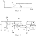
- the power supply control apparatus 110 of Figure 5 differs from the power supply control apparatus 10 of Figure 1 in that, in the power supply control apparatus 110 of Figure 5 , the power supply sequencer circuit includes first and second power supply sequencer stages 116, 216, instead of the single power supply sequencer stage 16 shown in Figure 1 .
Landscapes
- Power Conversion In General (AREA)
Priority Applications (3)
| Application Number | Priority Date | Filing Date | Title |
|---|---|---|---|
| EP18156059.0A EP3525331B1 (fr) | 2018-02-09 | 2018-02-09 | Appareil de régulation d'alimentation électrique |
| CA3032135A CA3032135A1 (fr) | 2018-02-09 | 2019-01-31 | Appareil de controle d'alimentation electrique |
| US16/270,973 US10812065B2 (en) | 2018-02-09 | 2019-02-08 | Power supply control apparatus |
Applications Claiming Priority (1)
| Application Number | Priority Date | Filing Date | Title |
|---|---|---|---|
| EP18156059.0A EP3525331B1 (fr) | 2018-02-09 | 2018-02-09 | Appareil de régulation d'alimentation électrique |
Publications (2)
| Publication Number | Publication Date |
|---|---|
| EP3525331A1 true EP3525331A1 (fr) | 2019-08-14 |
| EP3525331B1 EP3525331B1 (fr) | 2020-07-15 |
Family
ID=61189334
Family Applications (1)
| Application Number | Title | Priority Date | Filing Date |
|---|---|---|---|
| EP18156059.0A Active EP3525331B1 (fr) | 2018-02-09 | 2018-02-09 | Appareil de régulation d'alimentation électrique |
Country Status (3)
| Country | Link |
|---|---|
| US (1) | US10812065B2 (fr) |
| EP (1) | EP3525331B1 (fr) |
| CA (1) | CA3032135A1 (fr) |
Cited By (1)
| Publication number | Priority date | Publication date | Assignee | Title |
|---|---|---|---|---|
| CN114460834A (zh) * | 2021-12-24 | 2022-05-10 | 东莞市李群自动化技术有限公司 | 电源装置、自动控制设备及控制方法 |
Families Citing this family (1)
| Publication number | Priority date | Publication date | Assignee | Title |
|---|---|---|---|---|
| US12386406B2 (en) * | 2023-06-29 | 2025-08-12 | Semiconductor Components Industries, Llc | Power supply system for detecting a rail violation in a multi-rail sequence |
Citations (4)
| Publication number | Priority date | Publication date | Assignee | Title |
|---|---|---|---|---|
| JPS6148218A (ja) * | 1984-08-15 | 1986-03-08 | Makoto Aso | 遅延回路 |
| JPS6345914A (ja) * | 1986-08-13 | 1988-02-26 | Fujitsu Ltd | 可変遅延回路 |
| US20070257727A1 (en) * | 2006-04-26 | 2007-11-08 | Goh Ban H | Voltage detection and sequencing circuit |
| US20130307501A1 (en) * | 2012-05-16 | 2013-11-21 | Petr Kadanka | Method of forming a power supply controller and structure therefor |
Family Cites Families (4)
| Publication number | Priority date | Publication date | Assignee | Title |
|---|---|---|---|---|
| US5763960A (en) * | 1997-02-27 | 1998-06-09 | International Business Machines Corporation | Power supply controlled operation sequencing method and apparatus |
| US6850048B2 (en) * | 2003-05-02 | 2005-02-01 | Potentia Semiconductor, Inc. | Power supply controller |
| US7458028B2 (en) * | 2003-07-18 | 2008-11-25 | Avinash Chidambaram | Graphical interface for configuring a power supply controller |
| US10600384B2 (en) * | 2014-05-14 | 2020-03-24 | Barco Nv | Energy efficient power sequencer control circuit |
-
2018
- 2018-02-09 EP EP18156059.0A patent/EP3525331B1/fr active Active
-
2019
- 2019-01-31 CA CA3032135A patent/CA3032135A1/fr active Pending
- 2019-02-08 US US16/270,973 patent/US10812065B2/en active Active
Patent Citations (4)
| Publication number | Priority date | Publication date | Assignee | Title |
|---|---|---|---|---|
| JPS6148218A (ja) * | 1984-08-15 | 1986-03-08 | Makoto Aso | 遅延回路 |
| JPS6345914A (ja) * | 1986-08-13 | 1988-02-26 | Fujitsu Ltd | 可変遅延回路 |
| US20070257727A1 (en) * | 2006-04-26 | 2007-11-08 | Goh Ban H | Voltage detection and sequencing circuit |
| US20130307501A1 (en) * | 2012-05-16 | 2013-11-21 | Petr Kadanka | Method of forming a power supply controller and structure therefor |
Cited By (1)
| Publication number | Priority date | Publication date | Assignee | Title |
|---|---|---|---|---|
| CN114460834A (zh) * | 2021-12-24 | 2022-05-10 | 东莞市李群自动化技术有限公司 | 电源装置、自动控制设备及控制方法 |
Also Published As
| Publication number | Publication date |
|---|---|
| EP3525331B1 (fr) | 2020-07-15 |
| US20190253049A1 (en) | 2019-08-15 |
| CA3032135A1 (fr) | 2019-08-09 |
| US10812065B2 (en) | 2020-10-20 |
Similar Documents
| Publication | Publication Date | Title |
|---|---|---|
| US9628067B2 (en) | Gate driver | |
| CN105553235B (zh) | 半导体驱动装置及使用该半导体驱动装置的电力变换装置 | |
| CN101505055B (zh) | 有源浪涌电流控制电路 | |
| US20140177306A1 (en) | Method for operating an electrical power rectifier, as well as an electrical power rectifier | |
| US10812065B2 (en) | Power supply control apparatus | |
| JP5673634B2 (ja) | 駆動対象スイッチング素子の駆動回路 | |
| CN107706906A (zh) | 防倒灌电路及电源冗余电路 | |
| JP2016072676A (ja) | 半導体リレー | |
| JP6274099B2 (ja) | 信号出力回路 | |
| CN114553028B (zh) | 电压转换器 | |
| JP5834462B2 (ja) | 負荷駆動装置 | |
| KR101659088B1 (ko) | Led 전원 장치 | |
| CN103828205B (zh) | 用于控制电力开关的电源 | |
| DE2506894B2 (de) | Wechselstromlastschaltanordnung | |
| CN109565272B (zh) | 功率半导体电路 | |
| KR20190126080A (ko) | 전력 스위칭 장치 및 상기 전력 스위칭 장치를 동작시키는 방법 | |
| JP3713795B2 (ja) | 制御装置の出力回路 | |
| JP2017060250A (ja) | 漏電検出装置 | |
| CN112448703A (zh) | 开关装置 | |
| US20210273638A1 (en) | Universal semiconductor switch | |
| CN105430794B (zh) | 驱动芯片、led恒流驱动控制电路及led驱动方法 | |
| JP2023161485A (ja) | 点灯装置、及び照明装置 | |
| JP2020017003A (ja) | 電源ユニット、及び電源 | |
| JP6242004B2 (ja) | スイッチング電源装置 | |
| KR101764467B1 (ko) | 전류 제한 장치 |
Legal Events
| Date | Code | Title | Description |
|---|---|---|---|
| PUAI | Public reference made under article 153(3) epc to a published international application that has entered the european phase |
Free format text: ORIGINAL CODE: 0009012 |
|
| STAA | Information on the status of an ep patent application or granted ep patent |
Free format text: STATUS: THE APPLICATION HAS BEEN PUBLISHED |
|
| AK | Designated contracting states |
Kind code of ref document: A1 Designated state(s): AL AT BE BG CH CY CZ DE DK EE ES FI FR GB GR HR HU IE IS IT LI LT LU LV MC MK MT NL NO PL PT RO RS SE SI SK SM TR |
|
| AX | Request for extension of the european patent |
Extension state: BA ME |
|
| STAA | Information on the status of an ep patent application or granted ep patent |
Free format text: STATUS: REQUEST FOR EXAMINATION WAS MADE |
|
| REG | Reference to a national code |
Ref country code: DE Ref legal event code: R079 Ref document number: 602018005951 Country of ref document: DE Free format text: PREVIOUS MAIN CLASS: H02M0001080000 Ipc: H03K0017220000 |
|
| 17P | Request for examination filed |
Effective date: 20191219 |
|
| RBV | Designated contracting states (corrected) |
Designated state(s): AL AT BE BG CH CY CZ DE DK EE ES FI FR GB GR HR HU IE IS IT LI LT LU LV MC MK MT NL NO PL PT RO RS SE SI SK SM TR |
|
| GRAP | Despatch of communication of intention to grant a patent |
Free format text: ORIGINAL CODE: EPIDOSNIGR1 |
|
| STAA | Information on the status of an ep patent application or granted ep patent |
Free format text: STATUS: GRANT OF PATENT IS INTENDED |
|
| RIC1 | Information provided on ipc code assigned before grant |
Ipc: H03K 17/22 20060101AFI20200122BHEP Ipc: H03K 17/284 20060101ALI20200122BHEP Ipc: H02M 1/36 20070101ALN20200122BHEP |
|
| INTG | Intention to grant announced |
Effective date: 20200217 |
|
| GRAS | Grant fee paid |
Free format text: ORIGINAL CODE: EPIDOSNIGR3 |
|
| GRAA | (expected) grant |
Free format text: ORIGINAL CODE: 0009210 |
|
| STAA | Information on the status of an ep patent application or granted ep patent |
Free format text: STATUS: THE PATENT HAS BEEN GRANTED |
|
| AK | Designated contracting states |
Kind code of ref document: B1 Designated state(s): AL AT BE BG CH CY CZ DE DK EE ES FI FR GB GR HR HU IE IS IT LI LT LU LV MC MK MT NL NO PL PT RO RS SE SI SK SM TR |
|
| REG | Reference to a national code |
Ref country code: GB Ref legal event code: FG4D Ref country code: CH Ref legal event code: EP |
|
| REG | Reference to a national code |
Ref country code: DE Ref legal event code: R096 Ref document number: 602018005951 Country of ref document: DE |
|
| REG | Reference to a national code |
Ref country code: IE Ref legal event code: FG4D |
|
| REG | Reference to a national code |
Ref country code: AT Ref legal event code: REF Ref document number: 1292109 Country of ref document: AT Kind code of ref document: T Effective date: 20200815 |
|
| REG | Reference to a national code |
Ref country code: SE Ref legal event code: TRGR |
|
| REG | Reference to a national code |
Ref country code: LT Ref legal event code: MG4D |
|
| REG | Reference to a national code |
Ref country code: AT Ref legal event code: MK05 Ref document number: 1292109 Country of ref document: AT Kind code of ref document: T Effective date: 20200715 |
|
| REG | Reference to a national code |
Ref country code: NL Ref legal event code: MP Effective date: 20200715 |
|
| PG25 | Lapsed in a contracting state [announced via postgrant information from national office to epo] |
Ref country code: HR Free format text: LAPSE BECAUSE OF FAILURE TO SUBMIT A TRANSLATION OF THE DESCRIPTION OR TO PAY THE FEE WITHIN THE PRESCRIBED TIME-LIMIT Effective date: 20200715 Ref country code: FI Free format text: LAPSE BECAUSE OF FAILURE TO SUBMIT A TRANSLATION OF THE DESCRIPTION OR TO PAY THE FEE WITHIN THE PRESCRIBED TIME-LIMIT Effective date: 20200715 Ref country code: PT Free format text: LAPSE BECAUSE OF FAILURE TO SUBMIT A TRANSLATION OF THE DESCRIPTION OR TO PAY THE FEE WITHIN THE PRESCRIBED TIME-LIMIT Effective date: 20201116 Ref country code: BG Free format text: LAPSE BECAUSE OF FAILURE TO SUBMIT A TRANSLATION OF THE DESCRIPTION OR TO PAY THE FEE WITHIN THE PRESCRIBED TIME-LIMIT Effective date: 20201015 Ref country code: LT Free format text: LAPSE BECAUSE OF FAILURE TO SUBMIT A TRANSLATION OF THE DESCRIPTION OR TO PAY THE FEE WITHIN THE PRESCRIBED TIME-LIMIT Effective date: 20200715 Ref country code: NO Free format text: LAPSE BECAUSE OF FAILURE TO SUBMIT A TRANSLATION OF THE DESCRIPTION OR TO PAY THE FEE WITHIN THE PRESCRIBED TIME-LIMIT Effective date: 20201015 Ref country code: AT Free format text: LAPSE BECAUSE OF FAILURE TO SUBMIT A TRANSLATION OF THE DESCRIPTION OR TO PAY THE FEE WITHIN THE PRESCRIBED TIME-LIMIT Effective date: 20200715 Ref country code: GR Free format text: LAPSE BECAUSE OF FAILURE TO SUBMIT A TRANSLATION OF THE DESCRIPTION OR TO PAY THE FEE WITHIN THE PRESCRIBED TIME-LIMIT Effective date: 20201016 Ref country code: ES Free format text: LAPSE BECAUSE OF FAILURE TO SUBMIT A TRANSLATION OF THE DESCRIPTION OR TO PAY THE FEE WITHIN THE PRESCRIBED TIME-LIMIT Effective date: 20200715 |
|
| PG25 | Lapsed in a contracting state [announced via postgrant information from national office to epo] |
Ref country code: IS Free format text: LAPSE BECAUSE OF FAILURE TO SUBMIT A TRANSLATION OF THE DESCRIPTION OR TO PAY THE FEE WITHIN THE PRESCRIBED TIME-LIMIT Effective date: 20201115 Ref country code: PL Free format text: LAPSE BECAUSE OF FAILURE TO SUBMIT A TRANSLATION OF THE DESCRIPTION OR TO PAY THE FEE WITHIN THE PRESCRIBED TIME-LIMIT Effective date: 20200715 Ref country code: RS Free format text: LAPSE BECAUSE OF FAILURE TO SUBMIT A TRANSLATION OF THE DESCRIPTION OR TO PAY THE FEE WITHIN THE PRESCRIBED TIME-LIMIT Effective date: 20200715 Ref country code: LV Free format text: LAPSE BECAUSE OF FAILURE TO SUBMIT A TRANSLATION OF THE DESCRIPTION OR TO PAY THE FEE WITHIN THE PRESCRIBED TIME-LIMIT Effective date: 20200715 |
|
| PG25 | Lapsed in a contracting state [announced via postgrant information from national office to epo] |
Ref country code: NL Free format text: LAPSE BECAUSE OF FAILURE TO SUBMIT A TRANSLATION OF THE DESCRIPTION OR TO PAY THE FEE WITHIN THE PRESCRIBED TIME-LIMIT Effective date: 20200715 |
|
| REG | Reference to a national code |
Ref country code: DE Ref legal event code: R097 Ref document number: 602018005951 Country of ref document: DE |
|
| PG25 | Lapsed in a contracting state [announced via postgrant information from national office to epo] |
Ref country code: EE Free format text: LAPSE BECAUSE OF FAILURE TO SUBMIT A TRANSLATION OF THE DESCRIPTION OR TO PAY THE FEE WITHIN THE PRESCRIBED TIME-LIMIT Effective date: 20200715 Ref country code: RO Free format text: LAPSE BECAUSE OF FAILURE TO SUBMIT A TRANSLATION OF THE DESCRIPTION OR TO PAY THE FEE WITHIN THE PRESCRIBED TIME-LIMIT Effective date: 20200715 Ref country code: CZ Free format text: LAPSE BECAUSE OF FAILURE TO SUBMIT A TRANSLATION OF THE DESCRIPTION OR TO PAY THE FEE WITHIN THE PRESCRIBED TIME-LIMIT Effective date: 20200715 Ref country code: DK Free format text: LAPSE BECAUSE OF FAILURE TO SUBMIT A TRANSLATION OF THE DESCRIPTION OR TO PAY THE FEE WITHIN THE PRESCRIBED TIME-LIMIT Effective date: 20200715 Ref country code: IT Free format text: LAPSE BECAUSE OF FAILURE TO SUBMIT A TRANSLATION OF THE DESCRIPTION OR TO PAY THE FEE WITHIN THE PRESCRIBED TIME-LIMIT Effective date: 20200715 Ref country code: SM Free format text: LAPSE BECAUSE OF FAILURE TO SUBMIT A TRANSLATION OF THE DESCRIPTION OR TO PAY THE FEE WITHIN THE PRESCRIBED TIME-LIMIT Effective date: 20200715 |
|
| PLBE | No opposition filed within time limit |
Free format text: ORIGINAL CODE: 0009261 |
|
| STAA | Information on the status of an ep patent application or granted ep patent |
Free format text: STATUS: NO OPPOSITION FILED WITHIN TIME LIMIT |
|
| PG25 | Lapsed in a contracting state [announced via postgrant information from national office to epo] |
Ref country code: AL Free format text: LAPSE BECAUSE OF FAILURE TO SUBMIT A TRANSLATION OF THE DESCRIPTION OR TO PAY THE FEE WITHIN THE PRESCRIBED TIME-LIMIT Effective date: 20200715 |
|
| 26N | No opposition filed |
Effective date: 20210416 |
|
| PG25 | Lapsed in a contracting state [announced via postgrant information from national office to epo] |
Ref country code: SK Free format text: LAPSE BECAUSE OF FAILURE TO SUBMIT A TRANSLATION OF THE DESCRIPTION OR TO PAY THE FEE WITHIN THE PRESCRIBED TIME-LIMIT Effective date: 20200715 |
|
| PG25 | Lapsed in a contracting state [announced via postgrant information from national office to epo] |
Ref country code: SI Free format text: LAPSE BECAUSE OF FAILURE TO SUBMIT A TRANSLATION OF THE DESCRIPTION OR TO PAY THE FEE WITHIN THE PRESCRIBED TIME-LIMIT Effective date: 20200715 |
|
| PG25 | Lapsed in a contracting state [announced via postgrant information from national office to epo] |
Ref country code: MC Free format text: LAPSE BECAUSE OF FAILURE TO SUBMIT A TRANSLATION OF THE DESCRIPTION OR TO PAY THE FEE WITHIN THE PRESCRIBED TIME-LIMIT Effective date: 20200715 |
|
| REG | Reference to a national code |
Ref country code: BE Ref legal event code: MM Effective date: 20210228 |
|
| PG25 | Lapsed in a contracting state [announced via postgrant information from national office to epo] |
Ref country code: LI Free format text: LAPSE BECAUSE OF NON-PAYMENT OF DUE FEES Effective date: 20210228 Ref country code: LU Free format text: LAPSE BECAUSE OF NON-PAYMENT OF DUE FEES Effective date: 20210209 Ref country code: CH Free format text: LAPSE BECAUSE OF NON-PAYMENT OF DUE FEES Effective date: 20210228 |
|
| PG25 | Lapsed in a contracting state [announced via postgrant information from national office to epo] |
Ref country code: IE Free format text: LAPSE BECAUSE OF NON-PAYMENT OF DUE FEES Effective date: 20210209 |
|
| PG25 | Lapsed in a contracting state [announced via postgrant information from national office to epo] |
Ref country code: BE Free format text: LAPSE BECAUSE OF NON-PAYMENT OF DUE FEES Effective date: 20210228 |
|
| P01 | Opt-out of the competence of the unified patent court (upc) registered |
Effective date: 20230522 |
|
| PG25 | Lapsed in a contracting state [announced via postgrant information from national office to epo] |
Ref country code: CY Free format text: LAPSE BECAUSE OF FAILURE TO SUBMIT A TRANSLATION OF THE DESCRIPTION OR TO PAY THE FEE WITHIN THE PRESCRIBED TIME-LIMIT Effective date: 20200715 |
|
| PG25 | Lapsed in a contracting state [announced via postgrant information from national office to epo] |
Ref country code: HU Free format text: LAPSE BECAUSE OF FAILURE TO SUBMIT A TRANSLATION OF THE DESCRIPTION OR TO PAY THE FEE WITHIN THE PRESCRIBED TIME-LIMIT; INVALID AB INITIO Effective date: 20180209 |
|
| PG25 | Lapsed in a contracting state [announced via postgrant information from national office to epo] |
Ref country code: MK Free format text: LAPSE BECAUSE OF FAILURE TO SUBMIT A TRANSLATION OF THE DESCRIPTION OR TO PAY THE FEE WITHIN THE PRESCRIBED TIME-LIMIT Effective date: 20200715 |
|
| PGFP | Annual fee paid to national office [announced via postgrant information from national office to epo] |
Ref country code: DE Payment date: 20240123 Year of fee payment: 7 |
|
| PGFP | Annual fee paid to national office [announced via postgrant information from national office to epo] |
Ref country code: SE Payment date: 20240123 Year of fee payment: 7 |
|
| PG25 | Lapsed in a contracting state [announced via postgrant information from national office to epo] |
Ref country code: MT Free format text: LAPSE BECAUSE OF FAILURE TO SUBMIT A TRANSLATION OF THE DESCRIPTION OR TO PAY THE FEE WITHIN THE PRESCRIBED TIME-LIMIT Effective date: 20200715 |
|
| PGFP | Annual fee paid to national office [announced via postgrant information from national office to epo] |
Ref country code: FR Payment date: 20250122 Year of fee payment: 8 |
|
| PGFP | Annual fee paid to national office [announced via postgrant information from national office to epo] |
Ref country code: GB Payment date: 20250123 Year of fee payment: 8 |
|
| REG | Reference to a national code |
Ref country code: DE Ref legal event code: R119 Ref document number: 602018005951 Country of ref document: DE |
|
| REG | Reference to a national code |
Ref country code: SE Ref legal event code: EUG |
|
| PG25 | Lapsed in a contracting state [announced via postgrant information from national office to epo] |
Ref country code: TR Free format text: LAPSE BECAUSE OF FAILURE TO SUBMIT A TRANSLATION OF THE DESCRIPTION OR TO PAY THE FEE WITHIN THE PRESCRIBED TIME-LIMIT Effective date: 20200715 |
|
| PG25 | Lapsed in a contracting state [announced via postgrant information from national office to epo] |
Ref country code: DE Free format text: LAPSE BECAUSE OF NON-PAYMENT OF DUE FEES Effective date: 20250902 |