EP3528237B1 - Techniques de correction en courant pour source de courant de precision a haute intensite et a canal court - Google Patents
Techniques de correction en courant pour source de courant de precision a haute intensite et a canal court Download PDFInfo
- Publication number
- EP3528237B1 EP3528237B1 EP19157716.2A EP19157716A EP3528237B1 EP 3528237 B1 EP3528237 B1 EP 3528237B1 EP 19157716 A EP19157716 A EP 19157716A EP 3528237 B1 EP3528237 B1 EP 3528237B1
- Authority
- EP
- European Patent Office
- Prior art keywords
- current
- node
- terminal
- output
- transistor
- Prior art date
- Legal status (The legal status is an assumption and is not a legal conclusion. Google has not performed a legal analysis and makes no representation as to the accuracy of the status listed.)
- Active
Links
Images


Classifications
-
- G—PHYSICS
- G05—CONTROLLING; REGULATING
- G05F—SYSTEMS FOR REGULATING ELECTRIC OR MAGNETIC VARIABLES
- G05F3/00—Non-retroactive systems for regulating electric variables by using an uncontrolled element, or an uncontrolled combination of elements, such element or such combination having self-regulating properties
- G05F3/02—Regulating voltage or current
- G05F3/08—Regulating voltage or current wherein the variable is DC
- G05F3/10—Regulating voltage or current wherein the variable is DC using uncontrolled devices with non-linear characteristics
- G05F3/16—Regulating voltage or current wherein the variable is DC using uncontrolled devices with non-linear characteristics being semiconductor devices
- G05F3/20—Regulating voltage or current wherein the variable is DC using uncontrolled devices with non-linear characteristics being semiconductor devices using diode- transistor combinations
- G05F3/24—Regulating voltage or current wherein the variable is DC using uncontrolled devices with non-linear characteristics being semiconductor devices using diode- transistor combinations wherein the transistors are of the field-effect type only
-
- H—ELECTRICITY
- H05—ELECTRIC TECHNIQUES NOT OTHERWISE PROVIDED FOR
- H05B—ELECTRIC HEATING; ELECTRIC LIGHT SOURCES NOT OTHERWISE PROVIDED FOR; CIRCUIT ARRANGEMENTS FOR ELECTRIC LIGHT SOURCES, IN GENERAL
- H05B45/00—Circuit arrangements for operating light-emitting diodes [LED]
- H05B45/30—Driver circuits
-
- G—PHYSICS
- G05—CONTROLLING; REGULATING
- G05F—SYSTEMS FOR REGULATING ELECTRIC OR MAGNETIC VARIABLES
- G05F3/00—Non-retroactive systems for regulating electric variables by using an uncontrolled element, or an uncontrolled combination of elements, such element or such combination having self-regulating properties
- G05F3/02—Regulating voltage or current
- G05F3/08—Regulating voltage or current wherein the variable is DC
- G05F3/10—Regulating voltage or current wherein the variable is DC using uncontrolled devices with non-linear characteristics
- G05F3/16—Regulating voltage or current wherein the variable is DC using uncontrolled devices with non-linear characteristics being semiconductor devices
- G05F3/20—Regulating voltage or current wherein the variable is DC using uncontrolled devices with non-linear characteristics being semiconductor devices using diode- transistor combinations
- G05F3/26—Current mirrors
- G05F3/262—Current mirrors using field-effect transistors only
-
- G—PHYSICS
- G09—EDUCATION; CRYPTOGRAPHY; DISPLAY; ADVERTISING; SEALS
- G09G—ARRANGEMENTS OR CIRCUITS FOR CONTROL OF INDICATING DEVICES USING STATIC MEANS TO PRESENT VARIABLE INFORMATION
- G09G3/00—Control arrangements or circuits, of interest only in connection with visual indicators other than cathode-ray tubes
- G09G3/04—Control arrangements or circuits, of interest only in connection with visual indicators other than cathode-ray tubes for presentation of a single character by selection from a plurality of characters, or by composing the character by combination of individual elements, e.g. segments using a combination of such display devices for composing words, rows or the like, in a frame with fixed character positions
- G09G3/06—Control arrangements or circuits, of interest only in connection with visual indicators other than cathode-ray tubes for presentation of a single character by selection from a plurality of characters, or by composing the character by combination of individual elements, e.g. segments using a combination of such display devices for composing words, rows or the like, in a frame with fixed character positions using controlled light sources
- G09G3/12—Control arrangements or circuits, of interest only in connection with visual indicators other than cathode-ray tubes for presentation of a single character by selection from a plurality of characters, or by composing the character by combination of individual elements, e.g. segments using a combination of such display devices for composing words, rows or the like, in a frame with fixed character positions using controlled light sources using electroluminescent elements
- G09G3/14—Semiconductor devices, e.g. diodes
-
- H—ELECTRICITY
- H05—ELECTRIC TECHNIQUES NOT OTHERWISE PROVIDED FOR
- H05B—ELECTRIC HEATING; ELECTRIC LIGHT SOURCES NOT OTHERWISE PROVIDED FOR; CIRCUIT ARRANGEMENTS FOR ELECTRIC LIGHT SOURCES, IN GENERAL
- H05B45/00—Circuit arrangements for operating light-emitting diodes [LED]
- H05B45/10—Controlling the intensity of the light
-
- H—ELECTRICITY
- H05—ELECTRIC TECHNIQUES NOT OTHERWISE PROVIDED FOR
- H05B—ELECTRIC HEATING; ELECTRIC LIGHT SOURCES NOT OTHERWISE PROVIDED FOR; CIRCUIT ARRANGEMENTS FOR ELECTRIC LIGHT SOURCES, IN GENERAL
- H05B45/00—Circuit arrangements for operating light-emitting diodes [LED]
- H05B45/30—Driver circuits
- H05B45/345—Current stabilisation; Maintaining constant current
-
- H—ELECTRICITY
- H05—ELECTRIC TECHNIQUES NOT OTHERWISE PROVIDED FOR
- H05B—ELECTRIC HEATING; ELECTRIC LIGHT SOURCES NOT OTHERWISE PROVIDED FOR; CIRCUIT ARRANGEMENTS FOR ELECTRIC LIGHT SOURCES, IN GENERAL
- H05B45/00—Circuit arrangements for operating light-emitting diodes [LED]
- H05B45/30—Driver circuits
- H05B45/395—Linear regulators
- H05B45/397—Current mirror circuits
-
- Y—GENERAL TAGGING OF NEW TECHNOLOGICAL DEVELOPMENTS; GENERAL TAGGING OF CROSS-SECTIONAL TECHNOLOGIES SPANNING OVER SEVERAL SECTIONS OF THE IPC; TECHNICAL SUBJECTS COVERED BY FORMER USPC CROSS-REFERENCE ART COLLECTIONS [XRACs] AND DIGESTS
- Y02—TECHNOLOGIES OR APPLICATIONS FOR MITIGATION OR ADAPTATION AGAINST CLIMATE CHANGE
- Y02B—CLIMATE CHANGE MITIGATION TECHNOLOGIES RELATED TO BUILDINGS, e.g. HOUSING, HOUSE APPLIANCES OR RELATED END-USER APPLICATIONS
- Y02B20/00—Energy efficient lighting technologies, e.g. halogen lamps or gas discharge lamps
- Y02B20/30—Semiconductor lamps, e.g. solid state lamps [SSL] light emitting diodes [LED] or organic LED [OLED]
Definitions
- the present disclosure relates generally tocurrent driver circuitry, and more particularly to controlling current flow in current driver applications.
- a current driver is employed to control current flow through a diode, such as a Light Emitting Diode (LED).
- a remote control includes a microcontroller, the current driver, the LED, and abattery that supplies a Direct Current (DC) voltage onto a supply node.
- DC Direct Current
- One terminal of the LED is coupled to the supply node and another terminal of the LED is coupled in some fashion to the current driver.
- the current driver controls an output current that flows through the LED, either by sourcing current from the battery, through the current driver, through the LED and onto a ground node, or by sinking current from the supply node, through the LED, through the current driver, and onto the ground node.
- the current driver uses a reference current to set a current level of the output current through the LED. The current level of the output current is generally desired to be maintained at a pre- determined multiple of the reference current.
- US 2012/228934 A1 refers to 'A multi-current-source comprises a voltage converter (VC), a first current source (CS1) with a first terminal (A1) which is adapted to be coupled to an output (OUT) of a voltage converter (VC) and with a second terminal (B1) which is adapted to be coupled to an input (IN) of the voltage converter (VC), at least a second current source (CS2) with a first terminal (A2) which is adapted to be coupled to the output (OUT) of the voltage converter (VC) and with a second terminal (B2) which is adapted to be coupled to the input (IN) of the voltage converter (VC), wherein the first current source (CS1) being adapted to provide a first load current (111) at its first terminal (A1) the first load current (111) being regulated to a first constant value and to provide a first unidirectional error current (Ierr1) at its second terminal (B1), wherein the at least one second current source (CS2) being adapted to provide a second load current (112)
- WO 03/102708 A2 refers to 'A voltage regulator with dynamically boosted bias current includes a pass device for providing current to a load; an error circuit responsive to a difference between a predetermined reference voltage and a function of the voltage on the load to produce an error signal, a driver circuit responsive to the error signal for controlling the pass device to adjust the current to the load to reduce the error signal, the driver circuit including an amplifier responsive to the error signal for controlling the pass device, a bias current source for biasing the amplifier, a sensing circuit for sensing a portion of the error signal, a reference current source for providing a reference current, a second error circuit responsive to a difference between the portion of the error signal and the reference current to produce a second error current; and a boost circuit responsive to the second error signal to increase the bias current provided to the amplifier when the load demands more current.
- US 2005/099748 A1 refers to ' a dual stage power supply with a protection circuit for preventing reverse conduction through the lower voltage driver of the dual stage power supply and excess power dissipation when the higher voltage driver is on.
- the protection scheme comprises a comparator that detects when the voltage on the output pad exceeds a predetermined voltage and a protection transistor which is controlled by the comparator to block reverse conduction through the lower voltage driver when the higher voltage driver is operating.
- US 6433528 B1 refers to 'A high-impedance current source 100 having an enhanced compliance voltage.
- the current source 100 preferably has a means for generating a biasing current 105 and a first current mirror stage having a first transistor M6 coupled to a second transistor M1.
- a second current mirror stage having a third transistor M2 coupled to a fourth transistor M5 acts as a feedback circuit.
- a stabilization circuit having a fifth transistor M3 coupled to a sixth transistor M4 are also included.
- the stabilization circuit is coupled between the first and second current mirror stages and an output circuit having a seventh transistor M7 is connected to the stabilization circuit between the first and second current mirror stages.
- the current mirror circuit has a low compliance voltage, enhanced operating characteristics and enhanced dynamics which eliminate the need for OTAs.'
- a system comprises a supply node, a controller integrated circuit (IC), a current driver IC, a diode, and a ground node.
- the current driver IC is an example of a high current driver that controls currents greater than at least 200 milliamps through the diode.
- the diode is a Light Emitting Diode (LED) and the current driver IC is coupled to sink current from the supply node, through the diode, through the current driver IC, and onto the ground node.
- the LED has an anode coupled to a supply node and a cathode coupled to a drive terminal of the current driver IC.
- the current driver has a control terminal coupled to receive a control signal EN from the controller IC that enables (turning on the LED) ordisables (turning off the LED) the currentdriver IC.
- the supply node is supplied by Direct Current (DC) source such as a battery.
- the supply node is supplied by an Alternating Current (AC) source, such as an AC line.
- DC Direct Current
- AC Alternating Current
- the current driver IC is enabled and sinks an output current from the supply node, through the LED, through the drive terminal, and onto a ground node.
- An output voltage is present between the cathode of the LED and the ground node.
- the output voltage typically varies due to charge and discharge cycles of the battery which cause the battery voltage to decrease over time.
- the output voltage may also vary depending on the voltage and current demands across different applications.
- changes in temperature of the LED may also cause the output voltage to change.
- the current driver IC maintains variation of a current level of the output current to be within five percent of a desired output current level when the output voltage is anywhere withinat least a two-volt range.
- the desired output current level is 250 milliamps
- the current driver IC controls the output current to be between 255 milliamps and 245 milliamps when the output voltage is anywhere between at least 0.3 volts and 2.4 volts.
- the current driver integrated circuit preferably comprises a voltage detector circuit, an Output Model Current Mirror (OMCM) circuit, a Corrected Current Mirror (CCM) circuit, a summing node reference current generator circuit, a Corrected Current to Gate Voltage Converter (CCGVC) circuit, a summing node, and a current drive transistor.
- the voltage detector circuit detects an output voltage on an output node and generates a replica voltage.
- the OMCM circuit receives the replica voltage and generates an output model current I s .
- the output model current I S models a short channel effect on the current driver transistor.
- the output model current I S is a factor of the reference current I REF modulated by the output voltage V OUT . In this example, the factor is approximately one.
- the short channel current modulation is caused by short channel effects present on a transistor of the OMCM circuit that is coupled to detect the replica voltage.
- the transistor of the OMCM circuit that detects the replica voltage has a drain terminal on which the replica voltage is present.
- the amount of modulation is adjustable by adjusting the length of the transistor that detects the replica voltage. The length of this transistor is adjusted to increase or decrease the amount of short channel current modulation to match that of the current driver transistor.
- the summing node can be maintained at a stable current level which is a first factor times a reference current. For example, a current on the summing node is maintained to be twice a reference current ("2 x I REF ").
- the OMCM circuit supplies the output model current I s onto the summing node, and the CCM circuit generates and supplies a corrected current I C onto the summing node. Because the current on the summing node is substantially constant, and because both the output model current I S and the corrected current I C are supplied onto the summing node, as the output model current I S decreases, the corrected current I C increases.
- a scaled corrected current I D is used to generate a gate voltage that controls operation of the current driver transistor.
- the CCM circuit generates the scaled corrected current I D by scaling the corrected current I C by a second factor. For example, the scaled corrected current I D is fifteen times the corrected current I C .
- the CCGVC circuit receives the scaled corrected current I D and converts the scaled corrected current I D into a gate voltage.
- the CCGVC circuit supplies the gate voltage onto a gate terminal of the current driver transistor.
- the gate voltage controls the conductivity of the current driver transistor such that current flow through the diode remains within five percent of the desired output current level over at least a 2V range of the output voltage.
- the desired output current level is a third factor times the scaled corrected current I D .
- the current level of the output current I OUT is two-hundred and six times the scaled corrected current I D .
- the increase in corrected current I C compensates for the decrease in output model current due to variation in the output voltage V OUT thereby controlling the current level of the output current I OUT to be maintained within five percent of the desired output current level.
- Figure 1 is a circuit diagram of a current driver circuit 10 having a single drive transistor 11.
- the current driver circuit 10 includes a reference current generator 12 and a current mirror circuit 13.
- the current mirror circuit includes the drive field effect transistor 11 and field effect transistor 14.
- a gate terminal of transistor 14 is coupled to a drain terminal of the transistor 14.
- the gate terminal of transistor 14 is also coupled to a gate terminal of the drive transistor 11.
- the drive transistor 11 is approximately two-hundred ("200") times the size of transistor 14.
- the current driver circuit 10 drives load 15 from supply node 16.
- a load 15 is coupled between a supply node 16 and a drain terminal of the drivetransistor 11.
- a source terminal of the drive transistor 11 is coupled to a ground node 17.
- the current driver circuit 10 drives the load 15 by sinking current I OUT 18 from a supply node 16 through the load 15 through the drive field effect transistor 11 and onto a ground node 17.
- the reference current generator circuit 12 outputs a reference current I REF 19 onto a drain terminal of the transistor 14.
- the output current I OUT 18 that flows through the load 15 is a factor of the reference current I REF 19.
- the factor is determined by a ratio of the size of the drive transistor 11 to the size of the transistor 14. In this example, the factor is two-hundred ("200") because the drive transistor 11 is approximately two-hundred ("200") times the size of transistor 14.
- the output current I OUT 18 will be 200 times the reference current I REF 19.
- the reference current I REF 19 is approximately 1.2 milliamps and the output current I OUT 18 will be approximately 240 milliamps.
- the output current I OUT 18 In most applications of current driver circuit 10, it is desirable for the output current I OUT 18 to remain constant and at a fixed factor of the reference current I REF 19 across a range of output voltage V OUT 20. However, during operation of the current driver circuit 10, the output current I OUT 18 tends to change as the output voltage V OUT 20 changes. As shown in Figure 3 , the output current I OUT 18 varies approximately 90 milliamps over a 2V range of output voltage 20.
- FIG 2 is a diagram of a top-down view of drive transistor 11 shown in Figure 1 .
- the drive transistor 11 includes a polysilicon gate 21, a drain region 22, and a source region 23.
- the variation of the output current I OUT 18 can be minimized by increasing length L of the polysilicon gate 21.
- increasing the length L requires increasing the width W to maintain the samewidth to length ratio of the drive transistor 11, which in turn, increases the overall size of drive transistor 11.
- Increasing the size of drive transistor 11 is generally undesirable due to increased die area that would be consumed by the drive transistor 11. For example, if the width W increases by a factor of two ("2”), then the length L would also be increased by a factor of two (“2”) to maintain the width to length ratio.
- an overall die area of the transistor would increase by a factor of four ("4").
- Figure 3 is a diagram showing graphs of the output current I out 18 and reference current I REF 19 versus the output voltage V OUT 20 during operation of the current driver circuit 10 shown in Figure 1 .
- the output voltage V out 20 extends approximately 2V ranging from 0.4 V to 2.4V.
- the reference current I REF 19 is set at a constant 1.2 milliamps over the range of output voltages.
- the output current extends from around 185 milliamps to approximately 275 milliamps over the range of output voltages.
- the current driver circuit 10 shown in Figure 1 has an output current 18 that varies approximately 90 milliamps over a 2.0V range of output voltages. As identified by dashed line 24, when the output voltage V out 20 is less than 0.6V, the output current I out 18 increases much more rapidly as compared to when the output voltage V OUT 20 is greaterthan 0.6 V.
- FIG. 4 is a circuit diagram of a current driver circuit 30 having two high power output transistors 31 and 32.
- Current driver circuit 30 comprises a reference current generator 33, the drive transistor 31, and the cascode transistor 32.
- a drain terminal of the cascode transistor 32 is coupled to load 35.
- a source terminal of the cascode transistor 32 is coupled to a drain terminal of the drive transistor 31.
- the current driver circuit 30 sinks an output current I OUT 36 from the supply node 37, through load 35, through cascodetransistor 32, through drive transistor 31, and onto a ground node38.
- the reference current generator 33 outputs a reference current I REF 39 onto a drain terminal of the transistor 34.
- the output current I OUT 36 is a factor of the reference current I REF 39.
- the factor depends upon a width to length ratio of the drive transistor 31 and a width to length ratio of transistor 34.
- An output voltage V OUT 40 is present between a drain terminal of the cascode transistor 32 and a source terminal of the drive transistor 31.
- the cascode transistor 32 and the drive transistor 31 are each two-hundred ("200") times a sizeof the transistor 34.
- Figure 5 is a diagram showing graphs of the output current I OUT 36 and reference current I REF 39 versus the output voltage V out 40 during operation of the current driver circuit 30 shown in Figure 4 .
- the output current I OUT 36 tends to vary depending on the output voltage V OUT 40. As identified by dashed line 41, when the output voltage V out 40 is less than 0.8V, the output current I out 36 increases much more rapidly as compared to when the output voltage V OUT 40 is greater than 0.8 V. Over a range of 2V of the output voltage V OUT 40, the current I OUT 36 of the current driver circuit 30 varies by approximately 100 milliamps.
- FIG. 6 is a circuit diagram of system 50 involving a novel current driver integrated circuit 51.
- System 50 comprises the current driver integrated circuit 51, a battery 52, a controller integrated circuit 53, a diode 54, a supply node 55, and a ground node 56.
- the battery 52 has a positive terminal that is coupled to the supply node 55, and a negative terminal that is coupled to the ground node 56.
- the battery 52 controls the supply node 55 to be at a fixed voltage VDD.
- VDD is between 2.7 V and 3.3 V.
- diode 54 is a light emitting diode (LED).
- system 50 is part of a remote control in which current is pulsed through the diode thereby radiating energy used in wireless communication.
- the controller integrated circuit 53 has a supply terminal 57, a control terminal 58, and a ground terminal 59.
- the supply terminal 57 of the controller integrated circuit 53 is coupled to the supply node 55.
- the ground terminal 59 of the controller integrated circuit 53 is coupled to the ground node 56.
- the current driver integrated circuit 51 has a supply terminal 60, a control terminal 61, a drive terminal 62, and a ground terminal63.
- the supply terminal 60 of the current driver integrated circuit 51 is coupled to the supply node 55.
- the ground terminal 63 of the current driver integrated circuit 51 is coupled to the ground node 56.
- the control terminal 61 of the current driver integrated circuit 51 is coupled to the control terminal 58 of the controller integrated circuit 53.
- the current driver IC 51 is an integrated circuit die and the terminals 60-63 are bond pads.
- Diode 54 has an anode terminal A that is coupled to the supply node 55.
- Diode 54 has a cathode terminal C that is coupled to the drive terminal 62 of the current driver integrated circuit 51.
- the controller integrated circuit 53 and current driver integrated circuit 51 are supplied by a direct current (DC) source, however, in other embodiments the controller integrated circuit 53 and the current driver integrated circuit 51 are supplied from an Alternating Current (AC) source.
- DC direct current
- AC Alternating Current
- the diode 54 is initially off and in a non-conductive state such that no current is flowing through diode 54.
- the controller integrated circuit 53 determines that the diode 54 is to switch from a non- conductive state to a conductive state such that current is to flow through the diode 54.
- Controller integrated circuit 53 asserts a control signal EN 64 that is supplied from the control terminal 58 onto the control terminal 61 of the current driver integrated circuit 51 via conductor 64.
- the current driver integrated circuit 51 sinks current from the supply node 55 through the diode 66, and onto the ground node 56 through the current driver integrated circuit 51.
- the current driver integrated circuit 51 drives the diode 54 such that the output current I OUT 66 varies by less than 10% over a range of output voltage V OUT 67.
- the battery voltage might start out at 3.6V and a typical voltage drop across the LED might be 1.2V, so the output voltage V OUT 67 would be 2.4V. If the battery discharges to 1.8V, then the output voltage V OUT 67 could decrease to 0.6V.
- the output current I OUT 66 remains within a desired output current range where the output voltage V OUT 67 ranges between 0.4V and 2.4V (or a 2V range).
- the current driver integrated circuit 51 drives the diode 54 such that the outputcurrent I OUT 66 varies by less than four percent over at least a two-volt range of output voltages V OUT 67. In another example, the current driver integrated circuit 51 drives the diode 54 such that the output current I OUT 66 varies by less than ten percent over at least a two-volt range of output voltages V OUT 67.
- FIG. 7 is a detailed circuit diagram of the current driver integrated circuit 51 shown in Figure 6 .
- the current driver integrated circuit 51 comprises voltage detector circuit 70, an Output Model Current Mirror (OMCM) circuit 71, a Corrected Current Mirror (CCM) circuit 72, a summing node reference current generator circuit 73, a Corrected Current To Gate Voltage Converter (CCGVC) circuit 74, a reference current generator 75, a bias current generator 76, a current drive transistor 77, an inverter 78, transistors 79, 80, 81 and 82, a replica node 83, an output node 84, a reference current node 85, a bias current node 86, and a summing node 87.
- the reference current generator 75 generates and outputs a reference current I REF 88 onto the reference current node 85.
- the bias current generator 76 generates and outputs a bias current I BIAS 89 on to the bias current node 86.
- the voltage detector circuit 70 detects the output voltage V OUT 67 on the output node 84 and generates a replica voltage 90.
- the voltage detector circuit 70 outputs the generated replica voltage 90 onto the replica node 83.
- the voltage detector circuit 70 comprises a first transistor 91 and a second transistor 92.
- a drain terminal and a gate terminal of first transistor 91 are coupled to the bias current node 86 and receives the bias current I BIAS 89.
- a source terminal of the first transistor 91 is coupled to the output node 84.
- a gate of the first transistor 91 is coupled to a gate of the second transistor 92.
- the detected output voltage V OUT 67 plus the voltage required to turn on the first transistor 91 is received onto the gate of the second transistor 92.
- a drain terminal of the second transistor 92 is coupled to the OMCM circuit 71 and a source terminal of the second transistor 92 is coupled to the replica node 83.
- the Output Model Current Mirror (OMCM) circuit 71 receives the replica voltage 90 generated by the voltage detector circuit 70 and generates an output model current I s 93.
- the output model current I S 93 is supplied onto the summing node 87.
- the output model current I S 93 is also referred to as a model short channel effect current because it models a short channel effect on the current driver transistor 77.
- the OMCM circuit 71 outputs the generated output model current I S 93 onto the summing node 87.
- the output model current I S 93 is a factor of the I REF current88 modulated by the output voltage V OUT 67. In this example, the factor is approximately one.
- the short channel current modulation is due to short channel effects present on transistor 94. The amount of modulation is adjusted by adjusting the length of transistor 94 to increase or decrease the amount of short channel current modulation to match that of current driver transistor 77.
- the OMCM circuit 71 comprises a first transistor 94, second transistor 95, and a third transistor 96.
- the second transistor 95 and the third transistor 96 form a current mirror.
- the gate of the second transistor 95 is coupled to the gate of the third transistor 96 and to a drain terminal of the second transistor 95.
- the gates of both the second transistor 95 and the third transistor 96 are coupled to a drain terminal of the second transistor 92 of the voltage detector circuit 70.
- Source terminals of the second transistor 95 and the third transistor 96 are coupled to the supply node 55 via the supply terminal 60.
- a drain terminal of the third transistor 96 is coupled to the summing node 87.
- the Corrected Current Mirror (CCM) circuit 72 generates a scaled corrected current 97.
- the CCM circuit 72 generates the scaled corrected current 97 by scaling a corrected current 98.
- the corrected current 98 is supplied onto the summing node 87.
- a summing node reference current 99 is present on the summing node 87.
- the summing node reference current 99 is fixed and independent of the supply voltage VDD.
- the summing node reference current 99 is a sum of the output model current I S 93 and the corrected current I C 98.
- the corrected current I C 98 is a difference between the summing node reference current 99 and the output model current I S 93.
- the CCM circuit 72 comprises a current mirrorthat includes a first transistor 100 and a second transistor 101.
- Source terminals of the first transistor 100 and the second transistor 101 are coupled to the supply node 55 via the supply terminal 60.
- Gates of the first transistor 100 and the second transistor 101 are coupled to the drain terminal of the first transistor 100 and to the summing node 87.
- a drain terminal of the second transistor 101 is coupled to a gate voltage node 102.
- the Corrected Current to Gate Voltage Converter (CCGVC) circuit 74 receives the scaled corrected current I D 97.
- the CCGVC circuit 74 converts the scaled corrected current I D 97 onto a gate voltage 103.
- the CCGVC circuit 74 supplies the generated gate voltage 103 onto a gate terminal of the current driver transistor 77.
- the gate voltage 103 is a function of the scaled corrected current I D 97.
- the gate voltage 103 controls the conductivity of the current driver transistor 77 and in turn, controls current flow through the diode 54.
- the CCGVC circuit 74 comprises a first transistor 104 and a second transistor 105.
- a drain terminal of the first transistor 104 is coupled to gate voltage node 102.
- a source terminal of the first transistor 104 is coupled to a drain terminal of the second transistor 105.
- a gate of the first transistor 104 is coupled to the bias current node 86 and to the gate of the first transistor 91 of the voltage detector circuit 70.
- a gate terminal of the second transistor 105 is coupled to the gate voltage node 102.
- a source terminal of the second transistor 105 is coupled to the ground node 56 via the ground terminal 63.
- the summing node reference current generator circuit 73 generates the summing node reference current 99 on the summing node 87.
- the reference current generator circuit 73 comprises a first transistor 106 and a second transistor 107.
- the summing node reference current generator circuit 73 maintains a current level of the summing node reference current 99 on the summing node 87 to be at a current level equal to the reference current I REF 88 times a firstfactor 108.
- the first factor is two ("2") and consequently the summing node reference current 99 is maintained to be twice the reference current I REF 88.
- the output model current I S 93 and corrected current I C 98 supplied onto the summing node 87 change in an opposite manner. For example, a decrease in the output model current 93 during the operating mode results in a corresponding increase in the corrected current I C 98. As the output voltage V OUT 67 decreases mainly due todischarge of battery 52, the output model current I S 93 tends to decrease. In response, the corrected current I C 98 increases thereby causing the output current 66 toremain within five percent of the desired output current overat least a 2V range of the output voltage 67.
- Figure 8 is a graph of current on various nodes versus the output voltage V OUT 67 during operation of the current driver integrated circuit 51 shown in Figure 7 .
- the desired current level of the output current I OUT 66 is approximately 250.0 milliamps. As shown in Figure 8 , the current level of the output current I OUT 66 remains within +/- 5.0 milliamps of the desired current level. Due to the novel control technique, the output current I OUT 66 varies less than +/- 2% of the desired current level when the output voltage V OUT 67 is between 0.3 volts and 2.4volts.
- the current driver integrated circuit 51 yields a substantially more stable output current as compared to the current driver 10 shown in Figure 1 and compared to the current driver 30 shown in Figure 4 .
- FIG 9 is a flowchart of a method 200 in accordance with one novel aspect.
- a summing node reference current is supplied onto a summing node of a currentdriver circuit.
- the summing node reference current 99 on the summing node 87 is maintained at a stable and constant current level by the summing node reference current generator circuit 73.
- the current level is a first factor 108 times the reference current I REF 88 (for example, "2 x I REF ").
- a second step an output voltage of a current driver circuit is detected during an operating mode.
- the output voltage is present on an output node of the current driver circuit.
- the output voltage V OUT 67 present between the output node 84 and the ground node 56 is detected by the voltage detector circuit 70.
- the voltage detector circuit 70 is a source follower circuit.
- a replica voltage is generated from the detected output voltage.
- the replica voltage is supplied onto a replica node.
- the voltage detector circuit 70 generates a replica voltage 90 that is supplied onto the replica node 83.
- the replica voltage 90 changes proportionally with respect to the output voltage V OUT 67.
- an output model current is generated using the replica voltage that is present on the replica node.
- the output model current is supplied onto a summing node.
- the OMCM circuit 71 receives the replica voltage 90 from the replica node 83 and generates therefrom an output model current I S 93.
- the OMCM circuit 71 supplies the generates output model current I S 93 onto the summing node 87.
- a corrected current is generated using the output model current and the summing node reference current.
- the corrected current is a difference between the summing node reference current and the output model current.
- the CCM circuit 72 generates a corrected current I C 98 that is supplied onto the summing node 87. Because the summing node 87 is maintained at the constant current level ("2 x I REF "), as the output model current I S 93 decreases, this causes the corrected current I C 98 to increase in a corresponding fashion.
- a gate voltage is generated and supplied onto a current driver transistor.
- the gate voltage is generated from a current proportional to the corrected current.
- the current driver transistor is part of the current driver circuit and has a terminal coupled to the output node.
- the CCM circuit 72 generates a scaled corrected current I D 97 and supplies the scaled corrected current I D 97 onto the CCGVC circuit 74.
- the scaled corrected current I D 97 has a current level that is a second factor 109 times the corrected current I C 98, for example "15 x I C ".
- the scaled corrected current I D 97 is proportional to the corrected current I C 98.
- the CCGVC circuit 74 receives the scaled corrected current I D 97 and generates therefrom a gate voltage 103 that is supplied onto the gate of the current driver transistor 77.
- the drain of the current driver transistor 77 is coupled to the output node 84 via the drive terminal 62.
- the gate voltage 103 controls the output current I OUT 66 to have a current level that is a third factor 110 times the scaled corrected current I D 97, for example "206 x I D ".
- Figure 10 is a table 300 showing the substantial improvement in stability and size of the output current that is achieved by the current driver 51 as compared to the current drivers 10 and 30.
- the variation of the current through the diode being driven by the current driver 51 is less than five percent when the outputvoltage is anywhere between 0.3 volts and 2.4 volts and significantly smaller in area than current driver 30.
- Figure 11 is a diagram showing how the gate voltage 103 is a function of the corrected current I C 98.
- the gate voltage 103 is supplied onto a gate of the current driver transistor 77 and controls current flow through the diode 54.
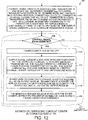
- FIG. 12 is a flowchart of a method 400 in accordance with another novel aspect.
- Method 400 is a method of operating the current driver circuit 51.
- a first step 401 identifies the state of various transistors of the current driver I C 51 before the control signal EN 64 is asserted and current is not conducting through the diode 54.
- Steps 402-406 identify a novel current control loop that maintains the output current within five percent of the desired output current level while current is conducting through the diode 54.
- a first step the control signal EN 64 is de-asserted and the transistors 79 and 80 are on.
- Reference current I REF 88 conducts through transistors 81 and 82.
- the summing node reference current 99 is flowing through transistors 106, 107, and 79.
- the transistor 79 maintains transistors 100 and 101 in a non-conductive state.
- Transistor 80 maintains transistors 104 and 105 of the CCGVC circuit 74 in a non-conductive state and transistor 80 also maintains current driver transistor 77 in a non-conductive state.
- Bias current 89 maintains transistor 91 in a conductive state.
- Transistor 92 maintains a voltage on the replica node 83 substantially equal to the output voltage V OUT 67 on the output node 84.
- the output model current I S 93 is flowing in transistors 95, 92, and 94.
- step 402 it is determined whether the control signal EN 64 is asserted. If the control signal EN 64 is de-asserted (for example, adigital logic low level), then the method proceeds to initial step 401. If, on the other hand, the control signal EN 64 is asserted (for example, a digital logic high level), then the method 400 proceeds to the steps of the currentcontrol loop 407.
- transistors 79 and 80 are switched from a conductive state to a non-conductive state.
- the control signal EN 64 is supplied onto the gate of the transistor 79 causing transistor 79 to switch off.
- Inverter 78 supplies an inverted version of the control signal EN 64 onto the gate of transistor 80 causing transistor 80 to switch off.
- Transistors 79 and 80 are of opposite conductivity types. For example, transistor 79 is P-type Field Effect Transistor (P-type FET) and transistor 80 is an N-type Field Effect Transistor (N-type FET).
- step 404 output model current I S 93 flows through transistor 96.
- the corrected current I C 98 flows through transistor 100.
- the scaled corrected current I D 97 flows through transistors 101, 104, and 105.
- the output current I OUT 66 flows through diode 54, through current driver transistor 77, and onto ground node 56.
- a fifth step in response to detecting a change in output voltage V OUT 67 on output node 84, transistors 91 and 92 cause the replica voltage 90 on the replica node 83 to match the output voltage V OUT 67 on the output node 84.
- step 406 the adjusted replica voltage 90 adjusts the short channel effect on transistor 93 which in turn adjusts other currents accordingly.
- the method proceeds to step 402 where it is determined whether to remain in the current control loop 407 if the control signal EN 64 is asserted, or to return to the initial step of 401 if the control signal EN 64 is de- asserted.
- the present invention has been described in connection with certain specific embodiments for instructional purposes, the present invention is not limited thereto.
- the current driver IC 51 of Figure 6 sinks current from the LED 54 to ground
- the current driver IC 51 is coupled between the supply node and the LED 54 such that the current driver IC 51 sources current from the supplynode 55 through the LED 54, and onto ground node 56.
- the example of Figure 6 uses a Direct Current (DC) voltage source 52 for supplying the LED 54.
- DC Direct Current
- AC Alternating Current
- a rectifier is used to rectify an AC voltage from the AC source.
- a switching regulator receives the rectified AC voltage and supplies a fixed DC voltage onto the supply node 55.
- the current driver IC 51 has only one control terminal 61 onto which the controller IC 53 supplies the control signal EN 64, in other examples, the current driver IC has more than one control terminal.
- the current driver 51 is configured to receive a current control signal.
- the current control indicates a desired output current to send through the LED 54.
- the current control signal is used by the current driver IC 51 to set the various currents of the control loop such that the output current I OUT 66 is at the desired current level indicated by the current control signal.
- the supply voltage VDD is between 2.7V and 3.3V and the output voltage V OUT extends approximately 2V. It is appreciated that these voltage ranges are but one example, and in other embodiments, the novel current driver IC 51 can be used with substantially higher voltages (greater than 12V). In other mbodiments, the output voltage V OUT extends over a significantly greater range (more than 10V), yet the novel current driver IC 51 operates to maintain the output current I OUT within five percent of the desired output current level. Accordingly, various modifications, adaptations, and combinations of various features of the described embodiments can be practiced without departing from the scope of the invention as set forth in the claims.
Landscapes
- Engineering & Computer Science (AREA)
- Physics & Mathematics (AREA)
- Microelectronics & Electronic Packaging (AREA)
- General Physics & Mathematics (AREA)
- Nonlinear Science (AREA)
- Electromagnetism (AREA)
- Radar, Positioning & Navigation (AREA)
- Automation & Control Theory (AREA)
- Theoretical Computer Science (AREA)
- Computer Hardware Design (AREA)
- Electronic Switches (AREA)
- Continuous-Control Power Sources That Use Transistors (AREA)
- Control Of Electrical Variables (AREA)
Claims (13)
- Dispositif comprenant :une batterie (52) comprenant une borne positive et une borne négative,un nœud d'alimentation (55) couplé à la borne positive,un nœud de mise à la terre (56) couplé à la borne négative,un circuit intégré de commande (53) comprenant une première borne d'alimentation (57), une première borne de commande (58) et une première borne de mise à la terre (59), ladite première borne d'alimentation (57) étant couplée au nœud d'alimentation (55) et ladite première borne de mise à la terre (59) étant couplée au nœud de mise à la terre (56), etun circuit intégré driver de courant (51) comprenant une deuxième borne d'alimentation (60), une deuxième borne de commande (61), une borne de driver (62) et une deuxième borne de mise à la terre (63), ladite deuxième borne d'alimentation (60) étant couplée au nœud d'alimentation (55), ladite deuxième borne de mise à la terre (63) étant couplée au nœud de mise à la terre (56) et ladite deuxième borne de commande (61) étant couplée à la première borne de commande (58) ;ledit circuit intégré driver de courant (51) comprenant en outre :un nœud de sortie (84) couplé à la borne de driver (62),un nœud de courant de polarisation (86),un nœud de duplication (83),un nœud de sommation (87),un transistor driver de courant (77) couplé au nœud de sortie (84),un générateur de courant de référence (75),un circuit générateur de courant de référence de nœud de sommation (73), lequel circuit générateur de courant de référence de nœud de sommation (73) génère un courant de référence de nœud de sommation (99) sur le nœud de sommation (87),un circuit détecteur de tension (70), lequel circuit détecteur de tension (70), pendant un mode d'exploitation, détecte une tension de sortie sur le nœud de sortie (84) et génère une tension dupliquée qui est une copie de la tension de sortie, sur le nœud de duplication (83),un circuit miroir de courant de modèle de sortie (71), lequel circuit miroir de courant de modèle de sortie (71) reçoit la tension dupliquée générée par le circuit détecteur de tension (70) et génère un courant de modèle de sortie, lequel courant de modèle de sortie est fourni au nœud de sommation (87), ledit circuit miroir de courant de modèle de sortie (71) comprenant en outre un miroir de courant composé d'un premier transistor (95) et d'un deuxième transistor (96) raccordés à la deuxième borne d'alimentation (60), et d'un troisième transistor (94) raccordé entre le nœud de duplication (83) et la deuxième borne de mise à la terre (63), ledit troisième transistor (94) étant raccordé au quatrième transistor (82), lequel quatrième transistor (82) reçoit du courant en provenance du générateur de courant de référence (75),un circuit miroir de courant corrigé (72) qui génère un courant corrigé mis à l'échelle, lequel circuit miroir de courant corrigé (72) génère le courant corrigé mis à l'échelle en mettant à l'échelle un courant corrigé fourni au nœud de sommation (87), de telle façon que le courant corrigé consiste en la différence entre le courant de référence de nœud de sommation et le courant de modèle de sortie, le circuit miroir de courant corrigé comprenant un miroir de courant qui comporte un cinquième transistor (100) et un sixième transistor (101) couplés à la borne d'alimentation (60), etun circuit convertisseur de courant corrigé en tension de grille (74) lequel circuit convertisseur en tension de grille (74) convertissant le courant corrigé mis à l'échelle en une tension de grille fournie à une grille du transistor driver de courant (77).
- Dispositif selon la revendication 1, dans lequel le circuit intégré driver de courant (51) est un circuit intégré en boîtier, lequel circuit intégré en boîtier comprend une borne de sortie de boîtier de circuit imprimé et une borne de mise à la terre de boîtier de circuit imprimé, ladite borne de sortie de boîtier de circuit imprimé étant raccordée au nœud de sortie (84), et ladite borne de mise à la terre de boîtier de circuit imprimé étant raccordée au nœud de mise à la terre (56).
- Dispositif selon la revendication 1 ou 2, dans lequel le courant de référence de nœud de sommation sur le nœud de sommation (87) est un courant sensiblement stable et constant pendant le mode d'exploitation, ledit courant de référence de nœud de sommation étant généré à partir d'un courant généré par le générateur de courant de référence (75), ledit courant de référence de nœud de sommation étant une version mise à l'échelle du courant généré par le générateur de courant de référence (75), et ladite tension de grille étant fonction du courant corrigé mis à l'échelle.
- Dispositif selon l'une quelconque des revendications précédentes, dans lequel une diminution du courant de modèle de sortie, pendant le mode d'exploitation, entraîne une augmentation correspondante du courant corrigé, et une diminution du courant de modèle de sortie pendant le mode d'exploitation entraîne une augmentation correspondante du courant corrigé mis à l'échelle.
- Dispositif selon l'une quelconque des revendications précédentes, dans lequel une borne de drain du transistor driver de courant (77) est couplée au nœud de sortie, et dans lequel le transistor driver de courant (77) est un transistor à effet de champ à canal N.
- Dispositif selon l'une quelconque des revendications précédentes, dans lequel le circuit détecteur de tension (70) comprend :un premier transistor (91) présentant une première borne, une deuxième borne et une troisième borne, ladite première borne étant couplée au nœud de courant de polarisation (86), ladite deuxième borne étant couplée au nœud de sortie (84) et ladite troisième borne étant couplée au nœud de courant de polarisation (86) ; etun deuxième transistor (92) présentant une première borne, une deuxième borne et une troisième borne, ladite première borne étant couplée à un transistor du circuit miroir de courant de modèle de sortie (71), ladite deuxième borne étant couplée au nœud de duplication (83) et ladite troisième borne du deuxième transistor étant couplée à la troisième borne du premier transistor (91).
- Dispositif selon l'une quelconque des revendications précédentes, dans lequel :le mode d'exploitation est activé en réaction à un signal numérique, sur la deuxième borne de commande (61), qui passe d'un premier niveau de logique numérique à un deuxième niveau de logique numérique ;le générateur de courant de référence est alimenté par la deuxième borne de tension d'alimentation (60) ;la deuxième borne de mise à la terre (63) est couplée à une borne source du transistor driver de courant (77) ; etla borne de driver (62) est couplée à une borne de drain du transistor driver de courant (77).
- Dispositif selon l'une quelconque des revendications précédentes, dans lequel le nœud de sortie (84) est couplé à une cathode d'une diode, et dans lequel, pendant le mode d'exploitation, le transistor driver de courant (77) évacue le courant de la diode vers le nœud de mise à la terre (56), et/ou
dans lequel, pendant le mode d'exploitation, un courant de sortie sur le nœud de sortie (84) varie de moins de cinq pour cent lorsqu'une tension de sortie se trouve entre 0,3 volt et 2,4 volts, et dans lequel la tension de sortie est présente entre le nœud de sortie (84) et le nœud de mise à la terre (56). - Procédé d'exploitation du dispositif selon la revendication 1, comprenant :(a) la fourniture d'un courant de référence de nœud de sommation à un nœud de sommation (87) d'un circuit driver de courant ;(b) la détection d'une tension de sortie sur un nœud de sortie du circuit driver de courant pendant un mode d'exploitation d'un circuit driver de courant ;(c) la génération d'une tension dupliquée à partir de la tension de sortie détectée en (b), ladite tension dupliquée étant fournie sur un nœud de duplication ;(d) la génération d'un courant de modèle de sortie au moyen de la tension dupliquée présente sur le nœud de duplication, ledit courant de modèle de sortie étant fourni sur le nœud de sommation ;(e) la génération d'un courant corrigé au moyen du courant de modèle de sortie et du courant de référence de nœud de sommation, ledit courant corrigé consistant en une différence entre le courant de référence de nœud de sommation et le courant de modèle de sortie ; et(f) la génération et la fourniture d'une tension de grille sur un transistor driver de courant, ladite tension de grille étant générée à partir d'un courant proportionnel au courant corrigé, ledit transistor driver de courant faisant partie du circuit driver de courant, et ledit transistor driver de courant présentant une borne couplée au nœud de sortie.
- Procédé selon la revendication 9, dans lequel la tension dupliquée générée en (c) varie proportionnellement à la tension de sortie détectée en (b) présente sur le nœud de sortie du circuit driver de courant, et dans lequel la tension de grille est générée au moyen du courant corrigé généré en (e), et/ou
dans lequel le nœud de sortie est couplé à une cathode d'une diode, et dans lequel, pendant le mode d'exploitation, le circuit driver de courant amène un courant à être conduit depuis la cathode de la diode vers un nœud de mise à la terre en passant par le nœud de sortie et par le transistor driver de courant. - Procédé selon la revendication 9 ou 10, dans lequel la fourniture du courant de référence de nœud de sommation en (a) comprend en outre :(a1) la génération d'un courant de référence au moyen d'un générateur de courant de référence ;(a2) la mise à l'échelle du courant de référence afin de générer le courant de référence de nœud de sommation, le niveau du courant de référence de nœud de sommation étant supérieur et proportionnel au courant de référence généré en (a1) ; et(a3) la fourniture du courant de référence de nœud de sommation au nœud de sommation de telle façon que le niveau de courant du nœud de sommation demeure sensiblement constant pendant le mode d'exploitation.
- Procédé selon l'une quelconque des revendications 9 à 11, comprenant en outre :
(h) la fourniture d'un courant de polarisation sur le circuit détecteur de tension, ladite fourniture effectuée en (h) se produisant avant la fourniture effectuée en (a), étant entendu que le circuit détecteur de tension fait partie du circuit driver de courant. - Procédé selon l'une quelconque des revendications précédentes 9 à 12, dans lequel les opérations (a) à (f) amènent en partie un courant de sortie sur le nœud de sortie à ne pas varier de plus de cinq pour cent lorsque la tension de sortie se trouve dans une certaine plage de tension, ladite plage de tension couvrant au moins 2,0 volts, en allant de préférence de 0,3 volt à 2,4 volts.
Applications Claiming Priority (1)
| Application Number | Priority Date | Filing Date | Title |
|---|---|---|---|
| US15/899,352 US10219339B1 (en) | 2018-02-19 | 2018-02-19 | Current correction techniques for accurate high current short channel driver |
Publications (2)
| Publication Number | Publication Date |
|---|---|
| EP3528237A1 EP3528237A1 (fr) | 2019-08-21 |
| EP3528237B1 true EP3528237B1 (fr) | 2021-06-02 |
Family
ID=65410810
Family Applications (1)
| Application Number | Title | Priority Date | Filing Date |
|---|---|---|---|
| EP19157716.2A Active EP3528237B1 (fr) | 2018-02-19 | 2019-02-18 | Techniques de correction en courant pour source de courant de precision a haute intensite et a canal court |
Country Status (6)
| Country | Link |
|---|---|
| US (2) | US10219339B1 (fr) |
| EP (1) | EP3528237B1 (fr) |
| JP (1) | JP6762487B2 (fr) |
| KR (2) | KR102218222B1 (fr) |
| CN (2) | CN113727492B (fr) |
| TW (2) | TWI758776B (fr) |
Families Citing this family (3)
| Publication number | Priority date | Publication date | Assignee | Title |
|---|---|---|---|---|
| KR102838664B1 (ko) * | 2021-08-19 | 2025-07-24 | 삼성전자주식회사 | 반도체 장치 및 이를 포함하는 메모리 장치 |
| GB202114713D0 (en) * | 2021-10-14 | 2021-12-01 | Ams Ag | High-side driver circuit |
| KR102841905B1 (ko) * | 2023-02-23 | 2025-08-01 | 이화여자대학교 산학협력단 | 발광 소자 구동 회로 |
Family Cites Families (26)
| Publication number | Priority date | Publication date | Assignee | Title |
|---|---|---|---|---|
| JPH10260207A (ja) * | 1997-03-19 | 1998-09-29 | Sony Corp | 電源表示装置 |
| US6433528B1 (en) | 2000-12-20 | 2002-08-13 | Texas Instruments Incorporated | High impedance mirror scheme with enhanced compliance voltage |
| US6897715B2 (en) * | 2002-05-30 | 2005-05-24 | Analog Devices, Inc. | Multimode voltage regulator |
| US6819165B2 (en) * | 2002-05-30 | 2004-11-16 | Analog Devices, Inc. | Voltage regulator with dynamically boosted bias current |
| US7254002B2 (en) | 2003-11-12 | 2007-08-07 | Agere Systems Inc. | Reverse conduction protection method and apparatus for a dual power supply driver |
| JP4848689B2 (ja) * | 2005-07-11 | 2011-12-28 | セイコーエプソン株式会社 | 半導体集積回路 |
| JP4775016B2 (ja) * | 2006-02-09 | 2011-09-21 | 富士電機株式会社 | スイッチング電源制御回路 |
| JP2008283110A (ja) * | 2007-05-14 | 2008-11-20 | Seiko Epson Corp | 電流負荷駆動回路 |
| JP5301923B2 (ja) * | 2008-08-20 | 2013-09-25 | ローム株式会社 | 負荷駆動装置、照明装置、表示装置 |
| EP2293165B1 (fr) | 2009-09-02 | 2018-01-17 | ams AG | Plusieurs sources actuelles et procédé de régulation du courant |
| US8334660B2 (en) * | 2010-05-19 | 2012-12-18 | Sct Technology, Ltd. | Light source driving circuit with low operating output voltage |
| WO2013191806A1 (fr) * | 2012-06-21 | 2013-12-27 | Altoran Chip & Systems Inc. | Circuit d'attaque de diode électroluminescente |
| US8766674B1 (en) * | 2013-03-15 | 2014-07-01 | Qualcomm Incorporated | Current-mode buffer with output swing detector for high frequency clock interconnect |
| CN104065251B (zh) * | 2013-03-18 | 2017-03-15 | 意法半导体研发(上海)有限公司 | 具有受控栅极放电电流的驱动器电路 |
| CN203251283U (zh) * | 2013-03-18 | 2013-10-23 | 意法半导体研发(上海)有限公司 | 用于对具有漏极和源极的驱动晶体管的栅极进行放电的电路以及用于驱动器的电路 |
| KR20140146888A (ko) * | 2013-06-18 | 2014-12-29 | 삼성전기주식회사 | 발광 다이오드 조명 장치 및 그 구동 방법 |
| JP2015128236A (ja) * | 2013-12-27 | 2015-07-09 | キヤノン株式会社 | 差動信号駆動回路 |
| US20150351170A1 (en) * | 2014-05-28 | 2015-12-03 | Screen Labs America, Inc. | Methods systems and devices for minimizing power losses in light emitting diode drivers |
| JP2015046193A (ja) * | 2014-11-27 | 2015-03-12 | ピーエスフォー ルクスコ エスエイアールエルPS4 Luxco S.a.r.l. | 定電流源回路 |
| JP2017059825A (ja) * | 2015-09-15 | 2017-03-23 | パナソニックIpマネジメント株式会社 | 半導体光源駆動装置、及び投写型映像表示装置 |
| US10004117B2 (en) * | 2015-09-22 | 2018-06-19 | Nxp B.V. | Amplifier for a constant-current LED driver circuit and constant-current LED driver IC device |
| US9645594B2 (en) * | 2015-10-13 | 2017-05-09 | STMicroelectronics Design & Application S.R.O. | Voltage regulator with dropout detector and bias current limiter and associated methods |
| US9661695B1 (en) * | 2015-11-12 | 2017-05-23 | Hong Kong Applied Science and Technology Research Institute Company Limited | Low-headroom constant current source for high-current applications |
| CA3014830A1 (fr) * | 2015-12-08 | 2017-06-15 | Eaton Intelligent Power Limited | Alimentation electrique constante pour des cellules thermoelectriques |
| US10337676B2 (en) * | 2015-12-09 | 2019-07-02 | Jiaxing Super Lighting Electric Appliance Co., Ltd. | LED tube lamp |
| CN107371299B (zh) * | 2017-08-29 | 2023-09-19 | 无锡麟力科技有限公司 | 一种高功率因数的线性恒流led驱动电路和驱动方法 |
-
2018
- 2018-02-19 US US15/899,352 patent/US10219339B1/en active Active
-
2019
- 2019-01-04 US US16/239,725 patent/US10375784B1/en active Active
- 2019-02-08 KR KR1020190015034A patent/KR102218222B1/ko active Active
- 2019-02-15 TW TW109123274A patent/TWI758776B/zh active
- 2019-02-15 TW TW108105026A patent/TWI701973B/zh active
- 2019-02-18 EP EP19157716.2A patent/EP3528237B1/fr active Active
- 2019-02-19 CN CN202111036183.9A patent/CN113727492B/zh active Active
- 2019-02-19 CN CN201910120792.9A patent/CN110177406B/zh active Active
- 2019-02-19 JP JP2019027415A patent/JP6762487B2/ja not_active Expired - Fee Related
-
2021
- 2021-02-15 KR KR1020210019805A patent/KR102460738B1/ko active Active
Non-Patent Citations (1)
| Title |
|---|
| None * |
Also Published As
| Publication number | Publication date |
|---|---|
| JP6762487B2 (ja) | 2020-09-30 |
| KR102460738B1 (ko) | 2022-10-31 |
| KR20210020057A (ko) | 2021-02-23 |
| TWI701973B (zh) | 2020-08-11 |
| JP2019164771A (ja) | 2019-09-26 |
| EP3528237A1 (fr) | 2019-08-21 |
| US10219339B1 (en) | 2019-02-26 |
| CN110177406B (zh) | 2021-09-28 |
| CN110177406A (zh) | 2019-08-27 |
| TW202046823A (zh) | 2020-12-16 |
| US10375784B1 (en) | 2019-08-06 |
| US20190261476A1 (en) | 2019-08-22 |
| KR20190100033A (ko) | 2019-08-28 |
| TW201946495A (zh) | 2019-12-01 |
| TWI758776B (zh) | 2022-03-21 |
| KR102218222B1 (ko) | 2021-02-22 |
| CN113727492A (zh) | 2021-11-30 |
| CN113727492B (zh) | 2024-03-22 |
Similar Documents
| Publication | Publication Date | Title |
|---|---|---|
| US5747976A (en) | Constant on-time architecture for switching regulators | |
| US20200052592A1 (en) | Soft-start circuit and buck converter comprising the same | |
| US6850044B2 (en) | Hybrid regulator with switching and linear sections | |
| CN116126077B (zh) | 用于控制低压差稳压器的系统和方法 | |
| US9742262B1 (en) | Switching power supply startup circuit with normally on device providing startup charging current | |
| US7518352B2 (en) | Bootstrap clamping circuit for DC/DC regulators and method thereof | |
| US9083237B2 (en) | Circuits and methods for controlling a DC/DC converter | |
| US7443327B2 (en) | Current-output type digital-to-analog converter | |
| US6956429B1 (en) | Low dropout regulator using gate modulated diode | |
| US20080174253A1 (en) | Constant-current circuit and light-emitting diode drive device therewith | |
| US7723972B1 (en) | Reducing soft start delay and providing soft recovery in power system controllers | |
| US20040174149A1 (en) | Power supplying methods and apparatus that provide stable output voltage | |
| KR102460738B1 (ko) | 정밀 고전류 쇼트 채널 드라이버를 위한 전류 보정 기술 | |
| US7915883B2 (en) | Constant current circuit, light emitting apparatus and power supply apparatus using that constant current circuit | |
| US20060033556A1 (en) | Start-up circuit for providing a start-up voltage to an application circuit | |
| US20140210439A1 (en) | Switching Regulator and Control Circuit Thereof | |
| US10193448B1 (en) | Method of forming a power supply control circuit and structure therefor | |
| US10033296B1 (en) | Rectifier and regulator circuit | |
| US7239533B2 (en) | DC power supply apparatus | |
| JP5821497B2 (ja) | レギュレータ用半導体集積回路 | |
| US8421526B2 (en) | Circuit charge pump arrangement and method for providing a regulated current | |
| CN116054364A (zh) | 在轻负载处保持同步整流的方法 | |
| US7812584B2 (en) | Method for regulating a voltage and circuit therefor | |
| CN119628410A (zh) | 开关式电压转换器 | |
| HK1128364B (en) | Method for regulating a voltage and circuit therefor |
Legal Events
| Date | Code | Title | Description |
|---|---|---|---|
| PUAI | Public reference made under article 153(3) epc to a published international application that has entered the european phase |
Free format text: ORIGINAL CODE: 0009012 |
|
| STAA | Information on the status of an ep patent application or granted ep patent |
Free format text: STATUS: REQUEST FOR EXAMINATION WAS MADE |
|
| 17P | Request for examination filed |
Effective date: 20190218 |
|
| AK | Designated contracting states |
Kind code of ref document: A1 Designated state(s): AL AT BE BG CH CY CZ DE DK EE ES FI FR GB GR HR HU IE IS IT LI LT LU LV MC MK MT NL NO PL PT RO RS SE SI SK SM TR |
|
| AX | Request for extension of the european patent |
Extension state: BA ME |
|
| STAA | Information on the status of an ep patent application or granted ep patent |
Free format text: STATUS: EXAMINATION IS IN PROGRESS |
|
| 17Q | First examination report despatched |
Effective date: 20200306 |
|
| RAP1 | Party data changed (applicant data changed or rights of an application transferred) |
Owner name: LITTELFUSE, INC. |
|
| RIC1 | Information provided on ipc code assigned before grant |
Ipc: H05B 45/397 20200101ALI20200612BHEP Ipc: G09G 3/14 20060101AFI20200612BHEP Ipc: G05F 3/26 20060101ALI20200612BHEP Ipc: H05B 45/10 20200101ALI20200612BHEP Ipc: H05B 45/345 20200101ALI20200612BHEP |
|
| GRAP | Despatch of communication of intention to grant a patent |
Free format text: ORIGINAL CODE: EPIDOSNIGR1 |
|
| STAA | Information on the status of an ep patent application or granted ep patent |
Free format text: STATUS: GRANT OF PATENT IS INTENDED |
|
| INTG | Intention to grant announced |
Effective date: 20200825 |
|
| GRAJ | Information related to disapproval of communication of intention to grant by the applicant or resumption of examination proceedings by the epo deleted |
Free format text: ORIGINAL CODE: EPIDOSDIGR1 |
|
| STAA | Information on the status of an ep patent application or granted ep patent |
Free format text: STATUS: EXAMINATION IS IN PROGRESS |
|
| INTC | Intention to grant announced (deleted) | ||
| GRAS | Grant fee paid |
Free format text: ORIGINAL CODE: EPIDOSNIGR3 |
|
| STAA | Information on the status of an ep patent application or granted ep patent |
Free format text: STATUS: GRANT OF PATENT IS INTENDED |
|
| GRAP | Despatch of communication of intention to grant a patent |
Free format text: ORIGINAL CODE: EPIDOSNIGR1 |
|
| INTG | Intention to grant announced |
Effective date: 20210311 |
|
| GRAA | (expected) grant |
Free format text: ORIGINAL CODE: 0009210 |
|
| STAA | Information on the status of an ep patent application or granted ep patent |
Free format text: STATUS: THE PATENT HAS BEEN GRANTED |
|
| REG | Reference to a national code |
Ref country code: CH Ref legal event code: EP |
|
| AK | Designated contracting states |
Kind code of ref document: B1 Designated state(s): AL AT BE BG CH CY CZ DE DK EE ES FI FR GB GR HR HU IE IS IT LI LT LU LV MC MK MT NL NO PL PT RO RS SE SI SK SM TR |
|
| REG | Reference to a national code |
Ref country code: GB Ref legal event code: FG4D |
|
| REG | Reference to a national code |
Ref country code: AT Ref legal event code: REF Ref document number: 1399175 Country of ref document: AT Kind code of ref document: T Effective date: 20210615 |
|
| REG | Reference to a national code |
Ref country code: IE Ref legal event code: FG4D |
|
| REG | Reference to a national code |
Ref country code: DE Ref legal event code: R096 Ref document number: 602019004945 Country of ref document: DE |
|
| REG | Reference to a national code |
Ref country code: NL Ref legal event code: FP |
|
| REG | Reference to a national code |
Ref country code: LT Ref legal event code: MG9D |
|
| PG25 | Lapsed in a contracting state [announced via postgrant information from national office to epo] |
Ref country code: BG Free format text: LAPSE BECAUSE OF FAILURE TO SUBMIT A TRANSLATION OF THE DESCRIPTION OR TO PAY THE FEE WITHIN THE PRESCRIBED TIME-LIMIT Effective date: 20210902 Ref country code: FI Free format text: LAPSE BECAUSE OF FAILURE TO SUBMIT A TRANSLATION OF THE DESCRIPTION OR TO PAY THE FEE WITHIN THE PRESCRIBED TIME-LIMIT Effective date: 20210602 Ref country code: HR Free format text: LAPSE BECAUSE OF FAILURE TO SUBMIT A TRANSLATION OF THE DESCRIPTION OR TO PAY THE FEE WITHIN THE PRESCRIBED TIME-LIMIT Effective date: 20210602 Ref country code: LT Free format text: LAPSE BECAUSE OF FAILURE TO SUBMIT A TRANSLATION OF THE DESCRIPTION OR TO PAY THE FEE WITHIN THE PRESCRIBED TIME-LIMIT Effective date: 20210602 |
|
| REG | Reference to a national code |
Ref country code: AT Ref legal event code: MK05 Ref document number: 1399175 Country of ref document: AT Kind code of ref document: T Effective date: 20210602 |
|
| PG25 | Lapsed in a contracting state [announced via postgrant information from national office to epo] |
Ref country code: GR Free format text: LAPSE BECAUSE OF FAILURE TO SUBMIT A TRANSLATION OF THE DESCRIPTION OR TO PAY THE FEE WITHIN THE PRESCRIBED TIME-LIMIT Effective date: 20210903 Ref country code: LV Free format text: LAPSE BECAUSE OF FAILURE TO SUBMIT A TRANSLATION OF THE DESCRIPTION OR TO PAY THE FEE WITHIN THE PRESCRIBED TIME-LIMIT Effective date: 20210602 Ref country code: PL Free format text: LAPSE BECAUSE OF FAILURE TO SUBMIT A TRANSLATION OF THE DESCRIPTION OR TO PAY THE FEE WITHIN THE PRESCRIBED TIME-LIMIT Effective date: 20210602 Ref country code: NO Free format text: LAPSE BECAUSE OF FAILURE TO SUBMIT A TRANSLATION OF THE DESCRIPTION OR TO PAY THE FEE WITHIN THE PRESCRIBED TIME-LIMIT Effective date: 20210902 Ref country code: SE Free format text: LAPSE BECAUSE OF FAILURE TO SUBMIT A TRANSLATION OF THE DESCRIPTION OR TO PAY THE FEE WITHIN THE PRESCRIBED TIME-LIMIT Effective date: 20210602 Ref country code: RS Free format text: LAPSE BECAUSE OF FAILURE TO SUBMIT A TRANSLATION OF THE DESCRIPTION OR TO PAY THE FEE WITHIN THE PRESCRIBED TIME-LIMIT Effective date: 20210602 |
|
| PG25 | Lapsed in a contracting state [announced via postgrant information from national office to epo] |
Ref country code: EE Free format text: LAPSE BECAUSE OF FAILURE TO SUBMIT A TRANSLATION OF THE DESCRIPTION OR TO PAY THE FEE WITHIN THE PRESCRIBED TIME-LIMIT Effective date: 20210602 Ref country code: ES Free format text: LAPSE BECAUSE OF FAILURE TO SUBMIT A TRANSLATION OF THE DESCRIPTION OR TO PAY THE FEE WITHIN THE PRESCRIBED TIME-LIMIT Effective date: 20210602 Ref country code: SK Free format text: LAPSE BECAUSE OF FAILURE TO SUBMIT A TRANSLATION OF THE DESCRIPTION OR TO PAY THE FEE WITHIN THE PRESCRIBED TIME-LIMIT Effective date: 20210602 Ref country code: RO Free format text: LAPSE BECAUSE OF FAILURE TO SUBMIT A TRANSLATION OF THE DESCRIPTION OR TO PAY THE FEE WITHIN THE PRESCRIBED TIME-LIMIT Effective date: 20210602 Ref country code: PT Free format text: LAPSE BECAUSE OF FAILURE TO SUBMIT A TRANSLATION OF THE DESCRIPTION OR TO PAY THE FEE WITHIN THE PRESCRIBED TIME-LIMIT Effective date: 20211004 Ref country code: SM Free format text: LAPSE BECAUSE OF FAILURE TO SUBMIT A TRANSLATION OF THE DESCRIPTION OR TO PAY THE FEE WITHIN THE PRESCRIBED TIME-LIMIT Effective date: 20210602 Ref country code: CZ Free format text: LAPSE BECAUSE OF FAILURE TO SUBMIT A TRANSLATION OF THE DESCRIPTION OR TO PAY THE FEE WITHIN THE PRESCRIBED TIME-LIMIT Effective date: 20210602 Ref country code: AT Free format text: LAPSE BECAUSE OF FAILURE TO SUBMIT A TRANSLATION OF THE DESCRIPTION OR TO PAY THE FEE WITHIN THE PRESCRIBED TIME-LIMIT Effective date: 20210602 |
|
| REG | Reference to a national code |
Ref country code: DE Ref legal event code: R097 Ref document number: 602019004945 Country of ref document: DE |
|
| PLBE | No opposition filed within time limit |
Free format text: ORIGINAL CODE: 0009261 |
|
| STAA | Information on the status of an ep patent application or granted ep patent |
Free format text: STATUS: NO OPPOSITION FILED WITHIN TIME LIMIT |
|
| PG25 | Lapsed in a contracting state [announced via postgrant information from national office to epo] |
Ref country code: DK Free format text: LAPSE BECAUSE OF FAILURE TO SUBMIT A TRANSLATION OF THE DESCRIPTION OR TO PAY THE FEE WITHIN THE PRESCRIBED TIME-LIMIT Effective date: 20210602 |
|
| 26N | No opposition filed |
Effective date: 20220303 |
|
| PG25 | Lapsed in a contracting state [announced via postgrant information from national office to epo] |
Ref country code: AL Free format text: LAPSE BECAUSE OF FAILURE TO SUBMIT A TRANSLATION OF THE DESCRIPTION OR TO PAY THE FEE WITHIN THE PRESCRIBED TIME-LIMIT Effective date: 20210602 |
|
| PG25 | Lapsed in a contracting state [announced via postgrant information from national office to epo] |
Ref country code: IT Free format text: LAPSE BECAUSE OF FAILURE TO SUBMIT A TRANSLATION OF THE DESCRIPTION OR TO PAY THE FEE WITHIN THE PRESCRIBED TIME-LIMIT Effective date: 20210602 |
|
| PG25 | Lapsed in a contracting state [announced via postgrant information from national office to epo] |
Ref country code: MC Free format text: LAPSE BECAUSE OF FAILURE TO SUBMIT A TRANSLATION OF THE DESCRIPTION OR TO PAY THE FEE WITHIN THE PRESCRIBED TIME-LIMIT Effective date: 20210602 |
|
| REG | Reference to a national code |
Ref country code: CH Ref legal event code: PL |
|
| REG | Reference to a national code |
Ref country code: BE Ref legal event code: MM Effective date: 20220228 |
|
| PG25 | Lapsed in a contracting state [announced via postgrant information from national office to epo] |
Ref country code: LU Free format text: LAPSE BECAUSE OF NON-PAYMENT OF DUE FEES Effective date: 20220218 |
|
| PG25 | Lapsed in a contracting state [announced via postgrant information from national office to epo] |
Ref country code: FR Free format text: LAPSE BECAUSE OF NON-PAYMENT OF DUE FEES Effective date: 20220228 |
|
| PG25 | Lapsed in a contracting state [announced via postgrant information from national office to epo] |
Ref country code: LI Free format text: LAPSE BECAUSE OF NON-PAYMENT OF DUE FEES Effective date: 20220228 Ref country code: IE Free format text: LAPSE BECAUSE OF NON-PAYMENT OF DUE FEES Effective date: 20220218 Ref country code: CH Free format text: LAPSE BECAUSE OF NON-PAYMENT OF DUE FEES Effective date: 20220228 |
|
| PG25 | Lapsed in a contracting state [announced via postgrant information from national office to epo] |
Ref country code: BE Free format text: LAPSE BECAUSE OF NON-PAYMENT OF DUE FEES Effective date: 20220228 |
|
| P01 | Opt-out of the competence of the unified patent court (upc) registered |
Effective date: 20230607 |
|
| GBPC | Gb: european patent ceased through non-payment of renewal fee |
Effective date: 20230218 |
|
| PG25 | Lapsed in a contracting state [announced via postgrant information from national office to epo] |
Ref country code: GB Free format text: LAPSE BECAUSE OF NON-PAYMENT OF DUE FEES Effective date: 20230218 |
|
| PG25 | Lapsed in a contracting state [announced via postgrant information from national office to epo] |
Ref country code: GB Free format text: LAPSE BECAUSE OF NON-PAYMENT OF DUE FEES Effective date: 20230218 |
|
| PG25 | Lapsed in a contracting state [announced via postgrant information from national office to epo] |
Ref country code: MK Free format text: LAPSE BECAUSE OF FAILURE TO SUBMIT A TRANSLATION OF THE DESCRIPTION OR TO PAY THE FEE WITHIN THE PRESCRIBED TIME-LIMIT Effective date: 20210602 Ref country code: CY Free format text: LAPSE BECAUSE OF FAILURE TO SUBMIT A TRANSLATION OF THE DESCRIPTION OR TO PAY THE FEE WITHIN THE PRESCRIBED TIME-LIMIT Effective date: 20210602 |
|
| PG25 | Lapsed in a contracting state [announced via postgrant information from national office to epo] |
Ref country code: HU Free format text: LAPSE BECAUSE OF FAILURE TO SUBMIT A TRANSLATION OF THE DESCRIPTION OR TO PAY THE FEE WITHIN THE PRESCRIBED TIME-LIMIT; INVALID AB INITIO Effective date: 20190218 |
|
| PG25 | Lapsed in a contracting state [announced via postgrant information from national office to epo] |
Ref country code: TR Free format text: LAPSE BECAUSE OF FAILURE TO SUBMIT A TRANSLATION OF THE DESCRIPTION OR TO PAY THE FEE WITHIN THE PRESCRIBED TIME-LIMIT Effective date: 20210602 |
|
| PG25 | Lapsed in a contracting state [announced via postgrant information from national office to epo] |
Ref country code: MT Free format text: LAPSE BECAUSE OF FAILURE TO SUBMIT A TRANSLATION OF THE DESCRIPTION OR TO PAY THE FEE WITHIN THE PRESCRIBED TIME-LIMIT Effective date: 20210602 |
|
| PGFP | Annual fee paid to national office [announced via postgrant information from national office to epo] |
Ref country code: NL Payment date: 20241214 Year of fee payment: 7 |
|
| PGFP | Annual fee paid to national office [announced via postgrant information from national office to epo] |
Ref country code: DE Payment date: 20241224 Year of fee payment: 7 |