EP3531114A1 - Dispositif d'inspection visuelle et procédé de réglage des conditions d'éclairage d'un dispositif d'inspection visuelle - Google Patents
Dispositif d'inspection visuelle et procédé de réglage des conditions d'éclairage d'un dispositif d'inspection visuelle Download PDFInfo
- Publication number
- EP3531114A1 EP3531114A1 EP18211912.3A EP18211912A EP3531114A1 EP 3531114 A1 EP3531114 A1 EP 3531114A1 EP 18211912 A EP18211912 A EP 18211912A EP 3531114 A1 EP3531114 A1 EP 3531114A1
- Authority
- EP
- European Patent Office
- Prior art keywords
- illumination
- illumination condition
- optimum
- condition
- search
- Prior art date
- Legal status (The legal status is an assumption and is not a legal conclusion. Google has not performed a legal analysis and makes no representation as to the accuracy of the status listed.)
- Granted
Links
Images


Classifications
-
- H—ELECTRICITY
- H04—ELECTRIC COMMUNICATION TECHNIQUE
- H04N—PICTORIAL COMMUNICATION, e.g. TELEVISION
- H04N23/00—Cameras or camera modules comprising electronic image sensors; Control thereof
- H04N23/70—Circuitry for compensating brightness variation in the scene
- H04N23/74—Circuitry for compensating brightness variation in the scene by influencing the scene brightness using illuminating means
-
- G—PHYSICS
- G01—MEASURING; TESTING
- G01N—INVESTIGATING OR ANALYSING MATERIALS BY DETERMINING THEIR CHEMICAL OR PHYSICAL PROPERTIES
- G01N21/00—Investigating or analysing materials by the use of optical means, i.e. using sub-millimetre waves, infrared, visible or ultraviolet light
- G01N21/84—Systems specially adapted for particular applications
- G01N21/88—Investigating the presence of flaws or contamination
-
- G—PHYSICS
- G01—MEASURING; TESTING
- G01N—INVESTIGATING OR ANALYSING MATERIALS BY DETERMINING THEIR CHEMICAL OR PHYSICAL PROPERTIES
- G01N21/00—Investigating or analysing materials by the use of optical means, i.e. using sub-millimetre waves, infrared, visible or ultraviolet light
- G01N21/84—Systems specially adapted for particular applications
- G01N21/88—Investigating the presence of flaws or contamination
- G01N21/8806—Specially adapted optical and illumination features
-
- G—PHYSICS
- G06—COMPUTING OR CALCULATING; COUNTING
- G06T—IMAGE DATA PROCESSING OR GENERATION, IN GENERAL
- G06T7/00—Image analysis
- G06T7/0002—Inspection of images, e.g. flaw detection
- G06T7/0004—Industrial image inspection
-
- H—ELECTRICITY
- H04—ELECTRIC COMMUNICATION TECHNIQUE
- H04N—PICTORIAL COMMUNICATION, e.g. TELEVISION
- H04N23/00—Cameras or camera modules comprising electronic image sensors; Control thereof
- H04N23/70—Circuitry for compensating brightness variation in the scene
- H04N23/71—Circuitry for evaluating the brightness variation
-
- G—PHYSICS
- G01—MEASURING; TESTING
- G01N—INVESTIGATING OR ANALYSING MATERIALS BY DETERMINING THEIR CHEMICAL OR PHYSICAL PROPERTIES
- G01N21/00—Investigating or analysing materials by the use of optical means, i.e. using sub-millimetre waves, infrared, visible or ultraviolet light
- G01N21/84—Systems specially adapted for particular applications
- G01N21/88—Investigating the presence of flaws or contamination
- G01N21/8806—Specially adapted optical and illumination features
- G01N2021/8809—Adjustment for highlighting flaws
-
- G—PHYSICS
- G01—MEASURING; TESTING
- G01N—INVESTIGATING OR ANALYSING MATERIALS BY DETERMINING THEIR CHEMICAL OR PHYSICAL PROPERTIES
- G01N21/00—Investigating or analysing materials by the use of optical means, i.e. using sub-millimetre waves, infrared, visible or ultraviolet light
- G01N21/84—Systems specially adapted for particular applications
- G01N21/88—Investigating the presence of flaws or contamination
- G01N21/8806—Specially adapted optical and illumination features
- G01N2021/8835—Adjustable illumination, e.g. software adjustable screen
-
- G—PHYSICS
- G01—MEASURING; TESTING
- G01N—INVESTIGATING OR ANALYSING MATERIALS BY DETERMINING THEIR CHEMICAL OR PHYSICAL PROPERTIES
- G01N21/00—Investigating or analysing materials by the use of optical means, i.e. using sub-millimetre waves, infrared, visible or ultraviolet light
- G01N21/84—Systems specially adapted for particular applications
- G01N21/88—Investigating the presence of flaws or contamination
- G01N21/8806—Specially adapted optical and illumination features
- G01N2021/8845—Multiple wavelengths of illumination or detection
-
- G—PHYSICS
- G01—MEASURING; TESTING
- G01N—INVESTIGATING OR ANALYSING MATERIALS BY DETERMINING THEIR CHEMICAL OR PHYSICAL PROPERTIES
- G01N2201/00—Features of devices classified in G01N21/00
- G01N2201/06—Illumination; Optics
- G01N2201/062—LED's
-
- G—PHYSICS
- G01—MEASURING; TESTING
- G01N—INVESTIGATING OR ANALYSING MATERIALS BY DETERMINING THEIR CHEMICAL OR PHYSICAL PROPERTIES
- G01N2201/00—Features of devices classified in G01N21/00
- G01N2201/06—Illumination; Optics
- G01N2201/063—Illuminating optical parts
-
- G—PHYSICS
- G01—MEASURING; TESTING
- G01N—INVESTIGATING OR ANALYSING MATERIALS BY DETERMINING THEIR CHEMICAL OR PHYSICAL PROPERTIES
- G01N2201/00—Features of devices classified in G01N21/00
- G01N2201/06—Illumination; Optics
- G01N2201/063—Illuminating optical parts
- G01N2201/0636—Reflectors
-
- G—PHYSICS
- G06—COMPUTING OR CALCULATING; COUNTING
- G06T—IMAGE DATA PROCESSING OR GENERATION, IN GENERAL
- G06T2207/00—Indexing scheme for image analysis or image enhancement
- G06T2207/30—Subject of image; Context of image processing
- G06T2207/30108—Industrial image inspection
- G06T2207/30164—Workpiece; Machine component
Definitions
- the invention relates to a technology for implementing a visual inspection of a product.
- a visual inspection device for detecting defects such as scratches, dents or color abnormality of a product based on a photographed image of the product (determination of presence or absence of defects and identification of defect types are included).
- the inspection device generally performs a defect detection by the method of irradiating an inspection target (also referred to as a work piece or an inspection object hereinafter) with an illumination light, capturing an image of a reflected light and/or a transmitted light of the illumination light with a camera, and setting a threshold to detect an abnormality based on a feature amount of pixel values corresponding to the defects that appear in the captured image.
- a visual inspection device which takes an image in which gloss unevenness of the inspection target is eliminated and appropriately detects the defects by adjusting a light amount and color of the illumination light irradiated to the inspection target from a plurality of directions.
- Patent literature 1 Japanese Patent Application Laid-Open No. 2018-017638
- the illumination condition includes various elements such as a direction of illumination light, a light amount (intensity) of illumination light and a color (wavelength) of illumination light and a combination of their values.
- the invention is accomplished based on the above circumstances, and the purpose is to provide a technology by which an optimum illumination condition can be set for the visual inspection device even without sufficient optical knowledge or experience.
- the visual inspection device of the invention includes an illumination part irradiating illumination lights to an inspection object; an imaging part, capturing an image of the inspection object; a defect detecting part analyzing the image of the inspection object captured by the imaging part and detecting a defect of the inspection object; an illumination condition setting part setting an illumination condition of the illumination lights irradiated to the inspection object; and an optimum illumination condition deriving part, deriving an optimum illumination condition by performing a scoring on (or scoring) each of the illumination conditions based on the images captured under different illumination conditions, wherein the optimum illumination condition is a most suitable illumination condition for detecting the defect of the inspection object by the defect detecting part.
- the illumination condition herein refers to, for example, a condition defined by illumination elements such as the color (wavelength) of illumination light and the intensity (luminance) of illumination light and a combination of values of these elements.
- the visual inspection device may be characterized in that at least any one of a direction, an intensity, a color of the illumination lights irradiated to the inspection object is included as an element for defining the illumination condition. It is common to determine what kind of defect of the inspection target is to be detected by these elements and the combination thereof, and it is desirable that these elements and the combination thereof are included as the elements defining the illumination conditions.
- the optimum illumination condition deriving part may derive the optimum illumination condition by performing a first search and a second search.
- the first search selects a plurality of first search illumination conditions in which a value of a prescribed element is fixed from all the combinations of the elements defining the illumination conditions and performs the scoring to acquire a temporal optimum illumination condition with a best score from the plurality of first search illumination conditions;
- the second search estimates a range in which the optimum illumination condition actually exists based on the temporal optimum illumination condition obtained in the first search, and further performs the scoring under the illumination condition that the fixed value of the prescribed element is released in the range to acquire an actual optimum illumination condition.
- the second search may be performed using a binary search method.
- the elements defining the illumination conditions cover a plurality of items, since the combination number of these values becomes enormous, it takes a lot of time to capture images of the work piece in all the combinations, and the optimum illumination condition cannot be determined at a realistic time.
- an illumination condition for actually capturing the image of the work piece can be narrowed down and the setting of the optimum illumination condition can be efficiently performed.
- the optimum illumination condition deriving part may level differences of the optimum illumination conditions of the respective inspection objects caused by differences of the respective inspection objects, and derive a levelled optimum illumination condition suitable for inspections of the two or more inspection objects.
- the illumination condition might be set every time for each product.
- the above problems can be solved by setting the illumination condition leveled in a prescribed deviation range (acceptable in the inspection) as the optimum illumination condition.
- the illumination part may include a coaxial episcopic part, irradiating a first illumination light to the inspection object along an axis that is the same as an optical axis of the imaging part; and a peripheral direction illumination part, irradiating a second illumination light to the inspection object from a concentric peripheral direction centered on the axis.
- the visual inspection device may further include an inspection region specifying part that specifies a region of the inspection object where a defect detection is performed by the defect detecting part. If the location to be inspected is determined instead of using the entire inspection object as the inspection target, by using only the location as the inspection target, candidates for the optimum illumination condition can be narrowed down. That is, it is sufficient that only the illumination condition in which a defect can be appropriately detected in the specified region is set as the candidate, and the optimum illumination condition can be set more efficiently compared with using the entire inspection object as the target.
- the illumination condition setting part may automatically set the illumination condition in accordance with the optimum illumination condition derived by the optimum illumination condition deriving part.
- the visual inspection device may use an object having a surface on which the illumination light is not uniformly reflected and gloss unevenness occurs as the inspection object.
- the inspection objects are, for example, an object having a metal portion on the surface such as a flexible printed circuit board and a hard board, a sheet-like object which is uneven on the surface such as a Japanese paper and a non-woven fabric, and an object on which a pattern is drawn, and reflectance of an inspection surface of the inspection object is not uniform, the gloss unevenness is generated and a defect to be detected is mixed in the gloss unevenness in the captured image.
- a method for setting an illumination condition of the visual inspection device that detects a defect in an inspection object based on an image obtained by irradiating illumination lights to the inspection object to image the inspection object.
- the method includes a first step for selecting a plurality of illumination conditions for search in which a value of a prescribed element is fixed from all the combinations of elements defining the illumination conditions; a second step for capturing images under the illumination conditions for search set by the first step; a third step for performing a scoring one each of the illumination conditions for search based on the images obtained in the second step; a fourth step for performing a comparison of the illumination conditions for search scored in the third step and acquiring a temporal optimum illumination condition; a fifth step for estimating a range in which the optimum illumination condition actually exists based on the assumed optimum illumination condition acquired in the fourth step, and further performing the scoring under the illumination condition that the fixed value of the prescribed element is released in the range to acquire an actual optimum illumination condition; and a sixth step for setting the
- the invention can be also specified as a visual inspection system including at least a part of the above parts.
- the invention can also be specified as a method performed by the visual inspection device. The above processing or parts can be freely combined and implemented as long as technical contradictions are not generated.
- a technology can be provided by which an optimum illumination condition can be set in a visual inspection device even without sufficient optical knowledge or experience.
- FIG. 1 is a block diagram schematically showing a visual inspection device of the application example.
- a visual inspection device 9 of the application example comprises an inspection device body 91, a control part 92, an output part 93, an input part 94, and a storage part 95, all of which are electrically connected.
- the inspection device body 91 comprises an imaging part 911 such as a color camera, a first illumination part 912, and a second illumination part 913.
- the control part 92 is a CPU (processor) of a computer and includes an image processing part 921, a defect detection part 922, an illumination condition setting part 923, and an optimum illumination condition deriving part 924 as function modules.
- the output part 93 is used to output an interface screen, an inspection result, a captured image and the like and thus is typically formed by a display device.
- the input part 94 is used to input conditions or parameters necessary for an inspection and thus is formed by various input devices such as a keyboard, a mouse, a controller, a touch panel and so on.
- the storage part 95 is formed, for example, by a main storage device (memory), an auxiliary storage device hard disk and the like.
- the control part 92, the output part 93, the input part 94, and the storage part 95 may be formed integrally with the inspection device body 91, or may be formed as a separate general-purpose computer.
- the image processing part 921 processes image data of a work piece captured by the imaging part 911 and generates an image for defect detection.
- the image data of the work piece captured by the imaging part 911 is stored in the storage part 95.
- the defect detection part 922 detects the defect of the work piece based on the image for defect detection generated by the image processing part 921. Specifically, determination of presence or absence of defects and identification of defect types of the work piece or the like are performed from a luminance value of each pixel constituting the image based on a threshold set in advance corresponding to a defect type.
- the illumination condition setting part 923 controls the first illumination part 912 and the second illumination part 913 described later and performs the setting in a manner that the light irradiated to the work piece becomes a prescribed illumination condition.
- the illumination condition refers to a condition defined by illumination elements such as the color (wavelength) and the intensity (luminance) of the irradiated light and a combination of values of these elements.
- the optimum illumination condition deriving part 924 derives the most suitable illumination condition corresponding to characteristics of the work piece in order to acquire (capture) an image suitable for detecting the defects based on a prescribed algorithm.
- FIG. 2 is a drawing showing a schematic configuration of the inspection device body 91 of the application example.
- the imaging part 911 of the application example is arranged above the work piece W so that an optical axis is directed toward a vertical direction.
- a beam splitter 914 such as a half mirror and the like is arranged, and the first illumination part 912 for a coaxial episcopic illumination is disposed with respect to the beam splitter 914 in a direction perpendicular to the optical axis of the imaging part 911.
- the first illumination part 912 is formed, for example, by LED light sources 912R, 912G, 912B irradiating lights of R, G, B colors.
- the LED light sources 912R, 912G, 912B are arranged so that each optical axis thereof is directed toward the beam splitter 914, and lights irradiated from each light source are mixed and irradiated via the beam splitter 914 toward the work piece W.
- the second illumination part 913 for an oblique incidence illumination is arranged below the beam splitter 914.
- the second illumination part 913 has a configuration in which a plurality of LED light sources 913R, 913G, 913B are arranged in a ring shape with the optical axis directed toward the vertical direction.
- a diffusion board 915 is disposed between the second illumination part 913 and the work piece W. Accordingly, lights of the R, G, B colors are mixed and irradiated via the diffusion board 915 toward the work piece W.
- the outline of the processing is to score the illumination condition that can be set (settable illumination condition) and set the illumination condition with the best score as the optimum illumination condition.
- the score of the illumination condition for example, in regard to each image data captured with this illumination condition, an average luminance value of a region corresponding to the work piece on the image is subtracted from a pre-set target average luminance value, and a deviation of the luminance value of the region corresponding to the work piece is added to the obtained value to calculate the score of this illumination condition. That is, in the example, the closer of the average of the luminance value of the inspection region to the target average luminance value and the smaller the deviation is, the smaller the value that returns, and the illumination condition with the smallest score value is set as the optimum illumination condition.
- the work piece W may be captured in all the illumination conditions and the optimum illumination condition is derived by comparing the 64 scores.
- each LED light source of the first illumination part 912 and the second illumination part 913 when the light amount (illumination intensity) can be adjusted, for example, at 256 gradations, the total number of the illumination conditions becomes enormous (256 6 ), and thus it is hardly realistic to image under all the illumination conditions and calculate the score.
- a first search also referred to as a sparse search hereinafter
- a second search also referred to as a thorough search hereinafter
- the sparse search for example, for each LED light source of the first illumination part 912 and the second illumination part 913, an image is captured and the score is calculated under each of the illumination conditions that the illumination intensity is the same (that is, white illumination) and that are limited to 8 gradations.
- the score calculation may be performed. Then, the illumination condition with the smallest calculated score is set as a temporal optimum illumination condition.
- the optimum illumination condition deriving part 924 derives the optimum illumination condition corresponding to the work piece, and thus the operator of the visual inspection device 9 can set the optimum illumination condition even without sufficient optical knowledge and experience.
- FIG. 3 is a block diagram schematically showing the visual inspection device 1 of the implementation example.
- FIG. 4 is a drawing showing a schematic configuration of an optical portion of an inspection device body 11 of the implementation example.
- the visual inspection device 1 of the application example comprises an inspection device body 11, a control part 12, a display part 13, an input part 14, and a storage part 15, all of which are electrically connected.
- the inspection device body 11 comprises a camera 111 as an observation optical system, and a first illumination part 112, a second illumination part 113, a third illumination part 114 and a fourth illumination part 115 as an illumination optical system.
- the camera 111 includes an imaging element in which n ⁇ m light-receiving elements are arranged in a matrix and is capable of capturing a color image.
- the light-receiving elements that detect the light output signals to the control part 12, and thereby the control part 12 acquires the image data.
- each light-receiving element of the imaging element corresponds to each pixel of the captured image.
- the camera 111 is disposed above the work piece W so that the optical axis is directed toward the vertical direction and an inspection position where the work piece W is placed is confined in the imaging area.
- the work piece W may be an object having the gloss unevenness, or an object not having the gloss unevenness.
- Each illumination part of the first illumination part 112, the second illumination part 113, the third illumination part 114, and the fourth illumination part 115 irradiates the illumination light to the work piece W placed in the inspection position.
- the color or light amount of the illumination light irradiated to the inspection target is adjusted by the control of an illumination condition setting part 123.
- the optical system of the inspection device body 11 including the illumination parts is specifically described later.
- the control part 12 is an operation processing device and includes an image processing part 121, a defect detection part 122, an illumination condition setting part 123, and an optimum illumination condition deriving part 124 as function modules.
- the display part 13 is, for example, a liquid crystal display device and outputs an interface screen, an inspection result, an acquired image and so on.
- the input part 14 is, for example, various input devices such as a keyboard, a mouse, a controller, a touch panel and the like, and is used to input conditions or parameters necessary for an inspection.
- the storage part 15 is, for example, a main storage device (memory), an auxiliary storage device hard disk and the like, in which a program for implementing each function module of the control part or various data such as the acquired image data and a threshold for defect detection are stored.
- the control part 12, the display part 13, the input part 14, and the storage part 15 may be formed integrally with the inspection device body 11, or may be formed as a separate general-purpose computer. Furthermore, the control part 12, the display part 13, the input part 14, and the storage part 15 may be connected to the inspection device body 11 by a wired or wireless communication element which is installed at a location away from the inspection device body 11.
- the image processing part 121 is connected to the camera 111 and processes the image data of the work piece W captured by the camera 111 to generate an image for defect detection. Further, the image data of the work piece W captured by the camera 111 is stored in the storage part 15.
- the defect detection part 122 detects defects of the work piece based on the image for defect detection generated by the image processing part 121. Specifically, determination of presence or absence of defect and identification of defect types of the work piece or the like are performed from the luminance value of each pixel constituting the image based on a threshold set in advance corresponding to the defect types and the like.
- the defect detected by the defect detection part 122 is, for example, a color defect and an unevenness defect.
- the color defect is a defect which is generated due to an adhesion of foreign matter or dirt during the manufacturing process or after the manufacturing process of the work piece W, and the unevenness defect is a scratch or dent generated due to an imperfect molding during the manufacturing process of the work piece W or a collision with something after the manufacturing process.
- the visual inspection device 1 sets the work piece W in which no defect is detected by the defect detection part 122 as a non-defective product, and sets the work piece W in which the defect is detected by an image processing unit 4 as a defective product.
- the illumination condition setting part 123 controls the first illumination part 112, the second illumination part 113, the third illumination part 114 and the fourth illumination part 115, and makes an adjustment (setting) in a manner that the light irradiated to the work piece becomes a prescribed illumination condition.
- the illumination condition refers to a condition defined by illumination elements such as the direction, the color (wavelength) and the intensity (luminance) of the irradiated light, and a combination of values of these elements.
- the optimum illumination condition deriving part 124 derives the most suitable illumination condition corresponding to the characteristics of the work piece W in order to acquire (capture) an image suitable for the defect detection based on a prescribed algorithm.
- FIG. 4 is a cross-sectional view of the inspection device body 11 in an optical axis direction of the camera 111
- FIG. 5 is an explanation drawing showing a state of the second illumination part 113, the third illumination part 114, and the fourth illumination part 115 of the inspection device body 11 in a plan view.
- the inspection device body 11 has a dome-shaped portion covering the inspection position and includes a half mirror 116 disposed between the camera 111 and the inspection position.
- the camera 111 captures an image of the work piece W in the inspection position through the half mirror 116.
- the inspection device body 11 is provided with the first illumination part 112, the second illumination part 113, the third illumination part 114, and the fourth illumination part 115 which irradiate the illumination light to the work piece W.
- the first illumination part 112 is arranged at substantially the same height as the half mirror 116.
- the height direction described here is the direction of the optical axis of the camera 111.
- the first illumination part 112 sets a red LED 112R emitting red light, a green LED 112G emitting green light, and a blue LED 112B emitting blue light as a set of light-emitting element group, and has more than one set of light-emitting element group.
- the red LED 112R, the green LED 112G, and the blue LED 112B are disposed so that light-emitting surfaces face to the half mirror 116.
- the light irradiated by lighting at least one of the red LED 112R, the green LED 112G, and the blue LED 112B is the illumination light of the first illumination part 112.
- the illumination light of the first illumination part 112 is irradiated, by the half mirror 116, from a direction in accordance with the optical axis of the camera 111 to the work piece W. That is, the illumination light of the first illumination part 112 is a coaxial episcopic illumination in which a regular reflection light reflected by the inspection target is irradiated in a light-receiving direction of each light-receiving element of the camera 111.
- a light-emitting amount (and ON/OFF of the light-emission) of the red LED 112R, the green LED 112G, and the blue LED 112B are set by the control from the illumination condition setting part 123. Further, the light-emitting amount can be adjusted at 256 gradations.
- the second illumination part 113, the third illumination part 114, and the fourth illumination part 115 are ring-shaped spaces centered on the optical axis of the camera 111 in a plan view, and are arranged in this order from an inner peripheral side toward an outer peripheral side of a circle centered on the optical axis of the camera 111.
- the second illumination part 113 sets a red LED 113R emitting red light, a green LED 113G emitting green light, and a blue LED 113B emitting blue light as a set of light-emitting element group, and has plural sets of light-emitting element groups.
- the second illumination part 113 has plural sets of light-emitting element groups disposed in a ring shape, and the red LED 113R, the green LED 113G, and the blue LED 113B are mounted so that the light-emitting surfaces are directed toward a lower side (an inspection position side).
- a diffusion board is mounted by which the illumination light of the second illumination part 113 is inclined in an irradiation direction to the inspection position and is irradiated.
- the light irradiated by lighting at least one of the red LED 113R, the green LED 113G, and the blue LED 113B is the illumination light of the second illumination part 113.
- a light-emitting amount (and ON/OFF of the light-emission) of the red LED 113R, the green LED 113G, and the blue LED 113B are set at 256 gradations by the control of the illumination condition setting part 123.
- the third illumination part 114 and the fourth illumination part 115 have the same configuration as the second illumination part 113, and thus specific description is omitted.
- the second illumination part 113, the third illumination part 114, and the fourth illumination part 115 are respectively separated by a light shielding plate, and the illumination lights of adjoining illumination parts are prevented from being incident to another illumination part.
- the light which emits at least one color of the LEDs of various colors of the second illumination part 113, the third illumination part 114, and the fourth illumination part 115 is irradiated through the diffusion board to the work piece W.
- the lights are mixed on the LED side of the diffusion board, and then irradiated through the diffusion board to the work piece W.
- inclination angles of the diffusion boards of the illumination parts relative to the optical axis of the camera 111 are different from each other, and thus illumination angles of the illumination lights irradiated by the second illumination part 113, the third illumination part 114, and the fourth illumination part 115 to the work piece W are different from each other.
- the illumination light resulted from lighting at least one of the red LED 113R, the green LED 113G, and the blue LED 113B of the second illumination part 113 is irradiated to the work piece W from a direction which forms an angle of about 20° with the optical axis of the camera 111.
- the illumination light resulted from lighting at least one of the red LED 114R, the green LED 114G, and the blue LED 114B of the third illumination part 114 is irradiated to the work piece W from a direction which forms an angle of about 37° with the optical axis of the camera 111.
- the illumination light resulted from lighting at least one of the red LED 115R, the green LED 115G, and the blue LED 115B of the fourth illumination part 115 is irradiated to the work piece W from a direction which forms an angle of about 60° with the optical axis of the camera 111.
- solid arrows show irradiation directions of the illumination lights.
- the optimum illumination condition deriving part 124 derives the optimum illumination condition corresponding to the work piece.
- the outline of the processing is to score the illumination condition that can be set (settable illumination condition) and set the illumination condition with the best score as the optimum illumination condition.
- the scoring is obtained based on the image data of the work piece captured under each illumination condition by the following formula 1 for example.
- V a is a target average luminance value and an initial setting may be set to, for example, 127 (a middle value in a case of 256 gradations).
- x i is the luminance of the i-th pixel (which is set as an average value of R, G, B).
- x with a bar (overline)” is an average value and "n” is a total number of pixels in the inspection region (not always the entire work piece W).
- img is a set of images captured under the illumination conditions that can be set.
- img u is the image captured under the illumination condition "u”.
- "f(img)” is a score of the image "img” (the smaller the score is, the less the unevenness becomes and the closer to the target average luminance value).
- the average luminance value of the inspection target region is subtracted from a pre-set target average luminance value, and a deviation of the luminance value of the region corresponding to the work piece is added to the obtained value to calculate the score. That is, in the example, the closer of the average of the luminance value of the inspection region to the target average luminance value and the smaller the deviation is, the smaller the value that returns, and the illumination condition with the smallest score value is set as the optimum illumination condition.
- the total number of the illumination conditions (the combinations of values of direction, color, intensity of the illumination light) in the implementation example is 256 12 (256 gradations ( 4 directions ⁇ 3 colors (RGB)) ), and it is hardly realistic to image under all the illumination conditions and calculate the scores.
- a thorough search which searches a combination that is actually the optimum illumination condition from the narrowed down illumination condition groups, is performed to derive the optimum illumination condition.
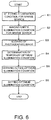
- FIG. 6 shows the flow of a processing in which the derivation of the optimum illumination condition is performed in the implementation example.
- the optimum illumination condition deriving part 124 selects, from all the illumination conditions that can be set, illumination conditions for sparse search in which the value of a prescribed element is fixed. For example, as for the illumination intensity of each LED light source, the illumination condition in which there are three gradations (for example, the illumination intensity of 0, 127, 255) and all the LED light sources are in the same illumination intensity (that is, colors of the illumination lights are white only) is selected (step S1).
- the illumination intensity of each LED light source the illumination condition in which there are three gradations (for example, the illumination intensity of 0, 127, 255) and all the LED light sources are in the same illumination intensity (that is, colors of the illumination lights are white only) is selected (step S1).
- the combinations of target illumination conditions are 81 by using 3 gradations ( 4 directions ⁇ 1color ).
- the image of the work piece W is captured under the illumination condition selected in this way (step S2), and the corresponding illumination condition is scored by the aforementioned formula (1) based on the obtained image data (step S3).
- a comparison of scores is performed on the 81 scored illumination conditions, and the illumination condition with the best score is set as the temporal optimum illumination condition (step S4).
- the steps up to this point correspond to the sparse search.
- a processing is performed in which the actual optimum illumination condition is acquired using the temporal optimum illumination condition acquired in step S4 as a reference.
- a range in which the optimum illumination condition actually exists is estimated from the temporal optimum illumination condition, and (the imaging of the work piece and) the scoring is further performed under the illumination conditions without limitation on the illumination intensity in the above range.
- the step to this point corresponds to the thorough search.
- step S5 the optimum illumination condition derived in step S5 is set as the optimum illumination condition used in the visual inspection (step S6), and the processing is completed.
- the illumination conditions that the image of the work piece is actually captured can be narrowed down even if the combination number of elements defining the illumination conditions is large, and the operator can efficiently perform the setting of the optimum illumination condition even without sufficient optical knowledge and experience.
- the setting of the optimum illumination condition is performed using a single work piece as the target, but the setting of the (leveled) optimum illumination condition using a plurality of work pieces as targets can also be performed.
- the illumination condition might be set every time for each product.
- the above problems can be solved by setting the illumination condition leveled in a prescribed deviation range (acceptable in the inspection) as the optimum illumination condition for the plurality of work pieces.
- the sparse search shown above is performed for the plurality of work pieces, and the scores at that time are saved in accordance with the plurality of work pieces. Then, the illumination condition with the smallest score in the plurality of work pieces is set as the optimum illumination condition.
- the optimum illumination condition is calculated by the following formula (2).
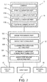
- FIG. 7 is a block diagram showing an outline of the visual inspection device 1 of this variation. As shown in FIG. 7 , compared with implementation example 1, the visual inspection device 1 of the variation is characterized in that an inspection region specifying part 125 is further provided as a function module of the control part 12.
- the inspection region specifying part 125 specifies a fixed region (also referred to as an inspection target region hereinafter) on the inspection surface of the work piece as the inspection target.
- the inspection target region is specifically determined corresponding to the work piece by an inspection specification for example and the like, and the information is registered and held in the storage part 15 in advance via the input part 14. Additionally, the information of the inspection target region may also be inputted by the operator each time.
- the specification of the region may be in any range, for example, only a specified component on the substrate may be set as the inspection target region, or only a metal portion of a fixed range may be set as the inspection target region.
- the inspection region specifying part 125 specifies, by acquiring information of the inspection target region corresponding to the work piece which is presently the inspection target, the inspection target region of the work piece. Accordingly, when the inspection target region is specified, the defect detection part 122 uses only the inspection target region as the target to perform the defect detection. Then, the optimum illumination condition deriving part 124 uses only the inspection target region as the target to perform the scoring of the image data and derive the optimum illumination condition.
- the processing (operation) necessary for scoring can be reduced and the optimum illumination condition can be set more efficiently.
- the elements determining the illumination condition are but not limited to the direction, color, illumination intensity of the illumination light; only a part of these elements may be set as the target, or other elements such as a shutter speed of the camera may be further included.
- the calculation method of the score is not limited to the above examples, for example, the illumination condition, in which a difference of the luminance values between a non-defective part and a defective part of the image obtained by imaging the work piece is the largest, may be the best score.
- One aspect of the invention is a visual inspection device 1 which includes an illumination part (112, 113, 114, 115) irradiating illumination lights to an inspection object; an imaging part 111 capturing an image of the inspection object; a defect detecting part 122 analyzing the image of the inspection object captured by the imaging part and detecting a defect of the inspection object; an illumination condition setting part 123 setting an illumination condition of the illumination light irradiated to the inspection object; and an optimum illumination condition deriving part 124 deriving an optimum illumination condition by scoring each of the illumination conditions based on images captured under a plurality of different illumination conditions, in which the optimum illumination condition is the most suitable illumination condition for detecting the defect of the inspection object by the defect detecting part.
Landscapes
- General Physics & Mathematics (AREA)
- Physics & Mathematics (AREA)
- Engineering & Computer Science (AREA)
- Immunology (AREA)
- Health & Medical Sciences (AREA)
- Biochemistry (AREA)
- General Health & Medical Sciences (AREA)
- Chemical & Material Sciences (AREA)
- Life Sciences & Earth Sciences (AREA)
- Pathology (AREA)
- Analytical Chemistry (AREA)
- Multimedia (AREA)
- Signal Processing (AREA)
- Quality & Reliability (AREA)
- Computer Vision & Pattern Recognition (AREA)
- Theoretical Computer Science (AREA)
- Investigating Materials By The Use Of Optical Means Adapted For Particular Applications (AREA)
Applications Claiming Priority (1)
| Application Number | Priority Date | Filing Date | Title |
|---|---|---|---|
| JP2018031111A JP6969439B2 (ja) | 2018-02-23 | 2018-02-23 | 外観検査装置、及び外観検査装置の照明条件設定方法 |
Publications (2)
| Publication Number | Publication Date |
|---|---|
| EP3531114A1 true EP3531114A1 (fr) | 2019-08-28 |
| EP3531114B1 EP3531114B1 (fr) | 2022-09-21 |
Family
ID=64665002
Family Applications (1)
| Application Number | Title | Priority Date | Filing Date |
|---|---|---|---|
| EP18211912.3A Active EP3531114B1 (fr) | 2018-02-23 | 2018-12-12 | Dispositif d'inspection visuelle et procédé de réglage des conditions d'éclairage d'un dispositif d'inspection visuelle |
Country Status (6)
| Country | Link |
|---|---|
| US (1) | US10805552B2 (fr) |
| EP (1) | EP3531114B1 (fr) |
| JP (1) | JP6969439B2 (fr) |
| KR (1) | KR102178903B1 (fr) |
| CN (1) | CN110186926A (fr) |
| TW (1) | TWI676796B (fr) |
Cited By (2)
| Publication number | Priority date | Publication date | Assignee | Title |
|---|---|---|---|---|
| IT201900015476A1 (it) * | 2019-09-03 | 2021-03-03 | Genesi Elettr S R L | Sistema di controllo qualità in linea e procedimento per effettuare un controllo qualità in linea |
| WO2024175875A1 (fr) * | 2023-02-20 | 2024-08-29 | University Of Strathclyde | Système et procédé de capture d'anomalie |
Families Citing this family (24)
| Publication number | Priority date | Publication date | Assignee | Title |
|---|---|---|---|---|
| JP6969439B2 (ja) * | 2018-02-23 | 2021-11-24 | オムロン株式会社 | 外観検査装置、及び外観検査装置の照明条件設定方法 |
| US10762622B2 (en) * | 2018-09-19 | 2020-09-01 | Kyocera Document Solutions Inc. | Fabric inspection device and ink-jet printing device therewith |
| WO2020175576A1 (fr) * | 2019-02-27 | 2020-09-03 | 京セラ株式会社 | Système d'éclairage, dispositif d'éclairage et procédé de commande d'éclairage |
| IT201900005536A1 (it) * | 2019-04-10 | 2020-10-10 | Doss Visual Solution S R L | Metodo di acquisizione immagini per una macchina di ispezione ottica |
| WO2020221840A1 (fr) * | 2019-04-30 | 2020-11-05 | Signify Holding B.V. | Commande d'éclairage basé sur caméra |
| CN110596124A (zh) * | 2019-10-18 | 2019-12-20 | 杭州云华视觉科技有限公司 | 一种用于瑕疵检测的图像获取装置以及瑕疵检测系统 |
| JP6860098B1 (ja) * | 2020-02-10 | 2021-04-14 | オムロン株式会社 | 画像検査装置および画像検査プログラム、照明設定装置 |
| JP7452188B2 (ja) | 2020-03-30 | 2024-03-19 | オムロン株式会社 | 検査装置 |
| CN112040138B (zh) * | 2020-08-31 | 2021-12-14 | 英华达(上海)科技有限公司 | 立体光源系统、摄像方法、装置、存储介质及电子设备 |
| JP7604190B2 (ja) * | 2020-11-25 | 2024-12-23 | キヤノン株式会社 | 検査システム、管理装置、検査方法、プログラム、記録媒体および物品の製造方法 |
| CN113194222B (zh) * | 2021-03-18 | 2023-06-27 | 优尼特克斯公司 | 一种组合成像装置 |
| WO2022214853A1 (fr) | 2021-04-08 | 2022-10-13 | University Of Moratuwa | Procédé et appareil de détection de défauts de surface |
| CN113155845A (zh) * | 2021-04-09 | 2021-07-23 | 武汉精测电子集团股份有限公司 | 一种光源及其设置方法、光学检测方法及系统 |
| JP7613996B2 (ja) * | 2021-04-16 | 2025-01-15 | 株式会社キーエンス | 画像検査装置、画像検査装置用制御ユニット、画像検査方法、画像検査プログラム及びコンピュータで読取可能な記録媒体並びに記録した機器 |
| US20230030276A1 (en) * | 2021-07-31 | 2023-02-02 | Cognex Corporation | Machine vision system and method with multispectral light assembly |
| CN113670935A (zh) * | 2021-08-25 | 2021-11-19 | 武汉中导光电设备有限公司 | 一种半导体晶圆缺陷检测设备及检测方法 |
| DE112021008348T5 (de) * | 2021-12-17 | 2024-08-08 | Fanuc Corporation | Einlernvorrichtung |
| KR102933540B1 (ko) * | 2022-03-30 | 2026-03-04 | 현대제철 주식회사 | 금속분리판의 외관 검사 장치 및 방법 |
| EP4407302A4 (fr) * | 2022-12-14 | 2025-03-05 | Contemporary Amperex Technology (Hong Kong) Limited | Appareil de détection optique, procédé et appareil de détection, dispositif électronique et support de stockage |
| CN119603832B (zh) * | 2023-09-11 | 2025-11-07 | 中国石油化工股份有限公司 | 一种用于表面缺陷检测的光源强度调节方法及系统 |
| JP7501771B1 (ja) * | 2023-12-13 | 2024-06-18 | 株式会社サタケ | 光学式判別装置及び光学式選別装置 |
| CN117849051A (zh) * | 2023-12-27 | 2024-04-09 | 上海御微半导体技术有限公司 | 缺陷检测系统、方法、装置、设备及存储介质 |
| TWI898376B (zh) * | 2023-12-29 | 2025-09-21 | 台亞半導體股份有限公司 | 半導體元件檢測裝置及其檢測方法 |
| US20250237493A1 (en) * | 2024-01-24 | 2025-07-24 | MIDGEA, GmbH | Stringed Instrument Scanning System and Related Methods |
Citations (3)
| Publication number | Priority date | Publication date | Assignee | Title |
|---|---|---|---|---|
| US20050007593A1 (en) * | 1999-07-08 | 2005-01-13 | Ppt Vision, Inc. | Method and apparatus for adjusting illumination angle |
| EP1710566A2 (fr) * | 2005-04-08 | 2006-10-11 | Omron Corporation | Méthode d'inspection d'un défaut et système d'inspection d'un défaut utilisant la méthode |
| JP2018017638A (ja) | 2016-07-29 | 2018-02-01 | オムロン株式会社 | 照明ユニット、欠陥検査装置、および照明方法 |
Family Cites Families (24)
| Publication number | Priority date | Publication date | Assignee | Title |
|---|---|---|---|---|
| JPH11281334A (ja) * | 1998-03-27 | 1999-10-15 | Vanguard Systems:Kk | 部品検査装置 |
| JP2003121380A (ja) * | 2001-10-11 | 2003-04-23 | Nikon Corp | 表面検査装置および表面検査方法 |
| JP3551188B2 (ja) * | 2002-01-10 | 2004-08-04 | オムロン株式会社 | 表面状態検査方法および基板検査装置 |
| JP2003270163A (ja) * | 2002-03-15 | 2003-09-25 | Dainippon Printing Co Ltd | 検査方法および装置 |
| JP3867724B2 (ja) * | 2004-02-27 | 2007-01-10 | オムロン株式会社 | 表面状態検査方法およびその方法を用いた表面状態検査装置ならびに基板検査装置 |
| US7366321B2 (en) * | 2004-06-18 | 2008-04-29 | Agilent Technologies, Inc. | System and method for performing automated optical inspection of objects |
| EP1612569A3 (fr) | 2004-06-30 | 2006-02-08 | Omron Corporation | Procédé et appareil permettant d'inspecter la surface d'un substrat avec un système d'émission de lumière multicolore |
| US7769226B2 (en) * | 2005-01-26 | 2010-08-03 | Semiconductor Energy Laboratory Co., Ltd. | Pattern inspection method and apparatus |
| JP4935109B2 (ja) * | 2005-03-17 | 2012-05-23 | オムロン株式会社 | 基板検査装置並びにその検査ロジック設定方法および検査ロジック設定装置 |
| CN1844901A (zh) * | 2005-04-08 | 2006-10-11 | 欧姆龙株式会社 | 缺陷检查方法以及利用该方法的缺陷检查装置 |
| JP4079977B2 (ja) * | 2006-09-19 | 2008-04-23 | シーシーエス株式会社 | 画像処理用光照射装置及び画像処理用光照射方法 |
| WO2008124397A1 (fr) * | 2007-04-03 | 2008-10-16 | David Fishbaine | Système et procédé d'inspection |
| KR101193728B1 (ko) * | 2007-12-05 | 2012-10-22 | 시바우라 메카트로닉스 가부시키가이샤 | 특징 해석 장치 |
| EP2394295A2 (fr) * | 2009-02-06 | 2011-12-14 | KLA-Tencor Corporation | Sélection d'un ou plusieurs paramètres pour l'inspection d'une tranche |
| JPWO2012090416A1 (ja) * | 2010-12-28 | 2014-06-05 | オリンパス株式会社 | 検査装置 |
| CN103163741B (zh) | 2011-12-14 | 2014-12-17 | 上海微电子装备有限公司 | 光刻机可变狭缝最佳位置的测量方法 |
| JP2014044150A (ja) | 2012-08-28 | 2014-03-13 | Toppan Printing Co Ltd | 周期性パターンの欠陥検査方法 |
| US10274835B2 (en) * | 2012-12-20 | 2019-04-30 | Nikon Corporation | Evaluation method and device, processing method, and exposure system |
| JP7026309B2 (ja) * | 2015-01-29 | 2022-02-28 | 株式会社 デクシス | 光学式外観検査装置、及びこれを用いた光学式外観検査システム |
| JP6601264B2 (ja) | 2016-02-29 | 2019-11-06 | 富士通株式会社 | 照明条件設定装置、照明条件設定方法及び照明条件設定用コンピュータプログラム |
| JP6684158B2 (ja) * | 2016-06-13 | 2020-04-22 | 株式会社キーエンス | 画像処理センサ、画像処理方法 |
| JP6764701B2 (ja) * | 2016-06-13 | 2020-10-07 | 株式会社キーエンス | 画像処理センサ、画像処理方法、画像処理プログラム及びコンピュータで読み取り可能な記録媒体並びに記録した機器 |
| JP6730855B2 (ja) * | 2016-06-13 | 2020-07-29 | 株式会社キーエンス | 画像処理センサ、画像処理方法、画像処理プログラム及びコンピュータで読み取り可能な記録媒体並びに記録した機器 |
| JP6969439B2 (ja) * | 2018-02-23 | 2021-11-24 | オムロン株式会社 | 外観検査装置、及び外観検査装置の照明条件設定方法 |
-
2018
- 2018-02-23 JP JP2018031111A patent/JP6969439B2/ja active Active
- 2018-12-11 KR KR1020180158806A patent/KR102178903B1/ko active Active
- 2018-12-11 CN CN201811509322.3A patent/CN110186926A/zh active Pending
- 2018-12-12 EP EP18211912.3A patent/EP3531114B1/fr active Active
- 2018-12-14 US US16/219,950 patent/US10805552B2/en active Active
- 2018-12-17 TW TW107145495A patent/TWI676796B/zh active
Patent Citations (3)
| Publication number | Priority date | Publication date | Assignee | Title |
|---|---|---|---|---|
| US20050007593A1 (en) * | 1999-07-08 | 2005-01-13 | Ppt Vision, Inc. | Method and apparatus for adjusting illumination angle |
| EP1710566A2 (fr) * | 2005-04-08 | 2006-10-11 | Omron Corporation | Méthode d'inspection d'un défaut et système d'inspection d'un défaut utilisant la méthode |
| JP2018017638A (ja) | 2016-07-29 | 2018-02-01 | オムロン株式会社 | 照明ユニット、欠陥検査装置、および照明方法 |
Cited By (2)
| Publication number | Priority date | Publication date | Assignee | Title |
|---|---|---|---|---|
| IT201900015476A1 (it) * | 2019-09-03 | 2021-03-03 | Genesi Elettr S R L | Sistema di controllo qualità in linea e procedimento per effettuare un controllo qualità in linea |
| WO2024175875A1 (fr) * | 2023-02-20 | 2024-08-29 | University Of Strathclyde | Système et procédé de capture d'anomalie |
Also Published As
| Publication number | Publication date |
|---|---|
| KR102178903B1 (ko) | 2020-11-13 |
| US10805552B2 (en) | 2020-10-13 |
| CN110186926A (zh) | 2019-08-30 |
| KR20190101857A (ko) | 2019-09-02 |
| JP6969439B2 (ja) | 2021-11-24 |
| TWI676796B (zh) | 2019-11-11 |
| JP2019144209A (ja) | 2019-08-29 |
| TW201937157A (zh) | 2019-09-16 |
| US20190268522A1 (en) | 2019-08-29 |
| EP3531114B1 (fr) | 2022-09-21 |
Similar Documents
| Publication | Publication Date | Title |
|---|---|---|
| EP3531114B1 (fr) | Dispositif d'inspection visuelle et procédé de réglage des conditions d'éclairage d'un dispositif d'inspection visuelle | |
| EP2148189B1 (fr) | Procédé, dispositif et programme de contrôle du bois d' oeuvre | |
| US20200018707A1 (en) | Appearance inspection device, lighting device, and imaging lighting device | |
| JP5424659B2 (ja) | 被検査体の検査装置 | |
| CN108445007A (zh) | 一种基于图像融合的检测方法及其检测装置 | |
| US20170053394A1 (en) | Inspection apparatus, inspection method, and article manufacturing method | |
| US20240354930A1 (en) | System and method for defect detection using visible light cameras with synchronized lighting | |
| JP5589888B2 (ja) | 表面検査装置の評価装置及び表面検査装置の評価方法 | |
| CN108663371B (zh) | 一种检测显示面板灰尘异物的方法及系统 | |
| KR20140091916A (ko) | 디스플레이 패널 검사방법 | |
| KR101679314B1 (ko) | 다중 노광을 운용한 중복 노광 화상 믹싱의 검사 방법 | |
| JP5424660B2 (ja) | 被検査体の検査装置 | |
| KR101362171B1 (ko) | 표시 장치의 검사 장치 및 방법 | |
| JP2009156872A6 (ja) | 被検査体の検査装置 | |
| JP5634390B2 (ja) | ガラス容器の欠陥検査方法及び装置 | |
| JP2010256113A (ja) | カラーフィルタの外観検査方法及び外観検査装置 | |
| KR102117697B1 (ko) | 표면검사 장치 및 방법 | |
| JP6260175B2 (ja) | サインパネル検査システム、サインパネル検査方法 | |
| KR20230114403A (ko) | 패턴 주사 조명을 이용한 투명 재질의 공산품 결함 검출 시스템 | |
| CN111665260B (zh) | 显示面板检查装置 | |
| KR20110117371A (ko) | 패턴 검사 장치 | |
| JP2010008125A (ja) | ガラス基板内の気泡選別処理法 | |
| JP4371883B2 (ja) | 検査用照明光源ユニットとこの光源ユニットを用いた表面欠陥検査装置 | |
| JP2025150370A (ja) | 外観検査システム、外観検査装置、外観検査装置の制御方法及びプログラム | |
| JP2025010546A (ja) | 画像形成システム、画像形成方法、及びプログラム |
Legal Events
| Date | Code | Title | Description |
|---|---|---|---|
| PUAI | Public reference made under article 153(3) epc to a published international application that has entered the european phase |
Free format text: ORIGINAL CODE: 0009012 |
|
| STAA | Information on the status of an ep patent application or granted ep patent |
Free format text: STATUS: REQUEST FOR EXAMINATION WAS MADE |
|
| 17P | Request for examination filed |
Effective date: 20181212 |
|
| AK | Designated contracting states |
Kind code of ref document: A1 Designated state(s): AL AT BE BG CH CY CZ DE DK EE ES FI FR GB GR HR HU IE IS IT LI LT LU LV MC MK MT NL NO PL PT RO RS SE SI SK SM TR |
|
| AX | Request for extension of the european patent |
Extension state: BA ME |
|
| RBV | Designated contracting states (corrected) |
Designated state(s): AL AT BE BG CH CY CZ DE DK EE ES FI FR GB GR HR HU IE IS IT LI LT LU LV MC MK MT NL NO PL PT RO RS SE SI SK SM TR |
|
| STAA | Information on the status of an ep patent application or granted ep patent |
Free format text: STATUS: EXAMINATION IS IN PROGRESS |
|
| 17Q | First examination report despatched |
Effective date: 20200422 |
|
| GRAP | Despatch of communication of intention to grant a patent |
Free format text: ORIGINAL CODE: EPIDOSNIGR1 |
|
| STAA | Information on the status of an ep patent application or granted ep patent |
Free format text: STATUS: GRANT OF PATENT IS INTENDED |
|
| RAP3 | Party data changed (applicant data changed or rights of an application transferred) |
Owner name: OMRON CORPORATION |
|
| RIN1 | Information on inventor provided before grant (corrected) |
Inventor name: HAYASHI, SHINGO |
|
| INTG | Intention to grant announced |
Effective date: 20220502 |
|
| GRAS | Grant fee paid |
Free format text: ORIGINAL CODE: EPIDOSNIGR3 |
|
| GRAA | (expected) grant |
Free format text: ORIGINAL CODE: 0009210 |
|
| STAA | Information on the status of an ep patent application or granted ep patent |
Free format text: STATUS: THE PATENT HAS BEEN GRANTED |
|
| AK | Designated contracting states |
Kind code of ref document: B1 Designated state(s): AL AT BE BG CH CY CZ DE DK EE ES FI FR GB GR HR HU IE IS IT LI LT LU LV MC MK MT NL NO PL PT RO RS SE SI SK SM TR |
|
| REG | Reference to a national code |
Ref country code: GB Ref legal event code: FG4D |
|
| REG | Reference to a national code |
Ref country code: CH Ref legal event code: EP |
|
| REG | Reference to a national code |
Ref country code: DE Ref legal event code: R096 Ref document number: 602018040848 Country of ref document: DE |
|
| REG | Reference to a national code |
Ref country code: IE Ref legal event code: FG4D |
|
| REG | Reference to a national code |
Ref country code: AT Ref legal event code: REF Ref document number: 1520170 Country of ref document: AT Kind code of ref document: T Effective date: 20221015 |
|
| REG | Reference to a national code |
Ref country code: LT Ref legal event code: MG9D |
|
| REG | Reference to a national code |
Ref country code: NL Ref legal event code: MP Effective date: 20220921 |
|
| PG25 | Lapsed in a contracting state [announced via postgrant information from national office to epo] |
Ref country code: SE Free format text: LAPSE BECAUSE OF FAILURE TO SUBMIT A TRANSLATION OF THE DESCRIPTION OR TO PAY THE FEE WITHIN THE PRESCRIBED TIME-LIMIT Effective date: 20220921 Ref country code: RS Free format text: LAPSE BECAUSE OF FAILURE TO SUBMIT A TRANSLATION OF THE DESCRIPTION OR TO PAY THE FEE WITHIN THE PRESCRIBED TIME-LIMIT Effective date: 20220921 Ref country code: NO Free format text: LAPSE BECAUSE OF FAILURE TO SUBMIT A TRANSLATION OF THE DESCRIPTION OR TO PAY THE FEE WITHIN THE PRESCRIBED TIME-LIMIT Effective date: 20221221 Ref country code: LV Free format text: LAPSE BECAUSE OF FAILURE TO SUBMIT A TRANSLATION OF THE DESCRIPTION OR TO PAY THE FEE WITHIN THE PRESCRIBED TIME-LIMIT Effective date: 20220921 Ref country code: LT Free format text: LAPSE BECAUSE OF FAILURE TO SUBMIT A TRANSLATION OF THE DESCRIPTION OR TO PAY THE FEE WITHIN THE PRESCRIBED TIME-LIMIT Effective date: 20220921 Ref country code: FI Free format text: LAPSE BECAUSE OF FAILURE TO SUBMIT A TRANSLATION OF THE DESCRIPTION OR TO PAY THE FEE WITHIN THE PRESCRIBED TIME-LIMIT Effective date: 20220921 |
|
| REG | Reference to a national code |
Ref country code: AT Ref legal event code: MK05 Ref document number: 1520170 Country of ref document: AT Kind code of ref document: T Effective date: 20220921 |
|
| PG25 | Lapsed in a contracting state [announced via postgrant information from national office to epo] |
Ref country code: HR Free format text: LAPSE BECAUSE OF FAILURE TO SUBMIT A TRANSLATION OF THE DESCRIPTION OR TO PAY THE FEE WITHIN THE PRESCRIBED TIME-LIMIT Effective date: 20220921 Ref country code: GR Free format text: LAPSE BECAUSE OF FAILURE TO SUBMIT A TRANSLATION OF THE DESCRIPTION OR TO PAY THE FEE WITHIN THE PRESCRIBED TIME-LIMIT Effective date: 20221222 |
|
| PG25 | Lapsed in a contracting state [announced via postgrant information from national office to epo] |
Ref country code: SM Free format text: LAPSE BECAUSE OF FAILURE TO SUBMIT A TRANSLATION OF THE DESCRIPTION OR TO PAY THE FEE WITHIN THE PRESCRIBED TIME-LIMIT Effective date: 20220921 Ref country code: RO Free format text: LAPSE BECAUSE OF FAILURE TO SUBMIT A TRANSLATION OF THE DESCRIPTION OR TO PAY THE FEE WITHIN THE PRESCRIBED TIME-LIMIT Effective date: 20220921 Ref country code: PT Free format text: LAPSE BECAUSE OF FAILURE TO SUBMIT A TRANSLATION OF THE DESCRIPTION OR TO PAY THE FEE WITHIN THE PRESCRIBED TIME-LIMIT Effective date: 20230123 Ref country code: ES Free format text: LAPSE BECAUSE OF FAILURE TO SUBMIT A TRANSLATION OF THE DESCRIPTION OR TO PAY THE FEE WITHIN THE PRESCRIBED TIME-LIMIT Effective date: 20220921 Ref country code: CZ Free format text: LAPSE BECAUSE OF FAILURE TO SUBMIT A TRANSLATION OF THE DESCRIPTION OR TO PAY THE FEE WITHIN THE PRESCRIBED TIME-LIMIT Effective date: 20220921 Ref country code: AT Free format text: LAPSE BECAUSE OF FAILURE TO SUBMIT A TRANSLATION OF THE DESCRIPTION OR TO PAY THE FEE WITHIN THE PRESCRIBED TIME-LIMIT Effective date: 20220921 |
|
| PG25 | Lapsed in a contracting state [announced via postgrant information from national office to epo] |
Ref country code: SK Free format text: LAPSE BECAUSE OF FAILURE TO SUBMIT A TRANSLATION OF THE DESCRIPTION OR TO PAY THE FEE WITHIN THE PRESCRIBED TIME-LIMIT Effective date: 20220921 Ref country code: PL Free format text: LAPSE BECAUSE OF FAILURE TO SUBMIT A TRANSLATION OF THE DESCRIPTION OR TO PAY THE FEE WITHIN THE PRESCRIBED TIME-LIMIT Effective date: 20220921 Ref country code: IS Free format text: LAPSE BECAUSE OF FAILURE TO SUBMIT A TRANSLATION OF THE DESCRIPTION OR TO PAY THE FEE WITHIN THE PRESCRIBED TIME-LIMIT Effective date: 20230121 Ref country code: EE Free format text: LAPSE BECAUSE OF FAILURE TO SUBMIT A TRANSLATION OF THE DESCRIPTION OR TO PAY THE FEE WITHIN THE PRESCRIBED TIME-LIMIT Effective date: 20220921 |
|
| REG | Reference to a national code |
Ref country code: DE Ref legal event code: R097 Ref document number: 602018040848 Country of ref document: DE |
|
| PG25 | Lapsed in a contracting state [announced via postgrant information from national office to epo] |
Ref country code: NL Free format text: LAPSE BECAUSE OF FAILURE TO SUBMIT A TRANSLATION OF THE DESCRIPTION OR TO PAY THE FEE WITHIN THE PRESCRIBED TIME-LIMIT Effective date: 20220921 Ref country code: AL Free format text: LAPSE BECAUSE OF FAILURE TO SUBMIT A TRANSLATION OF THE DESCRIPTION OR TO PAY THE FEE WITHIN THE PRESCRIBED TIME-LIMIT Effective date: 20220921 |
|
| PLBE | No opposition filed within time limit |
Free format text: ORIGINAL CODE: 0009261 |
|
| STAA | Information on the status of an ep patent application or granted ep patent |
Free format text: STATUS: NO OPPOSITION FILED WITHIN TIME LIMIT |
|
| PG25 | Lapsed in a contracting state [announced via postgrant information from national office to epo] |
Ref country code: DK Free format text: LAPSE BECAUSE OF FAILURE TO SUBMIT A TRANSLATION OF THE DESCRIPTION OR TO PAY THE FEE WITHIN THE PRESCRIBED TIME-LIMIT Effective date: 20220921 |
|
| REG | Reference to a national code |
Ref country code: CH Ref legal event code: PL |
|
| GBPC | Gb: european patent ceased through non-payment of renewal fee |
Effective date: 20221221 |
|
| REG | Reference to a national code |
Ref country code: BE Ref legal event code: MM Effective date: 20221231 |
|
| 26N | No opposition filed |
Effective date: 20230622 |
|
| PG25 | Lapsed in a contracting state [announced via postgrant information from national office to epo] |
Ref country code: SI Free format text: LAPSE BECAUSE OF FAILURE TO SUBMIT A TRANSLATION OF THE DESCRIPTION OR TO PAY THE FEE WITHIN THE PRESCRIBED TIME-LIMIT Effective date: 20220921 Ref country code: LU Free format text: LAPSE BECAUSE OF NON-PAYMENT OF DUE FEES Effective date: 20221212 |
|
| PG25 | Lapsed in a contracting state [announced via postgrant information from national office to epo] |
Ref country code: LI Free format text: LAPSE BECAUSE OF NON-PAYMENT OF DUE FEES Effective date: 20221231 Ref country code: IE Free format text: LAPSE BECAUSE OF NON-PAYMENT OF DUE FEES Effective date: 20221212 Ref country code: GB Free format text: LAPSE BECAUSE OF NON-PAYMENT OF DUE FEES Effective date: 20221221 Ref country code: CH Free format text: LAPSE BECAUSE OF NON-PAYMENT OF DUE FEES Effective date: 20221231 |
|
| PG25 | Lapsed in a contracting state [announced via postgrant information from national office to epo] |
Ref country code: FR Free format text: LAPSE BECAUSE OF NON-PAYMENT OF DUE FEES Effective date: 20221231 Ref country code: BE Free format text: LAPSE BECAUSE OF NON-PAYMENT OF DUE FEES Effective date: 20221231 |
|
| PG25 | Lapsed in a contracting state [announced via postgrant information from national office to epo] |
Ref country code: HU Free format text: LAPSE BECAUSE OF FAILURE TO SUBMIT A TRANSLATION OF THE DESCRIPTION OR TO PAY THE FEE WITHIN THE PRESCRIBED TIME-LIMIT; INVALID AB INITIO Effective date: 20181212 |
|
| PG25 | Lapsed in a contracting state [announced via postgrant information from national office to epo] |
Ref country code: CY Free format text: LAPSE BECAUSE OF FAILURE TO SUBMIT A TRANSLATION OF THE DESCRIPTION OR TO PAY THE FEE WITHIN THE PRESCRIBED TIME-LIMIT Effective date: 20220921 |
|
| PG25 | Lapsed in a contracting state [announced via postgrant information from national office to epo] |
Ref country code: MK Free format text: LAPSE BECAUSE OF FAILURE TO SUBMIT A TRANSLATION OF THE DESCRIPTION OR TO PAY THE FEE WITHIN THE PRESCRIBED TIME-LIMIT Effective date: 20220921 Ref country code: IT Free format text: LAPSE BECAUSE OF FAILURE TO SUBMIT A TRANSLATION OF THE DESCRIPTION OR TO PAY THE FEE WITHIN THE PRESCRIBED TIME-LIMIT Effective date: 20220921 |
|
| PG25 | Lapsed in a contracting state [announced via postgrant information from national office to epo] |
Ref country code: MC Free format text: LAPSE BECAUSE OF FAILURE TO SUBMIT A TRANSLATION OF THE DESCRIPTION OR TO PAY THE FEE WITHIN THE PRESCRIBED TIME-LIMIT Effective date: 20220921 |
|
| PG25 | Lapsed in a contracting state [announced via postgrant information from national office to epo] |
Ref country code: TR Free format text: LAPSE BECAUSE OF FAILURE TO SUBMIT A TRANSLATION OF THE DESCRIPTION OR TO PAY THE FEE WITHIN THE PRESCRIBED TIME-LIMIT Effective date: 20220921 Ref country code: MC Free format text: LAPSE BECAUSE OF FAILURE TO SUBMIT A TRANSLATION OF THE DESCRIPTION OR TO PAY THE FEE WITHIN THE PRESCRIBED TIME-LIMIT Effective date: 20220921 |
|
| PG25 | Lapsed in a contracting state [announced via postgrant information from national office to epo] |
Ref country code: BG Free format text: LAPSE BECAUSE OF FAILURE TO SUBMIT A TRANSLATION OF THE DESCRIPTION OR TO PAY THE FEE WITHIN THE PRESCRIBED TIME-LIMIT Effective date: 20220921 |
|
| PG25 | Lapsed in a contracting state [announced via postgrant information from national office to epo] |
Ref country code: MT Free format text: LAPSE BECAUSE OF FAILURE TO SUBMIT A TRANSLATION OF THE DESCRIPTION OR TO PAY THE FEE WITHIN THE PRESCRIBED TIME-LIMIT Effective date: 20220921 |
|
| PGFP | Annual fee paid to national office [announced via postgrant information from national office to epo] |
Ref country code: DE Payment date: 20251222 Year of fee payment: 8 |