EP3531265A1 - Procédé de mémoire cache basé sur une dram, et terminal intelligent - Google Patents
Procédé de mémoire cache basé sur une dram, et terminal intelligent Download PDFInfo
- Publication number
- EP3531265A1 EP3531265A1 EP17866977.6A EP17866977A EP3531265A1 EP 3531265 A1 EP3531265 A1 EP 3531265A1 EP 17866977 A EP17866977 A EP 17866977A EP 3531265 A1 EP3531265 A1 EP 3531265A1
- Authority
- EP
- European Patent Office
- Prior art keywords
- dram
- type
- caching
- data
- write
- Prior art date
- Legal status (The legal status is an assumption and is not a legal conclusion. Google has not performed a legal analysis and makes no representation as to the accuracy of the status listed.)
- Ceased
Links
Images



Classifications
-
- G—PHYSICS
- G06—COMPUTING OR CALCULATING; COUNTING
- G06F—ELECTRIC DIGITAL DATA PROCESSING
- G06F12/00—Accessing, addressing or allocating within memory systems or architectures
- G06F12/02—Addressing or allocation; Relocation
- G06F12/08—Addressing or allocation; Relocation in hierarchically structured memory systems, e.g. virtual memory systems
- G06F12/0802—Addressing of a memory level in which the access to the desired data or data block requires associative addressing means, e.g. caches
- G06F12/0893—Caches characterised by their organisation or structure
-
- G—PHYSICS
- G06—COMPUTING OR CALCULATING; COUNTING
- G06F—ELECTRIC DIGITAL DATA PROCESSING
- G06F3/00—Input arrangements for transferring data to be processed into a form capable of being handled by the computer; Output arrangements for transferring data from processing unit to output unit, e.g. interface arrangements
- G06F3/06—Digital input from, or digital output to, record carriers, e.g. RAID, emulated record carriers or networked record carriers
- G06F3/0601—Interfaces specially adapted for storage systems
- G06F3/0668—Interfaces specially adapted for storage systems adopting a particular infrastructure
- G06F3/0671—In-line storage system
- G06F3/0683—Plurality of storage devices
- G06F3/0685—Hybrid storage combining heterogeneous device types, e.g. hierarchical storage, hybrid arrays
-
- G—PHYSICS
- G06—COMPUTING OR CALCULATING; COUNTING
- G06F—ELECTRIC DIGITAL DATA PROCESSING
- G06F12/00—Accessing, addressing or allocating within memory systems or architectures
- G06F12/02—Addressing or allocation; Relocation
- G06F12/08—Addressing or allocation; Relocation in hierarchically structured memory systems, e.g. virtual memory systems
- G06F12/0802—Addressing of a memory level in which the access to the desired data or data block requires associative addressing means, e.g. caches
- G06F12/0804—Addressing of a memory level in which the access to the desired data or data block requires associative addressing means, e.g. caches with main memory updating
-
- G—PHYSICS
- G06—COMPUTING OR CALCULATING; COUNTING
- G06F—ELECTRIC DIGITAL DATA PROCESSING
- G06F12/00—Accessing, addressing or allocating within memory systems or architectures
- G06F12/02—Addressing or allocation; Relocation
- G06F12/08—Addressing or allocation; Relocation in hierarchically structured memory systems, e.g. virtual memory systems
- G06F12/0802—Addressing of a memory level in which the access to the desired data or data block requires associative addressing means, e.g. caches
- G06F12/0866—Addressing of a memory level in which the access to the desired data or data block requires associative addressing means, e.g. caches for peripheral storage systems, e.g. disk cache
- G06F12/0868—Data transfer between cache memory and other subsystems, e.g. storage devices or host systems
-
- G—PHYSICS
- G06—COMPUTING OR CALCULATING; COUNTING
- G06F—ELECTRIC DIGITAL DATA PROCESSING
- G06F12/00—Accessing, addressing or allocating within memory systems or architectures
- G06F12/02—Addressing or allocation; Relocation
- G06F12/08—Addressing or allocation; Relocation in hierarchically structured memory systems, e.g. virtual memory systems
- G06F12/0802—Addressing of a memory level in which the access to the desired data or data block requires associative addressing means, e.g. caches
- G06F12/0866—Addressing of a memory level in which the access to the desired data or data block requires associative addressing means, e.g. caches for peripheral storage systems, e.g. disk cache
- G06F12/0871—Allocation or management of cache space
-
- G—PHYSICS
- G06—COMPUTING OR CALCULATING; COUNTING
- G06F—ELECTRIC DIGITAL DATA PROCESSING
- G06F12/00—Accessing, addressing or allocating within memory systems or architectures
- G06F12/02—Addressing or allocation; Relocation
- G06F12/08—Addressing or allocation; Relocation in hierarchically structured memory systems, e.g. virtual memory systems
- G06F12/0802—Addressing of a memory level in which the access to the desired data or data block requires associative addressing means, e.g. caches
- G06F12/0888—Addressing of a memory level in which the access to the desired data or data block requires associative addressing means, e.g. caches using selective caching, e.g. bypass
-
- G—PHYSICS
- G06—COMPUTING OR CALCULATING; COUNTING
- G06F—ELECTRIC DIGITAL DATA PROCESSING
- G06F3/00—Input arrangements for transferring data to be processed into a form capable of being handled by the computer; Output arrangements for transferring data from processing unit to output unit, e.g. interface arrangements
- G06F3/06—Digital input from, or digital output to, record carriers, e.g. RAID, emulated record carriers or networked record carriers
-
- G—PHYSICS
- G06—COMPUTING OR CALCULATING; COUNTING
- G06F—ELECTRIC DIGITAL DATA PROCESSING
- G06F3/00—Input arrangements for transferring data to be processed into a form capable of being handled by the computer; Output arrangements for transferring data from processing unit to output unit, e.g. interface arrangements
- G06F3/06—Digital input from, or digital output to, record carriers, e.g. RAID, emulated record carriers or networked record carriers
- G06F3/0601—Interfaces specially adapted for storage systems
- G06F3/0602—Interfaces specially adapted for storage systems specifically adapted to achieve a particular effect
- G06F3/061—Improving I/O performance
-
- G—PHYSICS
- G06—COMPUTING OR CALCULATING; COUNTING
- G06F—ELECTRIC DIGITAL DATA PROCESSING
- G06F3/00—Input arrangements for transferring data to be processed into a form capable of being handled by the computer; Output arrangements for transferring data from processing unit to output unit, e.g. interface arrangements
- G06F3/06—Digital input from, or digital output to, record carriers, e.g. RAID, emulated record carriers or networked record carriers
- G06F3/0601—Interfaces specially adapted for storage systems
- G06F3/0628—Interfaces specially adapted for storage systems making use of a particular technique
- G06F3/0646—Horizontal data movement in storage systems, i.e. moving data in between storage devices or systems
-
- G—PHYSICS
- G06—COMPUTING OR CALCULATING; COUNTING
- G06F—ELECTRIC DIGITAL DATA PROCESSING
- G06F3/00—Input arrangements for transferring data to be processed into a form capable of being handled by the computer; Output arrangements for transferring data from processing unit to output unit, e.g. interface arrangements
- G06F3/06—Digital input from, or digital output to, record carriers, e.g. RAID, emulated record carriers or networked record carriers
- G06F3/0601—Interfaces specially adapted for storage systems
- G06F3/0628—Interfaces specially adapted for storage systems making use of a particular technique
- G06F3/0655—Vertical data movement, i.e. input-output transfer; data movement between one or more hosts and one or more storage devices
-
- G—PHYSICS
- G06—COMPUTING OR CALCULATING; COUNTING
- G06F—ELECTRIC DIGITAL DATA PROCESSING
- G06F3/00—Input arrangements for transferring data to be processed into a form capable of being handled by the computer; Output arrangements for transferring data from processing unit to output unit, e.g. interface arrangements
- G06F3/06—Digital input from, or digital output to, record carriers, e.g. RAID, emulated record carriers or networked record carriers
- G06F3/0601—Interfaces specially adapted for storage systems
- G06F3/0628—Interfaces specially adapted for storage systems making use of a particular technique
- G06F3/0655—Vertical data movement, i.e. input-output transfer; data movement between one or more hosts and one or more storage devices
- G06F3/0656—Data buffering arrangements
-
- G—PHYSICS
- G06—COMPUTING OR CALCULATING; COUNTING
- G06F—ELECTRIC DIGITAL DATA PROCESSING
- G06F3/00—Input arrangements for transferring data to be processed into a form capable of being handled by the computer; Output arrangements for transferring data from processing unit to output unit, e.g. interface arrangements
- G06F3/06—Digital input from, or digital output to, record carriers, e.g. RAID, emulated record carriers or networked record carriers
- G06F3/0601—Interfaces specially adapted for storage systems
- G06F3/0668—Interfaces specially adapted for storage systems adopting a particular infrastructure
- G06F3/0671—In-line storage system
- G06F3/0673—Single storage device
- G06F3/0679—Non-volatile semiconductor memory device, e.g. flash memory, one time programmable memory [OTP]
-
- G—PHYSICS
- G06—COMPUTING OR CALCULATING; COUNTING
- G06F—ELECTRIC DIGITAL DATA PROCESSING
- G06F3/00—Input arrangements for transferring data to be processed into a form capable of being handled by the computer; Output arrangements for transferring data from processing unit to output unit, e.g. interface arrangements
- G06F3/06—Digital input from, or digital output to, record carriers, e.g. RAID, emulated record carriers or networked record carriers
- G06F3/0601—Interfaces specially adapted for storage systems
- G06F3/0668—Interfaces specially adapted for storage systems adopting a particular infrastructure
- G06F3/0671—In-line storage system
- G06F3/0683—Plurality of storage devices
- G06F3/0688—Non-volatile semiconductor memory arrays
-
- G—PHYSICS
- G06—COMPUTING OR CALCULATING; COUNTING
- G06F—ELECTRIC DIGITAL DATA PROCESSING
- G06F2212/00—Indexing scheme relating to accessing, addressing or allocation within memory systems or architectures
- G06F2212/10—Providing a specific technical effect
- G06F2212/1016—Performance improvement
-
- G—PHYSICS
- G06—COMPUTING OR CALCULATING; COUNTING
- G06F—ELECTRIC DIGITAL DATA PROCESSING
- G06F2212/00—Indexing scheme relating to accessing, addressing or allocation within memory systems or architectures
- G06F2212/22—Employing cache memory using specific memory technology
- G06F2212/224—Disk storage
-
- G—PHYSICS
- G06—COMPUTING OR CALCULATING; COUNTING
- G06F—ELECTRIC DIGITAL DATA PROCESSING
- G06F2212/00—Indexing scheme relating to accessing, addressing or allocation within memory systems or architectures
- G06F2212/30—Providing cache or TLB in specific location of a processing system
- G06F2212/305—Providing cache or TLB in specific location of a processing system being part of a memory device, e.g. cache DRAM
-
- G—PHYSICS
- G06—COMPUTING OR CALCULATING; COUNTING
- G06F—ELECTRIC DIGITAL DATA PROCESSING
- G06F2212/00—Indexing scheme relating to accessing, addressing or allocation within memory systems or architectures
- G06F2212/31—Providing disk cache in a specific location of a storage system
- G06F2212/313—In storage device
-
- G—PHYSICS
- G06—COMPUTING OR CALCULATING; COUNTING
- G06F—ELECTRIC DIGITAL DATA PROCESSING
- G06F2212/00—Indexing scheme relating to accessing, addressing or allocation within memory systems or architectures
- G06F2212/46—Caching storage objects of specific type in disk cache
- G06F2212/461—Sector or disk block
Definitions
- the present invention relates to the storage field, and in particular, to a DRAM-based storage caching method and a DRAM-based smart terminal.
- eMMC Solid State Drives, solid state drive
- SSD Solid State Drives, solid state drive
- Advantages of this flash medium over a conventional storage medium are better random read/write performance, lower power consumption, and higher storage density.
- flash storage media also have distinct disadvantages. For example, performance of random small-sized IOs is still far below performance of large-sized sequential IOs, and a quantity of writes on the storage medium is limited, while the quantity of writes directly affects a service life of the storage device.
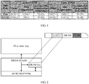
- FIG. 1 shows test data of IO write and IO rewrite performance before and after fragmentation of storage space. It can be seen that IO performance after fragmentation declines drastically. This is because, after the storage device is seriously fragmented, an IO write is split into a plurality of IOs due to fragmentation of the space. As a result, a quantity of IOs delivered to a bottom-layer block device is increased, and a size of each IO is reduced.
- a small-sized IO entails more additional non-IO data overheads (for example, a quantity of IO commands) on a full path of IO transmission, and this leads to drastic decline of the IO performance.
- Embodiments of the present invention provide a DRAM-based storage caching method and a DRAM-based smart terminal, to improve IO performance.
- One aspect of the present invention provides a DRAM-based storage caching method, applied to a smart terminal, where the method includes:
- the determining, according to based on a configuration policy, whether the IO belongs to a prespecified to-be-cached IO type includes:
- the determining, according to based on a configuration policy, whether the IO belongs to a prespecified to-be-cached IO type specifically includes:
- the DRAM disk is a block device created by using a reserved DRAM.
- this DRAM region is masked by using bottom-layer firmware, so that the DRAM is invisible to an OS, avoiding that the DRAM is allocated to another module by the operating system for use.
- this DRAM region may be set to be reserved when bottom-layer firmware reports system global memory information to the OS, to avoid allocation to another module.
- this reserved DRAM section may be continuous space. In another embodiment, alternatively, this reserved DRAM section may be discontinuous space.
- the performing a corresponding caching operation for the IO in a DRAM disk based on a read/write type of the IO and a preset caching policy includes:
- the method further includes: when the DRAM disk is short of space, selecting to flush dirty data back into a bottom-layer device according to a preset policy.
- the method further includes: in a case of a normal switch-off of the smart terminal, before the switch-off, flushing all dirty data cached in the DRAM disk back into the bottom-layer device, and disabling caching or setting the caching policy to write-through.
- the method further includes: in a case of a forced switch-off or a restart of the smart terminal, at the beginning of the forced switch-off or the restart, flushing back the dirty data, and disabling caching or setting the caching policy to write-through.
- Another aspect of the embodiments of the present invention provides a terminal provided with a DRAM, where the terminal includes:
- the judgment module includes:
- the judgment module includes:
- the caching operation module includes:
- the embodiments of the present invention provide a storage caching technology that is based on a DRAM dynamic random access memory, so that performance of random small-sized IOs on a terminal device is improved on a basis of an existing DRAM memory and a block storage device. Also, with the technology of the embodiments of the present invention, a problem of fragmentation of storage space caused by large quantities of random IOs and rewrite operations can be alleviated. In addition, the technology of the present invention allows differentiated caching for IOs, achieving improvement of performance.
- FIG. 2 is a schematic diagram of a basic technological framework of a storage system according to an embodiment of the present invention.
- the storage system in the present invention includes an operating system OS, a DRAM, and a bottom-layer block storage device, where the operating system OS is loaded with a file system and various other apps.
- a section of DRAM space is reserved in the DRAM.
- the section of DRAM space reserved in the DRAM is used as a DRAM disk to cache small-sized IO data or hot data, and the small-sized IO data or hot data is written back to a bottom-layer block storage device later when appropriate.
- the bottom-layer storage device is a target block device into which data is finally cached, and may also be referred to as a back-end device.
- the DRAM is closer to a CPU, and may be considered as a front-end device.
- this reserved DRAM may be continuous space. In another embodiment, alternatively, this reserved DRAM section may be discontinuous space.
- the DRAM disk is located between the file system (FS) or upper-layer applications and the back-end device, and is used as a cache device of the block device.
- FS file system
- the back-end device is used as a cache device of the block device.
- the bottom-layer block storage device may be an EMMC, an SSD, an NVMe, or another storage device.
- the storage system may further include a slave OS.
- the slave OS is pre-loaded into the DRAM, and is started upon system crash. After the system crash, the slave OS runs and takes over a task executed by the prior OS, and flushes data in the DRAM disk cache back into the bottom-layer block storage device.
- the DRAM disk is a block device created by using a reserved DRAM.
- this DRAM region is masked by using bottom-layer firmware, so that the DRAM is invisible to the OS, avoiding that the DRAM is allocated to another module by the operating system for use.
- this DRAM region may be set to be reserved when bottom-layer firmware reports system global memory information to the OS, to avoid allocation to another module.
- a size of the DRAM disk and a caching policy are both configurable, mainly for caching of small-sized IOs or IOs of hot data.
- the IO is captured by a DRAM IO cache module, and the DRAM IO cache module checks whether caching is required. If the IO is a large-sized IO or cold data IO, caching is not required and the IO is directly delivered to a back-end block device; otherwise, data of the IO is cached into the DRAM disk.
- This embodiment of the present invention provides a storage caching technology that is based on a DRAM dynamic random access memory. Based on an existing DRAM memory and a block storage device, the technology has low implementation costs, good scalability, high storage performance for random IOs, and low costs for commercial use. With the technology in this embodiment of the present invention, performance of small-sized random IOs on a terminal device is improved, and a problem of fragmentation of storage space caused by large quantities of random IOs and rewrite operations can also be alleviated. In addition, the technology of the present invention allows differentiated caching for IOs, thereby achieving optimum performance improvement. Finally, this technology can also effectively improve a service life of a flash storage device.
- an embodiment of the present invention provides a schematic diagram of an initialization scene of a DRAM-based storage caching method. According to FIG. 3 :
- Dirty data is a common technical definition in the database field. To be specific, a file is read into a memory for access; and if the data is not changed, the data is clean, or if the data is changed, the data is dirty data, and needs to be written back to a bottom-layer device, or else the updated data is lost. In other words, dirty data means that data cached in the DRAM disk is not consistent with data in the block device.
- an embodiment of the present invention provides a DRAM-based storage caching method. According to FIG. 4 :
- determining whether caching into a DRAM disk is required for the IO may be performed based on a size of the IO.
- this may alternatively be performed based on a cold/hot data type of the IO.
- this may be performed based on another policy specifying an IO type, or a decision whether caching into the DRAM disk is required is made based on a storage location of the IO in a back-end device. This is not particularly limited in this embodiment of the present invention.
- the IO disk is a block device created by using a reserved part of DRAM space of an operating system, and storage space of the block device is a reserved section of DRAM space in the DRAM.
- the caching policy includes write-back (a write-back mode) or write-through (a write-through mode).
- This embodiment of the present invention provides a storage caching technology that is based on a DRAM dynamic random access memory. Based on an existing DRAM memory and a block storage device, the technology has low implementation costs, good scalability, high storage performance for random IOs, and low costs for commercial use.
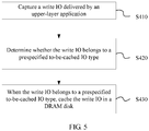
- an embodiment of the present invention provides a write IO procedure of a DRAM-based storage caching method. According to FIG. 5 :
- the caching policy includes write-back (a write-back mode) or write-through (a write-through mode).
- This embodiment of the present invention provides a storage caching technology that is based on a DRAM dynamic random access memory. Based on an existing DRAM memory and a block storage device, the technology has low implementation costs, good scalability, high storage performance for random IOs, and low costs for commercial use. With the technology in this embodiment of the present invention, performance of small-sized random IOs on a terminal device is improved, and a problem of fragmentation of storage space caused by large quantities of random IOs and rewrite operations can also be alleviated. In addition, the technology of the present invention allows differentiated caching for IOs, thereby achieving optimum performance improvement. Finally, this technology can also effectively improve a service life of a flash storage device.
- an embodiment of the present invention provides a write IO procedure of a DRAM-based storage caching method. According to FIG. 6 :
- the caching policy includes write-back (a write-back mode) or write-through (a write-through mode).
- Write-back means that cached data is flushed into a block storage device at a later time, and at a time of a data update, data is written only to the cache cache (the above mentioned DRAM disk). Changed data is not written to the back-end storage until the data is replaced out of the cache.
- This mode is advantageous in a fast writing speed because writing to the storage is not required, while disadvantageous in that once a system power failure occurs before updated data is written to the storage, the data cannot be recovered.
- Write-through means that data is directly written to a bottom-layer block device, and at a time of a data update, data is written to both the cache cache (the above-mentioned DRAM disk) and the back-end storage device.
- This mode is advantageous in ease of operation, while disadvantageous in a low data writing speed because changed data needs to be written also to the storage.
- the write IO procedure may further include the following step.
- a data selection method may be LRU (Least Recently Used, the Least Recently Used algorithm), or may be using continuous dirty data occupying largest space.
- Dirty data is a common technical definition in the database field. To be specific, a file is read into a memory for access; and if the data is not changed, the data is clean, or if the data is changed, the data is dirty data, and needs to be written back to a bottom-layer device, or else the updated data is lost.
- dirty data means that data cached in the DRAM disk is not consistent with data in the block device.
- the write IO procedure may further include the following step.
- determining whether caching into the DRAM disk is required for the IO may be performed based on a size of the IO.
- this may alternatively be performed based on a cold/hot data type of the IO.
- this may be performed based on another policy specifying an IO type, or a decision whether caching into the DRAM disk is required is made based on a storage location of the IO in a back-end device.
- This embodiment of the present invention provides a storage caching technology that is based on a DRAM dynamic random access memory. Based on an existing DRAM memory and a block storage device, the technology has low implementation costs, good scalability, high storage performance for random IOs, and low costs for commercial use. With the technology in this embodiment of the present invention, performance of small-sized random IOs on a terminal device is improved, and a problem of fragmentation of storage space caused by large quantities of random IOs and rewrite operations can also be alleviated. In addition, the technology of the present invention allows differentiated caching for IOs, thereby achieving optimum performance improvement. Finally, this technology can also effectively improve a service life of a flash storage device.
- an embodiment of the present invention provides a write IO procedure of a DRAM-based storage caching method. According to FIG. 7 :
- determining whether the write IO is a hot data IO may be performed according to based on a configuration policy. For example, determining whether the data is cold or hot data may be performed based on a recent access frequency and a type of the write IO. For example, in an embodiment, an IO on a directory file may be considered as hot data. That is, when the write IO is a directory file IO, the write IO is considered to be a hot data IO.
- the caching policy includes write-back (a write-back mode) or write-through (a write-through mode).
- Write-back means that cached data is flushed into a block storage device at a later time, and at a time of a data update, data is written only to the cache cache (the above mentioned DRAM disk). Changed data is not written to the back-end storage until the data is replaced out of the cache.
- This mode is advantageous in a fast writing speed because writing to the storage is not required, while disadvantageous in that once a system power failure occurs before updated data is written to the storage, the data cannot be recovered.
- Write-through means that data is directly written to a bottom-layer block device, and at a time of a data update, data is written to both the cache cache (the above-mentioned DRAM disk) and the back-end storage device.
- This mode is advantageous in ease of operation, while disadvantageous in a low data writing speed because changed data needs to be written also to the storage.
- the write IO is a cold data IO
- the write IO delivered by the upper-layer application is a cold data IO
- the IO is directly delivered to the bottom-layer device, without being cached in the DRAM disk.
- the write IO procedure may further include the following step.
- a data selection method may be LRU (Least Recently Used, the Least Recently Used algorithm), or may be using continuous dirty data occupying largest space. Dirty data is a common technical definition in the database field. To be specific, a file is read into a memory for access; and if the data is not changed, the data is clean, or if the data is changed, the data is dirty data, and needs to be written back to a bottom-layer device, or else the updated data is lost.
- LRU Least Recently Used, the Least Recently Used algorithm
- the write IO procedure may further include the following step.
- determining whether caching into the DRAM disk is required for the IO is performed based on a cold/hot data type of the IO.
- this may be performed based on a size of the IO or another policy specifying an IO type, or a decision whether caching into the DRAM disk is required is made based on a storage location of the IO in a back-end device.
- This embodiment of the present invention provides a storage caching technology that is based on a DRAM dynamic random access memory. Based on an existing DRAM memory and a block storage device, the technology has low implementation costs, good scalability, high storage performance for random IOs, and low costs for commercial use. With the technology in this embodiment of the present invention, performance of small-sized random IOs on a terminal device is improved, and a problem of fragmentation of storage space caused by large quantities of random IOs and rewrite operations can also be alleviated. In addition, the technology of the present invention allows differentiated caching for IOs, thereby achieving optimum performance improvement. Finally, this technology can also effectively improve a service life of a flash storage device.
- DRAM disk caching mechanism implemented by using software in this embodiment of the present invention, performance of small-sized IOs and synchronous write IOs can be significantly improved, so that an overall IO throughput is significantly improved, and a current problem encountered by a terminal that a system runs slower as being used more.
- back erasure and writing by random IOs on a block device such as a flash device can be reduced, thereby reducing an amount of storage space debris, and prolonging a service life of a flash device such as an eMMC.
- an embodiment of the present invention provides a read IO procedure of a DRAM-based storage caching method. According to FIG. 8 :
- determining whether caching into the DRAM disk is required for the IO may be performed based on a cold/hot data type of the IO.
- this may be performed based on a size of the IO or another policy specifying an IO type, or a decision whether caching into the DRAM disk is required is made based on a storage location of the IO in a back-end device. This is not particularly limited in this embodiment of the present invention.
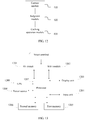
- FIG. 9 The embodiments of the read/write procedures in FIG. 5 , FIG. 6 , FIG. 7 , and FIG. 8 may be vividly depicted in FIG. 9 .
- a brief description is as follows.
- the operations may be specifically performed according to the following steps.
- the normal switch-off is a switch-off performed in accordance with a normal procedure.
- the forced switch-off means a switch-off that is performed not in a normal way, for example, a switch-off caused by low battery or a switch-off caused by unloading of a battery.
- data flushing may be selected or not selected.
- This embodiment of the present invention provides a storage caching technology that is based on a DRAM dynamic random access memory. Based on an existing DRAM memory and a block storage device, the technology has low implementation costs, good scalability, high storage performance for random IOs, and low costs for commercial use. With the technology in this embodiment of the present invention, performance of small-sized random IOs on a terminal device is improved, and a problem of fragmentation of storage space caused by large quantities of random IOs and rewrite operations can also be alleviated. In addition, the technology of the present invention allows differentiated caching for IOs, thereby achieving optimum performance improvement. Finally, this technology can also effectively improve a service life of a flash storage device.
- an embodiment of the present invention provides an application scenario.
- a random IO is cached in a DRAM disk, thereby improving IO performance of a system.
- a part of DRAM space is reserved through pre-configuration, to be used as a DRAM disk.
- a DRAM disk driver creates a block device DRAM disk by using the reserved DRAM space, and binds the DRAM disk to a back-end block device based on a user-preconfiguration policy to form a DRAM disk cache device.
- a user specifies a caching policy for the DRAM disk to be write-back, and sets a type of a to-be-cached IO to a random IO.
- the user delivers an IO.
- the DRAM disk driver captures the IO and determines, based on the configuration policy, whether the IO is a random IO (random IOs are IOs accessing discontinuous storage space addresses, while sequential IOs access continuous block device addresses).
- the DRAM disk bypasses the IO.
- the IO is a random IO, determine a read/write type of the IO.
- IO is a read IO
- search for corresponding data in the DRAM disk search for corresponding data in the DRAM disk; and if the data is found, return the data to an upper layer, or if the data is not found, initiate a read IO request to the back-end block device and cache read data in the DRAM disk.
- IO is a write IO
- search for data corresponding to a block device location in the DRAM disk and if the data is found, overwrite the data, or if the data is not found, write new data into the DRAM disk, and update index management data.
- This embodiment of the present invention provides a storage caching technology that is based on a DRAM dynamic random access memory. Based on an existing DRAM memory and a block storage device, the technology has low implementation costs, good scalability, high storage performance for random IOs, and low costs for commercial use. With the technology in this embodiment of the present invention, performance of small-sized random IOs on a terminal device is improved, and a problem of fragmentation of storage space caused by large quantities of random IOs and rewrite operations can also be alleviated. In addition, the technology of the present invention allows differentiated caching for IOs, thereby achieving optimum performance improvement. Finally, this technology can also effectively improve a service life of a flash storage device.
- DRAM disk caching mechanism implemented by using software in this embodiment of the present invention, performance of small-sized IOs and synchronous write IOs can be significantly improved, so that an overall IO throughput is significantly improved, and a current problem encountered by a terminal that a system runs slower as being used more.
- back erasure and writing by random IOs on a block device such as a flash device can be reduced, thereby reducing an amount of storage space debris, and prolonging a service life of a flash device such as an eMMC.
- an embodiment of the present invention provides an application scenario.
- cold and hot data IOs are cached in a DRAM disk, thereby improving IO performance of a system.
- a part of DRAM space is reserved through pre-configuration, to be used as a DRAM disk.
- a DRAM disk driver creates a block device DRAM disk by using the reserved DRAM space, and binds the DRAM disk to a back-end block device to form a DRAM disk cache device.
- a user specifies a caching policy for the DRAM disk to be write-back, and sets a type of a to-be-cached IO to a hot data IO.
- a policy for differentiating cold and hot data may be user-configured. Classification of cold and hot data includes but is not limited to, directory files and normal files, metadata and normal data, other data types that a service is aware of, and the like.
- the user delivers an IO.
- the DRAM disk driver captures the IO, and determines, based on the configuration policy, whether the IO is a hot data IO.
- the DRAM disk bypasses the IO.
- IO is a read IO
- search for corresponding data in the DRAM disk search for corresponding data in the DRAM disk; and if the data is found, return the data to an upper layer, or if the data is not found, initiate a read IO request to the back-end block device and cache read data in the DRAM disk.
- IO is a write IO
- search for data corresponding to a block device location in the DRAM disk and if the data is found, overwrite the data, or if the data is not found, write new data into the DRAM disk, and update index management data.
- This embodiment of the present invention provides a storage caching technology that is based on a DRAM dynamic random access memory. Based on an existing DRAM memory and a block storage device, the technology has low implementation costs, good scalability, high storage performance for random IOs, and low costs for commercial use. With the technology in this embodiment of the present invention, performance of small-sized random IOs on a terminal device is improved, and a problem of fragmentation of storage space caused by large quantities of random IOs and rewrite operations can also be alleviated. In addition, the technology of the present invention allows differentiated caching for IOs, thereby achieving optimum performance improvement. Finally, this technology can also effectively improve a service life of a flash storage device.
- DRAM disk caching mechanism implemented by using software in this embodiment of the present invention, performance of small-sized IOs and synchronous write IOs can be significantly improved, so that an overall IO throughput is significantly improved, and a current problem encountered by a terminal that a system runs slower as being used more.
- back erasure and writing by random IOs on a block device such as a flash device can be reduced, thereby reducing an amount of storage space debris, and prolonging a service life of a flash device such as an eMMC.
- an embodiment of the present invention provides a terminal provided with a DRAM, and the terminal includes a capture module 410, a judgment module 420, and a caching operation module 430.
- the capture module 410 configured to capture an IO delivered by an upper-layer application.
- the judgment module 420 configured to determine, according to based on a configuration policy, whether the IO captured by the capture module 410 belongs to a to-be-cached IO type.
- determining whether caching into a DRAM disk is required for the IO may be performed based on a size of the IO.
- this may alternatively be performed based on a cold/hot data type of the IO.
- this may be performed based on another policy specifying an IO type, or a decision whether caching into the DRAM disk is required is made based on a storage location of the IO in a back-end device. This is not particularly limited in this embodiment of the present invention.
- the caching operation module 430 performs a corresponding caching operation for the IO in the DRAM disk based on a read/write type of the IO and a preset caching policy.
- the DRAM disk is a block device created by using a reserved part of DRAM space of an operating system, and storage space of the block device is a reserved section of DRAM space in the DRAM.
- the caching policy includes write-back (a write-back mode) or write-through (a write-through mode).
- the judgment module 420 specifically includes:
- the caching operation module 430 specifically includes:
- the caching unit 432 more specifically includes:
- the caching unit 432 is configured to: when the second judgment unit 431 determines that the IO is a read IO, read data operated by the read IO from the bottom-layer storage device of the terminal, and cache the data in the DRAM disk.
- the caching unit 432 more specifically includes:
- the judgment module 420 specifically includes:
- the caching operation module 430 is specifically configured to: when the first judgment unit determines that the IO is a hot data IO or a random IO, and the second judgment unit determines that the IO is a write IO, cache the write IO into the DRAM disk.
- the caching unit 432 more specifically includes:
- the caching operation module 430 is specifically configured to: when the first judgment unit determines that the IO is a hot data IO or a random IO, and the second judgment unit determines that the IO is a read IO, read data operated by the read IO from the bottom-layer storage device of the terminal and cache the data in the DRAM disk.
- the caching unit 432 more specifically includes:
- This embodiment of the present invention provides a storage caching technology that is based on a DRAM dynamic random access memory. Based on an existing DRAM memory and a block storage device, the technology has low implementation costs, good scalability, high storage performance for random IOs, and low costs for commercial use. With the technology in this embodiment of the present invention, performance of small-sized random IOs on a terminal device is improved, and a problem of fragmentation of storage space caused by large quantities of random IOs and rewrite operations can also be alleviated. In addition, the technology of the present invention allows differentiated caching for IOs, thereby achieving optimum performance improvement. Finally, this technology can also effectively improve a service life of a flash storage device.
- DRAM disk caching mechanism implemented by using software in this embodiment of the present invention, performance of small-sized IOs and synchronous write IOs can be significantly improved, so that an overall IO throughput is significantly improved, and a current problem encountered by a terminal that a system runs slower as being used more.
- back erasure and writing by random IOs on a block device such as a flash device can be reduced, thereby reducing an amount of storage space debris, and prolonging a service life of a flash device such as an eMMC.
- FIG. 13 is a schematic structural diagram of a smart terminal according to an embodiment of the present invention.
- the smart terminal includes hardware modules such as an RF circuit 1201, a Wi-Fi module 1202, a display unit 1203, an input unit 1204, a first memory 1205, a second memory 1206, a processor 1207, a power source 1208, and a GPS module 1209.
- the terminal 1200 may be a mobile phone, a tablet computer, a PDA (Personal Digital Assistant, personal digital assistant), a in-vehicle computer, or the like.
- the RF circuit 1201 is configured to send and receive communication signals, and is capable of measuring a distance to an anchor point through radio packet interaction.
- the Wi-Fi module 1202 is configured to connect to a network and scan for a network signal.
- the RF circuit 1201 and/or the Wi-Fi module 1202 may contact with a radio base station to obtain current position coordinates of the smart terminal.
- the display unit 1203 is configured to display a user interaction interface, and the display unit 1203 may be configured to display information entered by a user or information provided to the user, and various menu pages of the smart terminal.
- the display unit 1203 may include a display panel.
- the display panel may be configured in a form of an LCD (Liquid Crystal Display, liquid crystal display), an OLED (Organic Light-Emitting Diode, organic light-emitting diode), or the like.
- the touch panel covers the display panel to form a touch display, and the processor 1207 provides corresponding visual output on the touch display based on a type of a touch event.
- the input unit 1204 may be configured to: receive input digit or character information, receive an interface operation of a user for application switching and generate a switching signal, and generate signal input relevant to user setting and function controlling of the terminal.
- the input unit 1204 may include a touch panel, or referred to as a touchscreen, and may collect touch operations of a user on or near the touchscreen (for example, an operation performed by a user on the touch panel by using any appropriate object or accessory such as a finger or a stylus).
- the touch panel may be implemented in various types, such as a resistive type, a capacitive type, an infrared type, and a surface acoustic wave type.
- the input unit 1204 may further include other input devices.
- the other input devices may include but are not limited to one or more of a physical keyboard, a function key (for example, a volume control key or a power on/off key), a trackball, a mouse, and a joystick, and the like.
- the first memory 1205 stores an operating system of the terminal, a preset quantity of apps, and interface information. It may be understood that the second memory 1206 may be a secondary storage of the terminal 1200, and the first memory 1205 may be a primary storage of the smart terminal, for example, a DRAM.
- the first memory 1205 may be one of an NVRAM non-volatile dynamic random access memory, a DRAM dynamic random memory, an SRAM static random access memory, a flash flash, and the like.
- the operating system running on the smart terminal is usually installed in the first memory 1205.
- the second memory 1206 may be hard disk, an optical disc, a USB flash drive, a floppy disk or tape drive, a cloud server, or the like.
- currently some third-party apps may also be installed in the second memory 1206.
- the processor 1207 is a control center of the smart terminal, connects various parts of the entire terminal by using various interfaces and lines, and runs or executes software programs and/or modules stored in the first memory 1205 and calls data stored in the second memory 1206, to perform various functions of the smart terminal and/or process data.
- the processor 1207 may include one or more processing units.
- the power source 1208 may supply power to the entire terminal, and includes various types of lithium batteries.
- the GPS module 1209 is configured to obtain position coordinates of the smart terminal.
- S1220 Determine, according to based on a configuration policy, whether the IO belongs to a prespecified to-be-cached IO type.
- determining whether caching into a DRAM disk is required for the IO may be performed based on a size of the IO.
- this may alternatively be performed based on a cold/hot data type of the IO.
- this may be performed based on another policy specifying an IO type, or a decision whether caching into the DRAM disk is required is made based on a storage location of the IO in a back-end device. This is not particularly limited in this embodiment of the present invention.
- the IO disk is a block device created by using a reserved part of DRAM space of an operating system, and storage space of the block device is a reserved section of DRAM space in the DRAM.
- the caching policy includes write-back (a write-back mode) or write-through (a write-through mode).
- This embodiment of the present invention provides a storage caching technology that is based on a DRAM dynamic random access memory. Based on an existing DRAM memory and a block storage device, the technology has low implementation costs, good scalability, high storage performance for random IOs, and low costs for commercial use. With the technology in this embodiment of the present invention, performance of small-sized random IOs on a terminal device is improved, and a problem of fragmentation of storage space caused by large quantities of random IOs and rewrite operations can also be alleviated. In addition, the technology of the present invention allows differentiated caching for IOs, thereby achieving optimum performance improvement. Finally, this technology can also effectively improve a service life of a flash storage device.
- the program may be stored in a computer readable storage medium. When the program runs, the processes of the methods in the embodiments are performed.
- the foregoing storage medium may include: a magnetic disc, an optical disc, a read-only memory (Read-Only Memory, ROM), or a random access memory (Random Access Memory, RAM).
Landscapes
- Engineering & Computer Science (AREA)
- Theoretical Computer Science (AREA)
- Physics & Mathematics (AREA)
- General Engineering & Computer Science (AREA)
- General Physics & Mathematics (AREA)
- Human Computer Interaction (AREA)
- Memory System Of A Hierarchy Structure (AREA)
Applications Claiming Priority (2)
| Application Number | Priority Date | Filing Date | Title |
|---|---|---|---|
| CN201610946703.2A CN108008912A (zh) | 2016-11-02 | 2016-11-02 | 一种基于dram的存储缓存方法和智能终端 |
| PCT/CN2017/109136 WO2018082616A1 (fr) | 2016-11-02 | 2017-11-02 | Procédé de mémoire cache basé sur une dram, et terminal intelligent |
Publications (2)
| Publication Number | Publication Date |
|---|---|
| EP3531265A1 true EP3531265A1 (fr) | 2019-08-28 |
| EP3531265A4 EP3531265A4 (fr) | 2019-11-20 |
Family
ID=62048068
Family Applications (1)
| Application Number | Title | Priority Date | Filing Date |
|---|---|---|---|
| EP17866977.6A Ceased EP3531265A4 (fr) | 2016-11-02 | 2017-11-02 | Procédé de mémoire cache basé sur une dram, et terminal intelligent |
Country Status (4)
| Country | Link |
|---|---|
| US (1) | US20190258582A1 (fr) |
| EP (1) | EP3531265A4 (fr) |
| CN (1) | CN108008912A (fr) |
| WO (1) | WO2018082616A1 (fr) |
Families Citing this family (8)
| Publication number | Priority date | Publication date | Assignee | Title |
|---|---|---|---|---|
| US10810123B1 (en) * | 2017-10-25 | 2020-10-20 | EMC IP Holding Company, LLC | Flush strategy for using DRAM as cache media system and method |
| CN109491789A (zh) * | 2018-11-02 | 2019-03-19 | 浪潮电子信息产业股份有限公司 | 一种分布式存储系统业务均衡处理方法、装置及设备 |
| CN111399753B (zh) * | 2019-08-23 | 2022-08-05 | 杭州海康威视系统技术有限公司 | 写入图片的方法和装置 |
| US10802980B1 (en) * | 2020-03-20 | 2020-10-13 | Cloudflare, Inc. | Caching assets in a multiple cache system |
| CN113625938B (zh) * | 2020-05-06 | 2024-07-30 | 华为技术有限公司 | 一种元数据存储方法及其设备 |
| US11366764B2 (en) | 2020-09-29 | 2022-06-21 | International Business Machines Corporation | Managing a least-recently-used data cache with a persistent body |
| CN115525222B (zh) * | 2022-08-30 | 2026-01-16 | 福建升腾资讯有限公司 | 一种块设备的加速方法及终端 |
| CN119806397B (zh) * | 2024-12-04 | 2025-11-07 | 天翼云科技有限公司 | 一种文件存储网关优化缓存刷脏数据的方法及系统 |
Family Cites Families (10)
| Publication number | Priority date | Publication date | Assignee | Title |
|---|---|---|---|---|
| US6922754B2 (en) * | 2002-12-09 | 2005-07-26 | Infabric Technologies, Inc. | Data-aware data flow manager |
| US9390019B2 (en) * | 2006-02-28 | 2016-07-12 | Violin Memory Inc. | Method and apparatus for providing high-performance and highly-scalable storage acceleration |
| CN101739215A (zh) * | 2008-11-19 | 2010-06-16 | 成都市华为赛门铁克科技有限公司 | 一种确定输入输出调度算法的方法及装置 |
| US8996807B2 (en) * | 2011-02-15 | 2015-03-31 | Intelligent Intellectual Property Holdings 2 Llc | Systems and methods for a multi-level cache |
| US9037791B2 (en) * | 2013-01-22 | 2015-05-19 | International Business Machines Corporation | Tiered caching and migration in differing granularities |
| CN103714010B (zh) * | 2013-12-24 | 2017-04-12 | 华为技术有限公司 | 存储设备写入方法及存储设备 |
| US9665153B2 (en) * | 2014-03-21 | 2017-05-30 | Intel Corporation | Selecting a low power state based on cache flush latency determination |
| CN104239226A (zh) * | 2014-10-10 | 2014-12-24 | 浪潮集团有限公司 | 一种采用独立高速缓存的iSCSI存储服务器设计方法 |
| US9886387B2 (en) * | 2015-01-30 | 2018-02-06 | American Megatrends, Inc. | Method and system for performing on-demand data write through based on virtual machine types |
| CN105426127A (zh) * | 2015-11-13 | 2016-03-23 | 浪潮(北京)电子信息产业有限公司 | 一种分布式集群系统的文件存储方法及装置 |
-
2016
- 2016-11-02 CN CN201610946703.2A patent/CN108008912A/zh active Pending
-
2017
- 2017-11-02 EP EP17866977.6A patent/EP3531265A4/fr not_active Ceased
- 2017-11-02 WO PCT/CN2017/109136 patent/WO2018082616A1/fr not_active Ceased
-
2019
- 2019-05-01 US US16/400,319 patent/US20190258582A1/en not_active Abandoned
Also Published As
| Publication number | Publication date |
|---|---|
| EP3531265A4 (fr) | 2019-11-20 |
| CN108008912A (zh) | 2018-05-08 |
| WO2018082616A1 (fr) | 2018-05-11 |
| US20190258582A1 (en) | 2019-08-22 |
Similar Documents
| Publication | Publication Date | Title |
|---|---|---|
| EP3531265A1 (fr) | Procédé de mémoire cache basé sur une dram, et terminal intelligent | |
| US8918581B2 (en) | Enhancing the lifetime and performance of flash-based storage | |
| EP3301584B1 (fr) | Système de stockage, dispositif de gestion de stockage, dispositif de stockage, dispositif de stockage hybride et procédé de gestion de stockage | |
| KR102746577B1 (ko) | 스토리지 장치 및 스토리지 장치를 포함하는 컴퓨팅 장치 | |
| US10416932B2 (en) | Dirty data management for hybrid drives | |
| EP2989536B1 (fr) | Gestion d'accès à un lecteur hybride en mode économie d'énergie | |
| US20120246390A1 (en) | Information processing apparatus, program product, and data writing method | |
| KR101598727B1 (ko) | 메모리 타입들 간에 데이터를 이동하는 기술 | |
| KR20170109133A (ko) | 하이브리드 메모리 장치 및 그의 데이터 관리 방법 | |
| CN112445766A (zh) | 一种终端碎片整理方法、装置以及终端 | |
| CN115421651A (zh) | 固态硬盘的数据处理方法、固态硬盘、电子设备及介质 | |
| CN110554837A (zh) | 易疲劳存储介质的智能交换 | |
| WO2025026114A1 (fr) | Procédé de traitement de stockage, dispositif électronique et support de stockage lisible | |
| CN110968524A (zh) | 数据存储控制方法、装置、存储介质及电子装置 | |
| CN114676092A (zh) | 一种文件管理方法及相关设备 | |
| JP2020046752A (ja) | 記憶装置及び情報処理システム | |
| EP4099177B1 (fr) | Procédé de nettoyage de données invalides, et procédé | |
| US11941246B2 (en) | Memory system, data processing system including the same, and operating method thereof | |
| CN119556864B (zh) | 一种数据管理方法、设备、介质及程序产品 | |
| KR20140113103A (ko) | 호스트 및 메모리 시스템을 포함하는 사용자 시스템의 동작 방법 | |
| CN110955614A (zh) | 文件缓存的回收方法、装置、存储介质及终端 | |
| KR101718888B1 (ko) | 메모리 시스템 및 그것의 가비지 컬렉션 방법 | |
| US9025380B1 (en) | Management of data storage in a non-volatile memory system | |
| CN121166031A (zh) | 数据处理方法、装置、终端及计算机程序产品 | |
| CN120653179A (zh) | 一种写放大抑制方法、装置及存储设备 |
Legal Events
| Date | Code | Title | Description |
|---|---|---|---|
| STAA | Information on the status of an ep patent application or granted ep patent |
Free format text: STATUS: THE INTERNATIONAL PUBLICATION HAS BEEN MADE |
|
| PUAI | Public reference made under article 153(3) epc to a published international application that has entered the european phase |
Free format text: ORIGINAL CODE: 0009012 |
|
| STAA | Information on the status of an ep patent application or granted ep patent |
Free format text: STATUS: REQUEST FOR EXAMINATION WAS MADE |
|
| 17P | Request for examination filed |
Effective date: 20190520 |
|
| AK | Designated contracting states |
Kind code of ref document: A1 Designated state(s): AL AT BE BG CH CY CZ DE DK EE ES FI FR GB GR HR HU IE IS IT LI LT LU LV MC MK MT NL NO PL PT RO RS SE SI SK SM TR |
|
| AX | Request for extension of the european patent |
Extension state: BA ME |
|
| A4 | Supplementary search report drawn up and despatched |
Effective date: 20191017 |
|
| RIC1 | Information provided on ipc code assigned before grant |
Ipc: G06F 3/06 20060101AFI20191011BHEP |
|
| DAV | Request for validation of the european patent (deleted) | ||
| DAX | Request for extension of the european patent (deleted) | ||
| STAA | Information on the status of an ep patent application or granted ep patent |
Free format text: STATUS: EXAMINATION IS IN PROGRESS |
|
| 17Q | First examination report despatched |
Effective date: 20201120 |
|
| REG | Reference to a national code |
Ref country code: DE Ref legal event code: R003 |
|
| STAA | Information on the status of an ep patent application or granted ep patent |
Free format text: STATUS: THE APPLICATION HAS BEEN REFUSED |
|
| 18R | Application refused |
Effective date: 20221201 |