EP3537549A1 - Steckverbinderanordnung - Google Patents
Steckverbinderanordnung Download PDFInfo
- Publication number
- EP3537549A1 EP3537549A1 EP19155403.9A EP19155403A EP3537549A1 EP 3537549 A1 EP3537549 A1 EP 3537549A1 EP 19155403 A EP19155403 A EP 19155403A EP 3537549 A1 EP3537549 A1 EP 3537549A1
- Authority
- EP
- European Patent Office
- Prior art keywords
- deformation
- conductors
- connector
- connector assembly
- outer conductor
- Prior art date
- Legal status (The legal status is an assumption and is not a legal conclusion. Google has not performed a legal analysis and makes no representation as to the accuracy of the status listed.)
- Granted
Links
Images


Classifications
-
- H—ELECTRICITY
- H01—ELECTRIC ELEMENTS
- H01R—ELECTRICALLY-CONDUCTIVE CONNECTIONS; STRUCTURAL ASSOCIATIONS OF A PLURALITY OF MUTUALLY-INSULATED ELECTRICAL CONNECTING ELEMENTS; COUPLING DEVICES; CURRENT COLLECTORS
- H01R9/00—Structural associations of a plurality of mutually-insulated electrical connecting elements, e.g. terminal strips or terminal blocks; Terminals or binding posts mounted upon a base or in a case; Bases therefor
- H01R9/03—Connectors arranged to contact a plurality of the conductors of a multiconductor cable, e.g. tapping connections
- H01R9/05—Connectors arranged to contact a plurality of the conductors of a multiconductor cable, e.g. tapping connections for coaxial cables
-
- H—ELECTRICITY
- H01—ELECTRIC ELEMENTS
- H01R—ELECTRICALLY-CONDUCTIVE CONNECTIONS; STRUCTURAL ASSOCIATIONS OF A PLURALITY OF MUTUALLY-INSULATED ELECTRICAL CONNECTING ELEMENTS; COUPLING DEVICES; CURRENT COLLECTORS
- H01R13/00—Details of coupling devices of the kinds covered by groups H01R12/70 or H01R24/00 - H01R33/00
- H01R13/646—Details of coupling devices of the kinds covered by groups H01R12/70 or H01R24/00 - H01R33/00 specially adapted for high-frequency, e.g. structures providing an impedance match or phase match
- H01R13/6473—Impedance matching
- H01R13/6474—Impedance matching by variation of conductive properties, e.g. by dimension variations
-
- H—ELECTRICITY
- H01—ELECTRIC ELEMENTS
- H01B—CABLES; CONDUCTORS; INSULATORS; SELECTION OF MATERIALS FOR THEIR CONDUCTIVE, INSULATING OR DIELECTRIC PROPERTIES
- H01B11/00—Communication cables or conductors
- H01B11/002—Pair constructions
-
- H—ELECTRICITY
- H01—ELECTRIC ELEMENTS
- H01B—CABLES; CONDUCTORS; INSULATORS; SELECTION OF MATERIALS FOR THEIR CONDUCTIVE, INSULATING OR DIELECTRIC PROPERTIES
- H01B11/00—Communication cables or conductors
- H01B11/18—Coaxial cables; Analogous cables having more than one inner conductor within a common outer conductor
- H01B11/1869—Construction of the layers on the outer side of the outer conductor
-
- H—ELECTRICITY
- H01—ELECTRIC ELEMENTS
- H01B—CABLES; CONDUCTORS; INSULATORS; SELECTION OF MATERIALS FOR THEIR CONDUCTIVE, INSULATING OR DIELECTRIC PROPERTIES
- H01B7/00—Insulated conductors or cables characterised by their form
- H01B7/08—Flat or ribbon cables
- H01B7/0807—Twin conductor or cable
-
- H—ELECTRICITY
- H01—ELECTRIC ELEMENTS
- H01R—ELECTRICALLY-CONDUCTIVE CONNECTIONS; STRUCTURAL ASSOCIATIONS OF A PLURALITY OF MUTUALLY-INSULATED ELECTRICAL CONNECTING ELEMENTS; COUPLING DEVICES; CURRENT COLLECTORS
- H01R11/00—Individual connecting elements providing two or more spaced connecting locations for conductive members which are, or may be, thereby interconnected, e.g. end pieces for wires or cables supported by the wire or cable and having means for facilitating electrical connection to some other wire, terminal, or conductive member, blocks of binding posts
- H01R11/11—End pieces or tapping pieces for wires, supported by the wire and for facilitating electrical connection to some other wire, terminal or conductive member
-
- H—ELECTRICITY
- H01—ELECTRIC ELEMENTS
- H01R—ELECTRICALLY-CONDUCTIVE CONNECTIONS; STRUCTURAL ASSOCIATIONS OF A PLURALITY OF MUTUALLY-INSULATED ELECTRICAL CONNECTING ELEMENTS; COUPLING DEVICES; CURRENT COLLECTORS
- H01R13/00—Details of coupling devices of the kinds covered by groups H01R12/70 or H01R24/00 - H01R33/00
- H01R13/646—Details of coupling devices of the kinds covered by groups H01R12/70 or H01R24/00 - H01R33/00 specially adapted for high-frequency, e.g. structures providing an impedance match or phase match
- H01R13/6473—Impedance matching
-
- H—ELECTRICITY
- H01—ELECTRIC ELEMENTS
- H01R—ELECTRICALLY-CONDUCTIVE CONNECTIONS; STRUCTURAL ASSOCIATIONS OF A PLURALITY OF MUTUALLY-INSULATED ELECTRICAL CONNECTING ELEMENTS; COUPLING DEVICES; CURRENT COLLECTORS
- H01R13/00—Details of coupling devices of the kinds covered by groups H01R12/70 or H01R24/00 - H01R33/00
- H01R13/648—Protective earth or shield arrangements on coupling devices, e.g. anti-static shielding
- H01R13/658—High frequency shielding arrangements, e.g. against EMI [Electro-Magnetic Interference] or EMP [Electro-Magnetic Pulse]
- H01R13/6581—Shield structure
-
- H—ELECTRICITY
- H01—ELECTRIC ELEMENTS
- H01R—ELECTRICALLY-CONDUCTIVE CONNECTIONS; STRUCTURAL ASSOCIATIONS OF A PLURALITY OF MUTUALLY-INSULATED ELECTRICAL CONNECTING ELEMENTS; COUPLING DEVICES; CURRENT COLLECTORS
- H01R13/00—Details of coupling devices of the kinds covered by groups H01R12/70 or H01R24/00 - H01R33/00
- H01R13/648—Protective earth or shield arrangements on coupling devices, e.g. anti-static shielding
- H01R13/658—High frequency shielding arrangements, e.g. against EMI [Electro-Magnetic Interference] or EMP [Electro-Magnetic Pulse]
- H01R13/6591—Specific features or arrangements of connection of shield to conductive members
- H01R13/6592—Specific features or arrangements of connection of shield to conductive members the conductive member being a shielded cable
-
- H—ELECTRICITY
- H01—ELECTRIC ELEMENTS
- H01R—ELECTRICALLY-CONDUCTIVE CONNECTIONS; STRUCTURAL ASSOCIATIONS OF A PLURALITY OF MUTUALLY-INSULATED ELECTRICAL CONNECTING ELEMENTS; COUPLING DEVICES; CURRENT COLLECTORS
- H01R4/00—Electrically-conductive connections between two or more conductive members in direct contact, i.e. touching one another; Means for effecting or maintaining such contact; Electrically-conductive connections having two or more spaced connecting locations for conductors and using contact members penetrating insulation
- H01R4/10—Electrically-conductive connections between two or more conductive members in direct contact, i.e. touching one another; Means for effecting or maintaining such contact; Electrically-conductive connections having two or more spaced connecting locations for conductors and using contact members penetrating insulation effected solely by twisting, wrapping, bending, crimping, or other permanent deformation
- H01R4/18—Electrically-conductive connections between two or more conductive members in direct contact, i.e. touching one another; Means for effecting or maintaining such contact; Electrically-conductive connections having two or more spaced connecting locations for conductors and using contact members penetrating insulation effected solely by twisting, wrapping, bending, crimping, or other permanent deformation by crimping
- H01R4/183—Electrically-conductive connections between two or more conductive members in direct contact, i.e. touching one another; Means for effecting or maintaining such contact; Electrically-conductive connections having two or more spaced connecting locations for conductors and using contact members penetrating insulation effected solely by twisting, wrapping, bending, crimping, or other permanent deformation by crimping for cylindrical elongated bodies, e.g. cables having circular cross-section
Definitions
- the invention relates to a connector assembly with a connector and a cable connected to the connector.
- the cable carries at least one pair of conductors for transmission of one differential signal each.
- the DE 202015000753 U1 shows a connector assembly with a sleeve part.
- a pair of wires for transmitting a differential signal runs in a cable, a pair of wires for transmitting a differential signal, the wires of the wire pair inside the cable have a first mutual distance.
- the two wires of the wire pair run apart from the sheathed cable section towards the connector in an intermediate section until they enter a guide section of the connector in which they have a second mutual distance which is greater than the first mutual distance.
- the present invention seeks to provide a connector assembly for transmission of differential signals with an improved transfer characteristic.
- this object is achieved by a connector assembly having the features of patent claim 1 and by a manufacturing method having the features of patent claim 12.
- the idea underlying the present invention is to improve a connector assembly by a deformation of the outer conductor with respect to various properties.
- electrical properties such as impedance or EMC compatibility can be favorably influenced by deformation.
- the space can be reduced or change or improve the holding forces of a pair of conductors in the connector assembly.
- the deformation is established, the impedance of the connector assembly adjust.
- the impedance can be adjusted by changing the distance between the outer conductor and the conductors of the pair of conductors or the distance between the conductors of the pair of conductors.
- an impurity of the impedance is prevented in the intermediate portion in the connector assembly.
- an impedance in the intermediate portion corresponds to the reference impedance of the connector.
- the reference impedance is often 100 ohms.
- the deformation compensates for a high-impedance impedance before and / or after deformation by means of a low-impedance in the region of the deformation.
- a high impedance is greater than the reference impedance.
- a low impedance is less than the reference impedance.
- the impedance is given as a complex value function of the frequency. It contains the ratio of the amplitudes of sinusoidal alternating voltage to sinusoidal alternating current as well as the shift of the phase angle between these two quantities.
- the deformation initially overcompensates an impedance value of the connector arrangement, as a result of which the high-resistance impedance before and / or after the deformation and the low-impedance in the region of the deformation at least partially cancel each other out.
- the deformation is formed by magnet forming, squeezing, crimping and / or folding.
- squeezing is a particularly easy applicable type of deformation.
- the deformation is formed such that the distance between the outer conductor and the conductors of the conductor pair disappears in a region of the deformation.
- the holding forces of a connector can be increased.
- a smallest inner diameter of the outer conductor in the region of the deformation is less than or equal to a diameter of a conductor in a non-deformed region, if the deformation is formed on an upper or lower side of the outer conductor.
- a largest inner diameter of the outer conductor in the region of the deformation is less than twice a conductor in a non-deformed region, if the deformation is formed on a side surface of the outer conductor.
- the outer conductor has a longitudinal gap in an area outside the deformation.
- the longitudinal gap is formed by wrapping the connector assembly with an outer conductor when the opposite longitudinal edges of the outer conductor are not connected to each other.
- the longitudinal gap is reduced by the deformation or completely closed, so that the outer conductor has no longitudinal gap more. This is made possible by the outer conductor having a smaller circumference after deformation than before deformation.
- the electrical properties, in particular EMC properties, of a connector assembly can be improved.
- the connector assembly in a region outside the deformation on a crimp. Accordingly, the deformation of the connector assembly as described above is not intended as a connection technique between conductors of a cable and plug contacts. Accordingly, it is advantageous to provide a separate connection means between electrical conductors of a cable and plug contacts.
- the deformation is formed on an upper side, on an opposite lower side and / or on a side surface between the upper side and the lower side of the outer conductor.
- the deformation is formed as a bead.
- Beading can be particularly easy to produce using a variety of tools, for example by striking the area of deformation by means of a pointed object.
- the deformation may also be a plane deformation.
- Level deformations can be formed by means of pliers with suitable jaws or by means of magnetic forming.
- the connector assembly 10 comprises a connector 12 and a cable 14 connected to the connector 12. Both the cable 14 and the connector 12 each have at least one pair of conductors 16 for transmitting a differential signal.
- the pair of conductors 16 may be formed in the connector as a plug contact pair. In the cable, the pair of conductors may be formed as a pair of wires.
- the connector assembly 10 has a first portion 18 in the cable. Furthermore, the plug connector arrangement 10 has a second section 20 on the plug connector side. Between the first portion 18 and the second portion 20, an intermediate portion 22 is formed. In this intermediate section 22, the distance between the conductors of the conductor pair 16 increases from the smaller distance of the wires in the first section 18 to the greater distance of the plug contacts in the second section 20th
- the connector assembly 10 has an outer conductor 24 in both the first portion 18 and the second portion 20 and in the intermediate portion 22.
- the distance of the conductors of the conductor pair 16 is marked with W. In the intermediate section 22, the distance of the outer conductor 24 to the conductors of the pair of conductors 16 is marked V.
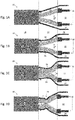
- the Figure 1A shows a connector 10 before the outer conductor 24 has been deformed in the region of the intermediate portion 22.
- FIG. 1B shows a connector assembly 10 with a deformed outer conductor 24.
- the connector assembly 10 according to FIG. 1B Accordingly, in the intermediate portion 22 has a deformation 26, which reduces the distance of the conductors of the pair of conductors 16 to the outer conductor 24.
- the deformation 26 is formed as a planar deformation.
- the connector assembly 10 has a deformation 26 of the outer conductor 24 in the intermediate section 22.
- the deformation 26 is in Figure 1C is formed as a relatively flat bead and reduces the distance between the outer conductor 24 and the pair of conductors 16. Further, the deformation 26 reduces in Figure 1C also the distance between the conductors of the pair of conductors 16 to each other.
- the connector assembly according to FIG. 1D has a deformation 26 of the outer conductor 24 in the intermediate section 22.
- the deformation 26 is formed as a bead. This bead in FIG. 1D is suppressed by the bead is formed such that the outer conductor 24 and the conductors of the conductor pair 16 partially overlap.
- FIG. 2 shows a schematic sectional view of a connector assembly 10 according to an embodiment of the invention.
- FIG. 2 shows a further deformation 26, which is flat.
- FIGS. 3A to 3J each show a cross-sectional view of a connector assembly 10.
- the FIG. 3A shows a cross-sectional view of a connector assembly 10 in an area outside the deformation. Accordingly, in the FIG. 3A to detect any deformation of the outer conductor 24.
- the outer conductor 24 has an upper side 30, an opposite lower side 32 and two side surfaces 34, which are each formed between the upper side 30 and the lower side 32 are on.
- the long sides each form the bottom 32 and the top 30.
- the short sides 34 form the side surfaces.
- FIGS. 3B to 3J each show a cross-sectional view of a connector assembly 10 in a region of deformation 26.
- the deformation 26 is formed as a bead 36 on a bottom 32 of the outer conductor 24.
- the bead 36 reduces the distance V of the outer conductor 24 to the conductors of the pair of conductors 16.
- FIG. 3C a deformation on the top 30 and on the bottom 32 of the connector assembly 10 is shown.
- the deformations on the top 30 and on the bottom 32 are each formed as a bead 36 and reduce in this area the distance V between the conductors of the pair of conductors 16 and the outer conductor 24th
- FIG. 3E shows a planar deformation 38 of the outer conductor 24 on the upper side 30th
- FIG. 3F shows an outer conductor, each with a planar deformation 38 on the top 30 of the outer conductor 24 and on the underside 32nd
- Figure 3G shows a deformation of the outer conductor 24 at its side surfaces 34. Accordingly, the deformation 34 changes the distance W of the conductors of the pair of conductors 16 and the distance V of the outer conductor 24 to the conductors of the pair of conductors sixteenth
- FIGS. 3A to 3G each show an oval outer conductor. However, it is understood that the possibilities of deformation of an outer conductor 24 according to the Figures 3B to 3G also refer to other outer conductor forms.
- Exemplary are further outer conductor forms in the Figures 3H - 3J shown.
- the Figures 3H - 3J show, respectively, a cross-sectional view A of a connector assembly 10 in a non-deformed region and a cross-sectional view B of a connector assembly 10 in a deformed region.
- FIG. 3H shows in the cross-sectional view A a round outer conductor 24 in an undeformed area.
- the connector assembly 10 is shown in a deformed area.
- the deformation is formed as a lateral deformation and reduces the distance W of the conductors of the conductor pair 16 to each other and the distance V of the conductors of the pair of conductors 16 to the outer conductor 24th
- a connector assembly 10 is shown with a round outer conductor 24.
- the outer conductor 24 is deformed to an oval shape. Accordingly, the changes Deformation 26 of FIG. 3I the distance V of the outer conductor 24 to the conductors of the conductor pair 16th
- FIG. 3J shows in the cross-sectional view A a connector assembly 10 with a square outer conductor 24.
- the cross-sectional view B of FIG. 3J Each has a deformation 38 on the upper side 30 and on the lower side 38 of the outer conductor 24.
- FIG. 4A shows a connector assembly 10 in a cross-sectional view in an undeformed area or before deformation.
- the connector assembly 10 in FIG. 4A has an outer conductor 24 which is wound around the insulating part 101 of the connector assembly 10. Accordingly, the outer conductor 24 in FIG. 4A two opposite longitudinal edges 103 and 104 on. Between the opposite longitudinal edges 103 and 104 is a longitudinal gap 28th
- FIGS. 4B and 4C show a connector assembly 10 in a cross-sectional view in a region of deformation after the longitudinal gap 28 in FIG. 4A was closed by a deformation 26.
- the deformation is formed as a planar deformation 38.
- the deformation is formed as a bead 36.
- the outer conductor 24 has been deformed until its opposite edges 103 and 104 overlap each other. It can be provided to fasten the opposing edges 103 and 104 to one another using a connection technique, for example by means of a joining technique, in particular welding.
- FIG. 5 shows in the view A a further schematic representation of the outer conductor 24 of a connector assembly prior to deformation and in the view B after a longitudinal gap 28 has been closed by means of a deformation.
- FIG. 5 shows the outer conductor 24, wherein the outer conductor 24 is deformed in the intermediate portion 22 such that the gap 28 overlap between the opposite longitudinal edges 103 and 104 of the outer conductor 24.
Landscapes
- Details Of Connecting Devices For Male And Female Coupling (AREA)
- Insulated Conductors (AREA)
Abstract
Description
- Die Erfindung betrifft eine Steckverbinderanordnung mit einem Steckverbinder und ein an dem Steckverbinder angeschlossenes Kabel. Das Kabel führt mindestens ein Leiterpaar zur Übertragung von jeweils einem differenziellen Signal.
- Die
DE 202015000753 U1 zeigt eine Steckverbinderanordnung mit einem Hülsenteil. Dabei verläuft in einem Kabel ein Aderpaar zur Übertragung eines differenziellen Signals, wobei die Adern des Aderpaars im Inneren des Kabels einen ersten gegenseitigen Abstand haben. Die beiden Adern des Aderpaars laufen ausgehend von dem ummantelten Kabelabschnitt in Richtung auf den Steckverbinder in einem Zwischenabschnitt auseinander, bis sie in einen Führungsabschnitt des Steckverbinders einlaufen, in dem sie einen zweiten gegenseitigen Abstand haben, der größer ist als der erste gegenseitige Abstand. - Aufgrund der Abstandsänderung zwischen den Adern ändert sich deren differenzielle Impedanz, wodurch es zu einer Störstelle kommen kann.
- Dies ist ein Zustand, den es zu verbessern gilt.
- Vor diesem Hintergrund liegt der vorliegenden Erfindung die Aufgabe zugrunde, eine Steckverbinderanordnung zur Übertragung von differenziellen Signalen mit einer verbesserten Übertragungscharakteristik anzugeben.
- Erfindungsgemäß wird diese Aufgabe durch eine Steckverbinderanordnung mit den Merkmalen des Patentanspruchs 1 sowie durch ein Herstellungsverfahren mit den Merkmalen des Patentanspruchs 12 gelöst.
- Demgemäß ist vorgesehen:
- Steckverbinderanordnung mit einem Steckverbinder und einem an den Steckverbinder angeschlossenem Kabel, welche jeweils wenigstens ein Leiterpaar mit einem ersten und zweiten Leiter zur Übertragung eines differenziellen Signals aufweisen, wobei das Kabel einen ersten Abschnitt aufweist und der Steckverbinder einen zweiten Abschnitt aufweist, in dem das Leiterpaar Steckkontakte aufweist, wobei an einem steckverbinderseitigen Ende des ersten Abschnittes das Kabel an dem Steckverbinder befestigt ist und die Leiter des Leiterpaares des Kabels an den Leitern des Steckverbinders an einem kabelseitigen Ende des zweiten Abschnittes befestigt sind, wobei zwischen dem ersten Abschnitt und dem zweiten Abschnitt ein Zwischenabschnitt ausgebildet ist, wobei das Leiterpaar in dem Zwischenabschnitt und, insbesondere in dem ersten Abschnitt und/oder in dem zweiten Abschnitt, von einem Außenleiter umgeben ist, und wobei der Außenleiter in zumindest einem Teil des Zwischenabschnitts eine Verformung aufweist, die einen Abstand (V) zwischen dem Außenleiter und den Leitern und/oder einen Abstand (W) zwischen den Leitern in einem Bereich der Verformung verringert; sowie
- Herstellungsverfahren für eine Steckverbinderanordnung mit den folgenden Schritten: Bereitstellen einer Steckverbinderanordnung mit einem Steckverbinder und einem an den Steckverbinder angeschlossenem Kabel, welche jeweils wenigstens ein Leiterpaar zur Übertragung eines differenziellen Signals aufweisen, wobei das Kabel einen ersten Abschnitt aufweist und der Steckverbinder einen zweiten Abschnitt aufweist, in dem das Leiterpaar Steckkontakte aufweist, wobei an einem steckverbinderseitigen Ende des ersten Abschnittes das Kabel an dem Steckverbinder befestigt ist und die Leiter des Leiterpaares des Kabels an den Leitern des Steckverbinders an einem kabelseitigen Ende des zweiten Abschnittes befestigt sind, wobei zwischen dem ersten Abschnitt und dem zweiten Abschnitt ein Zwischenabschnitt ausgebildet ist, wobei das Leiterpaar in dem Zwischenabschnitt und, insbesondere in dem ersten Abschnitt und/oder in dem zweiten Abschnitt, von einem Außenleiter umgeben ist; Verformen des Außenleiters in zumindest einem Teil des Zwischenabschnitts.
- Die der vorliegenden Erfindung zugrundeliegende Idee besteht darin, eine Steckverbinderanordnung durch eine Verformung des Außenleiters hinsichtlich verschiedener Eigenschaften zu verbessern. Beispielsweise lassen sich elektrische Eigenschaften wie die Impedanz oder die EMV-Verträglichkeit durch eine Verformung günstig beeinflussen. Ferner lässt sich auch der Bauraum reduzieren oder verändern bzw. die Haltekräfte eines Leiterpaares in der Steckverbinderanordnung verbessern.
- Vorteilhafte Ausgestaltungen und Weiterbildungen ergeben sich aus den weiteren Unteransprüchen sowie aus der Beschreibung unter Bezugnahme auf die Figuren der Zeichnung.
- Gemäß einer bevorzugten Ausführungsform der Erfindung ist die Verformung eingerichtet, die Impedanz der Steckverbinderanordnung einzustellen. Die Impedanz lässt sich einstellen, indem der Abstand zwischen dem Außenleiter und den Leitern des Leiterpaares oder der Abstand zwischen den Leitern des Leiterpaares verändert wird.
- Dementsprechend kann vorgesehen sein, dass eine Störstelle der Impedanz in dem Zwischenabschnitt in der Steckverbinderanordnung verhindert wird. In diesem Fall entspricht eine Impedanz in dem Zwischenabschnitt der Bezugsimpedanz des Steckverbinders. Die Bezugsimpedanz beträgt häufig 100 Ohm.
- Alternativ ist es zweckmäßig, dass die Verformung eine hochohmige Impedanz vor und/oder nach der Verformung durch eine niederohmige Impedanz im Bereich der Verformung kompensiert. Eine hochohmige Impedanz ist größer als die Bezugsimpedanz. Eine niederohmige Impedanz ist kleiner als die Bezugsimpedanz.
- Die Impedanz wird als komplexwertige Funktion der Frequenz angegeben. Sie beinhaltet das Verhältnis der Amplituden von sinusförmiger Wechselspannung zu sinusförmigem Wechselstrom sowie die Verschiebung der Phasenwinkel zwischen diesen beiden Größen.
- Dementsprechend kann vorgesehen sein, dass die Verformung einen Impedanzwert der Steckverbinderanordnung zunächst überkompensiert, wodurch sich die hochohmige Impedanz vor und/oder nach der Verformung und die niederohmige Impedanz im Bereich der Verformung zumindest teilweise gegenseitig aufheben.
- Gemäß einer bevorzugten Weiterbildung der Erfindung ist die Verformung durch Magnetumformen, Quetschen, Kräuseln und/oder Falten ausgebildet. Besonders das Quetschen ist eine besonders einfache anwendbare Art der Verformung.
- Gemäß einer bevorzugten Weiterbildung der Erfindung ist die Verformung derart ausgebildet, dass der Abstand zwischen dem Außenleiter und den Leitern des Leiterpaares in einem Bereich der Verformung verschwindet. In diesem Fall spricht man von einem Überdrücken des Außenleiters durch die Verformung, sofern die Verformung durch Quetschen gebildet wurde.
- Somit lassen sich beispielsweise auch die Haltekräfte eines Steckverbinders erhöhen.
- Diesbezüglich ist es zweckmäßig wenn ein kleinster Innendurchmesser des Außenleiters im Bereich der Verformung geringer oder gleich ist als ein Durchmesser eines Leiters in einem nicht verformten Bereich, wenn die Verformung an einer Ober- oder Unterseite des Außenleiters ausgebildet ist.
- Alternativ oder zusätzlich kann es zweckmäßig sein wenn ein größter Innendurchmesser des Außenleiters im Bereich der Verformung geringer ist als das zweifache eines Leiters in einem nicht verformten Bereich, wenn die Verformung an einer Seitenfläche des Außenleiters ausgebildet ist.
- Dementsprechend wird auch von einem Überdrücken des Außenleiters gesprochen. Auf diese Weise lässt sich eine hochohmige Impedanz, bezogen auf die Bezugsimpedanz, außerhalb der Verformung durch eine niederohmige Impedanz, bezogen auf die Bezugsimpedanz, im Bereich der Verformung überkompensieren.
- Gemäß einer bevorzugten Weiterbildung der Erfindung weist der Außenleiter in einem Bereich außerhalb der Verformung einen Längsspalt auf. Der Längsspalt entsteht durch umwickeln der Steckverbinderanordnung mit einem Außenleiter, wenn die gegenüberliegenden Längskanten des Außenleiters nicht miteinander verbunden werden.
- Auf diese Weise lassen sich die Herstellungskosten eines Steckverbinders reduzieren.
- Dabei ist es insbesondere zweckmäßig, wenn der Längsspalt durch die Verformung verkleinert oder vollständig geschlossen ist, so dass der Außenleiter keinen Längsspalt mehr aufweist. Dies wird ermöglicht, indem der Außenleiter nach der Verformung einen geringeren Umfang als vor der Verformung aufweist. Somit lassen sich die elektrischen Eigenschaften, insbesondere EMV-Eigenschaften, einer Steckverbinderanordnung verbessern.
- Gemäß einer bevorzugten Weiterbildung der Erfindung weist die Steckverbinderanordnung in einem Bereich außerhalb der Verformung einen Crimp auf. Dementsprechend ist die Verformung der Steckverbinderanordnung, wie sie vorstehend beschrieben wurde, eher nicht als Verbindungstechnik zwischen Leitern eines Kabels und Steckkontakten vorgesehen. Dementsprechend ist es vorteilhaft, ein gesondertes Verbindungsmittel zwischen elektrischen Leitern eines Kabels und Steckkontakten vorzusehen.
- Gemäß einer bevorzugten Weiterbildung der Erfindung ist die Verformung an einer Oberseite, an einer gegenüberliegenden Unterseite und/oder an einer Seitenfläche zwischen der Oberseite und der Unterseite des Außenleiters ausgebildet.
- Eine Oberseite, eine Unterseite und Seitenflächen sind in dieser Patentanmeldung in den Zeichnungen sowie der zugehörigen Beschreibung definiert.
- Gemäß einer bevorzugten Weiterbildung der Erfindung ist die Verformung als Sicke ausgebildet. Sicken lassen sich mittels vielfältiger Werkzeuge besonders einfach herstellen, beispielsweise indem mittels eines spitzen Gegenstands auf den Bereich der Verformung geschlagen wird.
- Alternativ oder zusätzlich dazu kann die Verformung auch eine ebene Verformung sein. Ebene Verformungen lassen sich Beispiels mittels Zangen mit geeigneten Backen oder mittels Magnetumformung ausbilden.
- Es versteht sich, dass die voranstehend genannten und die nachstehend noch zu erläuternden Merkmale nicht nur in der jeweils angegebenen Kombination, sondern auch in anderen Kombinationen oder in Alleinstellung verwendbar sind, ohne den Rahmen der vorliegenden Erfindung zu verlassen.
- Die obigen Ausgestaltungen und Weiterbildungen lassen sich, sofern sinnvoll, beliebig miteinander kombinieren. Weitere mögliche Ausgestaltungen, Weiterbildungen und Implementierungen der Erfindung umfassen auch nicht explizit genannte Kombinationen von zuvor oder im Folgenden bezüglich der Ausführungsbeispiele beschriebenen Merkmale der Erfindung. Insbesondere wird dabei der Fachmann auch Einzelaspekte als Verbesserungen oder Ergänzungen zu der jeweiligen Grundform der vorliegenden Erfindung hinzufügen.
- Die vorliegende Erfindung wird nachfolgend anhand der in den schematischen Figuren der Zeichnung angegebenen Ausführungsbeispiele näher erläutert. Es zeigen dabei:
- Fig. 1A
- eine Längsschnittdarstellung einer Ausführungsform der Erfindung;
- Fig. 1B
- eine Längsschnittdarstellung einer Ausführungsform der Erfindung;
- Fig. 1C
- eine Längsschnittdarstellung einer Ausführungsform der Erfindung;
- Fig. 1D
- eine Längsschnittdarstellung einer Ausführungsform der Erfindung;
- Fig. 2
- eine Längsschnittdarstellung einer weiteren Ausführungsform der Erfindung;
- Fig. 3A
- eine Querschnittdarstellung einer Ausführungsform der Erfindung;
- Fig. 3B
- eine Querschnittdarstellung einer Ausführungsform der Erfindung;
- Fig. 3C
- eine Querschnittdarstellung einer Ausführungsform der Erfindung;
- Fig. 3D
- eine Querschnittdarstellung einer Ausführungsform der Erfindung;
- Fig. 3E
- eine Querschnittdarstellung einer Ausführungsform der Erfindung;
- Fig. 3F
- eine Querschnittdarstellung einer Ausführungsform der Erfindung;
- Fig. 3G
- eine Querschnittdarstellung einer Ausführungsform der Erfindung;
- Fig. 3H
- eine Querschnittdarstellung einer Ausführungsform der Erfindung;
- Fig. 3I
- eine Querschnittdarstellung einer Ausführungsform der Erfindung;
- Fig. 3J
- eine Querschnittdarstellung einer Ausführungsform der Erfindung;
- Fig. 4A
- eine Querschnittdarstellung einer Ausführungsform der Erfindung;
- Fig. 4B
- eine Querschnittdarstellung einer Ausführungsform der Erfindung;
- Fig. 4C
- eine Querschnittdarstellung einer Ausführungsform der Erfindung;
- Fig. 5
- eine Längsschnittdarstellung einer Ausführungsform der Erfindung;
- Die beiliegenden Figuren der Zeichnung sollen ein weiteres Verständnis der Ausführungsformen der Erfindung vermitteln. Sie veranschaulichen Ausführungsformen und dienen im Zusammenhang mit der Beschreibung der Erklärung von Prinzipien und Konzepten der Erfindung. Andere Ausführungsformen und viele der genannten Vorteile ergeben sich im Hinblick auf die Zeichnungen. Die Elemente der Zeichnungen sind nicht notwendigerweise maßstabsgetreu zueinander gezeigt.
- In den Figuren der Zeichnung sind gleiche, funktionsgleiche und gleich wirkende Elemente, Merkmale und Komponenten - sofern nichts anderes ausgeführt ist - jeweils mit denselben Bezugszeichen versehen.
- Im Folgenden werden die Figuren zusammenhängend und übergreifend beschrieben.
- Die
Figuren 1A, 1B, 1C und 1D zeigen jeweils eine schematische Schnittsicht einer Steckverbinderanordnung 10. Die Steckverbinderanordnung 10 umfasst einen Steckverbinder 12 und ein an den Steckverbinder 12 angeschlossenes Kabel 14. Sowohl das Kabel 14 als auch der Steckverbinder 12 weisen jeweils wenigstens ein Leiterpaar 16 zur Übertragung eines differenziellen Signals auf. Das Leiterpaar 16 kann in dem Steckverbinder als Steckkontaktpaar ausgebildet sein. In dem Kabel kann das Leiterpaar als Aderpaar ausgebildet sein. - Die Steckverbinderanordnung 10 weist in dem Kabel einen ersten Abschnitt 18 auf. Ferner weist die Steckverbinderanordnung 10 steckverbinderseitig einen zweiten Abschnitt 20 auf. Zwischen dem ersten Abschnitt 18 und dem zweiten Abschnitt 20 ist ein Zwischenabschnitt 22 ausgebildet. In diesem Zwischenabschnitt 22 vergrößert sich der Abstand der Leiter des Leiterpaares 16 von dem geringeren Abstand der Adern in dem ersten Abschnitt 18 auf den größeren Abstand der Steckkontakte in dem zweiten Abschnitt 20.
- Die Steckverbinderanordnung 10 weist sowohl in dem ersten Abschnitt 18 als auch in dem zweiten Abschnitt 20 und in dem Zwischenabschnitt 22 einen Außenleiter 24 auf.
- In dem Zwischenabschnitt 22 ist der Abstand der Leiter des Leiterpaares 16 mit W gekennzeichnet. In dem Zwischenabschnitt 22 ist der Abstand des Außenleiters 24 zu den Leitern des Leiterpaares 16 mit V gekennzeichnet.
- Die
Figur 1A zeigt einen Steckverbinder 10, bevor der Außenleiter 24 in dem Bereich des Zwischenabschnittes 22 verformt wurde. - Die
Figur 1B zeigt eine Steckverbinderanordnung 10 mit einem verformten Außenleiter 24. Die Steckverbinderanordnung 10 gemäßFigur 1B weist dementsprechend in dem Zwischenabschnitt 22 eine Verformung 26 auf, die den Abstand der Leiter des Leiterpaares 16 zu dem Außenleiter 24 verringert. Die Verformung 26 ist als ebene Verformung ausgebildet. - Die Steckverbinderanordnung 10 gemäß
Figur 1C weist in dem Zwischenabschnitt 22 eine Verformung 26 des Außenleiters 24 auf. Die Verformung 26 ist inFigur 1C als relativ flache Sicke ausgebildet und verringert den Abstand zwischen dem Außenleiter 24 und dem Leiterpaar 16. Ferner verringert die Verformung 26 inFigur 1C auch den Abstand der Leiter des Leiterpaares 16 zueinander. - Die Steckverbinderanordnung gemäß
Figur 1D weist eine Verformung 26 des Außenleiters 24 in dem Zwischenabschnitt 22 auf. Die Verformung 26 ist als Sicke ausgebildet. Diese Sicke inFigur 1D ist überdrückt, indem die Sicke derart geformt ist, dass sich der Außenleiter 24 und die Leiter des Leiterpaares 16 teilweise überlappen. -
Figur 2 zeigt eine schematische Schnittsicht einer Steckverbinderanordnung 10 gemäß einer Ausführungsform der Erfindung.Figur 2 zeigt eine weitere Verformung 26, welche eben ausgebildet ist. - Die
Figuren 3A bis 3J zeigen jeweils eine Querschnittsicht einer Steckverbinderanordnung 10. DieFigur 3A zeigt eine Querschnittsicht einer Steckverbinderanordnung 10 in einem Bereich außerhalb der Verformung. Dementsprechend ist in derFigur 3A keine Verformung des Außenleiters 24 zu erkennen. Der Außenleiter 24 weist eine Oberseite 30, eine gegenüberliegende Unterseite 32 und zwei Seitenflächen 34, die jeweils zwischen der Oberseite 30 und der Unterseite 32 ausgebildet sind, auf. Bei Steckverbinderanordnungen mit verschiedenen Seitenlängen bilden in dieser Patentanmeldung die langen Seiten jeweils die Unterseite 32 bzw. die Oberseite 30. Die kurzen Seiten 34 bilden die Seitenflächen. - Die
Figuren 3B bis 3J zeigen jeweils eine Querschnittsicht einer Steckverbinderanordnung 10 in einem Bereich einer Verformung 26. - In der
Figur 3B ist die Verformung 26 als Sicke 36 auf einer Unterseite 32 des Außenleiters 24 ausgebildet. InFigur 3B verringert die Sicke 36 den Abstand V des Außenleiters 24 zu den Leitern des Leiterpaares 16. - In
Figur 3C ist eine Verformung auf der Oberseite 30 sowie auf der Unterseite 32 der Steckverbinderanordnung 10 dargestellt. Die Verformungen auf der Oberseite 30 und auf der Unterseite 32 sind jeweils als Sicke 36 ausgebildet und verringern in diesem Bereich den Abstand V zwischen den Leitern des Leiterpaares 16 und dem Außenleiter 24. - In
Figur 3D ist der Außenleiter 24 derart verformt, dass dieser zu dem Isolierteil 101 weitgehend konturfolgend ist. Dementsprechend ist der Abstand zwischen dem Außenleiter 24 und den Leitern des Leiterpaares 16 verringert. Eine derartige Verformung lässt sich beispielsweise mittels Magnetumformung herstellen. Dementsprechend verändert die Verformung ausFigur 3D den Abstand V des Außenleiters 24 zu den Leitern des Leiterpaares 16 sowie den Abstand W der Leiter des Leiterpaares 16 zueinander. -
Figur 3E zeigt eine ebene Verformung 38 des Außenleiters 24 auf dessen Oberseite 30. -
Figur 3F zeigt einen Außenleiter mit jeweils einer ebenen Verformung 38 auf der Oberseite 30 des Außenleiters 24 sowie auf dessen Unterseite 32. -
Figur 3G zeigt eine Verformung des Außenleiters 24 an dessen Seitenflächen 34. Dementsprechend verändert die Verformung 34 den Abstand W der Leiter des Leiterpaares 16 sowie den Abstand V des Außenleiters 24 zu den Leitern des Leiterpaares 16. - Die
Figuren 3A bis 3G zeigen jeweils einen ovalen Außenleiter. Es versteht sich jedoch, dass sich die Möglichkeiten der Verformung eines Außenleiters 24 gemäß denFiguren 3B bis 3G auch auf andere Außenleiterformen beziehen. - Exemplarisch sind weitere Außenleiterformen in den
Figuren 3H - 3J dargestellt. DieFiguren 3H - 3J zeigen jeweils eine Querschnittsicht A einer Steckverbinderanordnung 10 in einem nicht verformten Bereich sowie eine Querschnittsicht B einer Steckverbinderanordnung 10 in einem verformten Bereich. - Die
Figur 3H zeigt in der Querschnittsicht A einen runden Außenleiter 24 in einem nicht verformten Bereich. In der Querschnittsicht B derFigur 3H ist die Steckverbinderanordnung 10 in einem verformten Bereich dargestellt. Die Verformung ist als seitliche Verformung ausgebildet und verringert den Abstand W der Leiter des Leiterpaares 16 zueinander sowie den Abstand V der Leiter des Leiterpaares 16 zu dem Außenleiter 24. - In der Querschnittsicht A der
Figur 3I ist eine Steckverbinderanordnung 10 mit einem runden Außenleiter 24 dargestellt. In der Querschnittsicht B derFigur 3I ist der Außenleiter 24 zu einer ovalen Form verformt. Dementsprechend ändert die Verformung 26 derFigur 3I den Abstand V des Außenleiters 24 zu den Leitern des Leiterpaares 16. - Die
Figur 3J zeigt in der Querschnittsicht A eine Steckverbinderanordnung 10 mit einem quadratischen Außenleiter 24. Die Querschnittsicht B derFigur 3J weist jeweils eine Verformung 38 an der Oberseite 30 sowie an der Unterseite 38 des Außenleiters 24 auf. - Die
Figur 4A zeigt eine Steckverbinderanordnung 10 in einer Querschnittsicht in einem nicht verformten Bereich bzw. vor dem Verformen. Die Steckverbinderanordnung 10 inFigur 4A weist einen Außenleiter 24 auf, welcher um das Isolierteil 101 der Steckverbinderanordnung 10 gewickelt ist. Dementsprechend weist der Außenleiter 24 inFigur 4A zwei gegenüberliegende Längskanten 103 und 104 auf. Zwischen den gegenüberliegenden Längskanten 103 und 104 befindet sich ein Längsspalt 28. - Die
Figuren 4B und 4C zeigen eine Steckverbinderanordnung 10 in einer Querschnittsicht in einem Bereich der Verformung, nachdem der Längsspalt 28 gemäßFigur 4A durch eine Verformung 26 geschlossen wurde. - In den
Figuren 4B und 4C wurde der Längsspalt 28 jeweils geschlossen, indem der Abstand V zwischen den Leitern des Leiterpaares 16 und dem Außenleiter 24 jeweils verringert wurde. - In
Figur 4B ist die Verformung als ebene Verformung 38 ausgebildet. - In
Figur 4C ist die Verformung als Sicke 36 ausgebildet. - In beiden
Figuren 4B und 4C wurde der Außenleiter 24 so weit verformt, bis dessen gegenüberliegende Kanten 103 und 104 sich jeweils überlappen bzw. berühren. Es kann vorgesehen sein, die gegenüberliegenden Kanten 103 und 104 mit einer Verbindungstechnik aneinander zu befestigen, beispielsweise mittels einer Fügetechnik, insbesondere Verschweißen. -
Figur 5 zeigt in der Ansicht A eine weitere schematische Darstellung des Außenleiters 24 einer Steckverbinderanordnung vor einer Verformung sowie in der Ansicht B nach dem ein Längsspalt 28 mittels einer Verformung geschlossen wurde. - In der Ansicht A der
Figur 5 ist ersichtlich, dass in dem Zwischenabschnitt 22 ein Längsspalt 28 zwischen gegenüberliegenden Längskanten 103 und 104 des Außenleiters 24 gebildet ist. Der Längsspalt 28 erstreckt sich ausschließlich über den Zwischenabschnitt 22. - Ansicht B der
Figur 5 zeigt den Außenleiter 24, wobei der Außenleiter 24 im Zwischenabschnitt 22 derart verformt ist, dass sich der Spalt 28 zwischen den gegenüberliegenden Längskanten 103 und 104 des Außenleiters 24 überlappen. - Die Erfindung ist nicht auf die dargestellten Ausführungsformen, Ausprägungen und Untervarianten beschränkt. Von der Erfindung sind insbesondere alle Kombinationen der in den einzelnen Patentansprüchen jeweils beanspruchten Merkmale, der in der Beschreibung jeweils offenbarten Merkmale und der in den Figuren der Zeichnung jeweils dargestellten Merkmale mit abgedeckt, soweit sie technisch sinnvoll sind.
- Obwohl die vorliegende Erfindung anhand bevorzugter Ausführungsbeispiele vorstehend vollständig beschrieben wurde, ist sie darauf nicht beschränkt, sondern auf vielfältige Art und Weise modifizierbar.
-
- 10
- Steckverbinderanordnung
- 12
- Steckverbinder
- 14
- Kabel
- 16
- Leiterpaar
- 18
- erster Abschnitt
- 20
- zweiter Abschnitt
- 22
- Zwischenabschnitt
- 24
- Außenleiter
- 26
- Verformung
- 28
- Längsspalt
- 30
- Oberseite
- 32
- Unterseite
- 34
- Seitenfläche
- 36
- Sicke
- 38
- Verformung
- 103 und 104
- gegenüberliegenden Längskanten / Kanten
- V
- Abstand zwischen dem Außenleiter und den Leitern
- W
- Abstand zwischen den Leitern in einem Bereich der Verformung
Claims (14)
- Steckverbinderanordnung (10) mit einem Steckverbinder (12) und einem an den Steckverbinder angeschlossenem Kabel (14), welche jeweils wenigstens ein Leiterpaar (16) mit einem ersten und zweiten Leiter zur Übertragung eines differenziellen Signals aufweisen,
wobei das Kabel einen ersten Abschnitt (18) aufweist und der Steckverbinder einen zweiten Abschnitt (20) aufweist, in dem das Leiterpaar Steckkontakte aufweist,
wobei an einem steckverbinderseitigen Ende des ersten Abschnittes das Kabel an dem Steckverbinder befestigt ist und die Leiter des Leiterpaares des Kabels an den Leitern des Steckverbinders an einem kabelseitigen Ende des zweiten Abschnittes befestigt sind,
wobei zwischen dem ersten Abschnitt und dem zweiten Abschnitt ein Zwischenabschnitt (22) ausgebildet ist,
wobei das Leiterpaar in dem Zwischenabschnitt und, insbesondere in dem ersten Abschnitt und/oder in dem zweiten Abschnitt, von einem Außenleiter (24) umgeben ist, und
wobei der Außenleiter in zumindest einem Teil des Zwischenabschnitts eine Verformung (26) aufweist, die einen Abstand (V) zwischen dem Außenleiter und den Leitern und/oder einen Abstand (W) zwischen den Leitern in einem Bereich der Verformung verringert. - Steckverbinderanordnung nach Anspruch 1, wobei die Verformung eingerichtet ist, die Impedanz der Steckverbinderanordnung einzustellen.
- Steckverbinderanordnung nach Anspruch 2, wobei die Verformung eine hochohmige Impedanz, bezogen auf die Bezugsimpedanz, vor und/oder nach der Verformung durch eine niederohmige Impedanz, bezogen auf die Bezugsimpedanz, im Bereich der Verformung kompensiert.
- Steckverbinderanordnung nach einem der vorstehenden Ansprüche, wobei die Verformung durch Magnetumformen, Quetschen, Kräuseln und/oder Falten ausgebildet ist.
- Steckverbinderanordnung nach einem der vorstehenden Ansprüche, wobei der Abstand zwischen dem Außenleiter und den Leitern in einem Bereich der Verformung null ist.
- Steckverbinderanordnung nach einem der vorstehenden Ansprüche, wobei der Abstand zwischen den Leitern in einem Bereich der Verformung null ist.
- Steckverbinderanordnung nach Anspruch 5 und 6, wobei ein kleinster Durchmesser des Außenleiters im Bereich der Verformung geringer ist als ein Durchmesser eines Leiters in einem nicht verformten Bereich und/oder wobei ein größter Durchmesser des Außenleiters im Bereich der Verformung geringer ist als das zweifache eines Leiters in einem nicht verformten Bereich.
- Steckverbinderanordnung nach einem der vorstehenden Ansprüche, wobei der Außenleiter in einem Bereich außerhalb der Verformung einen Längsspalt (28) aufweist.
- Steckverbinderanordnung nach einem der vorstehenden Ansprüche, wobei ein Längsspalt in dem Bereich der Verformung verkleinert oder geschlossen ist.
- Steckverbinderanordnung nach einem der vorstehenden Ansprüche, welche in einem Bereich außerhalb der Verformung einen Crimp aufweist.
- Steckverbinderanordnung nach einem der vorstehenden Ansprüche, wobei die Verformung an einer Oberseite (30) und/oder an einer gegenüberliegenden Unterseite (32) und/oder an einer Seitenfläche (34) zwischen der Ober- und Unterseite des Außenleiters ausgebildet ist.
- Steckverbinderanordnung nach einem der vorstehenden Ansprüche, wobei die Verformung als Sicke (36) ausgebildet ist.
- Steckverbinderanordnung nach einem der vorstehenden Ansprüche, wobei die Verformung eine ebene Verformung (38) ist.
- Herstellungsverfahren für eine Steckverbinderanordnung mit den folgenden Schritten:- Bereitstellen einer Steckverbinderanordnung mit einem Steckverbinder (12) und einem an den Steckverbinder angeschlossenem Kabel (14), welche jeweils wenigstens ein Leiterpaar (16) zur Übertragung eines differenziellen Signals aufweisen, wobei das Kabel einen ersten Abschnitt (18) aufweist und der Steckverbinder einen zweiten Abschnitt (20) aufweist, in dem das Leiterpaar Steckkontakte aufweist, wobei an einem steckverbinderseitigen Ende des ersten Abschnittes das Kabel an dem Steckverbinder befestigt ist und die Leiter des Leiterpaares des Kabels an den Leitern des Steckverbinders an einem kabelseitigen Ende des zweiten Abschnittes befestigt sind, wobei zwischen dem ersten Abschnitt und dem zweiten Abschnitt ein Zwischenabschnitt (22) ausgebildet ist, wobei das Leiterpaar in dem Zwischenabschnitt und, insbesondere in dem ersten Abschnitt und/oder in dem zweiten Abschnitt, von einem Außenleiter (24) umgeben ist;- Verformen des Außenleiters in zumindest einem Teil des Zwischenabschnitts.
Applications Claiming Priority (1)
| Application Number | Priority Date | Filing Date | Title |
|---|---|---|---|
| DE102018104253.1A DE102018104253B4 (de) | 2018-02-26 | 2018-02-26 | Steckverbinderanordnung |
Publications (2)
| Publication Number | Publication Date |
|---|---|
| EP3537549A1 true EP3537549A1 (de) | 2019-09-11 |
| EP3537549B1 EP3537549B1 (de) | 2021-05-26 |
Family
ID=65324181
Family Applications (1)
| Application Number | Title | Priority Date | Filing Date |
|---|---|---|---|
| EP19155403.9A Active EP3537549B1 (de) | 2018-02-26 | 2019-02-05 | Steckverbinderanordnung |
Country Status (6)
| Country | Link |
|---|---|
| US (1) | US20190267727A1 (de) |
| EP (1) | EP3537549B1 (de) |
| JP (1) | JP2019164997A (de) |
| KR (1) | KR102266539B1 (de) |
| CN (1) | CN110197959B (de) |
| DE (1) | DE102018104253B4 (de) |
Cited By (2)
| Publication number | Priority date | Publication date | Assignee | Title |
|---|---|---|---|---|
| WO2024116158A1 (de) | 2022-12-02 | 2024-06-06 | Ims Connector Systems Gmbh | Elektrischer steckverbinder |
| US12580343B2 (en) | 2021-09-01 | 2026-03-17 | Fci Usa Llc | High speed, ruggedized connector |
Families Citing this family (9)
| Publication number | Priority date | Publication date | Assignee | Title |
|---|---|---|---|---|
| EP3783751A1 (de) * | 2019-08-20 | 2021-02-24 | Aptiv Technologies Limited | Verbinder für automobilanwendungen |
| EP3866280B1 (de) | 2020-02-11 | 2023-04-19 | ERICH JAEGER GmbH + Co. KG | Datenkabel-steckverbinder für eine datenübertragung |
| US11296464B2 (en) * | 2020-02-14 | 2022-04-05 | TE Connectivity Services Gmbh | Impedance control connector |
| EP3869631B1 (de) | 2020-02-18 | 2025-07-30 | ERICH JAEGER GmbH + Co. KG | Daten-steckverbindungsadapter für eine datenübertragung und kraftfahrzeugsteckdose mit daten-steckverbindungsadapter |
| EP3872937B1 (de) * | 2020-02-28 | 2022-02-23 | Rosenberger Hochfrequenztechnik GmbH & Co. KG | Elektrischer steckverbinder und verfahren zur herstellung eines elektrischen steckverbinders |
| US11239611B2 (en) | 2020-04-15 | 2022-02-01 | TE Connectivity Services Gmbh | Cable assembly with dielectric clamshell connector for impedance control |
| DE102020119624B4 (de) | 2020-07-24 | 2024-05-23 | Te Connectivity Germany Gmbh | Verfahren zum Crimpen einer elektrischen Hf-Verbindungseinrichtung |
| DE102020132011A1 (de) | 2020-12-02 | 2022-06-02 | Md Elektronik Gmbh | Steckverbinderanordnung |
| DE102022116368B4 (de) * | 2022-06-30 | 2024-11-21 | Te Connectivity Germany Gmbh | Elektrische Anschlussvorrichtung und Verfahren zur deren Herstellung |
Citations (6)
| Publication number | Priority date | Publication date | Assignee | Title |
|---|---|---|---|---|
| DE102006044479A1 (de) * | 2005-10-27 | 2007-05-03 | Yazaki Corp. | Verbinder |
| EP2169770A2 (de) * | 2008-09-29 | 2010-03-31 | Amphenol Corporation | Grundhülle mit verbesserter Impedanzsteuerung und Hochfrequenzleistung |
| DE202015000751U1 (de) * | 2015-01-30 | 2015-03-06 | Rosenberger Hochfrequenztechnik Gmbh & Co. Kg | Steckverbinderanordnung mit Kompensationscrimp |
| WO2017144070A1 (de) * | 2016-02-26 | 2017-08-31 | Rosenberger Hochfrequenztechnik Gmbh & Co. Kg | Aussenleiteranordnung für einen koaxial-steckverbinder |
| EP3232447A1 (de) * | 2014-12-09 | 2017-10-18 | Hosiden Corporation | Kabelanordnung und kabelanordnungsherstellungsverfahren |
| EP3273542A1 (de) * | 2016-07-21 | 2018-01-24 | Japan Aviation Electronics Industry, Limited | Verbinder und kabelbaum |
Family Cites Families (10)
| Publication number | Priority date | Publication date | Assignee | Title |
|---|---|---|---|---|
| US3775552A (en) * | 1971-12-16 | 1973-11-27 | Amp Inc | Miniature coaxial cable assembly |
| ATE13605T1 (de) * | 1981-06-18 | 1985-06-15 | Amp Inc | Abgeschirmtes elektrisches kabel. |
| US4481379A (en) * | 1981-12-21 | 1984-11-06 | Brand-Rex Company | Shielded flat communication cable |
| US4611656A (en) * | 1985-01-14 | 1986-09-16 | Kendall Jr Clarence E | Protective jacket assembly |
| JPH0828139B2 (ja) * | 1988-09-20 | 1996-03-21 | 株式会社フジクラ | テープ電線の製造方法 |
| US6831230B2 (en) * | 2001-11-28 | 2004-12-14 | Yazaki Corporation | Shield processing structure for flat shielded cable and method of shield processing thereof |
| BR112013003296A2 (pt) * | 2010-08-31 | 2016-06-07 | 3M Innovatie Properties Company | cabo elétrico blindado e montagem de cabo |
| US20140060882A1 (en) * | 2012-08-31 | 2014-03-06 | Tyco Electronics Corporation | Communication cable having at least one insulated conductor |
| DE202015000753U1 (de) | 2015-01-30 | 2015-02-16 | Rosenberger Hochfrequenztechnik Gmbh & Co. Kg | Steckverbinderanordnung mit Hülsenteil |
| JP7047753B2 (ja) * | 2018-12-28 | 2022-04-05 | 株式会社オートネットワーク技術研究所 | コネクタ、及びコネクタ構造体 |
-
2018
- 2018-02-26 DE DE102018104253.1A patent/DE102018104253B4/de not_active Expired - Fee Related
-
2019
- 2019-02-05 EP EP19155403.9A patent/EP3537549B1/de active Active
- 2019-02-25 US US16/283,915 patent/US20190267727A1/en not_active Abandoned
- 2019-02-25 CN CN201910138361.5A patent/CN110197959B/zh active Active
- 2019-02-25 KR KR1020190021508A patent/KR102266539B1/ko active Active
- 2019-02-26 JP JP2019032888A patent/JP2019164997A/ja active Pending
Patent Citations (6)
| Publication number | Priority date | Publication date | Assignee | Title |
|---|---|---|---|---|
| DE102006044479A1 (de) * | 2005-10-27 | 2007-05-03 | Yazaki Corp. | Verbinder |
| EP2169770A2 (de) * | 2008-09-29 | 2010-03-31 | Amphenol Corporation | Grundhülle mit verbesserter Impedanzsteuerung und Hochfrequenzleistung |
| EP3232447A1 (de) * | 2014-12-09 | 2017-10-18 | Hosiden Corporation | Kabelanordnung und kabelanordnungsherstellungsverfahren |
| DE202015000751U1 (de) * | 2015-01-30 | 2015-03-06 | Rosenberger Hochfrequenztechnik Gmbh & Co. Kg | Steckverbinderanordnung mit Kompensationscrimp |
| WO2017144070A1 (de) * | 2016-02-26 | 2017-08-31 | Rosenberger Hochfrequenztechnik Gmbh & Co. Kg | Aussenleiteranordnung für einen koaxial-steckverbinder |
| EP3273542A1 (de) * | 2016-07-21 | 2018-01-24 | Japan Aviation Electronics Industry, Limited | Verbinder und kabelbaum |
Cited By (3)
| Publication number | Priority date | Publication date | Assignee | Title |
|---|---|---|---|---|
| US12580343B2 (en) | 2021-09-01 | 2026-03-17 | Fci Usa Llc | High speed, ruggedized connector |
| WO2024116158A1 (de) | 2022-12-02 | 2024-06-06 | Ims Connector Systems Gmbh | Elektrischer steckverbinder |
| DE102022132099A1 (de) | 2022-12-02 | 2024-06-13 | Ims Connector Systems Gmbh | Elektrischer Steckverbinder |
Also Published As
| Publication number | Publication date |
|---|---|
| CN110197959B (zh) | 2023-01-06 |
| DE102018104253A1 (de) | 2019-08-29 |
| CN110197959A (zh) | 2019-09-03 |
| DE102018104253B4 (de) | 2019-12-05 |
| EP3537549B1 (de) | 2021-05-26 |
| KR20190103023A (ko) | 2019-09-04 |
| JP2019164997A (ja) | 2019-09-26 |
| US20190267727A1 (en) | 2019-08-29 |
| KR102266539B1 (ko) | 2021-06-18 |
Similar Documents
| Publication | Publication Date | Title |
|---|---|---|
| DE102018104253B4 (de) | Steckverbinderanordnung | |
| EP3251174B1 (de) | Steckverbinderanordnung mit kompensationscrimp | |
| EP3403296B1 (de) | Aussenleiteranordnung für einen koaxial-steckverbinder | |
| EP3396791B1 (de) | Aussenleiteranordnung | |
| EP3319182B1 (de) | Steckverbinderanordnung | |
| EP2878042B1 (de) | Hf-koaxialkabel mit winkelsteckverbindung sowie verfahren zu dessen herstellung | |
| DE202015000753U1 (de) | Steckverbinderanordnung mit Hülsenteil | |
| EP3387710B1 (de) | Aussenleiteranordnung für einen koaxial-steckverbinder | |
| DE837404C (de) | Verbindungsstueck zum Verbinden eines Erdsymmetrischen Stromkreises mit einem erdunsymmetrischen | |
| DE1942895A1 (de) | Verfahren zur Verbindung des Aussenleiters eines Koaxialkabels mit einem zylindrischen Vorsprung | |
| EP2850696B1 (de) | Verfahren und vorrichtung zum erzeugen einer wirkverbindung zwischen einem verbinder und einem kabel | |
| EP3422480A1 (de) | Kontaktsystem zur kontaktierung eines schirmgeflechts und eines kontaktelements | |
| EP3618197B1 (de) | Mehradrige kabelanordnung | |
| EP3091613B1 (de) | Anschlussverbindung mit einem hf-leiter, insbesondere für ein koaxialkabel und verfahren zur herstellung dieser anschlussverbindung | |
| DE102021112505A1 (de) | Crimpkontakt, Crimpverbindung und Verfahren zur Herstellung einer Crimpverbindung | |
| EP4342032A1 (de) | Vorkonfektioniertes kabel, kabelsteckverbinderanordnung und elektrische steckverbindung | |
| EP3866280B1 (de) | Datenkabel-steckverbinder für eine datenübertragung | |
| DE102011077886B4 (de) | Verfahren zur Leitungskonfektionierung | |
| EP3364507A1 (de) | Elektrischer steckverbinder für ein mehradriges elektrisches kabel | |
| DE69806205T2 (de) | Geschlitzte Anschlussklemme für eine Verbindungsanordnung für mindestens eine elektrische Leiter | |
| DE2443471C3 (de) | Anschlußeinrichtung für Koaxialkabel | |
| DE102019113228A1 (de) | Crimpvorrichtung | |
| EP3627634B1 (de) | Elektrischer steckverbinder für ein mehradriges elektrisches kabel | |
| LU500419B1 (de) | Verbindungsanordnung mit Crimpverbindung und Verfahren zur Herstellung einer Verbindungsanordnung mit Crimpverbindung | |
| EP3840125B1 (de) | Verfahren und vorrichtung zum herstellen einer leitungsanordnung |
Legal Events
| Date | Code | Title | Description |
|---|---|---|---|
| PUAI | Public reference made under article 153(3) epc to a published international application that has entered the european phase |
Free format text: ORIGINAL CODE: 0009012 |
|
| STAA | Information on the status of an ep patent application or granted ep patent |
Free format text: STATUS: REQUEST FOR EXAMINATION WAS MADE |
|
| 17P | Request for examination filed |
Effective date: 20190205 |
|
| AK | Designated contracting states |
Kind code of ref document: A1 Designated state(s): AL AT BE BG CH CY CZ DE DK EE ES FI FR GB GR HR HU IE IS IT LI LT LU LV MC MK MT NL NO PL PT RO RS SE SI SK SM TR |
|
| AX | Request for extension of the european patent |
Extension state: BA ME |
|
| STAA | Information on the status of an ep patent application or granted ep patent |
Free format text: STATUS: EXAMINATION IS IN PROGRESS |
|
| 17Q | First examination report despatched |
Effective date: 20190919 |
|
| GRAP | Despatch of communication of intention to grant a patent |
Free format text: ORIGINAL CODE: EPIDOSNIGR1 |
|
| STAA | Information on the status of an ep patent application or granted ep patent |
Free format text: STATUS: GRANT OF PATENT IS INTENDED |
|
| INTG | Intention to grant announced |
Effective date: 20210205 |
|
| GRAS | Grant fee paid |
Free format text: ORIGINAL CODE: EPIDOSNIGR3 |
|
| GRAA | (expected) grant |
Free format text: ORIGINAL CODE: 0009210 |
|
| STAA | Information on the status of an ep patent application or granted ep patent |
Free format text: STATUS: THE PATENT HAS BEEN GRANTED |
|
| AK | Designated contracting states |
Kind code of ref document: B1 Designated state(s): AL AT BE BG CH CY CZ DE DK EE ES FI FR GB GR HR HU IE IS IT LI LT LU LV MC MK MT NL NO PL PT RO RS SE SI SK SM TR |
|
| REG | Reference to a national code |
Ref country code: GB Ref legal event code: FG4D Free format text: NOT ENGLISH |
|
| REG | Reference to a national code |
Ref country code: CH Ref legal event code: EP |
|
| REG | Reference to a national code |
Ref country code: AT Ref legal event code: REF Ref document number: 1397181 Country of ref document: AT Kind code of ref document: T Effective date: 20210615 |
|
| REG | Reference to a national code |
Ref country code: DE Ref legal event code: R096 Ref document number: 502019001465 Country of ref document: DE |
|
| REG | Reference to a national code |
Ref country code: IE Ref legal event code: FG4D Free format text: LANGUAGE OF EP DOCUMENT: GERMAN |
|
| REG | Reference to a national code |
Ref country code: SE Ref legal event code: TRGR |
|
| REG | Reference to a national code |
Ref country code: LT Ref legal event code: MG9D |
|
| PG25 | Lapsed in a contracting state [announced via postgrant information from national office to epo] |
Ref country code: BG Free format text: LAPSE BECAUSE OF FAILURE TO SUBMIT A TRANSLATION OF THE DESCRIPTION OR TO PAY THE FEE WITHIN THE PRESCRIBED TIME-LIMIT Effective date: 20210826 Ref country code: FI Free format text: LAPSE BECAUSE OF FAILURE TO SUBMIT A TRANSLATION OF THE DESCRIPTION OR TO PAY THE FEE WITHIN THE PRESCRIBED TIME-LIMIT Effective date: 20210526 Ref country code: HR Free format text: LAPSE BECAUSE OF FAILURE TO SUBMIT A TRANSLATION OF THE DESCRIPTION OR TO PAY THE FEE WITHIN THE PRESCRIBED TIME-LIMIT Effective date: 20210526 Ref country code: LT Free format text: LAPSE BECAUSE OF FAILURE TO SUBMIT A TRANSLATION OF THE DESCRIPTION OR TO PAY THE FEE WITHIN THE PRESCRIBED TIME-LIMIT Effective date: 20210526 |
|
| REG | Reference to a national code |
Ref country code: NL Ref legal event code: MP Effective date: 20210526 |
|
| PG25 | Lapsed in a contracting state [announced via postgrant information from national office to epo] |
Ref country code: IS Free format text: LAPSE BECAUSE OF FAILURE TO SUBMIT A TRANSLATION OF THE DESCRIPTION OR TO PAY THE FEE WITHIN THE PRESCRIBED TIME-LIMIT Effective date: 20210926 Ref country code: GR Free format text: LAPSE BECAUSE OF FAILURE TO SUBMIT A TRANSLATION OF THE DESCRIPTION OR TO PAY THE FEE WITHIN THE PRESCRIBED TIME-LIMIT Effective date: 20210827 Ref country code: NO Free format text: LAPSE BECAUSE OF FAILURE TO SUBMIT A TRANSLATION OF THE DESCRIPTION OR TO PAY THE FEE WITHIN THE PRESCRIBED TIME-LIMIT Effective date: 20210826 Ref country code: LV Free format text: LAPSE BECAUSE OF FAILURE TO SUBMIT A TRANSLATION OF THE DESCRIPTION OR TO PAY THE FEE WITHIN THE PRESCRIBED TIME-LIMIT Effective date: 20210526 Ref country code: PL Free format text: LAPSE BECAUSE OF FAILURE TO SUBMIT A TRANSLATION OF THE DESCRIPTION OR TO PAY THE FEE WITHIN THE PRESCRIBED TIME-LIMIT Effective date: 20210526 Ref country code: RS Free format text: LAPSE BECAUSE OF FAILURE TO SUBMIT A TRANSLATION OF THE DESCRIPTION OR TO PAY THE FEE WITHIN THE PRESCRIBED TIME-LIMIT Effective date: 20210526 Ref country code: PT Free format text: LAPSE BECAUSE OF FAILURE TO SUBMIT A TRANSLATION OF THE DESCRIPTION OR TO PAY THE FEE WITHIN THE PRESCRIBED TIME-LIMIT Effective date: 20210927 |
|
| PG25 | Lapsed in a contracting state [announced via postgrant information from national office to epo] |
Ref country code: NL Free format text: LAPSE BECAUSE OF FAILURE TO SUBMIT A TRANSLATION OF THE DESCRIPTION OR TO PAY THE FEE WITHIN THE PRESCRIBED TIME-LIMIT Effective date: 20210526 |
|
| PG25 | Lapsed in a contracting state [announced via postgrant information from national office to epo] |
Ref country code: SK Free format text: LAPSE BECAUSE OF FAILURE TO SUBMIT A TRANSLATION OF THE DESCRIPTION OR TO PAY THE FEE WITHIN THE PRESCRIBED TIME-LIMIT Effective date: 20210526 Ref country code: ES Free format text: LAPSE BECAUSE OF FAILURE TO SUBMIT A TRANSLATION OF THE DESCRIPTION OR TO PAY THE FEE WITHIN THE PRESCRIBED TIME-LIMIT Effective date: 20210526 Ref country code: EE Free format text: LAPSE BECAUSE OF FAILURE TO SUBMIT A TRANSLATION OF THE DESCRIPTION OR TO PAY THE FEE WITHIN THE PRESCRIBED TIME-LIMIT Effective date: 20210526 Ref country code: SM Free format text: LAPSE BECAUSE OF FAILURE TO SUBMIT A TRANSLATION OF THE DESCRIPTION OR TO PAY THE FEE WITHIN THE PRESCRIBED TIME-LIMIT Effective date: 20210526 Ref country code: RO Free format text: LAPSE BECAUSE OF FAILURE TO SUBMIT A TRANSLATION OF THE DESCRIPTION OR TO PAY THE FEE WITHIN THE PRESCRIBED TIME-LIMIT Effective date: 20210526 Ref country code: DK Free format text: LAPSE BECAUSE OF FAILURE TO SUBMIT A TRANSLATION OF THE DESCRIPTION OR TO PAY THE FEE WITHIN THE PRESCRIBED TIME-LIMIT Effective date: 20210526 Ref country code: CZ Free format text: LAPSE BECAUSE OF FAILURE TO SUBMIT A TRANSLATION OF THE DESCRIPTION OR TO PAY THE FEE WITHIN THE PRESCRIBED TIME-LIMIT Effective date: 20210526 |
|
| REG | Reference to a national code |
Ref country code: DE Ref legal event code: R097 Ref document number: 502019001465 Country of ref document: DE |
|
| PLBE | No opposition filed within time limit |
Free format text: ORIGINAL CODE: 0009261 |
|
| STAA | Information on the status of an ep patent application or granted ep patent |
Free format text: STATUS: NO OPPOSITION FILED WITHIN TIME LIMIT |
|
| 26N | No opposition filed |
Effective date: 20220301 |
|
| PG25 | Lapsed in a contracting state [announced via postgrant information from national office to epo] |
Ref country code: IS Free format text: LAPSE BECAUSE OF FAILURE TO SUBMIT A TRANSLATION OF THE DESCRIPTION OR TO PAY THE FEE WITHIN THE PRESCRIBED TIME-LIMIT Effective date: 20210926 Ref country code: AL Free format text: LAPSE BECAUSE OF FAILURE TO SUBMIT A TRANSLATION OF THE DESCRIPTION OR TO PAY THE FEE WITHIN THE PRESCRIBED TIME-LIMIT Effective date: 20210526 |
|
| PG25 | Lapsed in a contracting state [announced via postgrant information from national office to epo] |
Ref country code: MC Free format text: LAPSE BECAUSE OF FAILURE TO SUBMIT A TRANSLATION OF THE DESCRIPTION OR TO PAY THE FEE WITHIN THE PRESCRIBED TIME-LIMIT Effective date: 20210526 |
|
| REG | Reference to a national code |
Ref country code: CH Ref legal event code: PL |
|
| REG | Reference to a national code |
Ref country code: BE Ref legal event code: MM Effective date: 20220228 |
|
| PG25 | Lapsed in a contracting state [announced via postgrant information from national office to epo] |
Ref country code: LU Free format text: LAPSE BECAUSE OF NON-PAYMENT OF DUE FEES Effective date: 20220205 |
|
| PG25 | Lapsed in a contracting state [announced via postgrant information from national office to epo] |
Ref country code: LI Free format text: LAPSE BECAUSE OF NON-PAYMENT OF DUE FEES Effective date: 20220228 Ref country code: IE Free format text: LAPSE BECAUSE OF NON-PAYMENT OF DUE FEES Effective date: 20220205 Ref country code: CH Free format text: LAPSE BECAUSE OF NON-PAYMENT OF DUE FEES Effective date: 20220228 |
|
| PG25 | Lapsed in a contracting state [announced via postgrant information from national office to epo] |
Ref country code: BE Free format text: LAPSE BECAUSE OF NON-PAYMENT OF DUE FEES Effective date: 20220228 |
|
| P01 | Opt-out of the competence of the unified patent court (upc) registered |
Effective date: 20230525 |
|
| PG25 | Lapsed in a contracting state [announced via postgrant information from national office to epo] |
Ref country code: MK Free format text: LAPSE BECAUSE OF FAILURE TO SUBMIT A TRANSLATION OF THE DESCRIPTION OR TO PAY THE FEE WITHIN THE PRESCRIBED TIME-LIMIT Effective date: 20210526 Ref country code: CY Free format text: LAPSE BECAUSE OF FAILURE TO SUBMIT A TRANSLATION OF THE DESCRIPTION OR TO PAY THE FEE WITHIN THE PRESCRIBED TIME-LIMIT Effective date: 20210526 |
|
| PG25 | Lapsed in a contracting state [announced via postgrant information from national office to epo] |
Ref country code: HU Free format text: LAPSE BECAUSE OF FAILURE TO SUBMIT A TRANSLATION OF THE DESCRIPTION OR TO PAY THE FEE WITHIN THE PRESCRIBED TIME-LIMIT; INVALID AB INITIO Effective date: 20190205 |
|
| PG25 | Lapsed in a contracting state [announced via postgrant information from national office to epo] |
Ref country code: MT Free format text: LAPSE BECAUSE OF FAILURE TO SUBMIT A TRANSLATION OF THE DESCRIPTION OR TO PAY THE FEE WITHIN THE PRESCRIBED TIME-LIMIT Effective date: 20210526 |
|
| REG | Reference to a national code |
Ref country code: AT Ref legal event code: MM01 Ref document number: 1397181 Country of ref document: AT Kind code of ref document: T Effective date: 20240205 |
|
| PG25 | Lapsed in a contracting state [announced via postgrant information from national office to epo] |
Ref country code: AT Free format text: LAPSE BECAUSE OF NON-PAYMENT OF DUE FEES Effective date: 20240205 |
|
| PG25 | Lapsed in a contracting state [announced via postgrant information from national office to epo] |
Ref country code: TR Free format text: LAPSE BECAUSE OF FAILURE TO SUBMIT A TRANSLATION OF THE DESCRIPTION OR TO PAY THE FEE WITHIN THE PRESCRIBED TIME-LIMIT Effective date: 20210526 |
|
| PGFP | Annual fee paid to national office [announced via postgrant information from national office to epo] |
Ref country code: SE Payment date: 20260223 Year of fee payment: 8 |
|
| PGFP | Annual fee paid to national office [announced via postgrant information from national office to epo] |
Ref country code: GB Payment date: 20260223 Year of fee payment: 8 |
|
| PGFP | Annual fee paid to national office [announced via postgrant information from national office to epo] |
Ref country code: DE Payment date: 20260220 Year of fee payment: 8 |
|
| PGFP | Annual fee paid to national office [announced via postgrant information from national office to epo] |
Ref country code: AT Payment date: 20260410 Year of fee payment: 5 |
|
| PGFP | Annual fee paid to national office [announced via postgrant information from national office to epo] |
Ref country code: IT Payment date: 20260220 Year of fee payment: 8 |
|
| PGFP | Annual fee paid to national office [announced via postgrant information from national office to epo] |
Ref country code: FR Payment date: 20260224 Year of fee payment: 8 |