EP3538314B1 - Procédé de production d'une couche de germination structurée au moyen d'un faisceau laser, dispositif correspondant - Google Patents
Procédé de production d'une couche de germination structurée au moyen d'un faisceau laser, dispositif correspondant Download PDFInfo
- Publication number
- EP3538314B1 EP3538314B1 EP17808782.1A EP17808782A EP3538314B1 EP 3538314 B1 EP3538314 B1 EP 3538314B1 EP 17808782 A EP17808782 A EP 17808782A EP 3538314 B1 EP3538314 B1 EP 3538314B1
- Authority
- EP
- European Patent Office
- Prior art keywords
- laser beam
- substrate
- metal layer
- range
- width
- Prior art date
- Legal status (The legal status is an assumption and is not a legal conclusion. Google has not performed a legal analysis and makes no representation as to the accuracy of the status listed.)
- Active
Links
Images
Classifications
-
- B—PERFORMING OPERATIONS; TRANSPORTING
- B01—PHYSICAL OR CHEMICAL PROCESSES OR APPARATUS IN GENERAL
- B01J—CHEMICAL OR PHYSICAL PROCESSES, e.g. CATALYSIS OR COLLOID CHEMISTRY; THEIR RELEVANT APPARATUS
- B01J37/00—Processes, in general, for preparing catalysts; Processes, in general, for activation of catalysts
- B01J37/02—Impregnation, coating or precipitation
- B01J37/0215—Coating
-
- B—PERFORMING OPERATIONS; TRANSPORTING
- B23—MACHINE TOOLS; METAL-WORKING NOT OTHERWISE PROVIDED FOR
- B23K—SOLDERING OR UNSOLDERING; WELDING; CLADDING OR PLATING BY SOLDERING OR WELDING; CUTTING BY APPLYING HEAT LOCALLY, e.g. FLAME CUTTING; WORKING BY LASER BEAM
- B23K26/00—Working by laser beam, e.g. welding, cutting or boring
- B23K26/0006—Working by laser beam, e.g. welding, cutting or boring taking account of the properties of the material involved
-
- B—PERFORMING OPERATIONS; TRANSPORTING
- B23—MACHINE TOOLS; METAL-WORKING NOT OTHERWISE PROVIDED FOR
- B23K—SOLDERING OR UNSOLDERING; WELDING; CLADDING OR PLATING BY SOLDERING OR WELDING; CUTTING BY APPLYING HEAT LOCALLY, e.g. FLAME CUTTING; WORKING BY LASER BEAM
- B23K26/00—Working by laser beam, e.g. welding, cutting or boring
- B23K26/02—Positioning or observing the workpiece, e.g. with respect to the point of impact; Aligning, aiming or focusing the laser beam
- B23K26/06—Shaping the laser beam, e.g. by masks or multi-focusing
- B23K26/062—Shaping the laser beam, e.g. by masks or multi-focusing by direct control of the laser beam
- B23K26/0622—Shaping the laser beam, e.g. by masks or multi-focusing by direct control of the laser beam by shaping pulses
- B23K26/0624—Shaping the laser beam, e.g. by masks or multi-focusing by direct control of the laser beam by shaping pulses using ultrashort pulses, i.e. pulses of 1 ns or less
-
- B—PERFORMING OPERATIONS; TRANSPORTING
- B23—MACHINE TOOLS; METAL-WORKING NOT OTHERWISE PROVIDED FOR
- B23K—SOLDERING OR UNSOLDERING; WELDING; CLADDING OR PLATING BY SOLDERING OR WELDING; CUTTING BY APPLYING HEAT LOCALLY, e.g. FLAME CUTTING; WORKING BY LASER BEAM
- B23K26/00—Working by laser beam, e.g. welding, cutting or boring
- B23K26/02—Positioning or observing the workpiece, e.g. with respect to the point of impact; Aligning, aiming or focusing the laser beam
- B23K26/06—Shaping the laser beam, e.g. by masks or multi-focusing
- B23K26/073—Shaping the laser spot
- B23K26/0738—Shaping the laser spot into a linear shape
-
- B—PERFORMING OPERATIONS; TRANSPORTING
- B23—MACHINE TOOLS; METAL-WORKING NOT OTHERWISE PROVIDED FOR
- B23K—SOLDERING OR UNSOLDERING; WELDING; CLADDING OR PLATING BY SOLDERING OR WELDING; CUTTING BY APPLYING HEAT LOCALLY, e.g. FLAME CUTTING; WORKING BY LASER BEAM
- B23K26/00—Working by laser beam, e.g. welding, cutting or boring
- B23K26/08—Devices involving relative movement between laser beam and workpiece
- B23K26/083—Devices involving movement of the workpiece in at least one axial direction
- B23K26/0838—Devices involving movement of the workpiece in at least one axial direction by using an endless conveyor belt
- B23K26/0846—Devices involving movement of the workpiece in at least one axial direction by using an endless conveyor belt for moving elongated workpieces longitudinally, e.g. wire or strip material
-
- B—PERFORMING OPERATIONS; TRANSPORTING
- B23—MACHINE TOOLS; METAL-WORKING NOT OTHERWISE PROVIDED FOR
- B23K—SOLDERING OR UNSOLDERING; WELDING; CLADDING OR PLATING BY SOLDERING OR WELDING; CUTTING BY APPLYING HEAT LOCALLY, e.g. FLAME CUTTING; WORKING BY LASER BEAM
- B23K26/00—Working by laser beam, e.g. welding, cutting or boring
- B23K26/352—Working by laser beam, e.g. welding, cutting or boring for surface treatment
- B23K26/354—Working by laser beam, e.g. welding, cutting or boring for surface treatment by melting
-
- B—PERFORMING OPERATIONS; TRANSPORTING
- B82—NANOTECHNOLOGY
- B82Y—SPECIFIC USES OR APPLICATIONS OF NANOSTRUCTURES; MEASUREMENT OR ANALYSIS OF NANOSTRUCTURES; MANUFACTURE OR TREATMENT OF NANOSTRUCTURES
- B82Y40/00—Manufacture or treatment of nanostructures
-
- C—CHEMISTRY; METALLURGY
- C01—INORGANIC CHEMISTRY
- C01B—NON-METALLIC ELEMENTS; COMPOUNDS THEREOF; METALLOIDS OR COMPOUNDS THEREOF NOT COVERED BY SUBCLASS C01C
- C01B32/00—Carbon; Compounds thereof
- C01B32/15—Nano-sized carbon materials
- C01B32/158—Carbon nanotubes
- C01B32/16—Preparation
-
- C—CHEMISTRY; METALLURGY
- C01—INORGANIC CHEMISTRY
- C01B—NON-METALLIC ELEMENTS; COMPOUNDS THEREOF; METALLOIDS OR COMPOUNDS THEREOF NOT COVERED BY SUBCLASS C01C
- C01B32/00—Carbon; Compounds thereof
- C01B32/15—Nano-sized carbon materials
- C01B32/158—Carbon nanotubes
- C01B32/16—Preparation
- C01B32/162—Preparation characterised by catalysts
-
- B—PERFORMING OPERATIONS; TRANSPORTING
- B23—MACHINE TOOLS; METAL-WORKING NOT OTHERWISE PROVIDED FOR
- B23K—SOLDERING OR UNSOLDERING; WELDING; CLADDING OR PLATING BY SOLDERING OR WELDING; CUTTING BY APPLYING HEAT LOCALLY, e.g. FLAME CUTTING; WORKING BY LASER BEAM
- B23K2101/00—Articles made by soldering, welding or cutting
- B23K2101/16—Bands or sheets of indefinite length
-
- B—PERFORMING OPERATIONS; TRANSPORTING
- B23—MACHINE TOOLS; METAL-WORKING NOT OTHERWISE PROVIDED FOR
- B23K—SOLDERING OR UNSOLDERING; WELDING; CLADDING OR PLATING BY SOLDERING OR WELDING; CUTTING BY APPLYING HEAT LOCALLY, e.g. FLAME CUTTING; WORKING BY LASER BEAM
- B23K2101/00—Articles made by soldering, welding or cutting
- B23K2101/34—Coated articles ; Surface treated articles
-
- B—PERFORMING OPERATIONS; TRANSPORTING
- B23—MACHINE TOOLS; METAL-WORKING NOT OTHERWISE PROVIDED FOR
- B23K—SOLDERING OR UNSOLDERING; WELDING; CLADDING OR PLATING BY SOLDERING OR WELDING; CUTTING BY APPLYING HEAT LOCALLY, e.g. FLAME CUTTING; WORKING BY LASER BEAM
- B23K2103/00—Materials to be soldered, welded or cut
- B23K2103/08—Non-ferrous metals or alloys
- B23K2103/10—Aluminium or alloys thereof
-
- B—PERFORMING OPERATIONS; TRANSPORTING
- B23—MACHINE TOOLS; METAL-WORKING NOT OTHERWISE PROVIDED FOR
- B23K—SOLDERING OR UNSOLDERING; WELDING; CLADDING OR PLATING BY SOLDERING OR WELDING; CUTTING BY APPLYING HEAT LOCALLY, e.g. FLAME CUTTING; WORKING BY LASER BEAM
- B23K2103/00—Materials to be soldered, welded or cut
- B23K2103/16—Composite materials
- B23K2103/166—Multilayered materials
- B23K2103/172—Multilayered materials wherein at least one of the layers is non-metallic
-
- B—PERFORMING OPERATIONS; TRANSPORTING
- B23—MACHINE TOOLS; METAL-WORKING NOT OTHERWISE PROVIDED FOR
- B23K—SOLDERING OR UNSOLDERING; WELDING; CLADDING OR PLATING BY SOLDERING OR WELDING; CUTTING BY APPLYING HEAT LOCALLY, e.g. FLAME CUTTING; WORKING BY LASER BEAM
- B23K2103/00—Materials to be soldered, welded or cut
- B23K2103/18—Dissimilar materials
- B23K2103/26—Alloys of Nickel and Cobalt and Chromium
Definitions
- the invention relates to a method for producing a structured seed layer for depositing carbon nanotubes thereon, a metal layer previously applied to a substrate being energized with a laser beam in such a way that the metal layer is formed into isolated islands.
- the invention also relates to a device for carrying out the method.
- the EP 0997261 9 describes the use of a laser beam expanded into a line for laser welding. A mask is used that is placed on the workpiece.
- the EP 2591875 A1 describes a laser with a beam transformation lens that expands the laser beam like a line. This laser is used for mask welding of plastic parts by means of a laser mask.
- a “nanograting” in the form of parallel linear trenches is applied to the surface.
- Metal lines are applied across the trenches.
- metal droplets of the same size are formed at the intersection of the metal lines and the trenches.
- a laser pulse is applied to a closed layer, unevenly distributed droplets of irregular size are formed.
- the WO 2015/036426 A1 describes a laser-induced metal diffusion in glass to color the glass. A paste containing metal is applied to the glass surface. This is followed by exposure to a widened laser beam that wanders over the surface.
- the invention is based on the object of specifying measures with which the formation of seed zones for a CNT coating
- a line-shaped exposure zone be generated, whereby during the continuous or pulsed exposure of the line-shaped exposure zone, the entire area of the exposure zone is exposed to light power at the same time, and not as with a writing, line-by-line moving point laser beam, so that only local warming is generated.
- the linear exposure zone moves at an adjustable speed over the metal layer which has previously been deposited on the substrate. This can be done by moving the laser beam, but preferably by moving the substrate, with the substrate particularly preferably being unwound from a supply roll and being wound up again on a second supply roll.
- a narrow area thus wanders over the substrate, which over its entire width corresponding to the width of the substrate heats the metal layer to essentially the same temperature at the same time, so that a temperature gradient is essentially only formed in the writing direction, but not transversely to the writing direction.
- the diameter of the island-shaped seed zones and their spacing can be set via the parameters of laser power, possibly pulse energy or pulse duration, and the transport speed of the substrate.
- the material thickness of the metal layer and the length of the expanded laser beam measured in the transport direction, which corresponds to the width of the exposure zone, serve as further parameters for presetting the size and distribution of the island-shaped seed zones on the substrate surface.
- the length of the linear exposure zone preferably extends over the entire substrate, so that the width of the expanded laser beam is approximately 20 to 1,000 mm.
- the laser beam which has a linear cross section, can have a length of 0.5 to 5 mm. This length corresponds to the width of the exposure zone.
- the wavelength of the laser light can be 200 nm to 1,500 nm.
- the pulse energy can be between 0.5 and 20 mJ.
- the speed at which the exposure zone moves relative to the coated Moving substrate can be between 1 and 50 cm / s, preferably between 5 and 30 cm / s.
- the mean distance between the island-shaped seed zones can also be preset using these parameters. It is preferably in the range between 1 nm and 2 ⁇ m, preferably in a range between 1 nm and 500 nm, particularly preferably between 1 nm and 100 nm.
- the distance can either be the distance between the centers of adjacent island-shaped seed zones. However, it can also be the distance between two edges of adjacent island-shaped seed zones. The distance is then the lateral length of a space between adjacent island-shaped seed zones.
- the formation of the island-shaped germination zones is a self-organizing system, the island-shaped germination zones typically being arranged on the corner points of rectangular and in particular square or almost square unit cells.
- the invention also relates to a device for carrying out the method, the device having a laser which generates a laser beam and an optical element with which the laser beam having a punctiform cross section is widened to a linear cross section.
- a substrate is transported with a transport device relative to the expanded laser beam, the transport direction being transverse to the direction of extent of the zone exposed by the laser beam.
- the substrate will be unwound from one reel and rewound on another reel.
- a device with which the metal layer is deposited on the substrate can be arranged between the two windings.
- the device having the laser In the direction of transport behind this device there is a device with which carbon nanotubes can be deposited on the germination zones.
- the substrate can have a width between 100 and 1,000 mm. Typically the width is 300 to 600 mm.
- the substrate can be unwound from one roll and rewound onto another roll.
- the substrate can, however, also be a rigid wafer which has a diameter in the range from 50 mm to 450 mm. Particularly suitable materials for the substrates are silicon, and sapphire for wafers.
- Flexible metallic substrates for example substrates made of aluminum or copper, are preferably used for substrates that can be rolled up. Aluminum, nickel, silver, gold, lithium, titanium, vanadium, chromium, iron, platinum or tantalum are preferably used for the metal coating.
- a typical layer thickness is between 1 nm and 200 nm.
- the method according to the invention is suitable not only for treating substrates listed on rolls, in particular those substrates which are coated with a metal layer 2, but also for treating uncoated substrates 1 and for treating substrates which are present as semiconductor wafers.
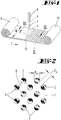
- the Figure 1 shows, roughly schematically, a variant of the method in which a substrate 1 coated with a metal layer 2 is wound onto a first reel 9 from which it is unwound in a transport direction T.
- a laser beam 4 is generated with a point-shaped cross-section.
- the punctiform laser beam 4 is expanded into a linear laser beam 5 with an optical expansion device 7.
- the width of the linear laser beam 5 corresponds at least to the width W of the substrate 1 in the area of its impingement on the layer 2.
- the widened laser beam 5 creates a linear exposure zone 15 on the surface of the substrate coated with a layer 2.
- the exposure zone 15 becomes the same at every point Time energy is coupled into the metal layer 2 in the form of heat. Because of the simultaneous exposure of the entire linear surface, there is virtually no temperature gradient in the direction of the line extension, but only in the direction of movement of the exposure zone 15.
- the island-shaped seed zones 3 lie approximately on the corner points of squares and have a diameter of R Dot from 1 to 100 nm.
- the individual island-shaped seed zones 3 are spaced from one another by the distance D Dc from 1 to 100 nm.
- the transport speed is about 5 to 30 cm / s.
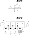
- the Figure 4 shows roughly schematically the structure of a device for depositing carbon nanotubes 16 on a substrate 1.
- the substrate 1 consisting of a metal, for example copper or aluminum, is unwound from a first winding 1 and at a transport speed through a production device consisting of several stages transported through.
- the treated substrate is rewound on a second reel 10.
- the device has a first station 11 at which a metal layer 2 is deposited on the substrate 1.
- a second station 12 then takes place with a device according to Figure 1 is formed, a surface treatment of the metal layer 2 with an expanded laser beam, so that the spaced-apart point-shaped seed zones 3 are formed.
- carbon nanotubes 16 are then deposited on the seed zones 3.
- further treatment steps can then be carried out, which are usually are required to manufacture electrodes for a lithium-ion battery.
- the island-shaped seed zones 3 are shown greatly enlarged in order to illustrate their uniform arrangement on the substrate 1. In reality, the islands 3 are spaced apart from one another in the submicron range.
- the area of the island-shaped seed zones 3 and the distance between the island-shaped seed zones 3 can be set in a reproducible manner using the parameters given above, such as laser power and layer thickness.
- a closed metal layer is first deposited on an unstructured substrate.
- the metal layer preferably completely covers the substrate surface, so that the width of the metal layer corresponds to the width of the substrate.
- An expanded laser beam the width of which corresponds to the width of the metal layer, is used to simultaneously energize the metal layer over its entire width.
- the substrate is transported relative to the linear laser treatment zone, so that the laser treatment zone moves over the substrate.
- the invention thus preferably relates to a method for producing a structured seed layer for depositing carbon nanotubes thereon 16, whereby a closed homogeneous metal layer 2 is first applied to an unstructured surface of a substrate 1 and then the metal layer 2 is energized with a laser beam 4, the laser beam 4 being expanded to form a beam 5 with a linear cross-section, with which a line-shaped beam is at the same time Exposure zone 15 of the metal layer 2 is exposed, the exposure zone 15 migrating over the metal layer 2 with such a migration speed in a direction transverse to its direction of extension and the laser beam 4 in the exposure zone 15 energizing the metal layer with such an energy density that the metal layer 2 closes isolated islands 3 of essentially the same size, which are essentially equally spaced from one another, the circle-equivalent diameter of the islands 3 being less than 2 ⁇ m and the distance between two adjacent islands 3 free of metal layers being less than Is 2 ⁇ m.
- the extent of the laser beam 5 measured in the direction of travel is preferably in a range between 0.5 mm and 1.5 mm.
- the pulse sequence is so high that the exposure zone 15 is literally continuously exposed to light.
- the pulse frequency is in particular much greater (factor 10) than the quotient of the migration speed and the width of the exposure zone 15. While no temperature gradient is established in the metal layer 2 melted by the laser exposure over the length of the exposure zone 15, i.e. in the line direction of the expanded laser beam a high temperature gradient in the direction of travel of the laser beam.
- Substrate 2 Metal layer 3 Islands 4th laser beam 5 expanded laser beam 6th laser T Transport direction 7th optics W. Expanse 8th Unit cell 9 Wrap 10 Wrap 11 first stop 12th second station 13th another station 14th 15th Exposure zone 16 Carbon nanotubes
Landscapes
- Engineering & Computer Science (AREA)
- Physics & Mathematics (AREA)
- Optics & Photonics (AREA)
- Chemical & Material Sciences (AREA)
- Plasma & Fusion (AREA)
- Mechanical Engineering (AREA)
- Materials Engineering (AREA)
- Organic Chemistry (AREA)
- Nanotechnology (AREA)
- Chemical Kinetics & Catalysis (AREA)
- Inorganic Chemistry (AREA)
- Condensed Matter Physics & Semiconductors (AREA)
- General Physics & Mathematics (AREA)
- Manufacturing & Machinery (AREA)
- Crystallography & Structural Chemistry (AREA)
- Laser Beam Processing (AREA)
- Carbon And Carbon Compounds (AREA)
- Optical Fibers, Optical Fiber Cores, And Optical Fiber Bundles (AREA)
Claims (14)
- Procédé de fabrication d'une couche de germination structurée pour le dépôt sur celle-ci de nanotubes de carbone (16), dans lequel une couche métallique (2) appliquée auparavant sur un substrat (1) est soumise à de l'énergie avec un faisceau laser (4) de manière que la couche métallique (2) se modifie, caractérisé en ce que des îlots individuels (3) sont produits en élargissant le faisceau laser (4) en un faisceau linéaire (5) en section transversale et en irradiant simultanément une zone d'irradiation linéaire (15) de la couche métallique (2), qui se déplace dans une direction transversale à sa direction d'extension sur la couche métallique (2).
- Procédé selon la revendication 1, caractérisé en ce que la largeur (W) du faisceau laser correspond à une largeur du substrat (1) et se situe dans une plage comprise entre 20 mm et 1000 mm ou entre 100 mm et 1000 mm.
- Procédé selon la revendication 2, caractérisé en ce que la largeur (W) du faisceau laser élargi (5) est comprise entre 300 et 600 mm.
- Procédé selon l'une des revendications précédentes, caractérisé en ce que le substrat (1) est constitué de silicium, de saphir, d'aluminium, de cuivre ou d'un autre métal.
- Procédé selon l'une des revendications précédentes, caractérisé en ce que la couche métallique (2) est constituée d'aluminium, de nickel, d'argent, d'or, de lithium, de titane, de vanadium, de chrome, de fer, de platine, de tantale ou d'un autre métal précieux ou non précieux.
- Procédé selon l'une des revendications précédentes, caractérisé en ce que l'épaisseur de la couche métallique est comprise entre 1 et 200 nm.
- Procédé selon l'une des revendications précédentes, caractérisé en ce que la longueur du faisceau laser s'étendant transversalement à la largeur (W) du faisceau laser élargi (5) et correspondant à la largeur de la zone d'irradiation (15) est de 0,5 à 5 mm.
- Procédé selon l'une des revendications précédentes, caractérisé en ce que la longueur d'onde de la lumière générée par le laser (6) est comprise entre 200 nm et 1,5 µm.
- Procédé selon l'une des revendications précédentes, caractérisé en ce que le laser (6) émet une lumière pulsée ou continue, l'énergie des impulsions étant comprise entre 0,5 et 20 mJ.
- Procédé selon l'une des revendications précédentes, caractérisé en ce que la vitesse à laquelle le faisceau laser élargi (5) se déplace sur la couche métallique (2) est comprise entre 1 et 50 cm/s, de préférence entre 5 et 30 cm/s.
- Procédé selon l'une des revendications précédentes, caractérisé en ce que les zones de germination en forme d'îlots (3) ont des diamètres circulaires équivalents de 1 nm à 2 µm, de préférence de 1 nm à 500 nm, de manière particulièrement préférée de 1 nm à 100 nm, et/ou en ce que les distances entre les centres des zones de germination en forme d'îlots (3) adjacentes sont dans la plage entre 1 nm et 2 µm, de préférence entre 1 nm et 500 nm, de manière particulièrement préférée entre 1 et 100 nm.
- Procédé selon l'une des revendications précédentes, caractérisé par un agencement rectangulaire, en particulier carré ou presque carré, des zones de germination (3) en forme d'îlots.
- Dispositif pour la mise en œuvre du procédé selon l'une des revendications précédentes, comprenant un laser (6) pour générer un faisceau laser, caractérisé par les caractéristiques suivantes :
un dispositif (9, 10) pour le transport d'un substrat (1) sur lequel est appliqué une couche métallique (2), un dispositif (7) pour l'élargissement du faisceau laser pour produire une zone d'irradiation linéaire (15), le dispositif (7) étant disposé de manière que la zone d'irradiation linéaire (15) s'étende perpendiculairement à la direction de transport du substrat (1), un dispositif pour dérouler un substrat enroulé sur une bobine (9), un dispositif (13) pour déposer des nanotubes de carbone (16) sur les zones de germination en forme d'îlots (3) et un dispositif pour supporter une bobine (10) sur laquelle le substrat traité est enroulé. - Dispositif selon la revendication 13, caractérisé par un dispositif (11) pour revêtir le substrat (1) d'une couche métallique (2), qui est agencé dans une direction de transport du substrat (1) en amont du dispositif (7) pour élargir le faisceau laser.
Applications Claiming Priority (2)
| Application Number | Priority Date | Filing Date | Title |
|---|---|---|---|
| DE102016121462.0A DE102016121462A1 (de) | 2016-11-09 | 2016-11-09 | Strukturierte Keimschicht |
| PCT/EP2017/078545 WO2018087118A1 (fr) | 2016-11-09 | 2017-11-08 | Procédé de production d'une couche de germination structurée au moyen d'un faisceau laser, dispositif correspondant |
Publications (2)
| Publication Number | Publication Date |
|---|---|
| EP3538314A1 EP3538314A1 (fr) | 2019-09-18 |
| EP3538314B1 true EP3538314B1 (fr) | 2021-10-20 |
Family
ID=60574522
Family Applications (1)
| Application Number | Title | Priority Date | Filing Date |
|---|---|---|---|
| EP17808782.1A Active EP3538314B1 (fr) | 2016-11-09 | 2017-11-08 | Procédé de production d'une couche de germination structurée au moyen d'un faisceau laser, dispositif correspondant |
Country Status (8)
| Country | Link |
|---|---|
| US (1) | US11052486B2 (fr) |
| EP (1) | EP3538314B1 (fr) |
| JP (1) | JP7075938B2 (fr) |
| KR (1) | KR102470077B1 (fr) |
| CN (1) | CN110087816B (fr) |
| DE (1) | DE102016121462A1 (fr) |
| TW (1) | TWI791469B (fr) |
| WO (1) | WO2018087118A1 (fr) |
Families Citing this family (3)
| Publication number | Priority date | Publication date | Assignee | Title |
|---|---|---|---|---|
| DE102019216070A1 (de) * | 2019-10-18 | 2021-04-22 | Trumpf Laser- Und Systemtechnik Gmbh | Verfahren zum Bearbeiten einer Lithiumfolie oder einer mit Lithium beschichteten Metallfolie mittels eines Laserstrahls |
| KR102774712B1 (ko) * | 2022-06-02 | 2025-03-04 | 재단법인대구경북과학기술원 | 레이저 공정으로 형성된 나노-섬 구조체를 포함하는 전자 소자 및 이의 제조 방법 |
| CN119658143B (zh) * | 2025-01-15 | 2025-09-23 | 华中科技大学 | 一种基于纳秒激光的金属表面微结构精准化制备方法及装置 |
Family Cites Families (25)
| Publication number | Priority date | Publication date | Assignee | Title |
|---|---|---|---|---|
| US5366140A (en) * | 1993-09-30 | 1994-11-22 | Minnesota Mining And Manufacturing Company | Patterned array of uniform metal microbeads |
| ATE192692T1 (de) * | 1999-01-28 | 2000-05-15 | Leister Process Tech | Laserfügeverfahren und vorrichtung zum verbinden von verschiedenen werkstücken aus kunststoff oder kunststoff mit anderen materialien |
| US7335908B2 (en) * | 2002-07-08 | 2008-02-26 | Qunano Ab | Nanostructures and methods for manufacturing the same |
| JP4494045B2 (ja) | 2003-03-11 | 2010-06-30 | 株式会社半導体エネルギー研究所 | ビームホモジナイザ及びレーザ照射装置、並びに半導体装置の作製方法 |
| KR100560244B1 (ko) * | 2003-06-13 | 2006-03-10 | 삼성코닝 주식회사 | 탄소나노구조체 또는 나노와이어를 이용한 전계 방출어레이 및 그 제조 방법 |
| TWI372463B (en) * | 2003-12-02 | 2012-09-11 | Semiconductor Energy Lab | Laser irradiation apparatus, laser irradiation method, and method for manufacturing semiconductor device |
| US20050237895A1 (en) * | 2004-04-23 | 2005-10-27 | Semiconductor Energy Laboratory Co., Ltd. | Laser irradiation apparatus and method for manufacturing semiconductor device |
| CN101111925A (zh) * | 2004-11-18 | 2008-01-23 | 纽约市哥伦比亚大学理事会 | 用于产生结晶方向受控的多晶硅膜的系统和方法 |
| JP4515473B2 (ja) | 2007-02-15 | 2010-07-28 | 株式会社半導体エネルギー研究所 | 半導体装置の作製方法 |
| JP4915309B2 (ja) | 2007-08-02 | 2012-04-11 | Jfeエンジニアリング株式会社 | 電子放出素子とその作製方法及びそれを装着した装置 |
| TWI359205B (en) * | 2007-09-21 | 2012-03-01 | Hon Hai Prec Ind Co Ltd | Growth equipment of carbon nanotube |
| KR20090041765A (ko) * | 2007-10-24 | 2009-04-29 | 삼성모바일디스플레이주식회사 | 탄소나노튜브 및 그 형성 방법, 하이브리드 구조 및 그형성 방법 및 발광 디바이스 |
| WO2010032965A2 (fr) * | 2008-09-17 | 2010-03-25 | 한국화학연구원 | Procédé de dépôt de matériau nanoporeux pour régulation du transfert thermique, dépôt de couche au moyen de ce procédé, substrat comprenant une telle couche, élément régulateur thermique et système correspondant |
| KR101097888B1 (ko) * | 2009-11-16 | 2011-12-23 | 전북대학교산학협력단 | 질화물계 반도체 발광 소자 및 기판 제조 방법 |
| DE102009059193B4 (de) * | 2009-12-17 | 2024-02-15 | Innolas Solutions Gmbh | Verfahren zur Dotierung von Halbleitermaterialien |
| JP2011174097A (ja) | 2010-02-23 | 2011-09-08 | Hitachi Zosen Corp | 熱cvd法および熱cvd装置並びにカーボンナノチューブの製造方法および製造装置 |
| JP2012045672A (ja) * | 2010-08-27 | 2012-03-08 | Hitachi Ltd | レーザー誘起表面層を有する3次元構造体及びその製造方法 |
| DE102011011734B4 (de) * | 2011-02-10 | 2014-12-24 | Fraunhofer-Gesellschaft zur Förderung der angewandten Forschung e.V. | Vorrichtung, Anordnung und Verfahren zur Interferenzstrukturierung von flächigen Proben |
| EP2591875B1 (fr) * | 2011-11-09 | 2017-01-25 | Leister Technologies AG | Laser doté d'une lentille de transformation du rayonnement |
| JP2014084245A (ja) | 2012-10-23 | 2014-05-12 | Hitachi Zosen Corp | カーボンナノチューブの切断方法および切断装置 |
| WO2014192955A1 (fr) | 2013-05-29 | 2014-12-04 | 東京エレクトロン株式会社 | Procédé permettant de produire du graphène et procéder permettant de faire croître des nanotubes de carbone |
| JP2014237557A (ja) * | 2013-06-06 | 2014-12-18 | 東京エレクトロン株式会社 | カーボンナノチューブ成長方法 |
| FR3009833B1 (fr) * | 2013-08-20 | 2015-10-16 | Saint Gobain | Procede d'obtention d'un substrat muni d'un revetement comprenant une couche mince metallique discontinue |
| EP3044178A1 (fr) | 2013-09-10 | 2016-07-20 | Saint-Gobain Glass France | Procédé laser pour la mise en uvre de nanoparticules métalliques à l'intérieur de la surface de substrats en verre de grande taille |
| KR20150035211A (ko) * | 2013-09-27 | 2015-04-06 | 서울바이오시스 주식회사 | 넓은 지향각 및 균일한 조도를 갖는 발광 소자 및 그 제조 방법 |
-
2016
- 2016-11-09 DE DE102016121462.0A patent/DE102016121462A1/de not_active Withdrawn
-
2017
- 2017-11-08 WO PCT/EP2017/078545 patent/WO2018087118A1/fr not_active Ceased
- 2017-11-08 EP EP17808782.1A patent/EP3538314B1/fr active Active
- 2017-11-08 US US16/346,975 patent/US11052486B2/en active Active
- 2017-11-08 JP JP2019546067A patent/JP7075938B2/ja active Active
- 2017-11-08 KR KR1020197014592A patent/KR102470077B1/ko active Active
- 2017-11-08 CN CN201780078259.XA patent/CN110087816B/zh active Active
- 2017-11-09 TW TW106138794A patent/TWI791469B/zh active
Non-Patent Citations (1)
| Title |
|---|
| None * |
Also Published As
| Publication number | Publication date |
|---|---|
| JP7075938B2 (ja) | 2022-05-26 |
| JP2019535534A (ja) | 2019-12-12 |
| US11052486B2 (en) | 2021-07-06 |
| CN110087816B (zh) | 2021-12-21 |
| WO2018087118A1 (fr) | 2018-05-17 |
| TW201822929A (zh) | 2018-07-01 |
| US20200061749A1 (en) | 2020-02-27 |
| KR20190084263A (ko) | 2019-07-16 |
| TWI791469B (zh) | 2023-02-11 |
| KR102470077B1 (ko) | 2022-11-23 |
| CN110087816A (zh) | 2019-08-02 |
| DE102016121462A1 (de) | 2018-05-09 |
| EP3538314A1 (fr) | 2019-09-18 |
Similar Documents
| Publication | Publication Date | Title |
|---|---|---|
| DE69220151T2 (de) | Verfahren und gerät zur erzeugung von kontakten | |
| DE69515020T2 (de) | Verfahren zum Züchten eines Halbleiterkristalls | |
| DE102004038339B4 (de) | Waferbearbeitungsverfahren | |
| EP3592696B1 (fr) | Procédé et dispositif de mise à disposition d'une pluralité de nanofils | |
| EP1733418A1 (fr) | Procede de traitement de surfaces de substrats | |
| EP3538314B1 (fr) | Procédé de production d'une couche de germination structurée au moyen d'un faisceau laser, dispositif correspondant | |
| WO2015090284A1 (fr) | Procédé de fabrication de particules abrasives multicouches | |
| DE3815006A1 (de) | Vorrichtung zum herstellen von beschichtungen mit abgestufter zusammensetzung | |
| DE2933850A1 (de) | Plasma-aetzvorrichtung | |
| EP2774184B1 (fr) | Procédé et dispositif pour réaliser une mise en contact électroconductrice, assistée par laser, d'une surface d'objet | |
| DE102015212444B4 (de) | Verfahren zur Herstellung einer Blechplatine | |
| DE10215999A1 (de) | Verfahren zur Herstellung von faserverstärktem Halbzeug in Form von Metallbändern, Metallblechen oder dergleichen sowie Vorrichtung zur Durchführung des Verfahrens | |
| DE2217086A1 (de) | Metallischer Verbundstreifen | |
| EP4118048A1 (fr) | Procédé de mise en forme d'un substrat support pour un élément optique fonctionnel | |
| DE102017000528A1 (de) | Verfahren zur Bearbeitung einer Halteplatte, insbesondere für einen Clamp zur Waferhalterung | |
| DE102008048342B4 (de) | SERS-Substrat, Verfahren zu seiner Herstellung und Verfahren zum Detektieren eines Analyten mittels SERS | |
| DE19946182A1 (de) | Verfahren und Anordnung zur Herstellung von Kohlstoff Nanoröhren | |
| DE102019205289B4 (de) | Anlage zur Herstellung elektrischer Kontaktelemente mit selektiv veredelten elektrischen Kontaktflächen | |
| DE2526382C3 (de) | Kathodenzerstäubungsverf ahren zur Herstellung geätzter Strukturen | |
| WO2017202579A1 (fr) | Élément optique et système de lithographique extrême ultraviolet | |
| DE102013000407B4 (de) | Verfahren zur Verbesserung der Benetzbarkeit einer rotierenden Elektrode in einer Gasentladungslampe | |
| DE102023209145B4 (de) | Bearbeitungsverfahren eines substrats und herstellungsverfahren für chips | |
| EP2206153B1 (fr) | Procédé de production de nanostructures par démouillage spinodal | |
| DE102015100885A1 (de) | Verfahren und Vorrichtung zur Behandlung eines beschichteten Substrats | |
| EP3812161B1 (fr) | Procédé et dispositif de revêtement d'un substrat, découpe et emballage |
Legal Events
| Date | Code | Title | Description |
|---|---|---|---|
| STAA | Information on the status of an ep patent application or granted ep patent |
Free format text: STATUS: UNKNOWN |
|
| STAA | Information on the status of an ep patent application or granted ep patent |
Free format text: STATUS: THE INTERNATIONAL PUBLICATION HAS BEEN MADE |
|
| PUAI | Public reference made under article 153(3) epc to a published international application that has entered the european phase |
Free format text: ORIGINAL CODE: 0009012 |
|
| STAA | Information on the status of an ep patent application or granted ep patent |
Free format text: STATUS: REQUEST FOR EXAMINATION WAS MADE |
|
| 17P | Request for examination filed |
Effective date: 20190523 |
|
| AK | Designated contracting states |
Kind code of ref document: A1 Designated state(s): AL AT BE BG CH CY CZ DE DK EE ES FI FR GB GR HR HU IE IS IT LI LT LU LV MC MK MT NL NO PL PT RO RS SE SI SK SM TR |
|
| AX | Request for extension of the european patent |
Extension state: BA ME |
|
| DAV | Request for validation of the european patent (deleted) | ||
| DAX | Request for extension of the european patent (deleted) | ||
| STAA | Information on the status of an ep patent application or granted ep patent |
Free format text: STATUS: EXAMINATION IS IN PROGRESS |
|
| 17Q | First examination report despatched |
Effective date: 20200907 |
|
| GRAP | Despatch of communication of intention to grant a patent |
Free format text: ORIGINAL CODE: EPIDOSNIGR1 |
|
| STAA | Information on the status of an ep patent application or granted ep patent |
Free format text: STATUS: GRANT OF PATENT IS INTENDED |
|
| INTG | Intention to grant announced |
Effective date: 20210520 |
|
| GRAS | Grant fee paid |
Free format text: ORIGINAL CODE: EPIDOSNIGR3 |
|
| GRAA | (expected) grant |
Free format text: ORIGINAL CODE: 0009210 |
|
| STAA | Information on the status of an ep patent application or granted ep patent |
Free format text: STATUS: THE PATENT HAS BEEN GRANTED |
|
| AK | Designated contracting states |
Kind code of ref document: B1 Designated state(s): AL AT BE BG CH CY CZ DE DK EE ES FI FR GB GR HR HU IE IS IT LI LT LU LV MC MK MT NL NO PL PT RO RS SE SI SK SM TR |
|
| REG | Reference to a national code |
Ref country code: GB Ref legal event code: FG4D Free format text: NOT ENGLISH |
|
| REG | Reference to a national code |
Ref country code: CH Ref legal event code: EP |
|
| REG | Reference to a national code |
Ref country code: IE Ref legal event code: FG4D Free format text: LANGUAGE OF EP DOCUMENT: GERMAN |
|
| REG | Reference to a national code |
Ref country code: DE Ref legal event code: R096 Ref document number: 502017011794 Country of ref document: DE |
|
| REG | Reference to a national code |
Ref country code: AT Ref legal event code: REF Ref document number: 1439521 Country of ref document: AT Kind code of ref document: T Effective date: 20211115 |
|
| REG | Reference to a national code |
Ref country code: LT Ref legal event code: MG9D |
|
| REG | Reference to a national code |
Ref country code: NL Ref legal event code: MP Effective date: 20211020 |
|
| PG25 | Lapsed in a contracting state [announced via postgrant information from national office to epo] |
Ref country code: RS Free format text: LAPSE BECAUSE OF FAILURE TO SUBMIT A TRANSLATION OF THE DESCRIPTION OR TO PAY THE FEE WITHIN THE PRESCRIBED TIME-LIMIT Effective date: 20211020 Ref country code: LT Free format text: LAPSE BECAUSE OF FAILURE TO SUBMIT A TRANSLATION OF THE DESCRIPTION OR TO PAY THE FEE WITHIN THE PRESCRIBED TIME-LIMIT Effective date: 20211020 Ref country code: FI Free format text: LAPSE BECAUSE OF FAILURE TO SUBMIT A TRANSLATION OF THE DESCRIPTION OR TO PAY THE FEE WITHIN THE PRESCRIBED TIME-LIMIT Effective date: 20211020 Ref country code: BG Free format text: LAPSE BECAUSE OF FAILURE TO SUBMIT A TRANSLATION OF THE DESCRIPTION OR TO PAY THE FEE WITHIN THE PRESCRIBED TIME-LIMIT Effective date: 20220120 |
|
| PG25 | Lapsed in a contracting state [announced via postgrant information from national office to epo] |
Ref country code: IS Free format text: LAPSE BECAUSE OF FAILURE TO SUBMIT A TRANSLATION OF THE DESCRIPTION OR TO PAY THE FEE WITHIN THE PRESCRIBED TIME-LIMIT Effective date: 20220220 Ref country code: SE Free format text: LAPSE BECAUSE OF FAILURE TO SUBMIT A TRANSLATION OF THE DESCRIPTION OR TO PAY THE FEE WITHIN THE PRESCRIBED TIME-LIMIT Effective date: 20211020 Ref country code: PT Free format text: LAPSE BECAUSE OF FAILURE TO SUBMIT A TRANSLATION OF THE DESCRIPTION OR TO PAY THE FEE WITHIN THE PRESCRIBED TIME-LIMIT Effective date: 20220221 Ref country code: PL Free format text: LAPSE BECAUSE OF FAILURE TO SUBMIT A TRANSLATION OF THE DESCRIPTION OR TO PAY THE FEE WITHIN THE PRESCRIBED TIME-LIMIT Effective date: 20211020 Ref country code: NO Free format text: LAPSE BECAUSE OF FAILURE TO SUBMIT A TRANSLATION OF THE DESCRIPTION OR TO PAY THE FEE WITHIN THE PRESCRIBED TIME-LIMIT Effective date: 20220120 Ref country code: NL Free format text: LAPSE BECAUSE OF FAILURE TO SUBMIT A TRANSLATION OF THE DESCRIPTION OR TO PAY THE FEE WITHIN THE PRESCRIBED TIME-LIMIT Effective date: 20211020 Ref country code: LV Free format text: LAPSE BECAUSE OF FAILURE TO SUBMIT A TRANSLATION OF THE DESCRIPTION OR TO PAY THE FEE WITHIN THE PRESCRIBED TIME-LIMIT Effective date: 20211020 Ref country code: HR Free format text: LAPSE BECAUSE OF FAILURE TO SUBMIT A TRANSLATION OF THE DESCRIPTION OR TO PAY THE FEE WITHIN THE PRESCRIBED TIME-LIMIT Effective date: 20211020 Ref country code: GR Free format text: LAPSE BECAUSE OF FAILURE TO SUBMIT A TRANSLATION OF THE DESCRIPTION OR TO PAY THE FEE WITHIN THE PRESCRIBED TIME-LIMIT Effective date: 20220121 Ref country code: ES Free format text: LAPSE BECAUSE OF FAILURE TO SUBMIT A TRANSLATION OF THE DESCRIPTION OR TO PAY THE FEE WITHIN THE PRESCRIBED TIME-LIMIT Effective date: 20211020 |
|
| REG | Reference to a national code |
Ref country code: CH Ref legal event code: PL |
|
| REG | Reference to a national code |
Ref country code: DE Ref legal event code: R097 Ref document number: 502017011794 Country of ref document: DE |
|
| PG25 | Lapsed in a contracting state [announced via postgrant information from national office to epo] |
Ref country code: SM Free format text: LAPSE BECAUSE OF FAILURE TO SUBMIT A TRANSLATION OF THE DESCRIPTION OR TO PAY THE FEE WITHIN THE PRESCRIBED TIME-LIMIT Effective date: 20211020 Ref country code: SK Free format text: LAPSE BECAUSE OF FAILURE TO SUBMIT A TRANSLATION OF THE DESCRIPTION OR TO PAY THE FEE WITHIN THE PRESCRIBED TIME-LIMIT Effective date: 20211020 Ref country code: RO Free format text: LAPSE BECAUSE OF FAILURE TO SUBMIT A TRANSLATION OF THE DESCRIPTION OR TO PAY THE FEE WITHIN THE PRESCRIBED TIME-LIMIT Effective date: 20211020 Ref country code: MC Free format text: LAPSE BECAUSE OF FAILURE TO SUBMIT A TRANSLATION OF THE DESCRIPTION OR TO PAY THE FEE WITHIN THE PRESCRIBED TIME-LIMIT Effective date: 20211020 Ref country code: LU Free format text: LAPSE BECAUSE OF NON-PAYMENT OF DUE FEES Effective date: 20211108 Ref country code: EE Free format text: LAPSE BECAUSE OF FAILURE TO SUBMIT A TRANSLATION OF THE DESCRIPTION OR TO PAY THE FEE WITHIN THE PRESCRIBED TIME-LIMIT Effective date: 20211020 Ref country code: DK Free format text: LAPSE BECAUSE OF FAILURE TO SUBMIT A TRANSLATION OF THE DESCRIPTION OR TO PAY THE FEE WITHIN THE PRESCRIBED TIME-LIMIT Effective date: 20211020 Ref country code: CZ Free format text: LAPSE BECAUSE OF FAILURE TO SUBMIT A TRANSLATION OF THE DESCRIPTION OR TO PAY THE FEE WITHIN THE PRESCRIBED TIME-LIMIT Effective date: 20211020 Ref country code: BE Free format text: LAPSE BECAUSE OF NON-PAYMENT OF DUE FEES Effective date: 20211130 |
|
| REG | Reference to a national code |
Ref country code: BE Ref legal event code: MM Effective date: 20211130 |
|
| PLBE | No opposition filed within time limit |
Free format text: ORIGINAL CODE: 0009261 |
|
| STAA | Information on the status of an ep patent application or granted ep patent |
Free format text: STATUS: NO OPPOSITION FILED WITHIN TIME LIMIT |
|
| 26N | No opposition filed |
Effective date: 20220721 |
|
| PG25 | Lapsed in a contracting state [announced via postgrant information from national office to epo] |
Ref country code: IE Free format text: LAPSE BECAUSE OF NON-PAYMENT OF DUE FEES Effective date: 20211108 Ref country code: AL Free format text: LAPSE BECAUSE OF FAILURE TO SUBMIT A TRANSLATION OF THE DESCRIPTION OR TO PAY THE FEE WITHIN THE PRESCRIBED TIME-LIMIT Effective date: 20211020 |
|
| PG25 | Lapsed in a contracting state [announced via postgrant information from national office to epo] |
Ref country code: SI Free format text: LAPSE BECAUSE OF FAILURE TO SUBMIT A TRANSLATION OF THE DESCRIPTION OR TO PAY THE FEE WITHIN THE PRESCRIBED TIME-LIMIT Effective date: 20211020 |
|
| PG25 | Lapsed in a contracting state [announced via postgrant information from national office to epo] |
Ref country code: IT Free format text: LAPSE BECAUSE OF FAILURE TO SUBMIT A TRANSLATION OF THE DESCRIPTION OR TO PAY THE FEE WITHIN THE PRESCRIBED TIME-LIMIT Effective date: 20211020 |
|
| PG25 | Lapsed in a contracting state [announced via postgrant information from national office to epo] |
Ref country code: CY Free format text: LAPSE BECAUSE OF FAILURE TO SUBMIT A TRANSLATION OF THE DESCRIPTION OR TO PAY THE FEE WITHIN THE PRESCRIBED TIME-LIMIT Effective date: 20211020 |
|
| P01 | Opt-out of the competence of the unified patent court (upc) registered |
Effective date: 20230528 |
|
| PG25 | Lapsed in a contracting state [announced via postgrant information from national office to epo] |
Ref country code: LI Free format text: LAPSE BECAUSE OF NON-PAYMENT OF DUE FEES Effective date: 20220630 Ref country code: HU Free format text: LAPSE BECAUSE OF FAILURE TO SUBMIT A TRANSLATION OF THE DESCRIPTION OR TO PAY THE FEE WITHIN THE PRESCRIBED TIME-LIMIT; INVALID AB INITIO Effective date: 20171108 Ref country code: CH Free format text: LAPSE BECAUSE OF NON-PAYMENT OF DUE FEES Effective date: 20220630 |
|
| REG | Reference to a national code |
Ref country code: AT Ref legal event code: MM01 Ref document number: 1439521 Country of ref document: AT Kind code of ref document: T Effective date: 20221108 |
|
| PG25 | Lapsed in a contracting state [announced via postgrant information from national office to epo] |
Ref country code: AT Free format text: LAPSE BECAUSE OF NON-PAYMENT OF DUE FEES Effective date: 20221108 |
|
| PG25 | Lapsed in a contracting state [announced via postgrant information from national office to epo] |
Ref country code: MK Free format text: LAPSE BECAUSE OF FAILURE TO SUBMIT A TRANSLATION OF THE DESCRIPTION OR TO PAY THE FEE WITHIN THE PRESCRIBED TIME-LIMIT Effective date: 20211020 |
|
| PG25 | Lapsed in a contracting state [announced via postgrant information from national office to epo] |
Ref country code: MT Free format text: LAPSE BECAUSE OF FAILURE TO SUBMIT A TRANSLATION OF THE DESCRIPTION OR TO PAY THE FEE WITHIN THE PRESCRIBED TIME-LIMIT Effective date: 20211020 |
|
| PGFP | Annual fee paid to national office [announced via postgrant information from national office to epo] |
Ref country code: DE Payment date: 20250428 Year of fee payment: 8 |
|
| PGFP | Annual fee paid to national office [announced via postgrant information from national office to epo] |
Ref country code: GB Payment date: 20250428 Year of fee payment: 8 |
|
| PGFP | Annual fee paid to national office [announced via postgrant information from national office to epo] |
Ref country code: FR Payment date: 20250428 Year of fee payment: 8 |
|
| PG25 | Lapsed in a contracting state [announced via postgrant information from national office to epo] |
Ref country code: TR Free format text: LAPSE BECAUSE OF FAILURE TO SUBMIT A TRANSLATION OF THE DESCRIPTION OR TO PAY THE FEE WITHIN THE PRESCRIBED TIME-LIMIT Effective date: 20211020 |