EP3540469B1 - Capteur d'images - Google Patents
Capteur d'images Download PDFInfo
- Publication number
- EP3540469B1 EP3540469B1 EP18161290.4A EP18161290A EP3540469B1 EP 3540469 B1 EP3540469 B1 EP 3540469B1 EP 18161290 A EP18161290 A EP 18161290A EP 3540469 B1 EP3540469 B1 EP 3540469B1
- Authority
- EP
- European Patent Office
- Prior art keywords
- dose
- pixels
- pixel
- stitching
- select
- Prior art date
- Legal status (The legal status is an assumption and is not a legal conclusion. Google has not performed a legal analysis and makes no representation as to the accuracy of the status listed.)
- Active
Links
Images



Classifications
-
- H—ELECTRICITY
- H10—SEMICONDUCTOR DEVICES; ELECTRIC SOLID-STATE DEVICES NOT OTHERWISE PROVIDED FOR
- H10F—INORGANIC SEMICONDUCTOR DEVICES SENSITIVE TO INFRARED RADIATION, LIGHT, ELECTROMAGNETIC RADIATION OF SHORTER WAVELENGTH OR CORPUSCULAR RADIATION
- H10F39/00—Integrated devices, or assemblies of multiple devices, comprising at least one element covered by group H10F30/00, e.g. radiation detectors comprising photodiode arrays
- H10F39/80—Constructional details of image sensors
- H10F39/802—Geometry or disposition of elements in pixels, e.g. address-lines or gate electrodes
- H10F39/8023—Disposition of the elements in pixels, e.g. smaller elements in the centre of the imager compared to larger elements at the periphery
-
- G—PHYSICS
- G01—MEASURING; TESTING
- G01T—MEASUREMENT OF NUCLEAR OR X-RADIATION
- G01T1/00—Measuring X-radiation, gamma radiation, corpuscular radiation, or cosmic radiation
- G01T1/16—Measuring radiation intensity
- G01T1/17—Circuit arrangements not adapted to a particular type of detector
-
- G—PHYSICS
- G01—MEASURING; TESTING
- G01T—MEASUREMENT OF NUCLEAR OR X-RADIATION
- G01T1/00—Measuring X-radiation, gamma radiation, corpuscular radiation, or cosmic radiation
- G01T1/16—Measuring radiation intensity
- G01T1/24—Measuring radiation intensity with semiconductor detectors
- G01T1/243—Modular detectors, e.g. arrays formed from self contained units
-
- H—ELECTRICITY
- H04—ELECTRIC COMMUNICATION TECHNIQUE
- H04N—PICTORIAL COMMUNICATION, e.g. TELEVISION
- H04N25/00—Circuitry of solid-state image sensors [SSIS]; Control thereof
- H04N25/30—Circuitry of solid-state image sensors [SSIS]; Control thereof for transforming X-rays into image signals
-
- H—ELECTRICITY
- H04—ELECTRIC COMMUNICATION TECHNIQUE
- H04N—PICTORIAL COMMUNICATION, e.g. TELEVISION
- H04N25/00—Circuitry of solid-state image sensors [SSIS]; Control thereof
- H04N25/70—SSIS architectures; Circuits associated therewith
- H04N25/76—Addressed sensors, e.g. MOS or CMOS sensors
- H04N25/77—Pixel circuitry, e.g. memories, A/D converters, pixel amplifiers, shared circuits or shared components
- H04N25/771—Pixel circuitry, e.g. memories, A/D converters, pixel amplifiers, shared circuits or shared components comprising storage means other than floating diffusion
-
- H—ELECTRICITY
- H04—ELECTRIC COMMUNICATION TECHNIQUE
- H04N—PICTORIAL COMMUNICATION, e.g. TELEVISION
- H04N25/00—Circuitry of solid-state image sensors [SSIS]; Control thereof
- H04N25/70—SSIS architectures; Circuits associated therewith
- H04N25/76—Addressed sensors, e.g. MOS or CMOS sensors
- H04N25/78—Readout circuits for addressed sensors, e.g. output amplifiers or A/D converters
-
- H—ELECTRICITY
- H10—SEMICONDUCTOR DEVICES; ELECTRIC SOLID-STATE DEVICES NOT OTHERWISE PROVIDED FOR
- H10F—INORGANIC SEMICONDUCTOR DEVICES SENSITIVE TO INFRARED RADIATION, LIGHT, ELECTROMAGNETIC RADIATION OF SHORTER WAVELENGTH OR CORPUSCULAR RADIATION
- H10F39/00—Integrated devices, or assemblies of multiple devices, comprising at least one element covered by group H10F30/00, e.g. radiation detectors comprising photodiode arrays
- H10F39/80—Constructional details of image sensors
- H10F39/803—Pixels having integrated switching, control, storage or amplification elements
Definitions
- the present invention relates to an image sensor. More in particular, the present invention relates to an image sensor that comprises dose sensing pixels to sense an incident dose of photons. Such dose sensing can be used to trigger an image capturing process. Such dose sensing is important in the field of X-ray imaging, where these image sensors can be used.
- a typical X-ray sensor configured for detecting X-rays comprises a matrix of rows and columns of photosensitive pixels.
- the matrix is covered with a scintillator layer that converts incoming X-ray photons into visible light photons that can be detected by the matrix of photosensitive pixels.
- an active matrix is used wherein pixels in a given row can be selected at the same time, and wherein the selected pixels can be read out at the same time using column-specific read-out circuitry.
- This read-out circuitry is configured for receiving a signal on a column line to which all pixels in the same column are connected. Accordingly, it is impossible to read out multiple selected pixels in the same column.
- the dose settings for the X-ray source need to be adjusted to the particular type of diagnosis, tissue type, etc.
- the emitted X-ray radiation needs to be utilized as efficiently as possible. In other words, the patient should not be exposed to X-ray radiation when this radiation is not used for imaging purposes.
- US 7659516B2 presents a solution to address this problem.
- This document discloses an image sensor in which some of the photosensitive pixels are designated as dose sensing pixels, hereinafter referred to as second pixels.
- these pixels are distributed over the entire matrix such that each column of the matrix comprises at most second pixel. This makes it possible to read out every second pixel at the same time as the distribution of the second pixels prevents the situation that second pixels in different rows but in the same column are simultaneously selected and read out.
- FIG 1 An image sensor 1 is shown that is manufactured using three reticle blocks 2, 3, 4 that are comprised in a reticle 5. As shown in figure 1 , the arrangement of reticle blocks 2, 3, 4 in reticle 5 may be different than in image sensor 1 itself. In such cases, image sensor 1 is formed by selectively using one of the reticle blocks 2, 3, 4 in a photolithography process while blocking the others. After each step, reticle 5 is re-aligned with the semiconductor substrate of image sensor 1 for a next lithography step using a different reticle block 2, 3, 4.
- the present invention does not exclude other arrangements of reticle blocks 2, 3, 4, for example wherein the reticle blocks 2, 3, 4 have an arrangement on reticle 5 that is similar or identical to the arrangement in image sensor 1.
- a single lithography step may be used per layer of image sensor 1.
- image sensor 1 is built up out of several layers, each layer being formed using a respective reticle 5.
- reference will be made to a single reticle 5 as opposed to a reticle set.
- reticle block 2 is used to define a matrix of pixels comprising a plurality of first pixels 6 and a plurality of second pixels 7.
- Reticle block 3 is used for defining a pixel select controller 8 that is configured for, in an image read-out mode of the image sensor, simultaneously selecting first pixels and second pixels in a given row, one row at a time.
- Pixel controller 8 is further configured for, in a dose sensing mode of the image sensor, simultaneously selecting second pixels in different rows.
- Image sensor 1 further comprises read-out circuitry 9 for reading out the photosensitive pixels.
- Read-out circuitry 9 comprises a plurality of column lines 10 that are each connected to a plurality of pixels 6, 7 that are arranged in the same column but in different rows.
- read-out circuitry 9 comprises a plurality of analog-to-digital converters (ADCs) 11 for converting the analog voltages into digital values and a collecting unit 12 for collecting and outputting the digital values. As shown in figure 1 , read-out circuitry 9 is formed using reticle block 4.
- ADCs analog-to-digital converters
- FIG. 2 presents an example of a known schematic for a pixel 20, referred to as a 3T layout, which can be used in the image sensor in figure 1 .
- pixel 20 may correspond to a first pixel 6 or a second pixel 7.
- Pixel 20 comprises a (pinned) photodiode 21, a primary storage capacitor 22, and a secondary storage capacitor 23 which can be switched using a switch 24.
- a scintillator layer (not illustrated) is applied over the pixel or is integrated therewith. This layer converts incoming X-rays into visible light which can be detected by photodiode 21.
- the operation of the pixel can be explained as follows.
- the voltage at the terminal between capacitor 22 and photodiode 21 is charged / reset to a predefined reference voltage Vref using a NMOST 25 in response to a reset signal received from pixel select controller 8.
- NMOST 25 is brought into in a non-conducting state.
- the voltage at this terminal is sensed using a source follower NMOST 26 that is connected to an NMOST 27 that acts as a selection FET.
- the voltage at the terminal of capacitor 22, referred to as the photo-voltage is fed through source follower 26 and selection FET 27 to read-out circuitry 9 via a pixel column line 10. There, the analog signal is converted into a digital value using ADC 11. As a final step, selection FET 27 is brought into a non-conductive state and the process is repeated.
- secondary storage capacitor 23 can be put parallel to primary storage capacitor 22. This allows the pixel to process a higher dose of X-rays as the effective storage capacitance has increased, and to thereby offer a different sensitivity.
- the skilled person will understand that having a secondary storage capacitor is optional.
- the invention equally relates to embodiments wherein storage capacitor 22 is intrinsically present in photodiode 21.
- first and second pixels 6, 7 are reset such that the photo-voltage is set to the predefined voltage Vref. Due to the generated photocurrent, the photo-voltage will decrease in dependence of the incoming X-ray dose. This photo-voltage cannot decrease indefinitely. A lower limit exists at which the photo-voltage is still a reliable measure for the incoming X-ray dose. If a higher dose has been used, the pixel will saturate and no information other than that the dose has exceeded a certain threshold can be derived from the reading.
- the integration time should be matched to the period during which the X-ray source emits X-ray radiation as closely as possible.
- US 7659516B2 proposes to use the information from second pixels 7 to set a starting point for the actual image capturing process. For example, if a dose is detected by second pixels 7 that exceeds a predefined threshold, the entire matrix is reset and the image capturing process starts. In this manner, only a limited amount of the X-ray dose is lost. More in particular, in the dose sensing mode, second pixels 7 are first reset to the predefined voltage. Thereafter, the photo-voltage of these pixels is monitored without resetting the photo-voltage, known as non-destructive read-out. When the measured dose, determined using the photo-voltage, exceeds a threshold, the operational mode of the image sensor is switched to the image read-out mode. Because the photo-voltage will gradually decrease due to dark currents, a false triggering may be generated. Therefore, the photo-voltage of second pixels 7 has to be reset regularly.
- the abovementioned solution is particularly applicable to relatively small sensors. For larger X-ray sensors, it can no longer be guaranteed that only a single second pixel is arranged for each column. This is related to the manner in which these sensors are constructed. More in particular, a wafer stepping technique is used in which the image sensor comprises a plurality of adjacently arranged identical stitching blocks. Each stitching block has been formed using wafer stepper lithography on the basis of the same reticle block(s). Therefore, if a second pixel is arranged for a given column in a given stitching block, and a further stitching block is adjacently arranged in the column direction, a total of two second pixels will be arranged for the same column. Therefore, the second pixels need to be addressed in a row specific manner during the dose sensing process, thereby resulting in a larger loss of X-ray dose that is not used for the actual image capturing.
- An object of the present invention is to provide a solution to this problem, allowing an efficient and fast dose sensing process in larger sensors that comprise a plurality of stitching blocks.
- each stitching block comprises a plurality of first pixels and a plurality of second pixels, a plurality of dose select lines configured for carrying respective dose select signals.
- Each stitching block further comprises a pixel select controller configured for, in an image read-out mode of the image sensor, simultaneously selecting first pixels and second pixels, in a given row and given stitching block, one row at a time.
- the pixel select controller is further configured for, in a dose sensing mode of the image sensor, simultaneously selecting second pixels in different rows and different stitching blocks in dependence of the dose select signals.
- the image sensor according to the invention further comprises, at each connecting interface between stitching blocks that are adjacently arranged in the column direction, a dose select line connecting unit for connecting each dose select line of a first stitching block among the adjacent stitching blocks to a respective dose select line of a second stitching block among the adjacent stitching blocks to prevent multiple second pixels in the same column of the matrix from being selected.
- second pixels in a stitching block are selected based on signal levels on the dose select lines.
- the dose select line connecting unit switches these signals at the interface between adjacent stitching blocks so that each stitching block displays a different distribution of the signals over the dose select lines.
- Each stitching block may comprise a first part arranged on a first side of the stitching block, and a second part arranged on a second side of the stitching block opposite to the first side, wherein the dose select line connecting unit at an interface between a pair of adjacently arranged stitching blocks comprises the first part of one stitching block among the adjacently arranged stitching blocks and the second part of the other stitching block among the adjacently arranged stitching blocks.
- each stitching block may comprise a respective dose select line connecting unit arranged on a first side of the stitching block.
- the dose select lines may be adjacently arranged in the row direction of the matrix in a given order, each dose select line having a given position within said order, wherein the position of a dose select line in a given stitching block is different from the position of the dose select line in the adjacently arranged stitching block to which it is connected.
- each stitching block among three stitching blocks that are adjacently arranged in the column direction may comprise 3 dose select lines extending in parallel to the column direction.
- the line arranged on the left is referred to as the first line (LI), the line in the middle as the second line (L2), and the line on the right as the third line (L3).
- the first line of the n th stitching block in the column direction, with n ranging from 1, corresponding to the stitching block on the top, to 3, corresponding to the stitching block on the bottom, is referred to as L1_n.
- L2_3 corresponds to the second line of the third stitching block.
- a possible embodiment of the invention is indicated in the table below: Dose select signal 1 Dose select signal 2 Dose select signal 3 L1_1 L2_1 L3_1 L2_2 L3_2 L1_2 L3_3 L1_3 L2_3
- a dose select signal 1 is put on L1_1. This line is electrically connected to L2_2 and L3_3 of the other stitching blocks. It can be verified that a given dose select signal is present on different lines in different stitching blocks.
- the pixel select controller may be configured for selecting the first pixels and the second pixels in the image read-out mode in dependence of a global select signal and a row-specific row select signal, and wherein the pixel select controller is configured for selecting the second pixels in the dose sensing mode in dependence of the global select signal and the dose select signals.
- the global select signal could be used to select every second pixel in the dose sensing mode.
- multiple stitching blocks are used. Using the dose select signals, the situation can be avoided wherein multiple second pixels are selected in the same column. In the image read-out mode, only a single row of pixels, including the first and second pixels, is selected at the same time. To that end, the selection of the first and second pixels can be made dependent on a row-specific row select signal.
- the image sensor may further comprise a row driver, preferably comprised in the pixel select controller, and configured for generating the row-specific row select signal for selecting pixels that are in the same row, and a timing generator for generating the global select signal, and at least one of the dose select signals.
- the row-specific row select signal may be generated by a shift register comprised in the pixel select controller.
- shift registers of stitching blocks that are adjacently arranged in the column direction are electrically coupled to each other to form one large shift register.
- a level of one or more of the dose select signals may be controllable between a low and a high level, and wherein the other dose select signals have a fixed level.
- the fixed level may correspond to a ground level, e.g. 0V.
- the dose select line(s) in each stitching block may be configured to provide a dose select signal for selecting a pattern of second pixels in that stitching block during the dose sensing mode, wherein the patterns of second pixels for different stitching blocks are different.
- the patterns of second pixels of different stitching blocks may be shifted in the row direction with respect to each other.
- each stitching block generally comprises the same connections required for the first and second pixels.
- a first pixel in a stitching block will generally only be used in the image read-out mode.
- a second pixel at a given position in a stitching block may, depending on the dose select signals during operation, only be used in the image read-out mode, whereas this same pixel but in a different stitching block may be used in the image read-out mode and in the dose sensing mode.
- the pixel select controller may comprise a plurality of identical pixel select sub-controller blocks that are adjacently arranged in the column direction and wherein each pixel select sub-controller block is configured, in the dose sensing mode, to select one among n second pixels that are arranged on respective and preferably adjacent rows, wherein n corresponds to the number of stitching blocks that are adjacently arranged in the column direction. Again, which second pixel is selected by a pixel select sub-controller block depends on the dose select signals.
- a pixel select sub-controller may be configured such that it is able to select one among three second pixels that are arranged in three adjacent rows. Moreover, these pixels are offset by one pixel in the row direction. The position of these pixels could for example be denoted as p, p+1, and p+2.
- this sub-controller arranged in the first stitching block, may select the second pixel at position p to be used in the dose sensing mode.
- This same sub-controller albeit arranged in the second stitching block, may select the second pixel at position p+1 to be used in the dose sensing mode. Selecting second pixels at different positions in different stitching blocks is made possible using the dose select line connecting unit.
- the number of stitching blocks adjacently arranged in the column direction is equal to the number of dose select lines.
- the image sensor may further comprise read-out circuitry for reading out photo-voltages of the photosensitive pixels.
- the read-out circuitry is connected to a plurality of column lines that each are arranged over each stitching block, each column line being connected to a plurality of pixels that are arranged in the same column but in different rows.
- the column lines are typically formed using line segments in the various stitching blocks that are mutually connected at the interfaces between the stitching blocks.
- the circuitry for reading the voltage on the column lines can be arranged on one end of image sensor and is typically formed using a different reticle block.
- Each of the first and second pixels may comprise a photodiode for generating a photocurrent, and a storage capacitor of which a terminal is connected to the photodiode, the voltage at the terminal being referred to as the photo-voltage.
- the pixel may further comprise a reset transistor for resetting the voltage at the terminal to a predefined voltage, a select transistor for selecting the pixel in dependence of a pixel select signal, and a source follower for feeding the photo-voltage to the column line to which the pixel is connected when the pixel is selected. This configuration is known as a 3T pixel.
- the image sensor may be configured to perform a correlated sampling scheme, wherein reading out a photo-voltage of a pixel in the image read-out mode may comprise a first read-out step in which the photo-voltage of the pixel is reset to a predefined value and is thereafter being allowed, during an integration time, to change in response to a dose of incident photons, the photo voltage being read as a first voltage after expiry of the integration time.
- the scheme may further comprise a second read-out step in which the photo-voltage of the pixel is reset to the predefined value and is directly subsequently read as a second voltage.
- the read-out circuitry may be configured to compute a pixel voltage by subtracting the first voltage from the second voltage.
- the image sensor may be configured to perform a correlated sampling scheme, wherein reading out a photo-voltage of a second pixel in the dose sensing mode comprises a step of re-setting the photo-voltage of the pixel to a predefined value, and a read-out step of reading the photo-voltage as a third voltage.
- the read-out circuitry may be configured to compute a pixel voltage by subtracting the third voltage from the predefined voltage. Whereas in the image read-out mode, the pixels are reset to a predefined voltage prior to each read-out, this does not apply for the second pixels in the dose sensing mode.
- the second pixels are read out in dependence of the dose select signals a multiple times before a next reset is performed. A reset may for instance be required if the photo-voltage has changed too much due to dark currents.
- the image sensor may be configured to switch or to be switched from the dose sensing mode to the image read-out mode when the dose determined in the dose sensing mode exceeds a predefined threshold.
- dose is generally determined by examining the pixel voltages of the dose sensing pixels.
- an average pixel voltage or dose may be determined for the entire collection of second pixels involved in the dose sensing mode.
- the invention does not exclude other thresholds to be used.
- the image sensor may be an X-ray sensor in which the matrix of pixels comprises a scintillator layer for converting an incoming X-ray photon into a visible light photon.
- the invention equally relates to optical sensors used in photography, etc.
- the invention provides an X-ray imaging system, comprising an X-ray source, an X-ray detector comprising the image sensor as defined above, and an image processing unit for constructing an X-ray image based on read-outs of the X-ray detector.
- image sensor 100 comprises a repetition or stitching of the various reticle blocks.
- the matrix of pixels comprises four identical stitching blocks, each corresponding to reticle block 102, and the pixel controller comprises two identical stitching blocks, each corresponding to reticle block 103.
- the pixel controller comprises a plurality of identical pixel select sub-controller blocks 108.
- Read-out circuitry 109 is formed using reticle block 104 and comprises the circuitry required for reading out each column of the matrix of pixels.
- a timing generator 113 may be formed using reticle block 104. It is noted that read-out circuitry 109 could also be formed using two stitching blocks that are stitched in the row direction. In such embodiment, reticle block 104 would be reduced in size and the structures used for forming timing generator 113 would be located in a dedicated reticle block. The skilled person readily understands that much larger image sensors may be formed using reticle 105.
- Reticle block 103 used for the fabrication of pixel select sub-controller blocks 108 also comprises structures for the formation of dose select lines 114, 115 and structures for the formation of a dose select line connecting unit 116. Using this latter unit, the dose select lines of adjacently arranged stitching blocks are connected. Furthermore, at the bottom of sensor 100, dose select lines 114, 115 are connected to timing generator 113.
- control lines extend from pixel select sub-controller blocks 108 to first and second pixels 106, 107.
- select lines S extend from blocks 108 to first pixels 106 and are connected thereto.
- select lines DS extend from blocks 108 to second pixels 107 and are connected thereto.
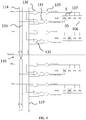
- figure 4 illustrates the pixel controller of figure 3 in more detail.
- first pixels 106 are represented by blocks P1-P4 without pattern
- second pixels 107 are represented by blocks P1-P4 with a pattern.
- figure 4 illustrates a total of four second pixels 107.
- each stitching block of pixels is associated with two pixel select sub-controller blocks 108.
- figure 4 only illustrates a single pixel select sub-controller block for each stitching block.
- Each pixel select sub-controller block has an identical structure.
- Each blocks comprises two AND gates 130 that are fed with a row select signal VRS Y+1 , VRS Y , which is generated in a shift register located inside pixel select sub-controller block 108 itself, and a global select signal that is fed using a line 117 that is connected to timing generator 113.
- line 117 is formed using line segments that are formed using reticle block 103 and that are stitched together to form a single line. The same holds for dose select lines 114, 115.
- Each pixel select sub-controller block 108 further comprises two OR gates 132 and two AND gates 131. The output of these logic gates is fed to a buffer 133 to provide sufficient signal strength for controlling the connected pixels.
- the dashed line corresponds to the stitching line. Consequently, the layout above and below the stitching line is identical as both parts are formed using the same reticle block(s). Consequently, in each column of pixels, two second pixels 107 may be identified, which normally would require two separate addressing steps to read out. Despite the fact that the layout above and below the stitching line is identical, the present invention allows the use of only a single second pixel 107 for each column for dose sensing purposes. This will be explained next.
- a dose select line connecting unit 116 is arranged to facilitate the coupling between dose select lines 114, 115 in the stitching blocks.
- the invention proposes to switch these signals. More in particular, dose select lines 114, 115 may be arranged in a given order that is identical for each stitching block. Each dose select line 114, 115 may then be associated with a given position in that order. For example, dose select line 114 is arranged to the left and dose select line 115 to the right.
- dose select line connecting unit 116 is to connect lines from different stitching blocks having a different position in those blocks.
- the dose select line on the left, i.e. line 114, in the top block is connected to the dose select line on the right in the bottom block, i.e. line 115.
- the dose select line on the right in the top block i.e. line 115, is connected to the dose select line on the left, i.e. line 114 in the bottom block.
- OR gate 132 of pixel select sub-controller block 108 is connected to dose select line 114, whereas the other OR gate 132 of the same other pixel select sub-controller block 108 is connected to dose select line 115.
- the output of OR gate 132 is fed to an AND gate 131 which also receives the global select signal on line 117.
- the output of AND gate 131 is fed to a buffer 133, which feeds the outputted signal to the second pixels 107 that are arranged in that row.
- each pixel select sub-controller block 108 is connected to two second pixels 107.
- the output of each AND gate 10 is fed to the first pixels 106 that are arranged in that row.
- a similar pixel select sub-controller block 108 may be arranged in each stitching block for selecting pixels P3 and P4. The difference between such block and the block shown in figure 4 would be that the output of AND gates 131 is not connected to P1 and P2 but to P3 and P4.
- the signal level on dose select line 115 is kept at ground potential, whereas the signals on lines 114 and 117 are controlled by timing generator 113.
- the shift registers of pixel select sub-controller blocks 108 output a low logical signal.
- a global reset is performed setting the photo-voltages in each pixel 106, 107 to a predefined voltage.
- a high logical signal may be put onto dose select line 114 of the bottom stitching block. Consequently, the first pixel P1 in the top row (first row) and the third pixel P3 of the third row of the bottom stitching block will be selected when the global select signal on line 117 is high.
- no second pixel will be selected. Due to the dose select connection unit 116, the signals in the top stitching block will be reversed.
- the signal on line 115 will be at the high logical level.
- the second pixel P2 in the second row and the fourth pixel P4 in the bottom row of that block will be selected.
- these pixels are situated in different columns than the pixels P1 and P3 selected in the bottom stitching block, a situation is prevented in which two or more second pixels can be selected in the same column.
- second pixels P1-P4 can be simultaneously read out.
- an artificial pixel may be used similar to the pixel shown in figure 2 albeit without a photodiode.
- this pixel which is typically arranged only in the bottom stitching block, the reference voltage is fed via the source follower onto the column line.
- read-out circuitry 106 the read-out from a second pixel in a given column is subtracted from the output of the artificial pixel to form a pixel voltage.
- the use of an artificial pixel allows some offset errors, such as those associated with the source follower, to be eliminated.
- the pixel voltages associated with P1-P4 are above a given threshold, it may be determined that the X-ray source or other light source has started to emit radiation or light onto the image sensor and that the image sensor should switch to the image read-out mode.
- the shift registers of pixel select sub-controller blocks 108 sequentially output a high logical signal.
- first VRS Y in the bottom pixel select sub-controller block 108 of bottom stitching block will be high (not shown), then VRS Y+1 in that same block 108, thereafter VRS Y in the top pixel select sub-controller block 108 of bottom stitching block, then VRS Y+1 in that same block 108, thereafter VRS Y in the bottom pixel select sub-controller block 108 of top stitching block (not shown), then VRS Y+1 in that same block 108, thereafter VRS Y in the top pixel select sub-controller block 108 of top stitching block, then VRS Y+1 in that same block 108.
- a pixel voltage will be determined in the image read-out mode as was explained in conjunction with figure 2 . More in particular, each reading cycle of a row of pixels will start with a reset after which charges may be collected by the storage capacitor during the integration time. After this time has elapsed, the row of pixels will be read out and a respective photo-voltage will be stored as a first voltage for each column. Next, the pixels of that row will be reset and the photo-voltage of each pixel will be directly read out and stored as the second voltage. The pixel voltage for a given pixel may then be determined by subtracting the first voltage from the second pixel.
- each row of pixels can be individually selected to be read out. Accordingly, the present invention allows the image sensor to operate in a dose sensing mode, wherein some pixels are selected and read out simultaneously for each stitching block, and in a image readout mode, wherein every pixel in a given row of a given stitching block is selected and read out simultaneously, despite the fact that the image sensor is comprised of a plurality of identical stitching blocks that are arranged in the column direction.
- Figure 5 illustrates an X-ray imaging system comprising an X-ray source 210, an X-ray detector 200 comprising an image sensor according to the invention, and an image processing unit 220 for constructing an X-ray image based on read-outs of X-ray detector 200.
- the X-ray source 210 need not be synchronized with X-ray detector 200.
- the image sensor comprised in detector 200 may be set to operate in the dose sensing mode, in response to a user input or automatically. In this mode, the second pixels will be read out. Any suitable mathematical operation can be used to determine whether the image read-out mode should be triggered. For example, the average dose among the second pixels may be determined and compared to a predefined threshold. Here, the dose received by a given pixel may be determined using the pixel voltage.
- X-ray detector 200 will collect image information in a manner known in the art.
- This image information comprising pixel voltages for each pixel in the pixel matrix, is provided to image processing unit 220 that constructs an image based on this information.
- the present invention equally relates to an optical system in which the X-ray detector 200 is replaced by an optical detector in which the image sensor of the present invention has been implemented. In this case, the scintillator layer will be omitted.
- the X-ray source 210 may be replaced by a light source, such as a source for emitting flashes light.
- the present invention allows the use of large, multi-stitching block image sensors to be used in non-synchronized X-ray systems without exposing the patient to too much X-ray radiation that is not used for the image formation.
- the X-ray dose to which the patient will be subjected to will be used as efficiently as possible.
Landscapes
- Engineering & Computer Science (AREA)
- Multimedia (AREA)
- Signal Processing (AREA)
- Physics & Mathematics (AREA)
- Health & Medical Sciences (AREA)
- Life Sciences & Earth Sciences (AREA)
- General Physics & Mathematics (AREA)
- High Energy & Nuclear Physics (AREA)
- Molecular Biology (AREA)
- Spectroscopy & Molecular Physics (AREA)
- Transforming Light Signals Into Electric Signals (AREA)
- Solid State Image Pick-Up Elements (AREA)
Claims (15)
- Capteur d'image (100), comprenant :
une matrice de rangées et colonnes de pixels photosensibles (106, 107), dans lequel la matrice comprend :une pluralité de blocs de base qui sont agencés de manière adjacente dans la direction de colonne de la matrice ;dans lequel chaque bloc de base comprend :une pluralité de premiers pixels (106) et une pluralité de seconds pixels (107) ;une pluralité de lignes de sélection de dose (114, 115) configurées de manière à transférer des signaux de sélection de dose respectifs ; etune unité de commande de sélection de pixel configurée de manière à :dans un mode de lecture d'image du capteur d'image, sélectionner simultanément des premiers pixels (106) et des seconds pixels (107), sur une rangée donnée et un bloc de base donné, une rangée à la fois ;dans un mode de détection de dose du capteur d'image (100), sélectionner simultanément des seconds pixels (107) sur différentes rangées et différents blocs de base en fonction des signaux de sélection de dose ;le capteur d'image (100) comprenant, en outre, à chaque interface de liaison entre les blocs de base qui sont agencés de manière adjacente dans la direction de colonne, une unité de liaison de ligne de sélection de dose (116) destinée à raccorder chaque ligne de sélection de dose (114, 115) d'un premier bloc de base parmi les différents blocs de base adjacents à une ligne de sélection de dose respective d'un second bloc de base parmi les blocs de base adjacents afin d'empêcher la sélection de seconds pixels multiples (107) sur la même colonne de la matrice. - Capteur d'image (100) selon la revendication 1, dans lequel chaque bloc de base est identique, dans lequel chaque bloc de base a, de préférence, été formé en utilisant la lithographie pas à pas de plaquette sur la base du ou des blocs de réticule (103).
- Capteur d'image (100) selon l'une quelconque des revendications précédentes, dans lequel les colonnes de chaque bloc de base comprennent au moins un second pixel (107).
- Capteur d'image (100) selon l'une quelconque des revendications précédentes, dans lequel chaque bloc de base comprend :une première partie agencée sur un premier côté du bloc de base, et une seconde partie agencée sur un second côté du bloc de base opposé au premier côté, dans lequel l'unité de liaison de ligne de sélection de dose (116) au niveau d'une interface entre une paire de blocs de base agencée de manière adjacente comprend la première partie d'un premier bloc de base parmi les blocs de base agencés de manière adjacente et la seconde partie de l'autre bloc de base parmi les blocs de base agencés de manière adjacente ; ouune unité de liaison de ligne de sélection de dose (116) respective agencée sur un premier côté du bloc de base.
- Capteur d'image (100) selon l'une quelconque des revendications précédentes, dans lequel les lignes de sélection de dose (114, 115) sont agencées de manière adjacente dans la direction de rangée de la matrice suivant un ordre donné, chaque ligne de sélection de dose (114, 115) présentant une position donnée suivant ledit ordre, dans lequel la position d'une ligne de sélection de dose (114, 115) dans un bloc de base donné est différente de la position de la ligne de sélection de dose dans le bloc de base agencé de manière adjacente auquel elle est raccordée.
- Capteur d'image (100) selon l'une quelconque des revendications précédentes,
dans lequel l'unité de commande de sélection de pixel est configurée de manière à sélectionner les premiers pixels (106) et les seconds pixels (107) dans le mode de lecture d'image en fonction d'un signal de sélection global et d'un signal de sélection de rangée spécifique à la rangée ; et
dans lequel l'unité de commande de sélection de pixel est configurée de manière à sélectionner les seconds pixels (107) dans le mode de détection de dose en fonction du signal de sélection global et des signaux de sélection de dose ;
le capteur d'image (100) comprenant, en outre, de préférence :un dispositif d'attaque de rangé contenu, de préférence, dans l'unité de commande de sélection de pixel, et configuré de manière à produire le signal de sélection de rangée spécifique à la rangée afin de sélectionner des pixels qui sont sur la même rangée ; etun générateur de séquence (113) destiné à produire le signal de sélection global, et au moins l'un des signaux de sélection de dose. - Capteur d'image (100) selon l'une quelconque des revendications précédentes, dans lequel un niveau d'un ou plusieurs des signaux de sélection de dose peut être commandé entre un niveau bas et un niveau haut, et dans lequel les autres signaux de sélection de dose présentent un niveau fixe, dans lequel la ou les lignes de sélection de dose (114, 115) sur chaque bloc de base, sur lesquelles lignes de sélection de dose (114, 115) le niveau peut être commandé, sont, de préférence, configurées afin de produire un signal de sélection de dose destiné à sélectionner un motif des seconds pixels (107) sur ce bloc de base dans le mode de détection de dose, dans lequel les motifs des seconds pixels (107) pour différents blocs de base sont différents, et dans lequel les motifs de seconds pixels (107) de différents blocs de base sont, de préférence, décalés dans la direction de rangée l'un par rapport à l'autre.
- Capteur d'image (100) selon l'une quelconque des revendications précédentes, dans lequel l'unité de commande de sélection de pixel comprend une pluralité de blocs d'unité de commande secondaire de sélection de pixels identiques (108) qui sont agencés de manière adjacente dans la direction de colonne et dans lequel chaque bloc d'unité de commande secondaire de sélection de pixels (108) est configuré, dans le mode de détection de dose, de manière à sélectionner un parmi n seconds pixels (107) qui sont agencés sur des rangées respectives et de préférence adjacentes, dans lequel n correspond au nombre de blocs de base qui sont agencés de manière adjacente dans la direction de colonne.
- Capteur d'image (100) selon l'une quelconque des revendications précédentes, dans lequel le nombre de blocs de base agencés de manière adjacente dans la direction de colonne est égal au nombre de lignes de sélection de dose (114, 115).
- Capteur d'image (100) selon l'une quelconque des revendications précédentes, comprenant, en outre, des circuits de lecture (109) destinés à lire les tensions photoélectriques de sortie des pixels photosensibles, lesdits circuits de lecture (109) étant raccordés à une pluralité de lignes de colonne qui sont chacune agencées sur chaque bloc de base, chaque ligne de colonne étant raccordée à une pluralité de pixels (106, 107) qui sont agencés sur la même colonne mais sur différentes rangées.
- Capteur d'image (100) selon la revendication 10, dans lequel chacun des premiers et seconds pixels (106, 107) comprend :une photodiode (21) destinée à produire un courant photoélectrique ;un condensateur de stockage (22, 23) dont une borne est raccordée à la photodiode (21), la tension au niveau de la borne étant définie comme ladite tension photoélectrique ;un transistor de réinitialisation (25) destiné à réinitialiser la tension au niveau de la borne à une tension prédéfinie ;un transistor de sélection (27) destiné à sélectionner le pixel (20) en fonction d'un signal de sélection de pixel ;un élément suiveur de source (26) destiné à délivrer la tension photoélectrique à la ligne de colonne à laquelle il est raccordé lorsque le pixel (20) est sélectionné.
- Capteur d'image (100) selon la revendication 10 ou 11, dans lequel :
le capteur d'image (100) est configuré de manière à exécuter un principe d'échantillonnage corrélé, dans lequel la lecture d'une tension photoélectrique d'un pixel (106, 107) dans le mode de lecture d'image comprend :une première étape de lecture dans laquelle la tension photoélectrique du pixel (106, 107) est réinitialisée à une valeur prédéfinie et est ensuite amenée, pendant un temps d'intégration, à varier en réponse à une dose de photons incidents, la tension photoélectrique étant lue en tant que première tension après expiration du temps d'intégration ;une seconde étape de lecture dans laquelle la tension photoélectrique du pixel (106, 107) est réinitialisée à la valeur prédéfinie et est ensuite lue directement en tant que deuxième tension ;dans lequel les circuits de lecture (109) sont configurés de manière à calculer une tension de pixel par soustraction de la première tension par rapport à la deuxième tension ; et/oudans lequel le capteur d'image est configuré de manière à exécuter un principe d'échantillonnage corrélé, dans lequel la lecture d'une tension photoélectrique d'un second pixel (107) dans le mode de détection de dose comprend :une étape de réinitialisation de la tension photoélectrique du pixel (106, 107) à une valeur prédéfinie ;une étape de lecture destinée à lire la tension photoélectrique en tant que troisième tension ;dans lequel les circuits de lecture (109) sont configurés de manière à calculer une tension de pixel par soustraction de la troisième tension par rapport à la tension prédéfinie. - Capteur d'image (100) selon l'une quelconque des revendications précédentes, dans lequel le capteur d'image (100) est configuré de manière à commuter ou à être commuté à partir du mode de détection de dose vers le mode de lecture d'image lorsque la dose déterminée dans le mode de détection de dose excède un seuil prédéfini.
- Capteur d'image (100) selon l'une quelconque des revendications précédentes, dans lequel le capteur d'image (100) est un capteur à rayon X dans lequel la matrice de pixels (106, 107) comprend une couche de scintillateur destinée à convertir un photon de rayon X entrant en photon de lumière visible.
- Dispositif d'imagerie par rayon X, comprenant :une source de rayon X (210) ;un capteur de rayon X (200) comprenant le capteur d'image (100) selon l'une quelconque des revendications précédentes ;une unité de traitement d'image (220) destinée à construire une image par rayon X sur la base des lectures du capteur de rayon X (200).
Priority Applications (2)
| Application Number | Priority Date | Filing Date | Title |
|---|---|---|---|
| EP18161290.4A EP3540469B1 (fr) | 2018-03-12 | 2018-03-12 | Capteur d'images |
| US16/299,043 US10978502B2 (en) | 2018-03-12 | 2019-03-11 | Image sensor |
Applications Claiming Priority (1)
| Application Number | Priority Date | Filing Date | Title |
|---|---|---|---|
| EP18161290.4A EP3540469B1 (fr) | 2018-03-12 | 2018-03-12 | Capteur d'images |
Publications (2)
| Publication Number | Publication Date |
|---|---|
| EP3540469A1 EP3540469A1 (fr) | 2019-09-18 |
| EP3540469B1 true EP3540469B1 (fr) | 2021-01-27 |
Family
ID=61626994
Family Applications (1)
| Application Number | Title | Priority Date | Filing Date |
|---|---|---|---|
| EP18161290.4A Active EP3540469B1 (fr) | 2018-03-12 | 2018-03-12 | Capteur d'images |
Country Status (2)
| Country | Link |
|---|---|
| US (1) | US10978502B2 (fr) |
| EP (1) | EP3540469B1 (fr) |
Families Citing this family (3)
| Publication number | Priority date | Publication date | Assignee | Title |
|---|---|---|---|---|
| US11721710B2 (en) * | 2019-12-30 | 2023-08-08 | Semiconductor Components Industries, Llc | Stitched integrated circuit dies |
| EP3885832B1 (fr) * | 2020-03-24 | 2024-05-08 | Imasenic Advanced Imaging, S.L. | Dispositif de capteur |
| US11438574B2 (en) * | 2020-10-26 | 2022-09-06 | Semiconductor Components Industries, Llc | Stitched integrated circuit dies |
Family Cites Families (14)
| Publication number | Priority date | Publication date | Assignee | Title |
|---|---|---|---|---|
| US6022649A (en) * | 1998-09-21 | 2000-02-08 | Chartered Semiconductor Manufacturing, Ltd. | Wafer stepper method utilizing a multi-segment global alignment mark |
| WO2002025314A1 (fr) * | 2000-09-20 | 2002-03-28 | Koninklijke Philips Electronics N.V. | Commande d'exposition dans un detecteur d'image a rayons x |
| GB0212001D0 (en) * | 2002-05-24 | 2002-07-03 | Koninkl Philips Electronics Nv | X-ray image detector |
| US7659516B2 (en) * | 2006-06-29 | 2010-02-09 | Dalsa Corporation | C-MOS sensor readout from multiple cells across the array to generate dose sensing signal |
| JP5766710B2 (ja) * | 2010-10-26 | 2015-08-19 | 富士フイルム株式会社 | 放射線画像撮影装置およびプログラム |
| JP5592962B2 (ja) * | 2012-02-03 | 2014-09-17 | 富士フイルム株式会社 | 放射線撮影装置とその制御方法、及び放射線撮影システム |
| JP5975733B2 (ja) * | 2012-05-25 | 2016-08-23 | 富士フイルム株式会社 | 放射線画像検出装置およびその駆動制御方法、並びに放射線撮影システム |
| GB2504111A (en) * | 2012-07-18 | 2014-01-22 | Stfc Science & Technology | Image sensor device with external addressing and readout circuitry located along same edge of the sensor device |
| JP5984306B2 (ja) * | 2012-08-22 | 2016-09-06 | 富士フイルム株式会社 | 放射線撮影システムおよびこれに用いられる信号中継装置 |
| JP2014045938A (ja) * | 2012-08-31 | 2014-03-17 | Fujifilm Corp | 放射線撮影システムおよびその通信方法、並びに放射線画像検出装置 |
| FR3013175B1 (fr) * | 2013-11-08 | 2015-11-06 | Trixell | Circuit integre presentant plusieurs blocs identiques identifies |
| KR101541123B1 (ko) * | 2013-11-29 | 2015-08-03 | (주)실리콘화일 | 이미지 시그널 프로세서의 이미지 데이터 출력 장치 |
| WO2015199612A1 (fr) * | 2014-06-25 | 2015-12-30 | Agency For Science, Technology And Research | Agencement de pixels |
| JP6385179B2 (ja) * | 2014-07-18 | 2018-09-05 | キヤノン株式会社 | 放射線撮像装置及びその駆動方法 |
-
2018
- 2018-03-12 EP EP18161290.4A patent/EP3540469B1/fr active Active
-
2019
- 2019-03-11 US US16/299,043 patent/US10978502B2/en active Active
Non-Patent Citations (1)
| Title |
|---|
| None * |
Also Published As
| Publication number | Publication date |
|---|---|
| EP3540469A1 (fr) | 2019-09-18 |
| US10978502B2 (en) | 2021-04-13 |
| US20190280028A1 (en) | 2019-09-12 |
Similar Documents
| Publication | Publication Date | Title |
|---|---|---|
| KR101425694B1 (ko) | 다중 프레임 캡처용 이미징 어레이 | |
| US7079189B2 (en) | Image sensing apparatus | |
| US7605376B2 (en) | CMOS sensor adapted for dental x-ray imaging | |
| EP0646305B1 (fr) | Procede et appareil de compensation par decalage pour detecteur de lumiere | |
| TWI441512B (zh) | 影像取得裝置及照相機系統 | |
| CA2293497C (fr) | Systeme de detection par rayons x utilisant des capteurs a pixels actifs | |
| RU2540980C2 (ru) | Устройство формирования изображения и система камеры | |
| EP1228384B1 (fr) | Commande d'exposition dans un détecteur d'image à rayons X | |
| CN101960331B (zh) | X射线探测器及其直接探测事件的抑制方法 | |
| JP2003517787A (ja) | イメージセンサ | |
| US6798864B2 (en) | Methods and apparatus for providing signal dependent offset and gain adjustments for a solid state X-ray detector | |
| KR20140000477A (ko) | 엑스레이 검출기, 엑스레이 검출기를 포함하는 엑스레이 촬영 시스템 및 엑스레이 검출기 구동 방법 | |
| US10978502B2 (en) | Image sensor | |
| CN106572822A (zh) | 辐射检测器以及使用辐射检测器的射线照相方法 | |
| JP7641721B2 (ja) | アクティブ画素口腔内放射線画像センサおよび関連する画像撮影方法 | |
| CN100498378C (zh) | 具有光栅和剂量控制的x射线检测器 | |
| WO2005107242A1 (fr) | Dispositif d'analyse aux rayons x et detecteur de rayonnement | |
| US20100019176A1 (en) | Imaging apparatus | |
| JP7190913B2 (ja) | 放射線撮像装置および放射線撮像システム | |
| US11013484B2 (en) | Dose sensing pixels reference voltage | |
| CN113711085B (zh) | 放射线检测器 | |
| KR101026923B1 (ko) | 가변 해상도 광자 계수형 엑스선 독출 방법, 독출 집적 회로 및 이미지 센서 | |
| JP7769662B2 (ja) | 放射線撮像装置、その制御方法及び放射線撮像システム | |
| JP2025099502A (ja) | 放射線撮像装置、および、放射線撮像システム | |
| JP2024004308A (ja) | 放射線撮像装置、放射線撮像システム、放射線撮像装置の制御方法、信号処理装置、信号処理装置の制御方法、および、プログラム |
Legal Events
| Date | Code | Title | Description |
|---|---|---|---|
| PUAI | Public reference made under article 153(3) epc to a published international application that has entered the european phase |
Free format text: ORIGINAL CODE: 0009012 |
|
| STAA | Information on the status of an ep patent application or granted ep patent |
Free format text: STATUS: THE APPLICATION HAS BEEN PUBLISHED |
|
| AK | Designated contracting states |
Kind code of ref document: A1 Designated state(s): AL AT BE BG CH CY CZ DE DK EE ES FI FR GB GR HR HU IE IS IT LI LT LU LV MC MK MT NL NO PL PT RO RS SE SI SK SM TR |
|
| AX | Request for extension of the european patent |
Extension state: BA ME |
|
| STAA | Information on the status of an ep patent application or granted ep patent |
Free format text: STATUS: REQUEST FOR EXAMINATION WAS MADE |
|
| 17P | Request for examination filed |
Effective date: 20200318 |
|
| RBV | Designated contracting states (corrected) |
Designated state(s): AL AT BE BG CH CY CZ DE DK EE ES FI FR GB GR HR HU IE IS IT LI LT LU LV MC MK MT NL NO PL PT RO RS SE SI SK SM TR |
|
| REG | Reference to a national code |
Ref country code: DE Ref legal event code: R079 Ref document number: 602018012158 Country of ref document: DE Free format text: PREVIOUS MAIN CLASS: G01T0001170000 Ipc: H04N0005320000 |
|
| RIC1 | Information provided on ipc code assigned before grant |
Ipc: H04N 5/32 20060101AFI20200730BHEP Ipc: G01T 1/17 20060101ALI20200730BHEP |
|
| GRAP | Despatch of communication of intention to grant a patent |
Free format text: ORIGINAL CODE: EPIDOSNIGR1 |
|
| STAA | Information on the status of an ep patent application or granted ep patent |
Free format text: STATUS: GRANT OF PATENT IS INTENDED |
|
| INTG | Intention to grant announced |
Effective date: 20200916 |
|
| GRAS | Grant fee paid |
Free format text: ORIGINAL CODE: EPIDOSNIGR3 |
|
| GRAA | (expected) grant |
Free format text: ORIGINAL CODE: 0009210 |
|
| STAA | Information on the status of an ep patent application or granted ep patent |
Free format text: STATUS: THE PATENT HAS BEEN GRANTED |
|
| AK | Designated contracting states |
Kind code of ref document: B1 Designated state(s): AL AT BE BG CH CY CZ DE DK EE ES FI FR GB GR HR HU IE IS IT LI LT LU LV MC MK MT NL NO PL PT RO RS SE SI SK SM TR |
|
| REG | Reference to a national code |
Ref country code: GB Ref legal event code: FG4D |
|
| REG | Reference to a national code |
Ref country code: CH Ref legal event code: EP |
|
| REG | Reference to a national code |
Ref country code: AT Ref legal event code: REF Ref document number: 1359370 Country of ref document: AT Kind code of ref document: T Effective date: 20210215 |
|
| REG | Reference to a national code |
Ref country code: IE Ref legal event code: FG4D |
|
| REG | Reference to a national code |
Ref country code: DE Ref legal event code: R096 Ref document number: 602018012158 Country of ref document: DE |
|
| REG | Reference to a national code |
Ref country code: NL Ref legal event code: MP Effective date: 20210127 |
|
| REG | Reference to a national code |
Ref country code: LT Ref legal event code: MG9D |
|
| REG | Reference to a national code |
Ref country code: AT Ref legal event code: MK05 Ref document number: 1359370 Country of ref document: AT Kind code of ref document: T Effective date: 20210127 |
|
| PG25 | Lapsed in a contracting state [announced via postgrant information from national office to epo] |
Ref country code: NO Free format text: LAPSE BECAUSE OF FAILURE TO SUBMIT A TRANSLATION OF THE DESCRIPTION OR TO PAY THE FEE WITHIN THE PRESCRIBED TIME-LIMIT Effective date: 20210427 Ref country code: PT Free format text: LAPSE BECAUSE OF FAILURE TO SUBMIT A TRANSLATION OF THE DESCRIPTION OR TO PAY THE FEE WITHIN THE PRESCRIBED TIME-LIMIT Effective date: 20210527 Ref country code: HR Free format text: LAPSE BECAUSE OF FAILURE TO SUBMIT A TRANSLATION OF THE DESCRIPTION OR TO PAY THE FEE WITHIN THE PRESCRIBED TIME-LIMIT Effective date: 20210127 Ref country code: FI Free format text: LAPSE BECAUSE OF FAILURE TO SUBMIT A TRANSLATION OF THE DESCRIPTION OR TO PAY THE FEE WITHIN THE PRESCRIBED TIME-LIMIT Effective date: 20210127 Ref country code: GR Free format text: LAPSE BECAUSE OF FAILURE TO SUBMIT A TRANSLATION OF THE DESCRIPTION OR TO PAY THE FEE WITHIN THE PRESCRIBED TIME-LIMIT Effective date: 20210428 Ref country code: LT Free format text: LAPSE BECAUSE OF FAILURE TO SUBMIT A TRANSLATION OF THE DESCRIPTION OR TO PAY THE FEE WITHIN THE PRESCRIBED TIME-LIMIT Effective date: 20210127 Ref country code: BG Free format text: LAPSE BECAUSE OF FAILURE TO SUBMIT A TRANSLATION OF THE DESCRIPTION OR TO PAY THE FEE WITHIN THE PRESCRIBED TIME-LIMIT Effective date: 20210427 |
|
| PG25 | Lapsed in a contracting state [announced via postgrant information from national office to epo] |
Ref country code: AT Free format text: LAPSE BECAUSE OF FAILURE TO SUBMIT A TRANSLATION OF THE DESCRIPTION OR TO PAY THE FEE WITHIN THE PRESCRIBED TIME-LIMIT Effective date: 20210127 Ref country code: RS Free format text: LAPSE BECAUSE OF FAILURE TO SUBMIT A TRANSLATION OF THE DESCRIPTION OR TO PAY THE FEE WITHIN THE PRESCRIBED TIME-LIMIT Effective date: 20210127 Ref country code: LV Free format text: LAPSE BECAUSE OF FAILURE TO SUBMIT A TRANSLATION OF THE DESCRIPTION OR TO PAY THE FEE WITHIN THE PRESCRIBED TIME-LIMIT Effective date: 20210127 Ref country code: PL Free format text: LAPSE BECAUSE OF FAILURE TO SUBMIT A TRANSLATION OF THE DESCRIPTION OR TO PAY THE FEE WITHIN THE PRESCRIBED TIME-LIMIT Effective date: 20210127 Ref country code: SE Free format text: LAPSE BECAUSE OF FAILURE TO SUBMIT A TRANSLATION OF THE DESCRIPTION OR TO PAY THE FEE WITHIN THE PRESCRIBED TIME-LIMIT Effective date: 20210127 |
|
| PG25 | Lapsed in a contracting state [announced via postgrant information from national office to epo] |
Ref country code: IS Free format text: LAPSE BECAUSE OF FAILURE TO SUBMIT A TRANSLATION OF THE DESCRIPTION OR TO PAY THE FEE WITHIN THE PRESCRIBED TIME-LIMIT Effective date: 20210527 |
|
| REG | Reference to a national code |
Ref country code: DE Ref legal event code: R097 Ref document number: 602018012158 Country of ref document: DE |
|
| PG25 | Lapsed in a contracting state [announced via postgrant information from national office to epo] |
Ref country code: SM Free format text: LAPSE BECAUSE OF FAILURE TO SUBMIT A TRANSLATION OF THE DESCRIPTION OR TO PAY THE FEE WITHIN THE PRESCRIBED TIME-LIMIT Effective date: 20210127 Ref country code: EE Free format text: LAPSE BECAUSE OF FAILURE TO SUBMIT A TRANSLATION OF THE DESCRIPTION OR TO PAY THE FEE WITHIN THE PRESCRIBED TIME-LIMIT Effective date: 20210127 Ref country code: CZ Free format text: LAPSE BECAUSE OF FAILURE TO SUBMIT A TRANSLATION OF THE DESCRIPTION OR TO PAY THE FEE WITHIN THE PRESCRIBED TIME-LIMIT Effective date: 20210127 Ref country code: MC Free format text: LAPSE BECAUSE OF FAILURE TO SUBMIT A TRANSLATION OF THE DESCRIPTION OR TO PAY THE FEE WITHIN THE PRESCRIBED TIME-LIMIT Effective date: 20210127 |
|
| REG | Reference to a national code |
Ref country code: CH Ref legal event code: PL |
|
| PG25 | Lapsed in a contracting state [announced via postgrant information from national office to epo] |
Ref country code: RO Free format text: LAPSE BECAUSE OF FAILURE TO SUBMIT A TRANSLATION OF THE DESCRIPTION OR TO PAY THE FEE WITHIN THE PRESCRIBED TIME-LIMIT Effective date: 20210127 Ref country code: DK Free format text: LAPSE BECAUSE OF FAILURE TO SUBMIT A TRANSLATION OF THE DESCRIPTION OR TO PAY THE FEE WITHIN THE PRESCRIBED TIME-LIMIT Effective date: 20210127 Ref country code: SK Free format text: LAPSE BECAUSE OF FAILURE TO SUBMIT A TRANSLATION OF THE DESCRIPTION OR TO PAY THE FEE WITHIN THE PRESCRIBED TIME-LIMIT Effective date: 20210127 |
|
| PLBE | No opposition filed within time limit |
Free format text: ORIGINAL CODE: 0009261 |
|
| STAA | Information on the status of an ep patent application or granted ep patent |
Free format text: STATUS: NO OPPOSITION FILED WITHIN TIME LIMIT |
|
| REG | Reference to a national code |
Ref country code: BE Ref legal event code: MM Effective date: 20210331 |
|
| 26N | No opposition filed |
Effective date: 20211028 |
|
| PG25 | Lapsed in a contracting state [announced via postgrant information from national office to epo] |
Ref country code: ES Free format text: LAPSE BECAUSE OF FAILURE TO SUBMIT A TRANSLATION OF THE DESCRIPTION OR TO PAY THE FEE WITHIN THE PRESCRIBED TIME-LIMIT Effective date: 20210127 Ref country code: CH Free format text: LAPSE BECAUSE OF NON-PAYMENT OF DUE FEES Effective date: 20210331 Ref country code: AL Free format text: LAPSE BECAUSE OF FAILURE TO SUBMIT A TRANSLATION OF THE DESCRIPTION OR TO PAY THE FEE WITHIN THE PRESCRIBED TIME-LIMIT Effective date: 20210127 Ref country code: LU Free format text: LAPSE BECAUSE OF NON-PAYMENT OF DUE FEES Effective date: 20210312 Ref country code: LI Free format text: LAPSE BECAUSE OF NON-PAYMENT OF DUE FEES Effective date: 20210331 Ref country code: IE Free format text: LAPSE BECAUSE OF NON-PAYMENT OF DUE FEES Effective date: 20210312 |
|
| PG25 | Lapsed in a contracting state [announced via postgrant information from national office to epo] |
Ref country code: SI Free format text: LAPSE BECAUSE OF FAILURE TO SUBMIT A TRANSLATION OF THE DESCRIPTION OR TO PAY THE FEE WITHIN THE PRESCRIBED TIME-LIMIT Effective date: 20210127 |
|
| PG25 | Lapsed in a contracting state [announced via postgrant information from national office to epo] |
Ref country code: IT Free format text: LAPSE BECAUSE OF FAILURE TO SUBMIT A TRANSLATION OF THE DESCRIPTION OR TO PAY THE FEE WITHIN THE PRESCRIBED TIME-LIMIT Effective date: 20210127 |
|
| PG25 | Lapsed in a contracting state [announced via postgrant information from national office to epo] |
Ref country code: IS Free format text: LAPSE BECAUSE OF FAILURE TO SUBMIT A TRANSLATION OF THE DESCRIPTION OR TO PAY THE FEE WITHIN THE PRESCRIBED TIME-LIMIT Effective date: 20210527 |
|
| PG25 | Lapsed in a contracting state [announced via postgrant information from national office to epo] |
Ref country code: BE Free format text: LAPSE BECAUSE OF NON-PAYMENT OF DUE FEES Effective date: 20210331 |
|
| PG25 | Lapsed in a contracting state [announced via postgrant information from national office to epo] |
Ref country code: NL Free format text: LAPSE BECAUSE OF NON-PAYMENT OF DUE FEES Effective date: 20210127 Ref country code: CY Free format text: LAPSE BECAUSE OF FAILURE TO SUBMIT A TRANSLATION OF THE DESCRIPTION OR TO PAY THE FEE WITHIN THE PRESCRIBED TIME-LIMIT Effective date: 20210127 |
|
| PG25 | Lapsed in a contracting state [announced via postgrant information from national office to epo] |
Ref country code: HU Free format text: LAPSE BECAUSE OF FAILURE TO SUBMIT A TRANSLATION OF THE DESCRIPTION OR TO PAY THE FEE WITHIN THE PRESCRIBED TIME-LIMIT; INVALID AB INITIO Effective date: 20180312 |
|
| PG25 | Lapsed in a contracting state [announced via postgrant information from national office to epo] |
Ref country code: MK Free format text: LAPSE BECAUSE OF FAILURE TO SUBMIT A TRANSLATION OF THE DESCRIPTION OR TO PAY THE FEE WITHIN THE PRESCRIBED TIME-LIMIT Effective date: 20210127 |
|
| PG25 | Lapsed in a contracting state [announced via postgrant information from national office to epo] |
Ref country code: TR Free format text: LAPSE BECAUSE OF FAILURE TO SUBMIT A TRANSLATION OF THE DESCRIPTION OR TO PAY THE FEE WITHIN THE PRESCRIBED TIME-LIMIT Effective date: 20210127 |
|
| PG25 | Lapsed in a contracting state [announced via postgrant information from national office to epo] |
Ref country code: MT Free format text: LAPSE BECAUSE OF FAILURE TO SUBMIT A TRANSLATION OF THE DESCRIPTION OR TO PAY THE FEE WITHIN THE PRESCRIBED TIME-LIMIT Effective date: 20210127 |
|
| PGFP | Annual fee paid to national office [announced via postgrant information from national office to epo] |
Ref country code: GB Payment date: 20260323 Year of fee payment: 9 |
|
| PGFP | Annual fee paid to national office [announced via postgrant information from national office to epo] |
Ref country code: DE Payment date: 20260313 Year of fee payment: 9 |
|
| PGFP | Annual fee paid to national office [announced via postgrant information from national office to epo] |
Ref country code: FR Payment date: 20260330 Year of fee payment: 9 |