EP3540801A1 - Dispositif à semi-conducteur et son procédé de réglage - Google Patents
Dispositif à semi-conducteur et son procédé de réglage Download PDFInfo
- Publication number
- EP3540801A1 EP3540801A1 EP19162903.9A EP19162903A EP3540801A1 EP 3540801 A1 EP3540801 A1 EP 3540801A1 EP 19162903 A EP19162903 A EP 19162903A EP 3540801 A1 EP3540801 A1 EP 3540801A1
- Authority
- EP
- European Patent Office
- Prior art keywords
- vertical hall
- hall element
- power source
- drive power
- current
- Prior art date
- Legal status (The legal status is an assumption and is not a legal conclusion. Google has not performed a legal analysis and makes no representation as to the accuracy of the status listed.)
- Granted
Links
- 239000004065 semiconductor Substances 0.000 title claims abstract description 56
- 238000000034 method Methods 0.000 title claims description 24
- 239000000758 substrate Substances 0.000 claims abstract description 14
- 230000007423 decrease Effects 0.000 claims description 2
- 238000009987 spinning Methods 0.000 description 13
- 238000006243 chemical reaction Methods 0.000 description 8
- 230000004907 flux Effects 0.000 description 7
- 238000010586 diagram Methods 0.000 description 6
- 238000004519 manufacturing process Methods 0.000 description 6
- 238000001514 detection method Methods 0.000 description 4
- 239000012535 impurity Substances 0.000 description 3
- 238000009792 diffusion process Methods 0.000 description 2
- 238000009826 distribution Methods 0.000 description 2
- 238000002955 isolation Methods 0.000 description 2
- 230000007704 transition Effects 0.000 description 2
- 230000003247 decreasing effect Effects 0.000 description 1
- 230000008054 signal transmission Effects 0.000 description 1
Images




Classifications
-
- G—PHYSICS
- G01—MEASURING; TESTING
- G01R—MEASURING ELECTRIC VARIABLES; MEASURING MAGNETIC VARIABLES
- G01R33/00—Arrangements or instruments for measuring magnetic variables
- G01R33/02—Measuring direction or magnitude of magnetic fields or magnetic flux
- G01R33/06—Measuring direction or magnitude of magnetic fields or magnetic flux using galvano-magnetic devices
- G01R33/07—Hall effect devices
- G01R33/077—Vertical Hall-effect devices
-
- G—PHYSICS
- G01—MEASURING; TESTING
- G01R—MEASURING ELECTRIC VARIABLES; MEASURING MAGNETIC VARIABLES
- G01R33/00—Arrangements or instruments for measuring magnetic variables
- G01R33/02—Measuring direction or magnitude of magnetic fields or magnetic flux
- G01R33/06—Measuring direction or magnitude of magnetic fields or magnetic flux using galvano-magnetic devices
- G01R33/07—Hall effect devices
- G01R33/072—Constructional adaptation of the sensor to specific applications
- G01R33/075—Hall devices configured for spinning current measurements
-
- H—ELECTRICITY
- H03—ELECTRONIC CIRCUITRY
- H03K—PULSE TECHNIQUE
- H03K3/00—Circuits for generating electric pulses; Monostable, bistable or multistable circuits
- H03K3/02—Generators characterised by the type of circuit or by the means used for producing pulses
- H03K3/353—Generators characterised by the type of circuit or by the means used for producing pulses by the use, as active elements, of field-effect transistors with internal or external positive feedback
- H03K3/356—Bistable circuits
- H03K3/3565—Bistables with hysteresis, e.g. Schmitt trigger
-
- H—ELECTRICITY
- H03—ELECTRONIC CIRCUITRY
- H03K—PULSE TECHNIQUE
- H03K5/00—Manipulating of pulses not covered by one of the other main groups of this subclass
- H03K5/22—Circuits having more than one input and one output for comparing pulses or pulse trains with each other according to input signal characteristics, e.g. slope, integral
- H03K5/24—Circuits having more than one input and one output for comparing pulses or pulse trains with each other according to input signal characteristics, e.g. slope, integral the characteristic being amplitude
-
- H—ELECTRICITY
- H10—SEMICONDUCTOR DEVICES; ELECTRIC SOLID-STATE DEVICES NOT OTHERWISE PROVIDED FOR
- H10N—ELECTRIC SOLID-STATE DEVICES NOT OTHERWISE PROVIDED FOR
- H10N52/00—Hall-effect devices
- H10N52/101—Semiconductor Hall-effect devices
Definitions
- the present invention relates to a semiconductor device and a method of adjusting the semiconductor device, and more particularly, to a semiconductor device including vertical Hall elements each configured to detect a magnetic field in a horizontal direction, and a method of adjusting the semiconductor device.
- a Hall element is capable of detecting position or angle without contact as a magnetic sensor, and accordingly has various uses. While magnetic sensors that use a horizontal Hall element configured to detect a magnetic field component perpendicular to a semiconductor substrate surface (vertical magnetic field) are particularly well known, there have also been proposed various magnetic sensors that use a vertical Hall element configured to detect a magnetic field component parallel to the semiconductor substrate surface (horizontal magnetic field).
- the vertical Hall element Since it is difficult to give a structure with high geometrical symmetry to a vertical Hall element, the vertical Hall element tends to generate a so-called offset voltage which is provided even at the absence of a magnetic field as compared with the horizontal Hall elements. In the use of the vertical Hall element as a magnetic sensor, the above-mentioned offset voltage should be removed.
- the spinning current method has been known as a method for removing such offset voltage.
- the resistances along the current paths are equal in any of the phases at the execution of the spinning current method, and hence the offset voltage can be accurately removed.
- the plurality of vertical Hall elements is formed simultaneously on the same substrate by a semiconductor manufacturing process, it is however extremely difficult to obtain totally the same impurity concentration distribution or the like in the plurality of vertical Hall elements. Accordingly, the plurality of vertical Hall elements has variations in the characteristics. The resistances along the current paths are therefore not totally equal in each phase at the execution of the spinning current method, and accuracy of offset cancellation is thus not improved much.
- a semiconductor device including, a first vertical Hall element provided in a first region of a semiconductor substrate, and including a first plurality of electrodes arranged at predetermined intervals on a first straight line, a second vertical Hall element provided in a second region of the semiconductor substrate which is different from the first region, and including a second plurality of electrodes of the same number as a number of the first plurality of electrodes, the second plurality of electrodes being arranged at the predetermined intervals on a second straight line parallel to the first straight line, a first drive power source configured to drive the first vertical Hall element, and a second drive power source configured to drive the second vertical Hall element and provided separately from the first drive power source.
- the first and second vertical Hall elements are independently driven by separate drive power sources.
- errors in characteristics of the first and second vertical Hall elements generated in a semiconductor manufacturing process can be compensated by appropriately adjusting the first and second drive power sources.
- the spinning current method can therefore be performed under a condition in which characteristics of the first and second vertical Hall elements are set substantially the same, and hence offset cancellation can be achieved with high accuracy.
- FIG. 1 and FIG. 2 are schematic diagrams for illustrating a semiconductor device including vertical Hall elements according to an embodiment of the present invention.
- a first case phase 1
- a second case phase 2
- a direction of the current flowing through each of the vertical Hall elements is set to be in a second condition at the execution of the spinning current method.
- the semiconductor device includes: a vertical Hall element 100 and a vertical Hall element 200; a current source 120 and a current source 220 serving as drive power sources configured to supply drive currents to the vertical Hall elements 100 and 200, respectively; an amplifier 110 and an amplifier 210 configured to amplify signals obtained from the vertical Hall elements 100 and 200, respectively; and switches S10 to S19 and S20 to S29 configured to switch directions of the currents for driving the vertical Hall elements 100 and 200, respectively.
- the vertical Hall elements 100 and 200 include five electrodes 111 to 115 and five electrodes 211 to 215 which are arranged at predetermined intervals on a straight line L1-L1 and a straight line L2-L2 illustrated in FIG. 1 , respectively, and have substantially the same structure. Further, the vertical Hall elements 100 and 200 are arranged such that the straight line L1-L1 and the straight line L2-L2 are parallel to each other.
- the current source 120 is configured to connect to the vertical Hall element 100 through the switches S10 to S14. That is, an input terminal of the current source 120 is connected to the electrode 111 through the switch S10, to the electrode 112 through the switch S11, and to the electrode 115 through the switch S14, and an output terminal of the current source 120 is connected to the electrode 113 through the switch S12 and to the electrode 114 through the switch S13.
- the current source 220 is configured to connect to the vertical Hall element 200 through the switches S20 to S24. That is, an input terminal of the current source 220 is connected to the electrode 213 through the switch S22 and to the electrode 214 through the switch S23, and an output terminal of the current source 220 is connected to the electrode 211 through the switch S20, to the electrode 212 through the switch S21, and to the electrode 215 through the switch S24.
- the amplifier 110 is configured to connect to the vertical Hall element 100 through the switches S15 to S19. That is, a non-inverting input terminal of the amplifier 110 is connected to the electrode 112 through the switch S16 and to the electrode 113 through the switch S17, and an inverting input terminal of the amplifier 110 is connected to the electrode 111 through the switch S15, to the electrode 114 through the switch S18, and to the electrode 115 through the switch S19.
- the amplifier 210 is configured to connect to the vertical Hall element 200 through the switches S25 to S29. That is, a non-inverting input terminal of the amplifier 210 is connected to the electrode 211 through the switch S25, to the electrode 214 through the switch S28, and to the electrode 215 through the switch S29, and an inverting input terminal of the amplifier 210 is connected to the electrode 212 through the switch S26 and to the electrode 213 through the switch S27.
- FIG. 3 is a view corresponding to a cross section taken along the line L-L of the semiconductor device illustrated in FIG. 1 .
- the vertical Hall elements 100 and 200 are formed in a region RA and a region RB of a P-type (first conductivity type) semiconductor substrate 101, respectively.
- the region RA and the region RB are electrically separated from each other by a P-type element isolation diffusion layer 103 formed in an N-type (second conductivity type) semiconductor layer 102 provided on the semiconductor substrate 101.
- the electrodes 111 to 115 of the vertical Hall element 100 and the electrodes 211 to 215 of the vertical Hall element 200 are formed by N-type impurity regions each having a higher concentration than that of the semiconductor layer 102 and being provided adjacent to a surface of the semiconductor layer 102 in each the regions RA and RB.
- the current sources 120 and 220, the amplifiers 110 and 210, and the switches S10 to S19 and S20 to S29 illustrated in FIG. 1 and FIG. 2 are also formed to be electrically separate from the vertical Hall elements 100 and 200 by the element isolation diffusion layers 103 on regions other than the regions RA and RB of the semiconductor substrate 101.
- FIG. 3 an example is illustrated in which the vertical Hall element 100 and the vertical Hall element 200 are arranged side by side in a lateral direction, that is, arranged such that the straight line L1-L1 and the straight line L2-L2 illustrated in FIG. 1 are on the same straight line.
- the vertical Hall element 100 and the vertical Hall element 200 may be arranged in any positions as long as the straight line L1-L1 and the straight line L2-L2 are arranged in parallel.
- the vertical Hall element 100 and the vertical Hall element 200 may be arranged in parallel in a vertical direction, that is, in FIG. 1 and FIG.
- the vertical Hall element 100 may be arranged on an upper side of the drawing sheet and the vertical Hall element 200 may be arranged on a lower side of the drawing sheet. Further, arrangement of the vertical Hall element 100 and the vertical Hall element 200 adjacent to each other is not necessarily required.
- the current sources 120 and 220 or the amplifiers 110 and 210 can also be arranged between the vertical Hall element 100 and the vertical Hall element 200.
- the switches S10, S12, S14, S16, and S18 connected to the vertical Hall element 100 and the switches S20, S22, S24, S26, and S28 connected to the vertical Hall element 200 are turned on, and the switches S11, S13, S15, S17, and S19 connected to the vertical Hall element 100 and the switches S21, S23, S25, S27, and S29 connected to the vertical Hall element 200 are turned off.
- the drive current is supplied from the current source 120 to the vertical Hall element 100 such that the current flows from the electrode 113 to the electrodes 111 and 115 at both ends (direction of the current at this time is referred to as "first current direction"), and a potential difference is generated between the electrode 112 and the electrode 114.
- the switches S16 and S18 are on, the non-inverting input terminal of the amplifier 110 is connected to the electrode 112, and the inverting input terminal is connected to the electrode 114.
- the amplifier 110 therefore amplifies the potential difference between the electrode 112 and the electrode 114 to output the amplified potential difference to an adder 130.
- the drive current is supplied from the current source 220 to the vertical Hall element 200 such that the current flows from the electrodes 211 and 215 at both ends to the electrode 213 (direction of the current at this time is referred to as "second current direction"), and a potential difference is generated between the electrode 212 and the electrode 214.
- the switches S26 and S28 are on, the non-inverting input terminal of the amplifier 210 is connected to the electrode 214, and the inverting input terminal is connected to the electrode 212.
- the amplifier 210 therefore amplifies the potential difference between the electrode 214 and the electrode 212 to output the amplified potential difference to the adder 130.
- the adder 130 adds the output signal from the amplifier 110 to the output signal from the amplifier 210, and provides an output voltage VOUT1 to an output terminal 131 as an output voltage of the phase 1.
- the output voltage VOUT1 is held by, for example, a sample-and-hold circuit (not shown).
- the switches S11, S13, S15, S17, and S19 connected to the vertical Hall element 100 and the switches S21, S23, S25, S27 and S29 connected to the vertical Hall element 200 are turned on, and the switches S10, S12, S14, S16, and S18 connected to the vertical Hall element 100 and the switches S20, S22, S24, S26, and S28 connected to the vertical Hall element 200 are turned off.
- the drive current is supplied from the current source 120 to the vertical Hall element 100 such that the current flows from the electrode 114 to the electrode 112 (direction of the current at this time is referred to as "third current direction"), and a potential difference is generated between the electrode 113 and the electrodes 111 and 115.
- the switches S15, S17, and S19 are turned on, the non-inverting input terminal of the amplifier 110 is connected to the electrode 113, and the inverting input terminal is connected to the electrodes 111 and 115.
- the amplifier 110 therefore amplifies the potential difference between the electrode 113 and the electrodes 111 and 115 to output the amplified potential difference to the adder 130.
- the drive current is supplied from the current source 220 to the vertical Hall element 200 such that the current flows from the electrode 212 to the electrode 214 (direction of the current at this time is referred to as "fourth current direction"), and a potential difference is generated between the electrodes 211 and 215 and the electrode 213.
- the switches S25, S27, and S29 are on, the non-inverting input terminal of the amplifier 210 is connected to the electrodes 211 and 215, and the inverting input terminal is connected to the electrode 213.
- the amplifier 210 therefore amplifies the potential difference between the electrodes 211, 215 and the electrode 213 to output the amplified potential difference to the adder 130.
- the adder 130 adds the output signal from the amplifier 110 to the output signal from the amplifier 210, and provides an output voltage VOUT2 to the output terminal 131 as an output voltage of the phase 2.
- the output voltage VOUT1 obtained in the phase 1 is subtracted from the output voltage VOUT2 obtained in the phase 2, thereby permitting attainment of the final output voltage from which the offset voltage is removed.
- the example is illustrated in which the drive current in the first current direction is supplied to the vertical Hall element 100 and the drive current in the second current direction is supplied to the vertical Hall element 200 in the phase 1, and the drive current in the third current direction is supplied to the vertical Hall element 100 and the drive current in the fourth current direction is supplied to the vertical Hall element 200 in the phase 2.
- the supply directions of the drive currents are not limited thereto.
- a switching method for the switches may be changed in the following manner, for example, in which the drive current in the first current direction may be supplied to the vertical Hall element 100 and the drive current in the fourth current direction may be supplied to the vertical Hall element 200 in the phase 1, and the drive current in the third current direction may be supplied to the vertical Hall element 100 and the drive current in the second current direction may be supplied to the vertical Hall element 200 in the phase 2.
- the supply directions of the drive currents are appropriately changeable, and the offset voltage may be canceled by appropriately adding or subtracting the output voltage obtained accordingly.
- the vertical Hall element 100 and the vertical Hall element 200 are simultaneously formed on the same semiconductor substrate in the semiconductor manufacturing process. However, realizing totally the same impurity concentration distribution or the like in the vertical Hall elements 100 and 200 is difficult. Variations in the characteristics are therefore generated between the vertical Hall element 100 and the vertical Hall element 200.
- the current source 120 and the current source 220 which are separately provided, drive the vertical Hall element 100 and the vertical Hall element 200, respectively.
- the drive current of the vertical Hall element 100 and the drive current of the vertical Hall element 200 can be separately adjusted.
- the current from the current source 120 and the current from the current source 220 are set in advance to have the same current value (referred to as initial current value), and output voltages of the vertical Hall element 100 and the vertical Hall element 200 are measured in supply of the drive current having the same direction and the same current value to each of the vertical Hall element 100 and the vertical Hall element 200. Then, based on a difference between the measured output voltages, the current values of the current source 120 and the current value of the current source 220 are adjusted so that the difference vanishes. In this manner, variation in the characteristics between the vertical Hall element 100 and the vertical Hall element 200 can be substantially compensated. Offset cancellation by the spinning current method can therefore be performed with high accuracy.
- each current value of the current source 120 and the current source 220 is adjusted by, for example, increasing the current value of the current source 120 by ⁇ from the initial current value and decreasing the current value of the current source 220 by ⁇ from the initial current value such that the total current value (drive current) is constant. In this manner, it is possible to eliminate the need to adjust the circuits such as the amplifiers 110 and 210 on output sides of the vertical Hall elements 100 and 200.
- the embodiment has the configuration in which the outputs of the vertical Hall elements 100 and 200 are amplified by the separate amplifiers 110 and 210, respectively. With this configuration, it is also possible to compensate variation in the characteristics between the vertical Hall element 100 and the vertical Hall element 200 by adjusting respective gains of the amplifiers 110 and 210.
- the output sides of the vertical Hall elements 100 and 200 may be appropriately connected, and an output voltage from the vertical Hall elements 100 and 200 may be amplified by a single amplifier.
- variation in the characteristics between the vertical Hall element 100 and the vertical Hall element 200 cannot be compensated by adjusting the gains of the two amplifiers 110 and 210 as described above, but the circuit can be downsized because of the single amplifier.
- a hysteresis characteristic can be added to the final output voltage by appropriately adjusting the drive currents supplied to the respective vertical Hall elements 100 and 200, that is, the current values of the current sources 120 and 220.
- the current values of the current sources 120 and 220 are adjusted so as to add a hysteresis characteristic to the final output voltage.
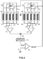
- FIG. 4 is a diagram for illustrating the specific configuration example in which a hysteresis characteristic is added to the final output voltage of the semiconductor device illustrated in FIG. 1 and FIG. 2 .
- FIG. 4 the same condition of the phase 1 as that in FIG. 1 is illustrated, while the condition of the phase 2 is the same as that in FIG. 2 , and hence illustration thereof is omitted.
- FIG. 5 is a graph for showing magnetoelectric conversion characteristic of the semiconductor device illustrated in FIG. 4 .
- the semiconductor device illustrated in FIG. 4 further includes, in addition to the configuration of the semiconductor device illustrated in FIG. 1 , a sample-and-hold circuit 140 and a comparator 150.
- the sample-and-hold circuit 140 holds the output voltage VOUT1 in the phase 1 described above, further subtracts the output voltage VOUT1 temporally held in the circuit from the output voltage VOUT2 in the phase 2, and provides the subtraction result as the final output voltage VOUT.
- the output voltage VOUT from the sample-and-hold circuit 140 is supplied to a non-inverting input terminal of the comparator 150, a ground voltage from a ground terminal 151 is supplied to an inverting input terminal of the comparator 150 as a reference voltage, and a result of comparison between the voltage VOUT and the ground voltage is provided as an output signal CMPOUT.
- the output signal CMPOUT from the comparator 150 is supplied to the current sources 120 and 220.
- the current values of the current sources 120 and 220 are adjusted in advance in order to compensate variation in the characteristics between the vertical Hall element 100 and the vertical Hall element 200.
- the current sources 120 and 220 are each configured to, based on the output signal CMPOUT from the comparator 150, switch the current value between two values with reference to the current value in the adjusted condition.
- the ground voltage (0 V) is supplied to the inverting input terminal of the comparator 150, and hence the comparator 150 provides the output signal CMPOUT corresponding to the voltage value of the voltage VOUT of the non-inverting input terminal as follows:
- the X-axis represents an applied magnetic flux density B
- the Y-axis represents the output voltage VOUT from the sample-and-hold circuit 140 (input voltage of the non-inverting input terminal of the comparator 150).
- the current values I1 and I2 can be defined as follows:
- the output voltage VOUT of the sample-and-hold circuit 140 can thus have magnetoelectric conversion characteristic composed from two lines which incline equally and whose Y-intercepts are each offset from the origin by ⁇ VOS.
- the constant ⁇ is a value adjusted in advance so as to compensate variation in the characteristics between the vertical Hall element 100 and the vertical Hall element 200.
- the value of ⁇ is set arbitrarily depending on a desired hysteresis width BHYS.
- the applied magnetic flux density B at this moment is an operating point BOP.
- the applied magnetic flux density B at this moment is a returning point BRP.
- providing the magnetoelectric conversion characteristics with the hysteresis characteristic can achieve an alternating detection characteristic having the hysteresis width BHYS. Since it is not required to provide a circuit or the like usually provided to add a hysteresis characteristic at a subsequent stage of the output of the sample-and-hold circuit 140 so as to switch signal transmission polarities of a signal path, and since it is only required to add a comparator having a simple configuration, hence an occupation area by the circuit can be reduced.
- a predetermined reference voltage VREF instead of the ground voltage may be supplied to the inverting input terminal of the comparator 150.
- an inversion level of the magnetoelectric conversion characteristics of the output voltage VOUT of the sample-and-hold circuit 140 of FIG. 5 is not 0 but VREF, the relation between the output voltage
- VOUT and the output signal CMPOUT becomes as follows:
- the operating point BOP and the returning point BRP are offset in accordance with the absolute value and the polarity of the predetermined reference voltage VREF. That is, if VREF (>0) is supplied such that the operating point BOP and the returning point BRP are both positive, then an S-pole detection characteristic having the operating point BOP and the returning point BRP on the S-pole side can be achieved. Further, if VREF ( ⁇ 0) is supplied such that the operating point BOP and the returning point BRP are both negative, then an N-pole detection characteristic having the operating point BOP and the returning point BRP on the N-pole side can be also achieved.
- FIG. 4 the example is illustrated in which the current values of both the current sources 120 and 220 are switched based on the output signal CMPOUT of the comparator 150.
- a configuration in which only one current value of the current source 120 or 220 is switched may be adopted.
- the current source 220 for driving the vertical Hall element 200 is provided separately from the current source 120 for driving the vertical Hall element 100.
- characteristic errors in the vertical Hall element 100 and the vertical Hall element 200 generated in a semiconductor manufacturing process can be compensated by appropriately adjusting the current values of the current source 120 and the current source 220.
- the spinning current method can be performed under a condition in which the characteristic of the vertical Hall element 100 and the characteristic of the vertical Hall element 200 are set to be substantially the same. Offset cancellation can therefore be performed with high accuracy.
- the final output voltage VOUT can be added with a hysteresis characteristic by controlling to switch the current values of the current source 120 and the current source 220 based on the output signal CMPOUT of the comparator 150. Since addition of a special circuit which is usually provided at a subsequent stage of the final output voltage VOUT so as to add a hysteresis characteristic is not required, hence the area of the entire semiconductor device can be reduced.
- the example using the current sources as driving power sources has been described, but voltage sources may be used instead of the current sources.
- the drive currents of the vertical Hall elements are adjusted by adjusting voltage values of the voltage sources.
- the semiconductor device including two vertical Hall elements has been described as an example, but the present invention is also applicable to a semiconductor device including three or more vertical Hall elements.
- the characteristic errors of the plurality of vertical Hall elements generated in the semiconductor manufacturing process can be corrected by providing the same number of drive power sources as the number of the plurality of vertical Hall elements and by driving each vertical Hall element by an independent drive power source.
- drive currents in the first to fourth current directions can be supplied to each vertical Hall element all at once, and hence time needed for offset cancellation can be shortened.
- drive currents in the four directions can be supplied to each of two vertical Hall elements, and hence more accurate offset cancellation can be achieved.
- the example has been described in which the amplifier 110 and the amplifier 210 are connected to the vertical Hall element 100 and the vertical Hall element 200, respectively, and the output signal of the amplifier 110 and the output signal of the amplifier 210 are added by the adder 130.
- the following configuration is also applicable. That is, a single amplifier is provided. First of all, under the condition illustrated in FIG. 1 , a difference between the output voltages obtained by driving the vertical Hall element 100 is amplified by the single amplifier to have the first output signal, and, under the condition illustrated in FIG. 1 , a difference between the output voltages obtained by driving the vertical Hall element 200 is amplified by the single amplifier to have the second output signal. Then, under the condition illustrated in FIG.
- a difference between the output voltages obtained by driving the vertical Hall element 100 is amplified by the single amplifier to have the third output signal
- a difference between the output voltages obtained by driving the vertical Hall element 200 is amplified by the single amplifier to have the fourth output signal.
- the first to fourth output signals are added or subtracted.
- time-division processing is used, the time needed for offset cancellation extends.
- the current directions of the currents supplied to the vertical Hall elements 100 and 200 are two directions. That is, the vertical Hall element 100 is supplied with the drive currents in the first and third current directions, and the vertical Hall element 200 is supplied with the drive currents in the second and fourth current directions.
- each of the vertical Hall elements 100 and 200 may be applied with the currents in the first to fourth current directions to perform offset cancellation. In this case, four phases are required, and hence the time needed for offset cancellation is increased, but the accuracy of offset cancellation can be improved.
- the vertical Hall elements 100 and 200 each have five electrodes, but the present invention is not limited thereto. As long as the vertical Hall element 100 has the same number of electrodes as that of the vertical Hall element 200, each element may have three or more electrodes. This also applies to a case in which the semiconductor device includes three or more vertical Hall elements.
- the first conductivity type is described as a P-type
- the second conductivity type is described as an N-type
- the conductivity types may be changed, that is, the first conductivity type may be an N-type, and the second conductivity type may be a P-type.
Landscapes
- Physics & Mathematics (AREA)
- Condensed Matter Physics & Semiconductors (AREA)
- General Physics & Mathematics (AREA)
- Nonlinear Science (AREA)
- Hall/Mr Elements (AREA)
- Measuring Magnetic Variables (AREA)
Applications Claiming Priority (2)
| Application Number | Priority Date | Filing Date | Title |
|---|---|---|---|
| JP2018046888 | 2018-03-14 | ||
| JP2018230554A JP7239308B2 (ja) | 2018-03-14 | 2018-12-10 | 半導体装置及びその調整方法 |
Publications (2)
| Publication Number | Publication Date |
|---|---|
| EP3540801A1 true EP3540801A1 (fr) | 2019-09-18 |
| EP3540801B1 EP3540801B1 (fr) | 2021-04-28 |
Family
ID=65861212
Family Applications (1)
| Application Number | Title | Priority Date | Filing Date |
|---|---|---|---|
| EP19162903.9A Active EP3540801B1 (fr) | 2018-03-14 | 2019-03-14 | Dispositif à semi-conducteur et son procédé de réglage |
Country Status (3)
| Country | Link |
|---|---|
| US (1) | US11016151B2 (fr) |
| EP (1) | EP3540801B1 (fr) |
| CN (1) | CN110277487B (fr) |
Families Citing this family (1)
| Publication number | Priority date | Publication date | Assignee | Title |
|---|---|---|---|---|
| TW202201038A (zh) * | 2020-03-13 | 2022-01-01 | 日商艾普凌科有限公司 | 半導體裝置 |
Citations (4)
| Publication number | Priority date | Publication date | Assignee | Title |
|---|---|---|---|---|
| EP1438755A2 (fr) | 2001-10-16 | 2004-07-21 | Fraunhofer-Gesellschaft zur Förderung der angewandten Forschung e.V. | Capteur vertical a effet hall |
| US20120286776A1 (en) * | 2011-02-08 | 2012-11-15 | Infineon Technologies Ag | Low Offset Vertical Hall Device and Current Spinning Method |
| US20130342194A1 (en) * | 2012-06-22 | 2013-12-26 | Infineon Technologies Ag | Vertical hall sensor with series-connected hall effect regions |
| US20140210461A1 (en) * | 2013-01-29 | 2014-07-31 | Infineon Technologies Ag | Vertical hall device with highly conductive opposite face node for electrically connecting first and second hall effect regions |
Family Cites Families (8)
| Publication number | Priority date | Publication date | Assignee | Title |
|---|---|---|---|---|
| JP4924308B2 (ja) * | 2004-11-12 | 2012-04-25 | 株式会社デンソー | 縦型ホール素子 |
| JP4674578B2 (ja) * | 2006-01-13 | 2011-04-20 | 株式会社デンソー | 磁気センサ及び磁気検出方法 |
| JP2008008883A (ja) * | 2006-06-02 | 2008-01-17 | Denso Corp | 磁気センサ及びセンサ |
| JP5052982B2 (ja) * | 2007-07-25 | 2012-10-17 | セイコーインスツル株式会社 | 磁気センサ回路 |
| EP2108966A1 (fr) * | 2008-04-08 | 2009-10-14 | Ecole Polytechnique Fédérale de Lausanne (EPFL) | Capteur de courant et module de construction pour mesure de courant |
| JP5865108B2 (ja) * | 2012-02-16 | 2016-02-17 | セイコーインスツル株式会社 | 磁気センサ装置 |
| US10386392B2 (en) * | 2015-01-28 | 2019-08-20 | Hioki Denki Kabushiki Kaisha | Hall element driving circuit, sensor circuit, and current measuring apparatus |
| CN106291412A (zh) * | 2015-05-26 | 2017-01-04 | 无锡艾柯威科技有限公司 | 一种霍尔电路及其信号输出方法 |
-
2019
- 2019-03-11 US US16/298,434 patent/US11016151B2/en active Active
- 2019-03-12 CN CN201910184094.5A patent/CN110277487B/zh active Active
- 2019-03-14 EP EP19162903.9A patent/EP3540801B1/fr active Active
Patent Citations (4)
| Publication number | Priority date | Publication date | Assignee | Title |
|---|---|---|---|---|
| EP1438755A2 (fr) | 2001-10-16 | 2004-07-21 | Fraunhofer-Gesellschaft zur Förderung der angewandten Forschung e.V. | Capteur vertical a effet hall |
| US20120286776A1 (en) * | 2011-02-08 | 2012-11-15 | Infineon Technologies Ag | Low Offset Vertical Hall Device and Current Spinning Method |
| US20130342194A1 (en) * | 2012-06-22 | 2013-12-26 | Infineon Technologies Ag | Vertical hall sensor with series-connected hall effect regions |
| US20140210461A1 (en) * | 2013-01-29 | 2014-07-31 | Infineon Technologies Ag | Vertical hall device with highly conductive opposite face node for electrically connecting first and second hall effect regions |
Also Published As
| Publication number | Publication date |
|---|---|
| CN110277487A (zh) | 2019-09-24 |
| EP3540801B1 (fr) | 2021-04-28 |
| US11016151B2 (en) | 2021-05-25 |
| CN110277487B (zh) | 2024-07-16 |
| US20190285708A1 (en) | 2019-09-19 |
Similar Documents
| Publication | Publication Date | Title |
|---|---|---|
| US20090009163A1 (en) | Magnetic sensing device and electronic compass using the same | |
| EP3176593B1 (fr) | Circuit de détection de signal de force électromotrice d'effet hall et capteur de courant | |
| US6984989B2 (en) | Current sensor and overload current protective device therewith | |
| US20050001613A1 (en) | Offset-reduced hall sensor | |
| KR101542679B1 (ko) | 자기 검출 장치 및 자기 검출 방법 | |
| US9128127B2 (en) | Sensor device | |
| HK1045562A1 (en) | Hall sensor array for measuring a magnetic field with offset compensation | |
| CN107076806A (zh) | 具有偏移补偿的霍尔效应传感器电路 | |
| CN105823918A (zh) | 霍尔元件驱动电路、传感器电路、及电流测定装置 | |
| CN108572338B (zh) | 磁传感器电路 | |
| KR102697502B1 (ko) | 반도체 장치 및 그 조정 방법 | |
| EP3540801B1 (fr) | Dispositif à semi-conducteur et son procédé de réglage | |
| KR102642649B1 (ko) | 반도체 장치 | |
| JP2011169696A (ja) | 磁気センサユニット | |
| KR20170061700A (ko) | 홀 센서 | |
| JPWO2017057650A1 (ja) | 磁場検知装置 | |
| JP2024115234A (ja) | 半導体装置 | |
| US12493056B2 (en) | Current detection apparatus and current detection method | |
| JP3819323B2 (ja) | ホール素子及び電気量測定装置 | |
| JP4108774B2 (ja) | ピーク検出回路 | |
| US20190326507A1 (en) | Semiconductor device | |
| US20160266215A1 (en) | Magnetic sensor device | |
| JPH02301151A (ja) | 電流検出機能付トランジスタ | |
| KR101820756B1 (ko) | 저항오차 보정기능을 갖는 홀 플레이트 | |
| JPH077047B2 (ja) | 磁気検出装置 |
Legal Events
| Date | Code | Title | Description |
|---|---|---|---|
| PUAI | Public reference made under article 153(3) epc to a published international application that has entered the european phase |
Free format text: ORIGINAL CODE: 0009012 |
|
| STAA | Information on the status of an ep patent application or granted ep patent |
Free format text: STATUS: THE APPLICATION HAS BEEN PUBLISHED |
|
| AK | Designated contracting states |
Kind code of ref document: A1 Designated state(s): AL AT BE BG CH CY CZ DE DK EE ES FI FR GB GR HR HU IE IS IT LI LT LU LV MC MK MT NL NO PL PT RO RS SE SI SK SM TR |
|
| AX | Request for extension of the european patent |
Extension state: BA ME |
|
| STAA | Information on the status of an ep patent application or granted ep patent |
Free format text: STATUS: REQUEST FOR EXAMINATION WAS MADE |
|
| STAA | Information on the status of an ep patent application or granted ep patent |
Free format text: STATUS: EXAMINATION IS IN PROGRESS |
|
| 17P | Request for examination filed |
Effective date: 20200227 |
|
| RBV | Designated contracting states (corrected) |
Designated state(s): AL AT BE BG CH CY CZ DE DK EE ES FI FR GB GR HR HU IE IS IT LI LT LU LV MC MK MT NL NO PL PT RO RS SE SI SK SM TR |
|
| 17Q | First examination report despatched |
Effective date: 20200318 |
|
| GRAP | Despatch of communication of intention to grant a patent |
Free format text: ORIGINAL CODE: EPIDOSNIGR1 |
|
| STAA | Information on the status of an ep patent application or granted ep patent |
Free format text: STATUS: GRANT OF PATENT IS INTENDED |
|
| INTG | Intention to grant announced |
Effective date: 20200824 |
|
| GRAJ | Information related to disapproval of communication of intention to grant by the applicant or resumption of examination proceedings by the epo deleted |
Free format text: ORIGINAL CODE: EPIDOSDIGR1 |
|
| STAA | Information on the status of an ep patent application or granted ep patent |
Free format text: STATUS: EXAMINATION IS IN PROGRESS |
|
| GRAP | Despatch of communication of intention to grant a patent |
Free format text: ORIGINAL CODE: EPIDOSNIGR1 |
|
| STAA | Information on the status of an ep patent application or granted ep patent |
Free format text: STATUS: GRANT OF PATENT IS INTENDED |
|
| INTC | Intention to grant announced (deleted) | ||
| INTG | Intention to grant announced |
Effective date: 20201218 |
|
| GRAS | Grant fee paid |
Free format text: ORIGINAL CODE: EPIDOSNIGR3 |
|
| GRAA | (expected) grant |
Free format text: ORIGINAL CODE: 0009210 |
|
| STAA | Information on the status of an ep patent application or granted ep patent |
Free format text: STATUS: THE PATENT HAS BEEN GRANTED |
|
| AK | Designated contracting states |
Kind code of ref document: B1 Designated state(s): AL AT BE BG CH CY CZ DE DK EE ES FI FR GB GR HR HU IE IS IT LI LT LU LV MC MK MT NL NO PL PT RO RS SE SI SK SM TR |
|
| REG | Reference to a national code |
Ref country code: GB Ref legal event code: FG4D |
|
| REG | Reference to a national code |
Ref country code: CH Ref legal event code: EP |
|
| REG | Reference to a national code |
Ref country code: AT Ref legal event code: REF Ref document number: 1388106 Country of ref document: AT Kind code of ref document: T Effective date: 20210515 |
|
| REG | Reference to a national code |
Ref country code: DE Ref legal event code: R096 Ref document number: 602019004136 Country of ref document: DE |
|
| REG | Reference to a national code |
Ref country code: IE Ref legal event code: FG4D |
|
| REG | Reference to a national code |
Ref country code: LT Ref legal event code: MG9D |
|
| REG | Reference to a national code |
Ref country code: AT Ref legal event code: MK05 Ref document number: 1388106 Country of ref document: AT Kind code of ref document: T Effective date: 20210428 |
|
| PG25 | Lapsed in a contracting state [announced via postgrant information from national office to epo] |
Ref country code: FI Free format text: LAPSE BECAUSE OF FAILURE TO SUBMIT A TRANSLATION OF THE DESCRIPTION OR TO PAY THE FEE WITHIN THE PRESCRIBED TIME-LIMIT Effective date: 20210428 Ref country code: HR Free format text: LAPSE BECAUSE OF FAILURE TO SUBMIT A TRANSLATION OF THE DESCRIPTION OR TO PAY THE FEE WITHIN THE PRESCRIBED TIME-LIMIT Effective date: 20210428 Ref country code: LT Free format text: LAPSE BECAUSE OF FAILURE TO SUBMIT A TRANSLATION OF THE DESCRIPTION OR TO PAY THE FEE WITHIN THE PRESCRIBED TIME-LIMIT Effective date: 20210428 Ref country code: BG Free format text: LAPSE BECAUSE OF FAILURE TO SUBMIT A TRANSLATION OF THE DESCRIPTION OR TO PAY THE FEE WITHIN THE PRESCRIBED TIME-LIMIT Effective date: 20210728 Ref country code: AT Free format text: LAPSE BECAUSE OF FAILURE TO SUBMIT A TRANSLATION OF THE DESCRIPTION OR TO PAY THE FEE WITHIN THE PRESCRIBED TIME-LIMIT Effective date: 20210428 Ref country code: NL Free format text: LAPSE BECAUSE OF FAILURE TO SUBMIT A TRANSLATION OF THE DESCRIPTION OR TO PAY THE FEE WITHIN THE PRESCRIBED TIME-LIMIT Effective date: 20210428 |
|
| PG25 | Lapsed in a contracting state [announced via postgrant information from national office to epo] |
Ref country code: IS Free format text: LAPSE BECAUSE OF FAILURE TO SUBMIT A TRANSLATION OF THE DESCRIPTION OR TO PAY THE FEE WITHIN THE PRESCRIBED TIME-LIMIT Effective date: 20210828 Ref country code: GR Free format text: LAPSE BECAUSE OF FAILURE TO SUBMIT A TRANSLATION OF THE DESCRIPTION OR TO PAY THE FEE WITHIN THE PRESCRIBED TIME-LIMIT Effective date: 20210729 Ref country code: NO Free format text: LAPSE BECAUSE OF FAILURE TO SUBMIT A TRANSLATION OF THE DESCRIPTION OR TO PAY THE FEE WITHIN THE PRESCRIBED TIME-LIMIT Effective date: 20210728 Ref country code: LV Free format text: LAPSE BECAUSE OF FAILURE TO SUBMIT A TRANSLATION OF THE DESCRIPTION OR TO PAY THE FEE WITHIN THE PRESCRIBED TIME-LIMIT Effective date: 20210428 Ref country code: PL Free format text: LAPSE BECAUSE OF FAILURE TO SUBMIT A TRANSLATION OF THE DESCRIPTION OR TO PAY THE FEE WITHIN THE PRESCRIBED TIME-LIMIT Effective date: 20210428 Ref country code: RS Free format text: LAPSE BECAUSE OF FAILURE TO SUBMIT A TRANSLATION OF THE DESCRIPTION OR TO PAY THE FEE WITHIN THE PRESCRIBED TIME-LIMIT Effective date: 20210428 Ref country code: SE Free format text: LAPSE BECAUSE OF FAILURE TO SUBMIT A TRANSLATION OF THE DESCRIPTION OR TO PAY THE FEE WITHIN THE PRESCRIBED TIME-LIMIT Effective date: 20210428 Ref country code: PT Free format text: LAPSE BECAUSE OF FAILURE TO SUBMIT A TRANSLATION OF THE DESCRIPTION OR TO PAY THE FEE WITHIN THE PRESCRIBED TIME-LIMIT Effective date: 20210830 |
|
| REG | Reference to a national code |
Ref country code: NL Ref legal event code: MP Effective date: 20210428 |
|
| PG25 | Lapsed in a contracting state [announced via postgrant information from national office to epo] |
Ref country code: DK Free format text: LAPSE BECAUSE OF FAILURE TO SUBMIT A TRANSLATION OF THE DESCRIPTION OR TO PAY THE FEE WITHIN THE PRESCRIBED TIME-LIMIT Effective date: 20210428 Ref country code: CZ Free format text: LAPSE BECAUSE OF FAILURE TO SUBMIT A TRANSLATION OF THE DESCRIPTION OR TO PAY THE FEE WITHIN THE PRESCRIBED TIME-LIMIT Effective date: 20210428 Ref country code: SM Free format text: LAPSE BECAUSE OF FAILURE TO SUBMIT A TRANSLATION OF THE DESCRIPTION OR TO PAY THE FEE WITHIN THE PRESCRIBED TIME-LIMIT Effective date: 20210428 Ref country code: RO Free format text: LAPSE BECAUSE OF FAILURE TO SUBMIT A TRANSLATION OF THE DESCRIPTION OR TO PAY THE FEE WITHIN THE PRESCRIBED TIME-LIMIT Effective date: 20210428 Ref country code: EE Free format text: LAPSE BECAUSE OF FAILURE TO SUBMIT A TRANSLATION OF THE DESCRIPTION OR TO PAY THE FEE WITHIN THE PRESCRIBED TIME-LIMIT Effective date: 20210428 Ref country code: ES Free format text: LAPSE BECAUSE OF FAILURE TO SUBMIT A TRANSLATION OF THE DESCRIPTION OR TO PAY THE FEE WITHIN THE PRESCRIBED TIME-LIMIT Effective date: 20210428 Ref country code: SK Free format text: LAPSE BECAUSE OF FAILURE TO SUBMIT A TRANSLATION OF THE DESCRIPTION OR TO PAY THE FEE WITHIN THE PRESCRIBED TIME-LIMIT Effective date: 20210428 |
|
| REG | Reference to a national code |
Ref country code: DE Ref legal event code: R097 Ref document number: 602019004136 Country of ref document: DE |
|
| PLBE | No opposition filed within time limit |
Free format text: ORIGINAL CODE: 0009261 |
|
| STAA | Information on the status of an ep patent application or granted ep patent |
Free format text: STATUS: NO OPPOSITION FILED WITHIN TIME LIMIT |
|
| 26N | No opposition filed |
Effective date: 20220131 |
|
| PG25 | Lapsed in a contracting state [announced via postgrant information from national office to epo] |
Ref country code: IS Free format text: LAPSE BECAUSE OF FAILURE TO SUBMIT A TRANSLATION OF THE DESCRIPTION OR TO PAY THE FEE WITHIN THE PRESCRIBED TIME-LIMIT Effective date: 20210828 Ref country code: AL Free format text: LAPSE BECAUSE OF FAILURE TO SUBMIT A TRANSLATION OF THE DESCRIPTION OR TO PAY THE FEE WITHIN THE PRESCRIBED TIME-LIMIT Effective date: 20210428 |
|
| PG25 | Lapsed in a contracting state [announced via postgrant information from national office to epo] |
Ref country code: IT Free format text: LAPSE BECAUSE OF FAILURE TO SUBMIT A TRANSLATION OF THE DESCRIPTION OR TO PAY THE FEE WITHIN THE PRESCRIBED TIME-LIMIT Effective date: 20210428 |
|
| PG25 | Lapsed in a contracting state [announced via postgrant information from national office to epo] |
Ref country code: MC Free format text: LAPSE BECAUSE OF FAILURE TO SUBMIT A TRANSLATION OF THE DESCRIPTION OR TO PAY THE FEE WITHIN THE PRESCRIBED TIME-LIMIT Effective date: 20210428 |
|
| REG | Reference to a national code |
Ref country code: CH Ref legal event code: PL |
|
| REG | Reference to a national code |
Ref country code: DE Ref legal event code: R079 Ref document number: 602019004136 Country of ref document: DE Free format text: PREVIOUS MAIN CLASS: H01L0043060000 Ipc: H10N0052000000 |
|
| REG | Reference to a national code |
Ref country code: BE Ref legal event code: MM Effective date: 20220331 |
|
| PG25 | Lapsed in a contracting state [announced via postgrant information from national office to epo] |
Ref country code: LU Free format text: LAPSE BECAUSE OF NON-PAYMENT OF DUE FEES Effective date: 20220314 Ref country code: LI Free format text: LAPSE BECAUSE OF NON-PAYMENT OF DUE FEES Effective date: 20220331 Ref country code: IE Free format text: LAPSE BECAUSE OF NON-PAYMENT OF DUE FEES Effective date: 20220314 Ref country code: CH Free format text: LAPSE BECAUSE OF NON-PAYMENT OF DUE FEES Effective date: 20220331 |
|
| PG25 | Lapsed in a contracting state [announced via postgrant information from national office to epo] |
Ref country code: BE Free format text: LAPSE BECAUSE OF NON-PAYMENT OF DUE FEES Effective date: 20220331 |
|
| PGFP | Annual fee paid to national office [announced via postgrant information from national office to epo] |
Ref country code: FR Payment date: 20230327 Year of fee payment: 5 |
|
| PGFP | Annual fee paid to national office [announced via postgrant information from national office to epo] |
Ref country code: DE Payment date: 20230321 Year of fee payment: 5 |
|
| REG | Reference to a national code |
Ref country code: DE Ref legal event code: R081 Ref document number: 602019004136 Country of ref document: DE Owner name: ABLIC INC., MIYOTA-MACHI, JP Free format text: FORMER OWNER: ABLIC INC., CHIBA, JP |
|
| P01 | Opt-out of the competence of the unified patent court (upc) registered |
Effective date: 20230530 |
|
| GBPC | Gb: european patent ceased through non-payment of renewal fee |
Effective date: 20230314 |
|
| PG25 | Lapsed in a contracting state [announced via postgrant information from national office to epo] |
Ref country code: GB Free format text: LAPSE BECAUSE OF NON-PAYMENT OF DUE FEES Effective date: 20230314 |
|
| PG25 | Lapsed in a contracting state [announced via postgrant information from national office to epo] |
Ref country code: GB Free format text: LAPSE BECAUSE OF NON-PAYMENT OF DUE FEES Effective date: 20230314 |
|
| PG25 | Lapsed in a contracting state [announced via postgrant information from national office to epo] |
Ref country code: MK Free format text: LAPSE BECAUSE OF FAILURE TO SUBMIT A TRANSLATION OF THE DESCRIPTION OR TO PAY THE FEE WITHIN THE PRESCRIBED TIME-LIMIT Effective date: 20210428 Ref country code: CY Free format text: LAPSE BECAUSE OF FAILURE TO SUBMIT A TRANSLATION OF THE DESCRIPTION OR TO PAY THE FEE WITHIN THE PRESCRIBED TIME-LIMIT Effective date: 20210428 |
|
| PG25 | Lapsed in a contracting state [announced via postgrant information from national office to epo] |
Ref country code: HU Free format text: LAPSE BECAUSE OF FAILURE TO SUBMIT A TRANSLATION OF THE DESCRIPTION OR TO PAY THE FEE WITHIN THE PRESCRIBED TIME-LIMIT; INVALID AB INITIO Effective date: 20190314 |
|
| PG25 | Lapsed in a contracting state [announced via postgrant information from national office to epo] |
Ref country code: TR Free format text: LAPSE BECAUSE OF FAILURE TO SUBMIT A TRANSLATION OF THE DESCRIPTION OR TO PAY THE FEE WITHIN THE PRESCRIBED TIME-LIMIT Effective date: 20210428 |
|
| PG25 | Lapsed in a contracting state [announced via postgrant information from national office to epo] |
Ref country code: MT Free format text: LAPSE BECAUSE OF FAILURE TO SUBMIT A TRANSLATION OF THE DESCRIPTION OR TO PAY THE FEE WITHIN THE PRESCRIBED TIME-LIMIT Effective date: 20210428 |
|
| REG | Reference to a national code |
Ref country code: DE Ref legal event code: R119 Ref document number: 602019004136 Country of ref document: DE |
|
| PG25 | Lapsed in a contracting state [announced via postgrant information from national office to epo] |
Ref country code: DE Free format text: LAPSE BECAUSE OF NON-PAYMENT OF DUE FEES Effective date: 20241001 |
|
| PG25 | Lapsed in a contracting state [announced via postgrant information from national office to epo] |
Ref country code: FR Free format text: LAPSE BECAUSE OF NON-PAYMENT OF DUE FEES Effective date: 20240331 |
|
| PG25 | Lapsed in a contracting state [announced via postgrant information from national office to epo] |
Ref country code: FR Free format text: LAPSE BECAUSE OF NON-PAYMENT OF DUE FEES Effective date: 20240331 Ref country code: DE Free format text: LAPSE BECAUSE OF NON-PAYMENT OF DUE FEES Effective date: 20241001 |