EP3540865B1 - Aussenleiteranordnung - Google Patents
Aussenleiteranordnung Download PDFInfo
- Publication number
- EP3540865B1 EP3540865B1 EP19160510.4A EP19160510A EP3540865B1 EP 3540865 B1 EP3540865 B1 EP 3540865B1 EP 19160510 A EP19160510 A EP 19160510A EP 3540865 B1 EP3540865 B1 EP 3540865B1
- Authority
- EP
- European Patent Office
- Prior art keywords
- outer conductor
- base body
- contact
- ring
- arrangement
- Prior art date
- Legal status (The legal status is an assumption and is not a legal conclusion. Google has not performed a legal analysis and makes no representation as to the accuracy of the status listed.)
- Active
Links
Images

Classifications
-
- H—ELECTRICITY
- H01—ELECTRIC ELEMENTS
- H01R—ELECTRICALLY-CONDUCTIVE CONNECTIONS; STRUCTURAL ASSOCIATIONS OF A PLURALITY OF MUTUALLY-INSULATED ELECTRICAL CONNECTING ELEMENTS; COUPLING DEVICES; CURRENT COLLECTORS
- H01R13/00—Details of coupling devices of the kinds covered by groups H01R12/70 or H01R24/00 - H01R33/00
- H01R13/648—Protective earth or shield arrangements on coupling devices, e.g. anti-static shielding
- H01R13/658—High frequency shielding arrangements, e.g. against EMI [Electro-Magnetic Interference] or EMP [Electro-Magnetic Pulse]
- H01R13/6581—Shield structure
- H01R13/6582—Shield structure with resilient means for engaging mating connector
-
- H—ELECTRICITY
- H01—ELECTRIC ELEMENTS
- H01R—ELECTRICALLY-CONDUCTIVE CONNECTIONS; STRUCTURAL ASSOCIATIONS OF A PLURALITY OF MUTUALLY-INSULATED ELECTRICAL CONNECTING ELEMENTS; COUPLING DEVICES; CURRENT COLLECTORS
- H01R13/00—Details of coupling devices of the kinds covered by groups H01R12/70 or H01R24/00 - H01R33/00
- H01R13/02—Contact members
-
- H—ELECTRICITY
- H01—ELECTRIC ELEMENTS
- H01R—ELECTRICALLY-CONDUCTIVE CONNECTIONS; STRUCTURAL ASSOCIATIONS OF A PLURALITY OF MUTUALLY-INSULATED ELECTRICAL CONNECTING ELEMENTS; COUPLING DEVICES; CURRENT COLLECTORS
- H01R13/00—Details of coupling devices of the kinds covered by groups H01R12/70 or H01R24/00 - H01R33/00
- H01R13/02—Contact members
- H01R13/15—Pins, blades or sockets having separate spring member for producing or increasing contact pressure
- H01R13/18—Pins, blades or sockets having separate spring member for producing or increasing contact pressure with the spring member surrounding the socket
-
- H—ELECTRICITY
- H01—ELECTRIC ELEMENTS
- H01R—ELECTRICALLY-CONDUCTIVE CONNECTIONS; STRUCTURAL ASSOCIATIONS OF A PLURALITY OF MUTUALLY-INSULATED ELECTRICAL CONNECTING ELEMENTS; COUPLING DEVICES; CURRENT COLLECTORS
- H01R13/00—Details of coupling devices of the kinds covered by groups H01R12/70 or H01R24/00 - H01R33/00
- H01R13/40—Securing contact members in or to a base or case; Insulating of contact members
Definitions
- the present invention relates to an outer conductor arrangement and a production method for an outer conductor arrangement.
- Connectors are known, for example, through the "PosiBand” plug from Positronic, both with open entry and with closed entry.
- a connector with an open entry is in Figure 3 shown.
- Such connectors have a front edge on the interface side that is not closed all the way round. As a rule, interruptions in the leading edge are formed by contact tabs. Connectors with an open entry can better compensate for manufacturing tolerances and reduce the insertion forces required for mating.
- a connector with a closed entry is in Figure 4 shown.
- Such connectors have a closed front edge on the interface side.
- Contact lugs can be surrounded by a housing.
- Connectors with a closed entry prevent the connector from being damaged by mechanical forces, for example by attempting to plug in a wrong mating connector. They also lead to significantly increased insertion forces.
- FIG 5 an outer conductor 90 of a high-voltage (HV) connector, which is designed for frequencies in the megahertz range, is shown.
- the outer conductor comprises a closed inlet 91 and resilient contact tabs 92 with contact points 93 which are located behind the closed inlet.
- resonances occur on the outer conductor due to capacitances between the plug partners.
- the US 20140364013 A1 and the DE 202013001452 U1 show an outer conductor arrangement for a connector having an outer conductor base body and an outer conductor ring, the outer conductor base body having several contact tabs, the outer conductor ring being connected to an interface-side end of the outer conductor base body, being connected to the outer conductor base body at at least one connection area by means of a retaining tab and being of a closed structure, in order to form a closed entry of the outer conductor arrangement, contact lugs being provided which are not connected to the outer conductor ring.
- the EP 0476848 B1 which is regarded as the closest prior art, shows an outer conductor arrangement for a connector having an outer conductor base body and an outer conductor ring, the outer conductor base body having several contact lugs, the outer conductor ring being connected to an interface-side end of the outer conductor base body, to at least one connection area by means of a retaining lug the outer conductor base body is connected and is of a closed structure in order to form a closed entry of the outer conductor arrangement, contact lugs being provided which are not connected to the outer conductor ring, a diameter jump being formed between the outer conductor ring and the outer conductor base body, the diameter of the outer conductor base body being larger is than the diameter of the outer conductor ring.
- the EP 3 396 791 A1 is state of the art according to Art. 54 (3) EPC. It discloses an outer conductor arrangement according to claim 1 except for the feature that the outer conductor ring has no indentation and no bulge.
- the present invention is based on the object of specifying a connector with a closed inlet and improved impedance properties.
- the idea on which the present invention is based is to arrange ends of contact tabs of an outer conductor behind an outer conductor ring in such a way that the contact tabs can be flexibly deformed to ensure low insertion forces and at the same time to create a closed entry through an outer conductor ring.
- the contact tabs that are not connected to the outer conductor ring have the same tolerance-compensating properties as the contact tabs according to FIG. 7.
- a ring is understood to mean a rotating object. Its cross-sectional area can be round, oval, elliptical or the like, among other things.
- the outer conductor arrangement has an inward diameter jump between the outer conductor base body and the outer conductor ring. Jumps in diameter in the outer conductor allow the impedance to be adjusted.
- the outer conductor ring is connected to the outer conductor base body by means of a joining process, e.g. by means of welding.
- the outer conductor ring has no indentation and no bulge.
- the outer conductor ring has no bulge or indentation.
- the outer conductor ring is designed to protect contact tabs from the effects of mechanical forces. This is necessary if a connector should also be able to be plugged in from an oblique direction or if it should be able to withstand the effects of forces from an oblique direction in the plugged-in state without damaging the outer conductor. According to one embodiment of the present invention, this protection of the contact tabs can be ensured by a closed entry of the outer conductor.
- This embodiment of the present invention thus solves the problem of reducing insertion forces and at the same time increasing the stability of a connector.
- the optimization of these two properties works in opposite directions, i.e. a desired increase in stability leads to an undesired increase in the insertion force and vice versa.
- At least one contact tab is designed as a retaining tab to which the outer conductor ring is connected.
- the outer conductor ring can be attached to the outer conductor base body in a particularly simple and secure manner.
- the outer conductor ring may be attached to another part of the outer conductor.
- the retaining tab does not necessarily have to be a contact tab.
- a contact tab is used to contact a mating connector to which a connector having the outer conductor arrangement is to be connected.
- contact tabs are only connected to the outer conductor base, they have resilient properties.
- the retaining tabs can be designed in such a way that their rigidity is greater than the rigidity of the contact tabs that are not connected.
- the outer conductor ring is connected to several tabs, in particular to two tabs on the outer conductor base body, this has a lower resilience than the contact tabs that are not connected to the outer conductor ring.
- a main direction of extent of the holding tab runs in the circumferential direction of the outer conductor holding ring and / or if the main direction of extent of the holding tab runs perpendicular to the main direction of extent of the contact tabs.
- the connector according to the invention can also be manufactured by a stamping process, including the diameter jumps.
- a connector according to the invention is manufactured by a stamping process, jumps in the diameter of the retaining tabs can be produced.
- the outer conductor base body has two retaining tabs.
- the retaining tabs can be straight or curved.
- the outer conductor ring has a protective collar which protrudes in the radial direction from the free ends of the contact lugs, the protective collar being designed to protect the contact lugs of the outer conductor base body from the effects of mechanical forces. It can be provided that the protective collar prevents the contact tabs from being damaged by objects such as tools.
- the protective collar can be designed as a vertical wall that protrudes from the outer conductor ring, or as a curved tab which covers the front ends of the contact tabs.
- the contact tabs each have a raised contact point for contacting a mating connector.
- the contact tabs experience a pretension in the plugged-in state, which improves the contact. In this way, the shielding of the connector is improved.
- the outer conductor ring and the outer conductor base body are formed in one piece.
- the outer conductor base body is designed as a stamped part.
- Stamped parts can be produced in a particularly cost-effective manner.
- the production of stamped parts can take place in a highly automated manner.
- the creation of jumps in diameter in punching processes for connectors with a closed inlet is only possible in conjunction with other mechanical ones Disadvantages such as high insertion forces or low contact forces are possible.
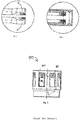
- Figure 1 shows a schematic view of an outer conductor arrangement 100 according to the invention in the unassembled state.
- the outer conductor arrangement 100 according to the invention comprises the outer conductor base body 200 and the outer conductor ring 300.
- the outer conductor arrangement 100 is designed to receive one or more inner conductors and one or more insulating parts in order to provide a coaxial, twin-axial or triaxial plug connector.
- the outer conductor base body 200 comprises a plurality of contact tabs 201 on its top and bottom and on the right and left side each have a retaining tab, which is designed as a contact tab 203.
- the contact tab 203 is slightly larger than the contact tabs 201 and thus also stiffer than the contact tabs 201.
- the outer conductor ring 300 is also formed on the contact tabs 203, which additionally contributes to an increased rigidity of the contact tabs 203 compared to the contact tabs 201.
- the contact tabs 201 each have a contact point 204 in a front end region.
- the contact point is designed as an elevation on the contact lugs 201 and, when plugged in, makes contact with the outer conductor of a mating connector that is plugged into the outer conductor arrangement 100. This ensures electromagnetic shielding on the upper and lower sides of the outer conductor arrangement 100 from inner conductors (not shown) guided in the outer conductor main body 200 by the outer conductor main body 200.
- the contact tabs 203 also each have a contact point 205.
- the contact point 205 is formed on a spring tab 207 in the contact tab 203. This ensures that the outer conductor arrangement 100 also provides electromagnetic shielding on the sides of the outer conductor arrangement.
- outer conductor base body 200 provides a jump in diameter between the contact lugs 201, 203 and the outer conductor ring 300.
- outer conductor ring 300 is connected to the outer conductor base body 200 via a weld seam 209.
- the outer conductor base body 200 and the outer conductor ring 300 can be formed in one piece.
- the outer conductor ring 300 comprises the protective collar 305, which protects the ends of the contact lugs 201 from the action of force from foreign bodies.
Landscapes
- Details Of Connecting Devices For Male And Female Coupling (AREA)
- Coupling Device And Connection With Printed Circuit (AREA)
Description
- Die vorliegende Erfindung betrifft eine Außenleiteranordnung und ein Herstellungsverfahren für eine Außenleiteranordnung.
- Steckverbinder sind beispielsweise durch den Stecker "PosiBand" von Positronic sowohl mit offenem Eintritt (englisch "open entry") als auch mit geschlossenem Eintritt (englisch "closed entry") bekannt.
- Ein Steckverbinder mit einem offenen Eintritt ist in
Figur 3 gezeigt. Derartige Steckverbinder weisen eine interfaceseitige Vorderkante, die nicht umlaufend geschlossen ist, auf. In der Regel sind Unterbrechungen der Vorderkante durch Kontaktlaschen gebildet. Steckverbinder mit offenem Eintritt können Fertigungstoleranzen besser ausgleichen und reduzieren die zum Stecken erforderlichen Steckkräfte. - Ein Steckverbinder mit einem geschlossenen Eintritt ist in
Figur 4 gezeigt. Derartige Steckverbinder weisen eine geschlossene interfaceseitige Vorderkante auf. Kontaktlaschen können von einem Gehäuse umgeben sein. Steckverbinder mit geschlossenem Eintritt verhindern, dass der Steckverbinder durch mechanische Krafteinflüsse, beispielsweise durch einen Steckversuch mit einem falschen Gegensteckverbinder, beschädigt wird. Sie führen auch zu deutlich erhöhten Steckkräften. - Versuche des Standes der Technik zeigen, dass die Optimierung einer der Parameter EMV-Dichtigkeit, Steckkräfte und Stabilität und Impedanzoptimierung eines Steckverbinders im Hochfrequenzbereich einander entgegenstehen. Beispielsweise ist dies in bestehenden Produkten der Anmelderin, Rosenberger Hochfrequenztechnik GmbH & Co. KG, erkennbar. Die Figur 9 zeigt ein solches Produkt.
- In
Figur 5 ist ein Außenleiter 90 eines Hochvolt (HV)-Steckers, der auf Frequenzen im Megahertzbereich ausgelegt ist, dargestellt. Der Außenleiter umfasst einen geschlossenen Eintritt 91 und federnde Kontaktlaschen 92 mit Kontaktpunkten 93, die sich hinter dem geschlossenen Eintritt befinden. Frequenzabhängig treten Resonanzen an dem Außenleiter aufgrund von Kapazitäten zwischen den Steckpartner auf. Zwar treten die vorstehend genannten Nachteile in diesem Frequenzbereich noch nicht auf, allerdings ergibt sich die Notwendigkeit einen Außenleiter, der für einen Stecker in einem höheren Frequenzbereich geeignet ist, bereitzustellen. DieUS 20140364013 A1 und dieDE 202013001452 U1 zeigen eine Außenleiteranordnung für einen Steckverbinder aufweisend einen Außenleitergrundkörper und einen Außenleiterring, wobei der Außenleitergrundkörper mehrere Kontaktlaschen aufweist, wobei sich der Außenleiterring an einem interfaceseitigen Ende des Außenleitergrundkörpers anschließt, an wenigstens einem Anbindungsbereich mittels einer Haltelasche an den Außenleitergrundkörper angebunden ist und von geschlossener Struktur ist, um einen geschlossenen Eintritt der Außenleiteranordnung zu bilden, wobei Kontaktlaschen vorgesehen sind, die nicht an den Außenleiterring angebunden sind. - Dies ist ein Zustand, den es zu verbessern gilt.
- Die
EP 0476848 B1 , die als nächstliegender Stand der Technik angesehen wird, zeigt eine Außenleiteranordnung für einer Steckverbinder aufweisend einen Außenleitergrundkörper und einen Außenleiterring, wobei der Außenleitergrundkörper mehrere Kontaktlaschen aufweist, wobei sich der Außenleiterring an einem interfaceseitigen Ende des Außenleitergrundkörpers anschließt, an wenigstens einem Anbindungsbereich mittels einer Haltelasche an den Außenleitergrundkörper angebunden ist und von geschlossener Struktur ist, um einen geschlossenen Eintritt der Außenleiteranordnung zu bilden, wobei Kontaktlaschen vorgesehen sind, die nicht an den Außenleiterring angebunden sind, wobei zwischen dem Außenleiterring und dem Außenleitergrundkörper ein Durchmessersprung ausgebildet ist, wobei der Durchmesser des Außenleitergrundkörpers größer ist als der Durchmesser des Außenleiterrings. DieEP 3 396 791 A1 ist Stand der Technik nach Art. 54(3) EPÜ. Sie offenbart eine Außenleiteranordnung gemäß Anspruch 1 bis auf das Merkmal, dass der Außenleiterring keine Einbuchtung und keine Ausbuchtung aufweist. - Vor diesem Hintergrund liegt der vorliegenden Erfindung die Aufgabe zugrunde, einen Steckverbinder mit einem geschlossenen Eintritt und verbesserten Impedanzeigenschaften anzugeben.
- Erfindungsgemäß wird diese Aufgabe durch eine Außenleiteranordnung mit den Merkmalen des Patentanspruchs 1 gelöst.
- Die der vorliegenden Erfindung zugrunde liegende Idee besteht darin, Enden von Kontaktlaschen eines Außenleiters so hinter einem Außenleiterring anzuordnen, dass die Kontaktlaschen flexibel verformbar sind, um niedrige Steckkräfte zu gewährleisten, und gleichzeitig einen geschlossenen Eintritt durch einen Außenleiterring zu schaffen.
- Dementsprechend weisen die nicht an den Außenleiterring angebundenen Kontaktlaschen dieselben toleranzausgleichenden Eigenschaften auf, wie die Kontaktlaschen gemäß Figur 7.
- In dieser Patentanmeldung wird unter einem Ring ein umlaufender Gegenstand verstanden. Seine Querschnittsfläche kann unter anderem rund, oval, ellipsenförmig oder dergleichen sein.
- Erfindungsgemäß weist die Außenleiteranordnung zwischen dem Außenleitergrundkörper und dem Außenleiterring einen Durchmessersprung nach innen auf. Durchmessersprünge im Außenleiter ermöglichen eine Anpassung der Impedanz. Erfindungsgemäß ist der Außenleiterring mit dem Außenleitergrundkörper mittels eines Fügeverfahrens, z.B. mittels Schweißen, verbunden.
- Zudem weist der Außenleiterring keine Einbuchtung und keine Ausbuchtung auf.
- Vorteilhafte Ausgestaltungen und Weiterbildungen ergeben sich aus den weiteren Unteransprüchen sowie aus der Beschreibung unter Bezugnahme auf die Figuren der Zeichnung.
- Es versteht sich, dass die voranstehend genannten und die nachstehend noch zu erläuternden Merkmale nicht nur in der jeweils angegebenen Kombination, sondern auch in anderen Kombinationen oder in Alleinstellung verwendbar sind, ohne den Rahmen der vorliegenden Erfindung zu verlassen.
- Erfindungsgemäß ist vorgesehen, dass der Außenleiterring keine Ausbuchtung oder Einbuchtung aufweist.
- Gemäß einer weiter bevorzugten Ausführungsform der Erfindung ist der Außenleiterring eingerichtet, Kontaktlaschen vor mechanischen Krafteinflüssen zu schützen. Dies ist erforderlich, wenn ein Steckverbinder auch aus einer schrägen Richtung steckbar sein soll oder in gestecktem Zustand Krafteinwirkungen aus einer schrägen Richtung ohne Beschädigung des Außenleiters standhalten soll. Gemäß einer Ausführungsform der vorliegenden Erfindung kann dieser Schutz der Kontaktlaschen durch einen geschlossenen Eintritt des Außenleiters gewährleistet werden.
- Diese Ausführungsform der vorliegenden Erfindung löst somit das Problem, Steckkräfte zu reduzieren und gleichzeitig die Stabilität eines Steckverbinders zu erhöhen. Die Optimierung dieser beiden Eigenschaften ist allerdings in der Praxis gegenläufig, d.h. eine gewünschte Steigerung der Stabilität führt zu einer ungewünschten Steigerung der Steckkräfte und andersherum.
- Gemäß einer weiter bevorzugten Ausführungsform der Erfindung ist wenigstens eine Kontaktlasche als Haltelasche, mit welcher der Außenleiterring verbunden ist, ausgebildet. Auf diese Weise kann der Außenleiterring besonders einfach und sicher an dem Außenleitergrundkörper befestigt werden.
- Alternativ ist es auch möglich, den Außenleiterring an einem anderen Teil des Außenleiters zu befestigen. Insbesondere muss die Haltelasche nicht zwingend eine Kontaktlasche sein. Eine Kontaktlasche dient der Kontaktierung eines Gegensteckverbinders, mit welchem ein die Außenleiteranordnung aufweisender Steckverbinder zu verbinden ist.
- Sind Kontaktlaschen lediglich an den Außenleitergrundkörper angebunden, weisen diese federnde Eigenschaften auf. Die Haltelaschen können derart beschaffen sein, dass ihre Steifigkeit größer ist, als die Steifigkeit der nicht angebundenen Kontaktlaschen.
- Ist der Außenleiterring an mehreren Laschen, insbesondere an zwei Laschen an dem Außenleitergrundkörper angebunden, weist dieser eine geringere Federfähigkeit auf, als die Kontaktlaschen, die nicht an den Außenleiterring angebunden sind.
- Vorteilhaft ist es, wenn eine Haupterstreckungsrichtung der Haltelasche in Umlaufrichtung des Außenleiterhalterings verläuft und/oder wenn die Haupterstreckungsrichtung der Haltelasche senkrecht zu der Haupterstreckungsrichtung der Kontaktlaschen verläuft.
- Besonders vorteilhaft an dem erfindungsgemäßen Steckverbinder ist, dass dieser auch durch ein Stanzverfahren samt der Durchmessersprünge fertigbar ist.
- Wird ein erfindungsgemäßer Steckverbinder durch ein Stanzverfahren gefertigt, können Durchmessersprünge der Haltelaschen erzeugt werden.
- Gemäß einer weiter bevorzugten Ausführungsform der Erfindung weist der Außenleitergrundkörper zwei Haltelaschen auf. Die Haltelaschen können gerade oder gebogen sein.
- Dabei ist es weiter zweckmäßig, wenn in der Haltelasche eine federnde Kontaktlasche vorgesehen ist.
- Gemäß einer bevorzugten Ausführungsform weist der Außenleiterring einen Schutzkragen, welcher in radialer Richtung gegenüber freien Enden der Kontaktlaschen hervorsteht, auf, wobei der Schutzkragen eingerichtet ist, die Kontaktlaschen des Außenleitergrundkörpers vor mechanischen Krafteinwirkungen zu schützen. Dabei kann vorgesehen sein, dass der Schutzkragen verhindert, dass die Kontaktlaschen durch eintretende Gegenstände, beispielsweise Werkzeuge, beschädigt werden. Der Schutzkragen kann in einer Ausführungsform als senkrechte Wandung, die von dem Außenleiterring absteht, ausgebildet sein oder als gebogene Lasche, welche die vorderen Enden der Kontaktlaschen verdeckt.
- Gemäß einer weiter bevorzugten Ausführungsform weisen die Kontaktlaschen jeweils einen erhöhten Kontaktpunkt zur Kontaktierung eines Gegensteckverbinders auf. Somit erfahren die Kontaktlaschen in gestecktem Zustand eine Vorspannung, wodurch sich der Kontakt verbessert. Auf diese Weise wird die Schirmung des Steckverbinders verbessert. Um Steckkräfte zu reduzieren, ist es möglich, diese Kontaktpunkte in axialer Richtung versetzt anzuordnen.
- Gemäß einer nicht beanspruchten Ausführungsform sind der Außenleiterring und der Außenleitergrundkörper einteilig ausgebildet.
- Gemäß einer bevorzugten Ausführungsform der Erfindung ist der Außenleitergrundkörper als Stanzteil ausgebildet. Stanzteile sind auf besonders kostengünstige Weise herstellbar. Insbesondere kann die Produktion von Stanzteilen hochautomatisiert erfolgen. Allerdings ist das Erzeugen von Durchmessersprüngen in Stanzverfahren für Steckverbinder mit einem geschlossenen Eintritt nur in Verbindung mit anderen mechanischen Nachteilen wie hohen Steckkräften oder niedrigen Kontaktkräften möglich.
- Die obigen Ausgestaltungen und Weiterbildungen lassen sich, sofern sinnvoll, beliebig miteinander kombinieren. Weitere mögliche Ausgestaltungen, Weiterbildungen und Implementierungen der Erfindung umfassen auch nicht explizit genannte Kombinationen von zuvor oder im Folgenden bezüglich der Ausführungsbeispiele beschriebenen Merkmale der Erfindung. Insbesondere wird dabei der Fachmann auch Einzelaspekte als Verbesserungen oder Ergänzungen zu der jeweiligen Grundform der vorliegenden Erfindung hinzufügen.
- Die vorliegende Erfindung wird nachfolgend anhand der in den schematischen Figuren der Zeichnung angegebenen Ausführungsbeispiele näher erläutert. Es zeigen dabei:
- Fig. 1
- zeigt eine schematische Perspektivansicht einer Außenleiteranordnung gemäß einer Ausführungsform der Erfindung;
- Fig. 2
- zeigt eine schematische Perspektivansicht einer Außenleiteranordnung gemäß einer Ausführungsform der Erfindung;
- Fig. 3
- zeigt eine schematische Ansicht des Standes der Technik;
- Fig. 4
- zeigt eine schematische Ansicht des Standes der Technik;
- Fig. 5
- zeigt eine schematische Ansicht des Standes der Technik;
- Die beiliegenden Figuren der Zeichnung sollen ein weiteres Verständnis der Ausführungsformen der Erfindung vermitteln. Sie veranschaulichen Ausführungsformen und dienen im Zusammenhang mit der Beschreibung der Erklärung von Prinzipien und Konzepten der Erfindung. Andere Ausführungsformen und viele der genannten Vorteile ergeben sich im Hinblick auf die Zeichnungen. Die Elemente der Zeichnungen sind nicht notwendigerweise maßstabsgetreu zueinander gezeigt.
- In den Figuren der Zeichnung sind gleiche, funktionsgleiche und gleich wirkende Elemente, Merkmale und Komponenten - sofern nichts anderes ausgeführt ist - jeweils mit denselben Bezugszeichen versehen.
- Im Folgenden werden die Figuren zusammenhängend und übergreifend beschrieben.
-
Figur 1 zeigt eine schematische Ansicht einer erfindungsgemäßen Außenleiteranordnung 100 in nicht montierten Zustand. Die erfindungsgemäße Außenleiteranordnung 100 umfasst den Außenleitergrundkörper 200 sowie den Außenleiterring 300. Die Außenleiteranordnung 100 ist dazu ausgebildet ein oder mehrere Innenleiter und ein oder mehrere Isolierteile aufzunehmen, um einen koaxialen, twinaxialen oder triaxialen Steckverbinder bereitzustellen. - Der Außenleitergrundkörper 200 umfasst auf dessen Oberseite und Unterseite mehrere Kontaktlaschen 201 und auf der rechten und linken Seite jeweils eine Haltelasche, welche als Kontaktlasche 203 ausgebildet ist. Die Kontaktlasche 203 ist etwas größer als die Kontaktlaschen 201 und somit auch steifer als die Kontaktlaschen 201. An den Kontaktlaschen 203 ist zudem der Außenleiterring 300 angeformt, der zusätzlich zu einer gesteigerten Steifigkeit der Kontaktlaschen 203 gegenüber der Kontaktlaschen 201 beitragen.
- Die Kontaktlaschen 201 weisen in einem vorderen Endbereich jeweils einen Kontaktpunkt 204 auf. Der Kontaktpunkt ist als Erhöhung auf den Kontaktlaschen 201 ausgebildet und kontaktiert in gestecktem Zustand den Außenleiter eines Gegensteckverbinders, der mit Außenleiteranordnung 100 gesteckt ist. Dies gewährleistet eine elektromagnetische Schirmung an der Ober- und Unterseite der Außenleiteranordnung 100 von in dem Außenleitergrundkörper 200 geführten Innenleitern (nicht dargestellt) durch den Außenleitergrundkörper 200.
- In
Figur 2 weisen auch die Kontaktlaschen 203 jeweils einen Kontaktpunkt 205 auf. Der Kontaktpunkt 205 ist auf einer Federlasche 207 in der Kontaktlasche 203 ausgebildet. Auf diese Weise ist gewährleistet, dass die Außenleiteranordnung 100 auch eine elektromagnetische Schirmung an den Seiten der Außenleiteranordnung bereitstellt. - In
Figur 1 ist zu erkennen, dass der Außenleitergrundkörper 200 einen Durchmessersprung zwischen den Kontaktlaschen 201, 203 und dem Außenleiterring 300 bereitstellt. - In
Figur 1 ist der Außenleiterring 300 mit dem Außenleitergrundkörper 200 über eine Schweißnaht 209 verbunden. Gemäß einer nicht beanspruchten Alternative können der Außenleitergrundkörper 200 und der Außenleiterring 300 einteilig ausgebildet sein. - Der Außenleiterring 300 umfasst den Schutzkragen 305, der die Enden der Kontaktlaschen 201 vor Krafteinwirkung durch Fremdkörper schützt.
-
- 100
- Außenleiteranordnung
- 200
- Außenleitergrundkörper
- 201
- Kontaktlaschen
- 203
- Kontaktlaschen
- 204
- Kontaktpunkt
- 205
- Kontaktpunkt
- 207
- Federlasche
- 300
- Außenleiterring
- 305
- Schutzkragen
Claims (10)
- Außenleiteranordnung (100) für einen Steckverbinder aufweisend einen Außenleitergrundkörper (200) und einen Außenleiterring (300), wobei der Außenleitergrundkörper (200) mehrere Kontaktlaschen (201, 203) aufweist,
wobei sich der Außenleiterring (300) an einem interfaceseitigen Ende des Außenleitergrundkörpers (200) anschließt, an wenigstens einem Anbindungsbereich mittels einer Haltelasche (203) an den Außenleitergrundkörper (200) angebunden ist und von geschlossener Struktur ist, um einen geschlossenen Eintritt der Außenleiteranordnung (100) zu bilden, wobei Kontaktlaschen (201) vorgesehen sind, die nicht an den Außenleiterring (300) angebunden sind, wobei zwischen dem Außenleiterring (300) und dem Außenleitergrundkörper (200) ein Durchmessersprung ausgebildet ist, wobei der Durchmesser des Außenleitergrundkörpers (200) größer ist als der Durchmesser des Außenleiterrings (300), wobei der Außenleiterring (300) keine Einbuchtung und keine Ausbuchtung aufweist, dadurch gekennzeichnet, dass der Außenleiterring (300) mit dem Außenleitergrundkörper (200) mittels eines Fügeverfahrens verbunden ist. - Außenleiteranordnung (100) nach Anspruch 1, wobei der Außenleiterring (300) eingerichtet ist, die Kontaktlaschen (201, 203) vor mechani-schen Krafteinflüssen zu schützen.
- Außenleiteranordnung (100) nach einem der vorstehenden Ansprüche, wobei wenigstens eine Kontaktlasche (203) einen Anbindungsbereich aufweist, indem die Kontaktlasche (203) als Haltelasche (203) ausgebildet ist, an welcher der Außenleiterring (300) angebunden ist.
- Außenleiteranordnung (100) nach Anspruch 3, wobei der Außenleiterring (300) mit der Haltelasche (203) mittels eines Fügeverfahrens, insbesondere mittels einer Schweißnaht verbunden ist.
- Außenleiteranordnung (100) nach Anspruch 3 oder 4, wobei der Außenleitergrundkörper (200) mehrere Haltelaschen (203), insbesondere zwei Haltelaschen (203), aufweist.
- Außenleiteranordnung (100) nach einem der Ansprüche 3-5, wobei die Haltelasche (203) eine federnde Kontaktlasche (207) in der Haltelasche (203) aufweist.
- Außenleiteranordnung (100) nach einem der vorstehenden Ansprüche, wobei der Außenleiterring (300) einen Schutzkragen (305), welcher in radialer Richtung gegenüber freien Enden der Kontaktlaschen (201) hervorsteht, aufweist, wobei der Schutzkrager (305) eingerichtet ist, die Kontaktlaschen (201) des Außenleitergrundkörpers (200) vor mechanischer Krafteinwirkung zu schützen.
- Außenleiteranordnung (100) nach einem der vorstehenden An-sprüche, wobei die Kontaktlaschen (201, 203) jeweils einen erhöhten Kontaktpunkt (204, 205) zur Kontaktierung eines mit dem Steckverbinder zu verbindenden Gegensteckverbinders aufweist.
- Außenleiteranordnung (100) nach Anspruch 8, wobei die Kontaktpunkte (204, 205) zueinander in axialer Richtung des Außenleitergrundkörpers (200) versetzt ausgebildet sind.
- Außenleiteranordnung (100) nach einem der vorstehenden Ansprüche, wobei der Außenleitergrundkörper (200) und/oder der Außenleiterring (300) als Stanzteil ausgebildet sind.
Priority Applications (1)
| Application Number | Priority Date | Filing Date | Title |
|---|---|---|---|
| EP21182088.1A EP3907830B1 (de) | 2018-03-15 | 2019-03-04 | Aussenleiteranordnung |
Applications Claiming Priority (2)
| Application Number | Priority Date | Filing Date | Title |
|---|---|---|---|
| DE102018106004 | 2018-03-15 | ||
| DE102019104754.4A DE102019104754A1 (de) | 2018-03-15 | 2019-02-25 | Außenleiteranordnung |
Related Child Applications (1)
| Application Number | Title | Priority Date | Filing Date |
|---|---|---|---|
| EP21182088.1A Division EP3907830B1 (de) | 2018-03-15 | 2019-03-04 | Aussenleiteranordnung |
Publications (2)
| Publication Number | Publication Date |
|---|---|
| EP3540865A1 EP3540865A1 (de) | 2019-09-18 |
| EP3540865B1 true EP3540865B1 (de) | 2021-07-14 |
Family
ID=65685241
Family Applications (2)
| Application Number | Title | Priority Date | Filing Date |
|---|---|---|---|
| EP19160510.4A Active EP3540865B1 (de) | 2018-03-15 | 2019-03-04 | Aussenleiteranordnung |
| EP21182088.1A Active EP3907830B1 (de) | 2018-03-15 | 2019-03-04 | Aussenleiteranordnung |
Family Applications After (1)
| Application Number | Title | Priority Date | Filing Date |
|---|---|---|---|
| EP21182088.1A Active EP3907830B1 (de) | 2018-03-15 | 2019-03-04 | Aussenleiteranordnung |
Country Status (2)
| Country | Link |
|---|---|
| EP (2) | EP3540865B1 (de) |
| CN (1) | CN114649704B (de) |
Families Citing this family (5)
| Publication number | Priority date | Publication date | Assignee | Title |
|---|---|---|---|---|
| US12170424B2 (en) * | 2021-08-11 | 2024-12-17 | Te Connectivity Germany Gmbh | Contact of an electrical connector with protection tabs for cantilever beams |
| WO2023034396A1 (en) | 2021-09-01 | 2023-03-09 | Fci Usa Llc | High speed, ruggedized connector |
| FR3131111B1 (fr) * | 2021-12-22 | 2024-11-22 | Aptiv Tech Ltd | Ensemble de connexion blindé, connecteur pour cet ensemble de connexion et procédé de fabrication d’un élément de blindage pour cet ensemble de connexion |
| CN115133351B (zh) * | 2022-06-22 | 2025-02-14 | 中航光电科技股份有限公司 | 一种射频同轴连接器及其屏蔽套筒 |
| CN219350728U (zh) * | 2022-12-26 | 2023-07-14 | 长春捷翼汽车科技股份有限公司 | 一种外导体结构 |
Family Cites Families (12)
| Publication number | Priority date | Publication date | Assignee | Title |
|---|---|---|---|---|
| EP0476848B1 (de) * | 1990-09-07 | 1995-12-13 | ITT INDUSTRIES, INC. (a Delaware corporation) | Zusammensetzung einer Steckdosekontakt mit enger Zugang |
| DE4312641C2 (de) | 1993-04-19 | 1995-10-12 | Grote & Hartmann | Elektrische Kontakthülse |
| EP0844699A3 (de) * | 1996-11-26 | 1999-07-28 | Siemens Aktiengesellschaft | Koaxial-Steckverbinderelement |
| CA2272458C (en) * | 1998-06-25 | 2008-03-18 | Leslie Laszlo Kerek | Hoodless electrical socket connector |
| DE102006006845B3 (de) * | 2006-02-15 | 2007-07-19 | Tyco Electronics Amp Gmbh | Elektrische Außenleiterhülse für einen koaxialen Steckverbinder |
| DE202013001452U1 (de) | 2013-02-14 | 2013-03-21 | Rosenberger Hochfrequenztechnik Gmbh & Co. Kg | Adapter |
| CN104241940A (zh) | 2013-06-08 | 2014-12-24 | 凡甲电子(苏州)有限公司 | 电连接器组合 |
| CN103490200B (zh) * | 2013-09-27 | 2015-07-29 | 苏州华旃航天电器有限公司 | 一种具有冲压接触元件的射频同轴电连接器 |
| CN204424526U (zh) * | 2015-02-13 | 2015-06-24 | 常州市新盛电器有限公司 | 公头单元射频连接器 |
| DE102016109266A1 (de) | 2016-05-06 | 2017-11-09 | Rosenberger Hochfrequenztechnik Gmbh & Co. Kg | Steckverbindungsvorrichtung mit wenigstens einem Steckverbinder |
| DE102016123081B4 (de) | 2016-11-30 | 2018-06-14 | Amphenol-Tuchel Electronics Gmbh | Zylindrische Hochstromkontakt-Steckverbinder-Buchse |
| EP3396791B1 (de) * | 2017-04-24 | 2019-10-02 | Rosenberger Hochfrequenztechnik GmbH & Co. KG | Aussenleiteranordnung |
-
2019
- 2019-03-04 EP EP19160510.4A patent/EP3540865B1/de active Active
- 2019-03-04 EP EP21182088.1A patent/EP3907830B1/de active Active
- 2019-03-12 CN CN202210379986.2A patent/CN114649704B/zh active Active
Non-Patent Citations (1)
| Title |
|---|
| None * |
Also Published As
| Publication number | Publication date |
|---|---|
| EP3540865A1 (de) | 2019-09-18 |
| EP3907830C0 (de) | 2024-02-21 |
| CN114649704B (zh) | 2024-04-30 |
| EP3907830A1 (de) | 2021-11-10 |
| CN114649704A (zh) | 2022-06-21 |
| EP3907830B1 (de) | 2024-02-21 |
Similar Documents
| Publication | Publication Date | Title |
|---|---|---|
| EP3907830B1 (de) | Aussenleiteranordnung | |
| EP3396791B1 (de) | Aussenleiteranordnung | |
| DE112018000673B4 (de) | Abschirmanschluss | |
| DE102019104754A1 (de) | Außenleiteranordnung | |
| EP2950395B1 (de) | Federkranz für eine abschirmung von elektrischen steckverbindern | |
| EP3251174B1 (de) | Steckverbinderanordnung mit kompensationscrimp | |
| DE112018000682B4 (de) | Abschirmanschluss | |
| DE102018104253B4 (de) | Steckverbinderanordnung | |
| DE102012105258A1 (de) | Schirmhülse und Abschirmendelement umfassend eine Schirmhülse | |
| EP3227971B1 (de) | Hf-steckverbindung mit selbstschliessender kontakthülse | |
| DE202008014168U1 (de) | Steckverbindung mit einem Stecker- und einem Buchsenteil und diese aufnehmenden Adaptergehäusen | |
| WO2007107208A1 (de) | Rastbarer radsok-steckverbinder | |
| DE112018005968T5 (de) | Verbinderanschluss und Verbinder | |
| EP3787128B1 (de) | Steckverbindung | |
| EP4010949B1 (de) | Elektrischer steckverbinder | |
| DE102010012525A1 (de) | Koaxialstecker mit Klemmverbindungsanschluss des Innenleiters | |
| EP2425500B1 (de) | Adapterelement zur seriellen datenübertragung in einem fahrzeug | |
| DE102018118405B3 (de) | Steckverbinder sowie Steckverbindung mit einem solchen Steckverbinder | |
| EP2586105A1 (de) | Steckverbinder | |
| EP2697869B1 (de) | Steckverbinder mit einem kontaktelement | |
| DE102016213291A1 (de) | Steckereinsatz mit Positionierelement | |
| DE112006001357T5 (de) | Koaxialverbinder und Anordnung zur Anbringung desselben an einem Verbindergehäuse | |
| DE102012105901B4 (de) | Zugentlastungseinheit für einen elektrischen Steckverbinder | |
| EP3407362B1 (de) | Elektrische steckverbindung | |
| DE102014012910A1 (de) | Hochfrequenz-Steckverbindungseinrichtung, insbesondere Koaxial-Steckverbindungseinrichtung für Antennensteckdosen |
Legal Events
| Date | Code | Title | Description |
|---|---|---|---|
| PUAI | Public reference made under article 153(3) epc to a published international application that has entered the european phase |
Free format text: ORIGINAL CODE: 0009012 |
|
| STAA | Information on the status of an ep patent application or granted ep patent |
Free format text: STATUS: REQUEST FOR EXAMINATION WAS MADE |
|
| 17P | Request for examination filed |
Effective date: 20190304 |
|
| AK | Designated contracting states |
Kind code of ref document: A1 Designated state(s): AL AT BE BG CH CY CZ DE DK EE ES FI FR GB GR HR HU IE IS IT LI LT LU LV MC MK MT NL NO PL PT RO RS SE SI SK SM TR |
|
| AX | Request for extension of the european patent |
Extension state: BA ME |
|
| STAA | Information on the status of an ep patent application or granted ep patent |
Free format text: STATUS: EXAMINATION IS IN PROGRESS |
|
| 17Q | First examination report despatched |
Effective date: 20191008 |
|
| TPAC | Observations filed by third parties |
Free format text: ORIGINAL CODE: EPIDOSNTIPA |
|
| GRAP | Despatch of communication of intention to grant a patent |
Free format text: ORIGINAL CODE: EPIDOSNIGR1 |
|
| STAA | Information on the status of an ep patent application or granted ep patent |
Free format text: STATUS: GRANT OF PATENT IS INTENDED |
|
| INTG | Intention to grant announced |
Effective date: 20210211 |
|
| GRAS | Grant fee paid |
Free format text: ORIGINAL CODE: EPIDOSNIGR3 |
|
| GRAA | (expected) grant |
Free format text: ORIGINAL CODE: 0009210 |
|
| STAA | Information on the status of an ep patent application or granted ep patent |
Free format text: STATUS: THE PATENT HAS BEEN GRANTED |
|
| AK | Designated contracting states |
Kind code of ref document: B1 Designated state(s): AL AT BE BG CH CY CZ DE DK EE ES FI FR GB GR HR HU IE IS IT LI LT LU LV MC MK MT NL NO PL PT RO RS SE SI SK SM TR |
|
| REG | Reference to a national code |
Ref country code: GB Ref legal event code: FG4D Free format text: NOT ENGLISH |
|
| REG | Reference to a national code |
Ref country code: IE Ref legal event code: FG4D Free format text: LANGUAGE OF EP DOCUMENT: GERMAN |
|
| REG | Reference to a national code |
Ref country code: DE Ref legal event code: R096 Ref document number: 502019001799 Country of ref document: DE |
|
| REG | Reference to a national code |
Ref country code: AT Ref legal event code: REF Ref document number: 1411378 Country of ref document: AT Kind code of ref document: T Effective date: 20210815 |
|
| REG | Reference to a national code |
Ref country code: SE Ref legal event code: TRGR |
|
| REG | Reference to a national code |
Ref country code: LT Ref legal event code: MG9D |
|
| REG | Reference to a national code |
Ref country code: NL Ref legal event code: MP Effective date: 20210714 |
|
| PG25 | Lapsed in a contracting state [announced via postgrant information from national office to epo] |
Ref country code: ES Free format text: LAPSE BECAUSE OF FAILURE TO SUBMIT A TRANSLATION OF THE DESCRIPTION OR TO PAY THE FEE WITHIN THE PRESCRIBED TIME-LIMIT Effective date: 20210714 Ref country code: FI Free format text: LAPSE BECAUSE OF FAILURE TO SUBMIT A TRANSLATION OF THE DESCRIPTION OR TO PAY THE FEE WITHIN THE PRESCRIBED TIME-LIMIT Effective date: 20210714 Ref country code: RS Free format text: LAPSE BECAUSE OF FAILURE TO SUBMIT A TRANSLATION OF THE DESCRIPTION OR TO PAY THE FEE WITHIN THE PRESCRIBED TIME-LIMIT Effective date: 20210714 Ref country code: HR Free format text: LAPSE BECAUSE OF FAILURE TO SUBMIT A TRANSLATION OF THE DESCRIPTION OR TO PAY THE FEE WITHIN THE PRESCRIBED TIME-LIMIT Effective date: 20210714 Ref country code: NL Free format text: LAPSE BECAUSE OF FAILURE TO SUBMIT A TRANSLATION OF THE DESCRIPTION OR TO PAY THE FEE WITHIN THE PRESCRIBED TIME-LIMIT Effective date: 20210714 Ref country code: NO Free format text: LAPSE BECAUSE OF FAILURE TO SUBMIT A TRANSLATION OF THE DESCRIPTION OR TO PAY THE FEE WITHIN THE PRESCRIBED TIME-LIMIT Effective date: 20211014 Ref country code: PT Free format text: LAPSE BECAUSE OF FAILURE TO SUBMIT A TRANSLATION OF THE DESCRIPTION OR TO PAY THE FEE WITHIN THE PRESCRIBED TIME-LIMIT Effective date: 20211115 Ref country code: BG Free format text: LAPSE BECAUSE OF FAILURE TO SUBMIT A TRANSLATION OF THE DESCRIPTION OR TO PAY THE FEE WITHIN THE PRESCRIBED TIME-LIMIT Effective date: 20211014 Ref country code: LT Free format text: LAPSE BECAUSE OF FAILURE TO SUBMIT A TRANSLATION OF THE DESCRIPTION OR TO PAY THE FEE WITHIN THE PRESCRIBED TIME-LIMIT Effective date: 20210714 |
|
| PG25 | Lapsed in a contracting state [announced via postgrant information from national office to epo] |
Ref country code: PL Free format text: LAPSE BECAUSE OF FAILURE TO SUBMIT A TRANSLATION OF THE DESCRIPTION OR TO PAY THE FEE WITHIN THE PRESCRIBED TIME-LIMIT Effective date: 20210714 Ref country code: LV Free format text: LAPSE BECAUSE OF FAILURE TO SUBMIT A TRANSLATION OF THE DESCRIPTION OR TO PAY THE FEE WITHIN THE PRESCRIBED TIME-LIMIT Effective date: 20210714 Ref country code: GR Free format text: LAPSE BECAUSE OF FAILURE TO SUBMIT A TRANSLATION OF THE DESCRIPTION OR TO PAY THE FEE WITHIN THE PRESCRIBED TIME-LIMIT Effective date: 20211015 |
|
| REG | Reference to a national code |
Ref country code: DE Ref legal event code: R097 Ref document number: 502019001799 Country of ref document: DE |
|
| PG25 | Lapsed in a contracting state [announced via postgrant information from national office to epo] |
Ref country code: DK Free format text: LAPSE BECAUSE OF FAILURE TO SUBMIT A TRANSLATION OF THE DESCRIPTION OR TO PAY THE FEE WITHIN THE PRESCRIBED TIME-LIMIT Effective date: 20210714 |
|
| PLBE | No opposition filed within time limit |
Free format text: ORIGINAL CODE: 0009261 |
|
| STAA | Information on the status of an ep patent application or granted ep patent |
Free format text: STATUS: NO OPPOSITION FILED WITHIN TIME LIMIT |
|
| PG25 | Lapsed in a contracting state [announced via postgrant information from national office to epo] |
Ref country code: SM Free format text: LAPSE BECAUSE OF FAILURE TO SUBMIT A TRANSLATION OF THE DESCRIPTION OR TO PAY THE FEE WITHIN THE PRESCRIBED TIME-LIMIT Effective date: 20210714 Ref country code: SK Free format text: LAPSE BECAUSE OF FAILURE TO SUBMIT A TRANSLATION OF THE DESCRIPTION OR TO PAY THE FEE WITHIN THE PRESCRIBED TIME-LIMIT Effective date: 20210714 Ref country code: RO Free format text: LAPSE BECAUSE OF FAILURE TO SUBMIT A TRANSLATION OF THE DESCRIPTION OR TO PAY THE FEE WITHIN THE PRESCRIBED TIME-LIMIT Effective date: 20210714 Ref country code: EE Free format text: LAPSE BECAUSE OF FAILURE TO SUBMIT A TRANSLATION OF THE DESCRIPTION OR TO PAY THE FEE WITHIN THE PRESCRIBED TIME-LIMIT Effective date: 20210714 Ref country code: CZ Free format text: LAPSE BECAUSE OF FAILURE TO SUBMIT A TRANSLATION OF THE DESCRIPTION OR TO PAY THE FEE WITHIN THE PRESCRIBED TIME-LIMIT Effective date: 20210714 Ref country code: AL Free format text: LAPSE BECAUSE OF FAILURE TO SUBMIT A TRANSLATION OF THE DESCRIPTION OR TO PAY THE FEE WITHIN THE PRESCRIBED TIME-LIMIT Effective date: 20210714 |
|
| 26N | No opposition filed |
Effective date: 20220419 |
|
| PG25 | Lapsed in a contracting state [announced via postgrant information from national office to epo] |
Ref country code: MC Free format text: LAPSE BECAUSE OF FAILURE TO SUBMIT A TRANSLATION OF THE DESCRIPTION OR TO PAY THE FEE WITHIN THE PRESCRIBED TIME-LIMIT Effective date: 20210714 |
|
| REG | Reference to a national code |
Ref country code: CH Ref legal event code: PL |
|
| REG | Reference to a national code |
Ref country code: BE Ref legal event code: MM Effective date: 20220331 |
|
| PG25 | Lapsed in a contracting state [announced via postgrant information from national office to epo] |
Ref country code: LU Free format text: LAPSE BECAUSE OF NON-PAYMENT OF DUE FEES Effective date: 20220304 Ref country code: LI Free format text: LAPSE BECAUSE OF NON-PAYMENT OF DUE FEES Effective date: 20220331 Ref country code: IE Free format text: LAPSE BECAUSE OF NON-PAYMENT OF DUE FEES Effective date: 20220304 Ref country code: CH Free format text: LAPSE BECAUSE OF NON-PAYMENT OF DUE FEES Effective date: 20220331 |
|
| PG25 | Lapsed in a contracting state [announced via postgrant information from national office to epo] |
Ref country code: BE Free format text: LAPSE BECAUSE OF NON-PAYMENT OF DUE FEES Effective date: 20220331 |
|
| P01 | Opt-out of the competence of the unified patent court (upc) registered |
Effective date: 20230525 |
|
| PG25 | Lapsed in a contracting state [announced via postgrant information from national office to epo] |
Ref country code: MK Free format text: LAPSE BECAUSE OF FAILURE TO SUBMIT A TRANSLATION OF THE DESCRIPTION OR TO PAY THE FEE WITHIN THE PRESCRIBED TIME-LIMIT Effective date: 20210714 Ref country code: CY Free format text: LAPSE BECAUSE OF FAILURE TO SUBMIT A TRANSLATION OF THE DESCRIPTION OR TO PAY THE FEE WITHIN THE PRESCRIBED TIME-LIMIT Effective date: 20210714 |
|
| PG25 | Lapsed in a contracting state [announced via postgrant information from national office to epo] |
Ref country code: HU Free format text: LAPSE BECAUSE OF FAILURE TO SUBMIT A TRANSLATION OF THE DESCRIPTION OR TO PAY THE FEE WITHIN THE PRESCRIBED TIME-LIMIT; INVALID AB INITIO Effective date: 20190304 |
|
| PG25 | Lapsed in a contracting state [announced via postgrant information from national office to epo] |
Ref country code: TR Free format text: LAPSE BECAUSE OF FAILURE TO SUBMIT A TRANSLATION OF THE DESCRIPTION OR TO PAY THE FEE WITHIN THE PRESCRIBED TIME-LIMIT Effective date: 20210714 |
|
| PG25 | Lapsed in a contracting state [announced via postgrant information from national office to epo] |
Ref country code: MT Free format text: LAPSE BECAUSE OF FAILURE TO SUBMIT A TRANSLATION OF THE DESCRIPTION OR TO PAY THE FEE WITHIN THE PRESCRIBED TIME-LIMIT Effective date: 20210714 |
|
| REG | Reference to a national code |
Ref country code: AT Ref legal event code: MM01 Ref document number: 1411378 Country of ref document: AT Kind code of ref document: T Effective date: 20240304 |
|
| PG25 | Lapsed in a contracting state [announced via postgrant information from national office to epo] |
Ref country code: AT Free format text: LAPSE BECAUSE OF NON-PAYMENT OF DUE FEES Effective date: 20240304 |
|
| PGFP | Annual fee paid to national office [announced via postgrant information from national office to epo] |
Ref country code: SE Payment date: 20260323 Year of fee payment: 8 |
|
| PGFP | Annual fee paid to national office [announced via postgrant information from national office to epo] |
Ref country code: GB Payment date: 20260304 Year of fee payment: 8 |
|
| PGFP | Annual fee paid to national office [announced via postgrant information from national office to epo] |
Ref country code: DE Payment date: 20260320 Year of fee payment: 8 |
|
| PGFP | Annual fee paid to national office [announced via postgrant information from national office to epo] |
Ref country code: AT Payment date: 20260410 Year of fee payment: 5 |
|
| PGFP | Annual fee paid to national office [announced via postgrant information from national office to epo] |
Ref country code: IT Payment date: 20260320 Year of fee payment: 8 |
|
| PGFP | Annual fee paid to national office [announced via postgrant information from national office to epo] |
Ref country code: FR Payment date: 20260323 Year of fee payment: 8 |