EP3540877A1 - Module de projection laser, caméra de profondeur et dispositif électronique - Google Patents
Module de projection laser, caméra de profondeur et dispositif électronique Download PDFInfo
- Publication number
- EP3540877A1 EP3540877A1 EP19162315.6A EP19162315A EP3540877A1 EP 3540877 A1 EP3540877 A1 EP 3540877A1 EP 19162315 A EP19162315 A EP 19162315A EP 3540877 A1 EP3540877 A1 EP 3540877A1
- Authority
- EP
- European Patent Office
- Prior art keywords
- laser
- projection module
- laser emitter
- emitter
- substrate
- Prior art date
- Legal status (The legal status is an assumption and is not a legal conclusion. Google has not performed a legal analysis and makes no representation as to the accuracy of the status listed.)
- Granted
Links
Images


Classifications
-
- G—PHYSICS
- G01—MEASURING; TESTING
- G01B—MEASURING LENGTH, THICKNESS OR SIMILAR LINEAR DIMENSIONS; MEASURING ANGLES; MEASURING AREAS; MEASURING IRREGULARITIES OF SURFACES OR CONTOURS
- G01B11/00—Measuring arrangements characterised by the use of optical techniques
- G01B11/22—Measuring arrangements characterised by the use of optical techniques for measuring depth
-
- G—PHYSICS
- G06—COMPUTING OR CALCULATING; COUNTING
- G06T—IMAGE DATA PROCESSING OR GENERATION, IN GENERAL
- G06T7/00—Image analysis
- G06T7/50—Depth or shape recovery
- G06T7/521—Depth or shape recovery from laser ranging, e.g. using interferometry; from the projection of structured light
-
- H—ELECTRICITY
- H01—ELECTRIC ELEMENTS
- H01S—DEVICES USING THE PROCESS OF LIGHT AMPLIFICATION BY STIMULATED EMISSION OF RADIATION [LASER] TO AMPLIFY OR GENERATE LIGHT; DEVICES USING STIMULATED EMISSION OF ELECTROMAGNETIC RADIATION IN WAVE RANGES OTHER THAN OPTICAL
- H01S3/00—Lasers, i.e. devices using stimulated emission of electromagnetic radiation in the infrared, visible or ultraviolet wave range
- H01S3/005—Optical devices external to the laser cavity, specially adapted for lasers, e.g. for homogenisation of the beam or for manipulating laser pulses, e.g. pulse shaping
- H01S3/0085—Modulating the output, i.e. the laser beam is modulated outside the laser cavity
-
- H—ELECTRICITY
- H01—ELECTRIC ELEMENTS
- H01S—DEVICES USING THE PROCESS OF LIGHT AMPLIFICATION BY STIMULATED EMISSION OF RADIATION [LASER] TO AMPLIFY OR GENERATE LIGHT; DEVICES USING STIMULATED EMISSION OF ELECTROMAGNETIC RADIATION IN WAVE RANGES OTHER THAN OPTICAL
- H01S3/00—Lasers, i.e. devices using stimulated emission of electromagnetic radiation in the infrared, visible or ultraviolet wave range
- H01S3/05—Construction or shape of optical resonators; Accommodation of active medium therein; Shape of active medium
- H01S3/08—Construction or shape of optical resonators or components thereof
- H01S3/08004—Construction or shape of optical resonators or components thereof incorporating a dispersive element, e.g. a prism for wavelength selection
- H01S3/08009—Construction or shape of optical resonators or components thereof incorporating a dispersive element, e.g. a prism for wavelength selection using a diffraction grating
-
- H—ELECTRICITY
- H01—ELECTRIC ELEMENTS
- H01S—DEVICES USING THE PROCESS OF LIGHT AMPLIFICATION BY STIMULATED EMISSION OF RADIATION [LASER] TO AMPLIFY OR GENERATE LIGHT; DEVICES USING STIMULATED EMISSION OF ELECTROMAGNETIC RADIATION IN WAVE RANGES OTHER THAN OPTICAL
- H01S3/00—Lasers, i.e. devices using stimulated emission of electromagnetic radiation in the infrared, visible or ultraviolet wave range
- H01S3/10—Controlling the intensity, frequency, phase, polarisation or direction of the emitted radiation, e.g. switching, gating, modulating or demodulating
- H01S3/102—Controlling the intensity, frequency, phase, polarisation or direction of the emitted radiation, e.g. switching, gating, modulating or demodulating by controlling the active medium, e.g. by controlling the processes or apparatus for excitation
- H01S3/1028—Controlling the intensity, frequency, phase, polarisation or direction of the emitted radiation, e.g. switching, gating, modulating or demodulating by controlling the active medium, e.g. by controlling the processes or apparatus for excitation by controlling the temperature
-
- H—ELECTRICITY
- H01—ELECTRIC ELEMENTS
- H01S—DEVICES USING THE PROCESS OF LIGHT AMPLIFICATION BY STIMULATED EMISSION OF RADIATION [LASER] TO AMPLIFY OR GENERATE LIGHT; DEVICES USING STIMULATED EMISSION OF ELECTROMAGNETIC RADIATION IN WAVE RANGES OTHER THAN OPTICAL
- H01S5/00—Semiconductor lasers
- H01S5/02—Structural details or components not essential to laser action
- H01S5/022—Mountings; Housings
- H01S5/023—Mount members, e.g. sub-mount members
-
- H—ELECTRICITY
- H01—ELECTRIC ELEMENTS
- H01S—DEVICES USING THE PROCESS OF LIGHT AMPLIFICATION BY STIMULATED EMISSION OF RADIATION [LASER] TO AMPLIFY OR GENERATE LIGHT; DEVICES USING STIMULATED EMISSION OF ELECTROMAGNETIC RADIATION IN WAVE RANGES OTHER THAN OPTICAL
- H01S5/00—Semiconductor lasers
- H01S5/02—Structural details or components not essential to laser action
- H01S5/022—Mountings; Housings
- H01S5/0233—Mounting configuration of laser chips
-
- H—ELECTRICITY
- H01—ELECTRIC ELEMENTS
- H01S—DEVICES USING THE PROCESS OF LIGHT AMPLIFICATION BY STIMULATED EMISSION OF RADIATION [LASER] TO AMPLIFY OR GENERATE LIGHT; DEVICES USING STIMULATED EMISSION OF ELECTROMAGNETIC RADIATION IN WAVE RANGES OTHER THAN OPTICAL
- H01S5/00—Semiconductor lasers
- H01S5/02—Structural details or components not essential to laser action
- H01S5/022—Mountings; Housings
- H01S5/0235—Method for mounting laser chips
-
- H—ELECTRICITY
- H01—ELECTRIC ELEMENTS
- H01S—DEVICES USING THE PROCESS OF LIGHT AMPLIFICATION BY STIMULATED EMISSION OF RADIATION [LASER] TO AMPLIFY OR GENERATE LIGHT; DEVICES USING STIMULATED EMISSION OF ELECTROMAGNETIC RADIATION IN WAVE RANGES OTHER THAN OPTICAL
- H01S5/00—Semiconductor lasers
- H01S5/06—Arrangements for controlling the laser output parameters, e.g. by operating on the active medium
- H01S5/068—Stabilisation of laser output parameters
- H01S5/06804—Stabilisation of laser output parameters by monitoring an external parameter, e.g. temperature
-
- H—ELECTRICITY
- H04—ELECTRIC COMMUNICATION TECHNIQUE
- H04N—PICTORIAL COMMUNICATION, e.g. TELEVISION
- H04N9/00—Details of colour television systems
- H04N9/12—Picture reproducers
- H04N9/31—Projection devices for colour picture display, e.g. using electronic spatial light modulators [ESLM]
- H04N9/3141—Constructional details thereof
- H04N9/315—Modulator illumination systems
- H04N9/3161—Modulator illumination systems using laser light sources
-
- H—ELECTRICITY
- H01—ELECTRIC ELEMENTS
- H01S—DEVICES USING THE PROCESS OF LIGHT AMPLIFICATION BY STIMULATED EMISSION OF RADIATION [LASER] TO AMPLIFY OR GENERATE LIGHT; DEVICES USING STIMULATED EMISSION OF ELECTROMAGNETIC RADIATION IN WAVE RANGES OTHER THAN OPTICAL
- H01S5/00—Semiconductor lasers
- H01S5/02—Structural details or components not essential to laser action
- H01S5/022—Mountings; Housings
- H01S5/023—Mount members, e.g. sub-mount members
- H01S5/02325—Mechanically integrated components on mount members or optical micro-benches
Definitions
- the present disclosure relates to a field of imaging technology, and more particularly, to a laser projection module, a depth camera and an electronic device.
- the laser emitter generates heat when it is in operation, and an excessive temperature of the laser emitter will cause a high temperature drift thereof, thereby affecting the performance of the laser emitter.
- Embodiments of present disclosure provide a laser projection module, a depth camera and an electronic device.
- the laser projection module includes a laser emitter, a collimation element, a diffractive optical element and a temperature detection element.
- the laser emitter is configured to emit laser.
- the collimation element is arranged in a laser emission direction of the laser emitter and configured to collimate the laser.
- the diffractive optical element is arranged in a position subsequent to the collimation element along the laser emission direction of the laser emitter, and configured to diffract the laser collimated by the collimation element to form a laser pattern.
- the temperature detection element is arranged adjacent to the laser emitter and configured to detect a temperature of the laser emitter.
- the temperature detection element is arranged adjacent to the laser emitter, and the temperature detection element may detect the temperature of the laser emitter, such that when the temperature of the laser emitter is too high, the power of the laser emitter is reduced, and thus the problem of affecting the performance of the laser emitter due to the large temperature drift caused by the excessive temperature of the laser emitter can be avoided.
- the laser projection module further includes a substrate assembly, the substrate assembly includes a substrate and a circuit board carried on the substrate, and the laser emitter is carried on the substrate assembly.
- the circuit board is provided with a via hole, both the laser emitter and the temperature detection element are carried on the substrate and received in the via hole.
- the temperature detection element is configured as a thermistor arranged adjacent to the laser emitter.
- the circuit board is provided with a via hole
- the laser emitter is carried on the substrate and received in the via hole
- the substrate is provided with a through hole
- a position of the through hole is opposite to a position where the laser emitter is carried on the substrate
- the temperature detection element is received in the through hole.
- the via hole is aligned with the through hole, and the via hole has a larger section area than the through hole.
- the laser emitter is an edge-emitting laser
- the edge-emitting laser includes a light-emitting surface facing the collimation element.
- the laser projection module further includes a fixing member, and the fixing member is configured to fix the edge-emitting laser to the substrate assembly.
- the fixing member includes a sealant disposed between the edge-emitting laser and the substrate assembly, and the sealant is a thermal conductive adhesive.
- the edge-emitting laser includes: a first end surface facing away from the substrate assembly and configured as the light-emitting surface; a second end surface opposite to the first end surface; and side surfaces extending from the first end surface to the second end surface.
- the sealant is disposed between the second end surface of the edge-emitting laser and the substrate assembly.
- the sealant wraps at least one of the side surfaces of the edge-emitting laser.
- the fixing member includes at least two elastic support members disposed on the substrate assembly, the at least two support members together define a receiving chamber for receiving the laser emitter therein, and the at least two support members are configured to support the laser emitter.
- the depth camera includes a laser projection module according to any one of the above embodiments, an image collector and a processor.
- the temperature detection element is further configured to output a temperature detection signal according to the temperature of the laser emitter.
- the image collector is configured to acquire the laser pattern projected by the laser projection module to a target space.
- the processor is coupled to the temperature detection element, and configured to adjust an emission power of the laser emitter according to the temperature detection signal and to process the laser pattern to obtain a depth image.
- the electronic device includes a housing and a depth camera according to the above embodiment.
- the depth camera is disposed in the housing and configured to be exposed out of the housing to acquire a depth image.
- first and second are used herein for purposes of description and are not intended to indicate or imply relative importance or significance.
- the feature defined with “first” and “second” may comprise one or more this feature.
- a plurality of means two or more than two, unless specified otherwise.
- the terms “mounted,” “connected,” “coupled,” “fixed” and the like are used broadly, and may be, for example, fixed connections, detachable connections, or integral connections; may also be mechanical or electrical connections; may also be direct connections or indirect connections via intervening structures; may also be inner communications of two elements, which can be understood by those skilled in the art according to specific situations.
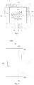
- the laser projection module 100 includes a laser emitter 10, a collimation element 20, a diffractive optical element 30 and a temperature detection element 50.
- the laser emitter 10 is configured to emit laser.
- the collimation element 20 is configured to collimate the laser.
- the diffractive optical element 30 is configured to diffract the laser collimated by the collimation element 20 to form a laser pattern.
- the temperature detection element 50 is configured to detect a temperature of the laser emitter 10 and output a temperature detection signal.
- the laser projection module 100 further includes a substrate assembly 60.
- the substrate assembly 60 includes a substrate 62 and a circuit board 61 carried on the substrate 62.
- the laser emitter 10 is carried on the substrate assembly 60.
- the circuit board 61 is provided with a via hole 611. Both the laser emitter 10 and the temperature detection element 50 are carried on the substrate 62 and received in the via hole 611.
- the circuit board 61 is provided with a via hole 611.
- the laser emitter 10 is carried on the substrate 62 and received in the via hole 611.
- the substrate 62 is provided with a through hole 621, and the position of the through hole 621 is opposite to a position where the laser emitter 10 is carried on the substrate 62.
- the temperature detection element 50 is received in the through hole 621.
- the via hole 611 is aligned with the through hole 621, and the via hole 611 has a larger section area than the through hole 621, such that the laser emitter 10 can be supported on the substrate 62, and also, the temperature detection element 50 can be arranged adjacent to the laser emitter 10, thus facilitating the temperature detection of the laser emitter 10.
- the laser emitter 10 is an edge-emitting laser.
- the edge-emitting laser 10 includes a light-emitting surface 11 that faces the collimation element 20.
- the laser projection module 100 further includes a fixing member.
- the fixing member is configured to fix the edge-emitting laser to the substrate assembly 60.
- the fixing member includes a sealant 15 disposed between the edge-emitting laser and the circuit board 61.
- the sealant 15 is a thermal conductive adhesive.
- the fixing member includes at least two elastic support members 16 disposed on the substrate assembly 60, and the at least two support members 16 together define a receiving chamber.
- the receiving chamber is configured for receiving the laser emitter 10 therein.
- the at least two support members 16 are configured to support the laser emitter 10.
- inventions of the present disclosure also provide a depth camera 1000.
- the depth camera 1000 includes a laser projection module 100 according to any one of the above embodiments, an image collector 200 and a processor 80.
- the image collector 200 is configured to capture the laser pattern projected by the laser projection module 100 to a target space.
- the processor 80 is coupled to the temperature detection element 50.
- the processor 80 is configured to adjust an emission power of the laser emitter 10 according to the temperature detection signal and to process the laser pattern to obtain a depth image.
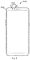
- inventions of the present disclosure further provide an electronic device 3000.
- the electronic device 3000 includes a housing 2000 and a depth camera 1000 according to the above embodiments.
- the depth camera 1000 is disposed in the housing 2000 and configured to be exposed out of the housing 2000 to obtain a depth image.
- the laser projection module 100 includes a lens barrel 40 and a substrate assembly 60.
- the substrate assembly 60 includes a substrate 62 and a circuit board 61.
- the circuit board 61 is carried on the substrate 62.
- the lens barrel 40 includes a side wall 41 and a bearing stage 411 extending from the side wall 41.
- the side wall 41 is disposed on the circuit board 61, and the side wall 41 and the circuit board 61 together define an accommodating cavity 42.
- the laser projection module 100 further includes a laser emitter 10, a collimation element 20, a diffractive optical element 30 and a temperature detection element 50.
- the laser emitter 10, the collimation element 20, the diffractive optical element 30 and the temperature detection element 50 are all received in the accommodating cavity 42, and the collimation element 20 and the diffractive optical element 30 are arranged in sequence along a laser emission direction of the laser emitter 10.
- the circuit board 61 is provided with a via hole 611, and the laser emitter 10 is carried on the substrate 62 and received in the via hole 611.
- the laser emitter 10 is configured to emit laser.
- the collimation element 20 is configured to collimate the laser emitted by the laser emitter 10.
- the diffractive optical element 30 is placed on the bearing stage 411 for diffracting the laser collimated by the collimation element 20 to form a laser pattern.
- the temperature detection element 50 is received in the via hole 611 together with the laser emitter 10, and the temperature detection element 50 may be a thermistor carried on the substrate 62 and placed adjacent to the laser emitter 10.
- the temperature detection element 50 is configured for detecting a temperature of the laser emitter 10 and outputting a temperature detection signal, and the temperature detection signal may be used as a basis for adjusting the power of the laser emitter 10.
- the laser emitter 10 may generate heat when it is in operation, thus causing the temperature of the laser emitter 10 itself to rise.
- the increase in temperature of the laser emitter 10 will affect the performance of the laser emitter 10. For example, an increase in temperature may cause the laser emitter 10 to produce a temperature drift, that is, a central wavelength of the laser emitter 10 is shifted.
- an optical filtering waveband corresponding to an optical filter of the image collector 200 illustrated in Fig.
- the temperature drift results in a problem that a portion of the laser emitted by the laser emitter 10, whose wavelength exceeds the optical filtering waveband, cannot be collected by the image collector 200. Therefore, the image collector 200 cannot accurately acquire the laser pattern projected by the laser projection module 100, thereby further affecting acquisition of the depth image.
- the temperature detection element 50 is arranged adjacent to the laser emitter 10, and the temperature detection element 50 can detect the temperature of the laser emitter 10, such that when the temperature of the laser emitter 10 is too high, the power of the laser emitter 10 can be reduced.
- the heat generated during the operation of the laser emitter 10 is reduced, the temperature of the laser emitter 10 can be lowered, and further, the problem of affecting the performance of the laser emitter 10 due to the large temperature drift caused by the excessive temperature of the laser emitter 10 can be avoided.
- the laser emitter 10 may be a vertical cavity surface emitting laser (VCSEL), and the vertical cavity surface emitting laser has a laser emission direction facing the collimation element 20. Since the vertical cavity surface emitting laser has a multipoint light source distributed in an irregular array, the laser patterns projected by the laser projection module 100 have relatively high irrelevance, which benefits improvement of the acquisition accuracy of the depth image.
- VCSEL vertical cavity surface emitting laser
- the laser emitter 10 may be an edge-emitting laser (EEL).
- the laser emitter 10 may be a distributed feedback laser (DFB).
- the light-emitting surface 11 of the laser emitter 10 faces the collimation element 20 (as illustrated in Fig. 5 ). Characterized by a low temperature drift and a single-point light-emitting structure, the distributed feedback laser needs no array structure and can be easily produced, and thus the cost of the laser projection module 100 is low.
- the circuit board 61 is provided with a via hole 611, and the laser emitter 10 is carried on the substrate 62 and received in the via hole 611.
- the substrate 62 is provided with a through hole 621, and a position of the through hole 621 is opposite to a position where the laser emitter 10 is carried on the substrate 62.
- the temperature detection element 50 is received in the through hole 621.
- the laser emitter 10 may be the vertical cavity surface emitting laser (As illustrated in Fig. 3 ) or the distributed feedback laser (As illustrated in Fig. 4 ).
- the temperature detection element 50 is closer to a central light-emitting portion of the laser emitter 10, and can more accurately detect the temperature of the laser emitter 10, so that the power of the laser emitter 10 can be adjusted more timely, and the performance of the laser emitter 10 can be optimized.
- the laser emitter 10 is the distributed feedback laser
- the power of the distributed feedback laser needs to be enhanced by increasing the length of the distributed feedback laser.
- the distributed feedback laser is arranged vertically (i.e., the light-emitting surface 11 of the distributed feedback laser faces the collimation element 20), the thickness of the laser projection module 100 is relatively large.
- the temperature detection element 50 can be received in the through hole 621, and the laser emitter 10 can be partially received in the via hole 611, such that the thickness of the laser projection module 100 can be effectively reduced, and the laser projection module 100 can be integrated into an electronic device 3000 (as illustrated in Fig. 9 ) such as a smart phone, a tablet computer, a smart watch or a smart wristband.
- an electronic device 3000 such as a smart phone, a tablet computer, a smart watch or a smart wristband.
- the circuit board 61 in the substrate assembly 60 may be a rigid board, a flexible board or a rigid-flex board.
- the substrate 62 is further provided with a heat dissipation hole 622.
- the heat generated by the operation of the laser emitter 10 or the circuit board 61 can be dissipated through the heat dissipation hole 622.
- the heat dissipation hole 622 may also be filled with the thermal conductive adhesive to further improve the heat dissipation performance of the substrate 62.
- the temperature detection element 50 and the laser emitter 10 are both carried on the substrate 62, the temperature detection element 50 is received in the via hole 611 and arranged adjacent to the laser emitter 10, and the laser emitter 10 is entirely accommodated in the via hole 611 (i.e., the laser emitter 10 is the vertical cavity surface emitting laser).
- the laser emitter 10 is the vertical cavity surface emitting laser.
- a plurality of heat dissipation holes 622 are provided and equidistantly distributed (As illustrated in Fig. 1 ).
- the temperature detection element 50 and the laser emitter 10 are both carried on the substrate 62, the temperature detection element 50 is received in the via hole 611 and arranged adjacent to the laser emitter 10, and the laser emitter 10 is partially received in the via hole 611 (i.e., the laser emitter 10 is the edge-emitting laser).
- a plurality of heat dissipation holes 622 and provided and equidistantly distributed As illustrated in Fig. 2 ).
- the laser emitter 10 is completely received in the via hole 611 (i.e., the laser emitter 10 is the vertical cavity surface emitting laser), and the temperature detection element 50 is arranged in the through hole 621 of the substrate 62.
- a plurality of heat dissipation holes 622 are provided and respectively disposed on both sides of the through hole 621, and the heat dissipation holes 622 located on the same side are evenly distributed (As illustrated in Fig. 3 ).
- the laser emitter 10 is partially received in the via hole 611 (i.e., the laser emitter 10 is the edge-emitting laser), and the temperature detection element 50 is arranged in the through hole 621 of the substrate 62.
- a plurality of heat dissipation holes 622 are provided and respectively disposed on both sides of the through hole 621, and the heat dissipation holes 622 located on the same side are evenly distributed (As illustrated in Fig. 4 ).
- the laser emitter 10 is the edge-emitting laser.
- the laser projection module 100 further includes a fixing member.
- the laser emitter 10 has a columnar shape, and an end surface of the laser emitter 10 facing away from the substrate 62 is configured as a light-emitting surface 11. The laser is emitted from the light-emitting surface 11, and the light-emitting surface 11 faces the collimation element 20.
- the laser emitter 10 is fixed to the substrate 62.
- the fixing member is a sealant 15 and the laser emitter 10 is adhered to the substrate 62 by the sealant 15.
- an end surface of the laser emitter 10 opposite to the light-emitting surface 11 is adhered to the substrate 62.
- a side surface 12 of the laser emitter 10 extending between the two end surfaces thereof may also be adhered to the substrate 62.
- the sealant 15 may wrap the surrounding side surfaces 12. Or, the sealant 15 may adhere only one of the side surfaces 12 to the substrate 62 or several of the side surfaces 12 to the substrate 62. In this case, the sealant 15 may be the thermal conductive adhesive to conduct the heat generated by the operation of the laser emitter 10 to the substrate 62.
- the edge-emitting laser generally has a strip shape, when the light-emitting surface 11 of the edge-emitting laser faces the collimation element 20, the edge-emitting laser is arranged vertically. In this case, the edge-emitting laser is prone to accidents such as dropping, shifting, or shaking, and thus the sealant 15 may be provided to fix the edge-emitting laser so as to prevent accidents such as falling, shifting or shaking of the edge-emitting laser.
- the laser emitter 10 is the edge-emitting laser.
- the laser projection module 100 further includes a fixing member.
- the laser emitter 10 has a columnar shape, and an end surface of the laser emitter 10 facing away from the substrate 62 is configured as a light-emitting surface 11.
- the laser is emitted from the light-emitting surface 11, and the light-emitting surface 11 faces the collimation element 20.
- the laser emitter 10 is fixed to the substrate 62.
- the fixing member includes an elastic support member 16. Two or more support members 16 may be provided.
- the support members 16 together define a receiving chamber 161.
- the receiving chamber 161 is configured for receiving the laser emitter 10 therein, and the support members 16 are configured for supporting the laser emitter 10. In this way, it is possible to prevent the laser emitter 10 from being shaken.
- embodiments of the present disclosure also provide a depth camera 1000.
- the depth camera 1000 according to the embodiments of the present disclosure includes a laser projection module 100 according to any one of the above embodiments, an image collector 200 and a processor 80.
- the image collector 200 is configured to collect the laser pattern projected to the target space after being diffracted by the diffractive optical element 30.
- the processor 80 is coupled to the laser projection module 100, the image collector 200 and the temperature detection element 50, respectively.
- the processor 80 is configured to adjust the emission power of the laser emitter 10 according to the temperature detection signal, and to process the laser pattern to acquire a depth image.
- the laser projection module 100 projects the laser pattern to the target space through a projection window 901
- the image collector 200 collects the laser pattern modulated by a target object through an acquisition window 902.
- the image collector 200 may be an infrared camera.
- the processor 80 calculates a deviation value between each pixel point in the laser pattern and a corresponding pixel point in a reference pattern with an image matching algorithm, and then obtains the depth image of the laser pattern based on the deviation value.
- the image matching algorithm may be a digital image correlation (DIC) algorithm. Certainly, other image matching algorithms may be adopted to replace the DIC algorithm.
- the temperature detection element 50 is arranged adjacent to the laser emitter 10, and the temperature detection element 50 may detect the temperature of the laser emitter 10, such that when the temperature of the laser emitter 10 is too high, the power of the laser emitter 10 is reduced, and thus the problem of affecting the performance of the laser emitter 10 due to the large temperature drift caused by the excessive temperature of the laser emitter 10 can be avoided.
- an electronic device 3000 includes a housing 2000 and a depth camera 1000 according to the above embodiments.
- the depth camera 1000 is disposed in the housing 2000 and configured to be exposed out of the housing 2000 to obtain a depth image.
- the temperature detection element 50 is arranged adjacent to the laser emitter 10, and the temperature detection element 50 can detect the temperature of the laser emitter 10, such that when the temperature of the laser emitter 10 is too high, the power of the laser emitter 10 is reduced.
- the heat generated during the operation of the laser emitter 10 is reduced, the temperature of the laser emitter 10 can be lowered, and further, the problem of affecting the performance of the laser emitter 10 due to the large temperature drift caused by the excessive temperature of the laser emitter 10 can be avoided.
Landscapes
- Physics & Mathematics (AREA)
- Optics & Photonics (AREA)
- Electromagnetism (AREA)
- General Physics & Mathematics (AREA)
- Condensed Matter Physics & Semiconductors (AREA)
- Engineering & Computer Science (AREA)
- Plasma & Fusion (AREA)
- Multimedia (AREA)
- Signal Processing (AREA)
- Theoretical Computer Science (AREA)
- Computer Vision & Pattern Recognition (AREA)
- Semiconductor Lasers (AREA)
- Studio Devices (AREA)
- Laser Beam Processing (AREA)
- Measurement Of Optical Distance (AREA)
Applications Claiming Priority (1)
| Application Number | Priority Date | Filing Date | Title |
|---|---|---|---|
| CN201810201174.2A CN108344376A (zh) | 2018-03-12 | 2018-03-12 | 激光投射模组、深度相机和电子装置 |
Publications (2)
| Publication Number | Publication Date |
|---|---|
| EP3540877A1 true EP3540877A1 (fr) | 2019-09-18 |
| EP3540877B1 EP3540877B1 (fr) | 2022-12-21 |
Family
ID=62956564
Family Applications (1)
| Application Number | Title | Priority Date | Filing Date |
|---|---|---|---|
| EP19162315.6A Active EP3540877B1 (fr) | 2018-03-12 | 2019-03-12 | Module de projection laser, caméra de profondeur et dispositif électronique |
Country Status (6)
| Country | Link |
|---|---|
| US (1) | US11082671B2 (fr) |
| EP (1) | EP3540877B1 (fr) |
| CN (1) | CN108344376A (fr) |
| ES (1) | ES2936475T3 (fr) |
| TW (1) | TW201939113A (fr) |
| WO (1) | WO2019174382A1 (fr) |
Families Citing this family (19)
| Publication number | Priority date | Publication date | Assignee | Title |
|---|---|---|---|---|
| CN109242901B (zh) * | 2017-07-11 | 2021-10-22 | 深圳市道通智能航空技术股份有限公司 | 应用于三维相机的图像校准方法和装置 |
| CN108344376A (zh) | 2018-03-12 | 2018-07-31 | 广东欧珀移动通信有限公司 | 激光投射模组、深度相机和电子装置 |
| CN110278426B (zh) * | 2018-03-18 | 2024-02-13 | 宁波舜宇光电信息有限公司 | 深度信息摄像模组及其基座组件、电子设备和制备方法 |
| CN110687688B (zh) * | 2018-07-04 | 2021-12-31 | 三赢科技(深圳)有限公司 | 光学投射装置 |
| CN109149355B (zh) * | 2018-09-12 | 2020-06-23 | Oppo广东移动通信有限公司 | 光发射模组及其控制方法、tof深度相机和电子设备 |
| CN109088963B (zh) * | 2018-09-14 | 2020-08-28 | Oppo广东移动通信有限公司 | 电子装置 |
| CN109120837B (zh) * | 2018-10-31 | 2020-05-01 | Oppo广东移动通信有限公司 | 图像获取方法、图像获取装置、结构光组件及电子装置 |
| CN111327812B (zh) * | 2018-12-14 | 2022-03-04 | 杭州海康威视数字技术股份有限公司 | 一种摄像机组件及摄像机控制方法 |
| CN111684298A (zh) * | 2019-01-09 | 2020-09-18 | 深圳市大疆创新科技有限公司 | 一种测距装置及移动平台 |
| CN109904718B (zh) * | 2019-03-25 | 2020-09-04 | Oppo广东移动通信有限公司 | 飞行时间组件的控制系统及控制方法、终端 |
| CN110488562A (zh) * | 2019-08-19 | 2019-11-22 | 北京驭光科技发展有限公司 | 集成化激光投射模组 |
| CN110530611B (zh) * | 2019-08-30 | 2021-07-09 | Oppo广东移动通信有限公司 | 校准方法、激光发射模组、深度相机和电子设备 |
| EP4045908A1 (fr) | 2019-10-18 | 2022-08-24 | The Regents Of The University Of California | Modèle d'angiogenèse tumorale ex vivo |
| CN112885939B (zh) * | 2019-11-13 | 2022-12-20 | 北京小米移动软件有限公司 | 封装结构、电子设备的发射装置及电子设备 |
| CN111596507B (zh) * | 2020-05-11 | 2022-04-22 | 常州纵慧芯光半导体科技有限公司 | 一种摄像模组及其制造方法 |
| CN115550523A (zh) * | 2021-06-29 | 2022-12-30 | 北京小米移动软件有限公司 | 激光发射模块、深度相机及电子设备 |
| CN113763485B (zh) * | 2021-09-28 | 2022-07-26 | 合肥的卢深视科技有限公司 | 温漂系数获取方法、电子设备、存储介质和图像校正方法 |
| CN114895477B (zh) * | 2022-04-13 | 2024-03-01 | 嘉兴驭光光电科技有限公司 | 激光投射器、相机组件和电子装置 |
| CN116698366A (zh) * | 2023-05-17 | 2023-09-05 | 武汉锐科光纤激光技术股份有限公司 | 光学元件的温升测试装置 |
Citations (3)
| Publication number | Priority date | Publication date | Assignee | Title |
|---|---|---|---|---|
| EP1689055A1 (fr) * | 2003-11-27 | 2006-08-09 | Sony Corporation | Systeme laser |
| EP2363686A1 (fr) * | 2010-02-02 | 2011-09-07 | Primesense Ltd. | Appareil optique, système d'imagerie et procédé de fabrication d'un module photonique |
| US20140072004A1 (en) * | 2012-09-12 | 2014-03-13 | Innovative Photonic Solutions | Wavelength-Stabilized Diode Laser |
Family Cites Families (26)
| Publication number | Priority date | Publication date | Assignee | Title |
|---|---|---|---|---|
| CN1536563A (zh) | 2000-10-17 | 2004-10-13 | ���µ�����ҵ��ʽ���� | 透镜组、光学头和使用它们的光可记录型播放器 |
| TWI384713B (zh) | 2009-08-18 | 2013-02-01 | Quarton Inc | 雷射模組 |
| TWI403049B (zh) | 2010-05-11 | 2013-07-21 | Ind Tech Res Inst | 雷射光源產生裝置 |
| US9557574B2 (en) | 2010-06-08 | 2017-01-31 | Microsoft Technology Licensing, Llc | Depth illumination and detection optics |
| US8330822B2 (en) * | 2010-06-09 | 2012-12-11 | Microsoft Corporation | Thermally-tuned depth camera light source |
| JP5545144B2 (ja) | 2010-09-14 | 2014-07-09 | セイコーエプソン株式会社 | 光デバイスユニット及び検出装置 |
| CN102955328B (zh) * | 2011-08-26 | 2015-02-18 | 深圳市安星数字系统有限公司 | 激光夜视一体化高速云台摄像机及其监控方法 |
| CN202562445U (zh) * | 2012-03-29 | 2012-11-28 | 中国气象局气象探测中心 | 基于激光测距原理的积雪深度多点自动测量装置 |
| TW201347331A (zh) | 2012-05-03 | 2013-11-16 | Sintai Optical Shenzhen Co Ltd | 雷射裝置的溫控方法及使用其之電子裝置 |
| TW201428925A (zh) | 2013-01-04 | 2014-07-16 | 矽品精密工業股份有限公司 | 光電模組結構 |
| CN203387514U (zh) | 2013-06-24 | 2014-01-08 | 青岛海信宽带多媒体技术有限公司 | 可调节发射波长的光网络单元光模块 |
| US10085013B2 (en) * | 2013-12-24 | 2018-09-25 | Lg Electronics Inc. | 3D camera module |
| US9952036B2 (en) * | 2015-11-06 | 2018-04-24 | Intel Corporation | Systems, methods, and apparatuses for implementing maximum likelihood image binarization in a coded light range camera |
| JP6644563B2 (ja) | 2016-01-28 | 2020-02-12 | 浜松ホトニクス株式会社 | レーザ光照射装置 |
| CN206149421U (zh) * | 2016-08-12 | 2017-05-03 | 北京旷视科技有限公司 | 激光模组功率校准单元及深度相机 |
| CN206412341U (zh) * | 2017-01-19 | 2017-08-15 | 深圳奥比中光科技有限公司 | 芯片嵌入装置 |
| CN206470523U (zh) * | 2017-01-19 | 2017-09-05 | 深圳奥比中光科技有限公司 | 光学投影装置及应用其的深度相机 |
| CN206877030U (zh) | 2017-07-07 | 2018-01-12 | 深圳奥比中光科技有限公司 | 发光装置及其激光投影模组 |
| CN107357118A (zh) * | 2017-08-02 | 2017-11-17 | 深圳奥比中光科技有限公司 | 具有高散热性能的光学模组 |
| CN107609383B (zh) * | 2017-10-26 | 2021-01-26 | 奥比中光科技集团股份有限公司 | 3d人脸身份认证方法与装置 |
| WO2019165885A1 (fr) * | 2018-02-27 | 2019-09-06 | Oppo广东移动通信有限公司 | Module de projection laser et procédé de détection pour sa fissuration, caméra de profondeur et dispositif électronique |
| CN108344376A (zh) * | 2018-03-12 | 2018-07-31 | 广东欧珀移动通信有限公司 | 激光投射模组、深度相机和电子装置 |
| WO2019174436A1 (fr) * | 2018-03-12 | 2019-09-19 | Oppo广东移动通信有限公司 | Procédé de commande, dispositif de commande, caméra de profondeur et dispositif électronique |
| CN108594393A (zh) * | 2018-04-04 | 2018-09-28 | Oppo广东移动通信有限公司 | 衍射光学组件、激光投射模组、深度相机和电子装置 |
| WO2019201010A1 (fr) * | 2018-04-16 | 2019-10-24 | Oppo广东移动通信有限公司 | Projecteur laser, module de caméra et dispositif électronique |
| CN108776391B (zh) * | 2018-06-28 | 2020-04-24 | Oppo广东移动通信有限公司 | 激光投射器、图像获取装置和电子设备 |
-
2018
- 2018-03-12 CN CN201810201174.2A patent/CN108344376A/zh active Pending
-
2019
- 2019-01-08 WO PCT/CN2019/070769 patent/WO2019174382A1/fr not_active Ceased
- 2019-03-07 US US16/295,757 patent/US11082671B2/en active Active
- 2019-03-12 ES ES19162315T patent/ES2936475T3/es active Active
- 2019-03-12 EP EP19162315.6A patent/EP3540877B1/fr active Active
- 2019-03-12 TW TW108108333A patent/TW201939113A/zh unknown
Patent Citations (3)
| Publication number | Priority date | Publication date | Assignee | Title |
|---|---|---|---|---|
| EP1689055A1 (fr) * | 2003-11-27 | 2006-08-09 | Sony Corporation | Systeme laser |
| EP2363686A1 (fr) * | 2010-02-02 | 2011-09-07 | Primesense Ltd. | Appareil optique, système d'imagerie et procédé de fabrication d'un module photonique |
| US20140072004A1 (en) * | 2012-09-12 | 2014-03-13 | Innovative Photonic Solutions | Wavelength-Stabilized Diode Laser |
Also Published As
| Publication number | Publication date |
|---|---|
| ES2936475T3 (es) | 2023-03-17 |
| WO2019174382A1 (fr) | 2019-09-19 |
| CN108344376A (zh) | 2018-07-31 |
| US11082671B2 (en) | 2021-08-03 |
| EP3540877B1 (fr) | 2022-12-21 |
| US20190281265A1 (en) | 2019-09-12 |
| TW201939113A (zh) | 2019-10-01 |
Similar Documents
| Publication | Publication Date | Title |
|---|---|---|
| US11082671B2 (en) | Laser projection module, depth camera and electronic device | |
| EP3550340B1 (fr) | Ensemble optique diffractif, unité de projection laser, caméra de profondeur et dispositif électronique | |
| CN108646425B (zh) | 激光投射器、图像获取装置及电子设备 | |
| CN108388072B (zh) | 激光投射模组、深度相机和电子装置 | |
| US11199398B2 (en) | Laser projection module, depth camera and electronic device | |
| EP3531204B1 (fr) | Module de projection laser, caméra de profondeur et dispositif électronique | |
| CN108415209B (zh) | 结构光投射模组、摄像组件和电子装置 | |
| CN108646426A (zh) | 激光投射模组、图像撷取装置和电子设备 | |
| CN108594458A (zh) | 激光投射器、相机模组及电子设备 | |
| CN108490636A (zh) | 结构光投射器、光电设备及电子装置 | |
| CN108508625A (zh) | 结构光投射器、图像获取装置和电子设备 | |
| CN108490630B (zh) | 激光投射模组、深度相机和电子装置 | |
| CN108388065B (zh) | 结构光投射器、光电设备和电子装置 | |
| CN108490572B (zh) | 激光投射模组、深度相机及电子装置 | |
| HK40010718A (en) | Laser projection module, depth camera and electronic device | |
| CN108490577A (zh) | 结构光投射器、图像获取装置和电子设备 | |
| HK40010718B (en) | Laser projection module, depth camera and electronic device | |
| CN108535828A (zh) | 衍射光学组件、激光投射模组、深度相机及电子装置 | |
| US10962870B2 (en) | Laser projection unit, depth camera and electronic device | |
| CN108490595B (zh) | 结构光投射模组、图像获取装置及电子设备 | |
| HK40008198A (en) | Laser projection module, depth camera, and electronic device | |
| HK40008508A (en) | Laser projection module, depth camera and electronic device | |
| HK40008508B (en) | Laser projection module, depth camera and electronic device | |
| HK40014413B (en) | Diffractive optical assembly, laser projection unit, depth camera and electronic device | |
| HK40014413A (en) | Diffractive optical assembly, laser projection unit, depth camera and electronic device |
Legal Events
| Date | Code | Title | Description |
|---|---|---|---|
| PUAI | Public reference made under article 153(3) epc to a published international application that has entered the european phase |
Free format text: ORIGINAL CODE: 0009012 |
|
| STAA | Information on the status of an ep patent application or granted ep patent |
Free format text: STATUS: THE APPLICATION HAS BEEN PUBLISHED |
|
| AK | Designated contracting states |
Kind code of ref document: A1 Designated state(s): AL AT BE BG CH CY CZ DE DK EE ES FI FR GB GR HR HU IE IS IT LI LT LU LV MC MK MT NL NO PL PT RO RS SE SI SK SM TR |
|
| AX | Request for extension of the european patent |
Extension state: BA ME |
|
| RAP1 | Party data changed (applicant data changed or rights of an application transferred) |
Owner name: GUANGDONG OPPO MOBILE TELECOMMUNICATIONS CORP., LT |
|
| STAA | Information on the status of an ep patent application or granted ep patent |
Free format text: STATUS: REQUEST FOR EXAMINATION WAS MADE |
|
| 17P | Request for examination filed |
Effective date: 20191219 |
|
| RBV | Designated contracting states (corrected) |
Designated state(s): AL AT BE BG CH CY CZ DE DK EE ES FI FR GB GR HR HU IE IS IT LI LT LU LV MC MK MT NL NO PL PT RO RS SE SI SK SM TR |
|
| STAA | Information on the status of an ep patent application or granted ep patent |
Free format text: STATUS: EXAMINATION IS IN PROGRESS |
|
| 17Q | First examination report despatched |
Effective date: 20200602 |
|
| REG | Reference to a national code |
Ref country code: HK Ref legal event code: DE Ref document number: 40010718 Country of ref document: HK |
|
| GRAP | Despatch of communication of intention to grant a patent |
Free format text: ORIGINAL CODE: EPIDOSNIGR1 |
|
| STAA | Information on the status of an ep patent application or granted ep patent |
Free format text: STATUS: GRANT OF PATENT IS INTENDED |
|
| INTG | Intention to grant announced |
Effective date: 20220930 |
|
| GRAS | Grant fee paid |
Free format text: ORIGINAL CODE: EPIDOSNIGR3 |
|
| GRAA | (expected) grant |
Free format text: ORIGINAL CODE: 0009210 |
|
| STAA | Information on the status of an ep patent application or granted ep patent |
Free format text: STATUS: THE PATENT HAS BEEN GRANTED |
|
| AK | Designated contracting states |
Kind code of ref document: B1 Designated state(s): AL AT BE BG CH CY CZ DE DK EE ES FI FR GB GR HR HU IE IS IT LI LT LU LV MC MK MT NL NO PL PT RO RS SE SI SK SM TR |
|
| REG | Reference to a national code |
Ref country code: GB Ref legal event code: FG4D |
|
| REG | Reference to a national code |
Ref country code: DE Ref legal event code: R096 Ref document number: 602019023301 Country of ref document: DE |
|
| REG | Reference to a national code |
Ref country code: CH Ref legal event code: EP |
|
| REG | Reference to a national code |
Ref country code: AT Ref legal event code: REF Ref document number: 1539615 Country of ref document: AT Kind code of ref document: T Effective date: 20230115 |
|
| REG | Reference to a national code |
Ref country code: IE Ref legal event code: FG4D |
|
| REG | Reference to a national code |
Ref country code: NL Ref legal event code: FP |
|
| REG | Reference to a national code |
Ref country code: ES Ref legal event code: FG2A Ref document number: 2936475 Country of ref document: ES Kind code of ref document: T3 Effective date: 20230317 |
|
| REG | Reference to a national code |
Ref country code: LT Ref legal event code: MG9D |
|
| PG25 | Lapsed in a contracting state [announced via postgrant information from national office to epo] |
Ref country code: SE Free format text: LAPSE BECAUSE OF FAILURE TO SUBMIT A TRANSLATION OF THE DESCRIPTION OR TO PAY THE FEE WITHIN THE PRESCRIBED TIME-LIMIT Effective date: 20221221 Ref country code: NO Free format text: LAPSE BECAUSE OF FAILURE TO SUBMIT A TRANSLATION OF THE DESCRIPTION OR TO PAY THE FEE WITHIN THE PRESCRIBED TIME-LIMIT Effective date: 20230321 Ref country code: LT Free format text: LAPSE BECAUSE OF FAILURE TO SUBMIT A TRANSLATION OF THE DESCRIPTION OR TO PAY THE FEE WITHIN THE PRESCRIBED TIME-LIMIT Effective date: 20221221 Ref country code: FI Free format text: LAPSE BECAUSE OF FAILURE TO SUBMIT A TRANSLATION OF THE DESCRIPTION OR TO PAY THE FEE WITHIN THE PRESCRIBED TIME-LIMIT Effective date: 20221221 |
|
| REG | Reference to a national code |
Ref country code: AT Ref legal event code: MK05 Ref document number: 1539615 Country of ref document: AT Kind code of ref document: T Effective date: 20221221 |
|
| PG25 | Lapsed in a contracting state [announced via postgrant information from national office to epo] |
Ref country code: RS Free format text: LAPSE BECAUSE OF FAILURE TO SUBMIT A TRANSLATION OF THE DESCRIPTION OR TO PAY THE FEE WITHIN THE PRESCRIBED TIME-LIMIT Effective date: 20221221 Ref country code: LV Free format text: LAPSE BECAUSE OF FAILURE TO SUBMIT A TRANSLATION OF THE DESCRIPTION OR TO PAY THE FEE WITHIN THE PRESCRIBED TIME-LIMIT Effective date: 20221221 Ref country code: HR Free format text: LAPSE BECAUSE OF FAILURE TO SUBMIT A TRANSLATION OF THE DESCRIPTION OR TO PAY THE FEE WITHIN THE PRESCRIBED TIME-LIMIT Effective date: 20221221 Ref country code: GR Free format text: LAPSE BECAUSE OF FAILURE TO SUBMIT A TRANSLATION OF THE DESCRIPTION OR TO PAY THE FEE WITHIN THE PRESCRIBED TIME-LIMIT Effective date: 20230322 |
|
| P01 | Opt-out of the competence of the unified patent court (upc) registered |
Effective date: 20230412 |
|
| PG25 | Lapsed in a contracting state [announced via postgrant information from national office to epo] |
Ref country code: SM Free format text: LAPSE BECAUSE OF FAILURE TO SUBMIT A TRANSLATION OF THE DESCRIPTION OR TO PAY THE FEE WITHIN THE PRESCRIBED TIME-LIMIT Effective date: 20221221 Ref country code: RO Free format text: LAPSE BECAUSE OF FAILURE TO SUBMIT A TRANSLATION OF THE DESCRIPTION OR TO PAY THE FEE WITHIN THE PRESCRIBED TIME-LIMIT Effective date: 20221221 Ref country code: PT Free format text: LAPSE BECAUSE OF FAILURE TO SUBMIT A TRANSLATION OF THE DESCRIPTION OR TO PAY THE FEE WITHIN THE PRESCRIBED TIME-LIMIT Effective date: 20230421 Ref country code: EE Free format text: LAPSE BECAUSE OF FAILURE TO SUBMIT A TRANSLATION OF THE DESCRIPTION OR TO PAY THE FEE WITHIN THE PRESCRIBED TIME-LIMIT Effective date: 20221221 Ref country code: CZ Free format text: LAPSE BECAUSE OF FAILURE TO SUBMIT A TRANSLATION OF THE DESCRIPTION OR TO PAY THE FEE WITHIN THE PRESCRIBED TIME-LIMIT Effective date: 20221221 Ref country code: AT Free format text: LAPSE BECAUSE OF FAILURE TO SUBMIT A TRANSLATION OF THE DESCRIPTION OR TO PAY THE FEE WITHIN THE PRESCRIBED TIME-LIMIT Effective date: 20221221 |
|
| PG25 | Lapsed in a contracting state [announced via postgrant information from national office to epo] |
Ref country code: SK Free format text: LAPSE BECAUSE OF FAILURE TO SUBMIT A TRANSLATION OF THE DESCRIPTION OR TO PAY THE FEE WITHIN THE PRESCRIBED TIME-LIMIT Effective date: 20221221 Ref country code: PL Free format text: LAPSE BECAUSE OF FAILURE TO SUBMIT A TRANSLATION OF THE DESCRIPTION OR TO PAY THE FEE WITHIN THE PRESCRIBED TIME-LIMIT Effective date: 20221221 Ref country code: IS Free format text: LAPSE BECAUSE OF FAILURE TO SUBMIT A TRANSLATION OF THE DESCRIPTION OR TO PAY THE FEE WITHIN THE PRESCRIBED TIME-LIMIT Effective date: 20230421 Ref country code: AL Free format text: LAPSE BECAUSE OF FAILURE TO SUBMIT A TRANSLATION OF THE DESCRIPTION OR TO PAY THE FEE WITHIN THE PRESCRIBED TIME-LIMIT Effective date: 20221221 |
|
| REG | Reference to a national code |
Ref country code: DE Ref legal event code: R097 Ref document number: 602019023301 Country of ref document: DE |
|
| PLBE | No opposition filed within time limit |
Free format text: ORIGINAL CODE: 0009261 |
|
| STAA | Information on the status of an ep patent application or granted ep patent |
Free format text: STATUS: NO OPPOSITION FILED WITHIN TIME LIMIT |
|
| PG25 | Lapsed in a contracting state [announced via postgrant information from national office to epo] |
Ref country code: MC Free format text: LAPSE BECAUSE OF FAILURE TO SUBMIT A TRANSLATION OF THE DESCRIPTION OR TO PAY THE FEE WITHIN THE PRESCRIBED TIME-LIMIT Effective date: 20221221 Ref country code: DK Free format text: LAPSE BECAUSE OF FAILURE TO SUBMIT A TRANSLATION OF THE DESCRIPTION OR TO PAY THE FEE WITHIN THE PRESCRIBED TIME-LIMIT Effective date: 20221221 |
|
| REG | Reference to a national code |
Ref country code: CH Ref legal event code: PL |
|
| 26N | No opposition filed |
Effective date: 20230922 |
|
| REG | Reference to a national code |
Ref country code: BE Ref legal event code: MM Effective date: 20230331 |
|
| PG25 | Lapsed in a contracting state [announced via postgrant information from national office to epo] |
Ref country code: LU Free format text: LAPSE BECAUSE OF NON-PAYMENT OF DUE FEES Effective date: 20230312 |
|
| REG | Reference to a national code |
Ref country code: IE Ref legal event code: MM4A |
|
| PG25 | Lapsed in a contracting state [announced via postgrant information from national office to epo] |
Ref country code: SI Free format text: LAPSE BECAUSE OF FAILURE TO SUBMIT A TRANSLATION OF THE DESCRIPTION OR TO PAY THE FEE WITHIN THE PRESCRIBED TIME-LIMIT Effective date: 20221221 Ref country code: LI Free format text: LAPSE BECAUSE OF NON-PAYMENT OF DUE FEES Effective date: 20230331 Ref country code: IE Free format text: LAPSE BECAUSE OF NON-PAYMENT OF DUE FEES Effective date: 20230312 Ref country code: CH Free format text: LAPSE BECAUSE OF NON-PAYMENT OF DUE FEES Effective date: 20230331 |
|
| PG25 | Lapsed in a contracting state [announced via postgrant information from national office to epo] |
Ref country code: BE Free format text: LAPSE BECAUSE OF NON-PAYMENT OF DUE FEES Effective date: 20230331 |
|
| PG25 | Lapsed in a contracting state [announced via postgrant information from national office to epo] |
Ref country code: IT Free format text: LAPSE BECAUSE OF FAILURE TO SUBMIT A TRANSLATION OF THE DESCRIPTION OR TO PAY THE FEE WITHIN THE PRESCRIBED TIME-LIMIT Effective date: 20221221 |
|
| PG25 | Lapsed in a contracting state [announced via postgrant information from national office to epo] |
Ref country code: BG Free format text: LAPSE BECAUSE OF FAILURE TO SUBMIT A TRANSLATION OF THE DESCRIPTION OR TO PAY THE FEE WITHIN THE PRESCRIBED TIME-LIMIT Effective date: 20221221 |
|
| PG25 | Lapsed in a contracting state [announced via postgrant information from national office to epo] |
Ref country code: BG Free format text: LAPSE BECAUSE OF FAILURE TO SUBMIT A TRANSLATION OF THE DESCRIPTION OR TO PAY THE FEE WITHIN THE PRESCRIBED TIME-LIMIT Effective date: 20221221 |
|
| PGFP | Annual fee paid to national office [announced via postgrant information from national office to epo] |
Ref country code: ES Payment date: 20250416 Year of fee payment: 7 |
|
| PG25 | Lapsed in a contracting state [announced via postgrant information from national office to epo] |
Ref country code: CY Free format text: LAPSE BECAUSE OF FAILURE TO SUBMIT A TRANSLATION OF THE DESCRIPTION OR TO PAY THE FEE WITHIN THE PRESCRIBED TIME-LIMIT; INVALID AB INITIO Effective date: 20190312 |
|
| PG25 | Lapsed in a contracting state [announced via postgrant information from national office to epo] |
Ref country code: HU Free format text: LAPSE BECAUSE OF FAILURE TO SUBMIT A TRANSLATION OF THE DESCRIPTION OR TO PAY THE FEE WITHIN THE PRESCRIBED TIME-LIMIT; INVALID AB INITIO Effective date: 20190312 |
|
| PG25 | Lapsed in a contracting state [announced via postgrant information from national office to epo] |
Ref country code: TR Free format text: LAPSE BECAUSE OF FAILURE TO SUBMIT A TRANSLATION OF THE DESCRIPTION OR TO PAY THE FEE WITHIN THE PRESCRIBED TIME-LIMIT Effective date: 20221221 |
|
| PGFP | Annual fee paid to national office [announced via postgrant information from national office to epo] |
Ref country code: NL Payment date: 20260128 Year of fee payment: 8 |
|
| PGFP | Annual fee paid to national office [announced via postgrant information from national office to epo] |
Ref country code: GB Payment date: 20260128 Year of fee payment: 8 |
|
| PGFP | Annual fee paid to national office [announced via postgrant information from national office to epo] |
Ref country code: DE Payment date: 20260121 Year of fee payment: 8 |
|
| PGFP | Annual fee paid to national office [announced via postgrant information from national office to epo] |
Ref country code: FR Payment date: 20260121 Year of fee payment: 8 |