EP3540931B1 - Spannungswandler - Google Patents
Spannungswandler Download PDFInfo
- Publication number
- EP3540931B1 EP3540931B1 EP17884790.1A EP17884790A EP3540931B1 EP 3540931 B1 EP3540931 B1 EP 3540931B1 EP 17884790 A EP17884790 A EP 17884790A EP 3540931 B1 EP3540931 B1 EP 3540931B1
- Authority
- EP
- European Patent Office
- Prior art keywords
- voltage
- conversion device
- connector
- diode
- switch element
- Prior art date
- Legal status (The legal status is an assumption and is not a legal conclusion. Google has not performed a legal analysis and makes no representation as to the accuracy of the status listed.)
- Active
Links
Images

Classifications
-
- H—ELECTRICITY
- H02—GENERATION; CONVERSION OR DISTRIBUTION OF ELECTRIC POWER
- H02M—APPARATUS FOR CONVERSION BETWEEN AC AND AC, BETWEEN AC AND DC, OR BETWEEN DC AND DC, AND FOR USE WITH MAINS OR SIMILAR POWER SUPPLY SYSTEMS; CONVERSION OF DC OR AC INPUT POWER INTO SURGE OUTPUT POWER; CONTROL OR REGULATION THEREOF
- H02M7/00—Conversion of AC power input into DC power output; Conversion of DC power input into AC power output
- H02M7/02—Conversion of AC power input into DC power output without possibility of reversal
- H02M7/04—Conversion of AC power input into DC power output without possibility of reversal by static converters
- H02M7/12—Conversion of AC power input into DC power output without possibility of reversal by static converters using discharge tubes with control electrode or semiconductor devices with control electrode
- H02M7/21—Conversion of AC power input into DC power output without possibility of reversal by static converters using discharge tubes with control electrode or semiconductor devices with control electrode using devices of a triode or transistor type requiring continuous application of a control signal
- H02M7/217—Conversion of AC power input into DC power output without possibility of reversal by static converters using discharge tubes with control electrode or semiconductor devices with control electrode using devices of a triode or transistor type requiring continuous application of a control signal using semiconductor devices only
-
- H—ELECTRICITY
- H02—GENERATION; CONVERSION OR DISTRIBUTION OF ELECTRIC POWER
- H02M—APPARATUS FOR CONVERSION BETWEEN AC AND AC, BETWEEN AC AND DC, OR BETWEEN DC AND DC, AND FOR USE WITH MAINS OR SIMILAR POWER SUPPLY SYSTEMS; CONVERSION OF DC OR AC INPUT POWER INTO SURGE OUTPUT POWER; CONTROL OR REGULATION THEREOF
- H02M1/00—Details of apparatus for conversion
- H02M1/44—Circuits or arrangements for compensating for electromagnetic interference in converters or inverters
-
- H—ELECTRICITY
- H05—ELECTRIC TECHNIQUES NOT OTHERWISE PROVIDED FOR
- H05B—ELECTRIC HEATING; ELECTRIC LIGHT SOURCES NOT OTHERWISE PROVIDED FOR; CIRCUIT ARRANGEMENTS FOR ELECTRIC LIGHT SOURCES, IN GENERAL
- H05B45/00—Circuit arrangements for operating light-emitting diodes [LED]
- H05B45/30—Driver circuits
- H05B45/37—Converter circuits
-
- H—ELECTRICITY
- H02—GENERATION; CONVERSION OR DISTRIBUTION OF ELECTRIC POWER
- H02M—APPARATUS FOR CONVERSION BETWEEN AC AND AC, BETWEEN AC AND DC, OR BETWEEN DC AND DC, AND FOR USE WITH MAINS OR SIMILAR POWER SUPPLY SYSTEMS; CONVERSION OF DC OR AC INPUT POWER INTO SURGE OUTPUT POWER; CONTROL OR REGULATION THEREOF
- H02M1/00—Details of apparatus for conversion
- H02M1/0003—Details of control, feedback or regulation circuits
- H02M1/0009—Devices or circuits for detecting current in a converter
-
- H—ELECTRICITY
- H02—GENERATION; CONVERSION OR DISTRIBUTION OF ELECTRIC POWER
- H02M—APPARATUS FOR CONVERSION BETWEEN AC AND AC, BETWEEN AC AND DC, OR BETWEEN DC AND DC, AND FOR USE WITH MAINS OR SIMILAR POWER SUPPLY SYSTEMS; CONVERSION OF DC OR AC INPUT POWER INTO SURGE OUTPUT POWER; CONTROL OR REGULATION THEREOF
- H02M1/00—Details of apparatus for conversion
- H02M1/12—Arrangements for reducing harmonics from AC input or output
- H02M1/123—Suppression of common mode voltage or current
-
- H—ELECTRICITY
- H02—GENERATION; CONVERSION OR DISTRIBUTION OF ELECTRIC POWER
- H02M—APPARATUS FOR CONVERSION BETWEEN AC AND AC, BETWEEN AC AND DC, OR BETWEEN DC AND DC, AND FOR USE WITH MAINS OR SIMILAR POWER SUPPLY SYSTEMS; CONVERSION OF DC OR AC INPUT POWER INTO SURGE OUTPUT POWER; CONTROL OR REGULATION THEREOF
- H02M1/00—Details of apparatus for conversion
- H02M1/12—Arrangements for reducing harmonics from AC input or output
- H02M1/126—Arrangements for reducing harmonics from AC input or output using passive filters
-
- H—ELECTRICITY
- H02—GENERATION; CONVERSION OR DISTRIBUTION OF ELECTRIC POWER
- H02M—APPARATUS FOR CONVERSION BETWEEN AC AND AC, BETWEEN AC AND DC, OR BETWEEN DC AND DC, AND FOR USE WITH MAINS OR SIMILAR POWER SUPPLY SYSTEMS; CONVERSION OF DC OR AC INPUT POWER INTO SURGE OUTPUT POWER; CONTROL OR REGULATION THEREOF
- H02M7/00—Conversion of AC power input into DC power output; Conversion of DC power input into AC power output
- H02M7/02—Conversion of AC power input into DC power output without possibility of reversal
- H02M7/04—Conversion of AC power input into DC power output without possibility of reversal by static converters
- H02M7/12—Conversion of AC power input into DC power output without possibility of reversal by static converters using discharge tubes with control electrode or semiconductor devices with control electrode
- H02M7/125—Avoiding or suppressing excessive transient voltages or currents
Definitions
- the present invention relates to the field of voltage conversion technology, particularly to a voltage conversion device.
- the voltage conversion device is able to convert an input alternating voltage to a direct voltage and output the same to electrical appliances.
- the voltage conversion device can be, for example, an electronic ballast which can convert a power network voltage in a form of an alternating voltage into a direct voltage and output to a light emitting diode (LED) or other electrical appliances.
- LED light emitting diode
- the voltage conversion device can have a plurality of voltage connectors, and the alternating voltage is fed to the voltage conversion device via different voltage connectors. Since the direct voltage output by the voltage conversion device varies, one voltage conversion device can be applied to electrical appliances with different powers.
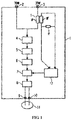
- Patent Literature 1 ( CN101982017A ) discloses a voltage conversion device, and Fig. 1 is a schematic diagram of the voltage conversion device of the Patent Literature 1. As shown in Fig. 1 , the voltage conversion device 1 has voltage connectors 2 and 3, and the alternating voltage fed from the voltage connector 2 or 3 sequentially goes through and is processed by an electromagnetic filter 4, a bridge rectifier 5, a direct voltage intermediate circuit 6, a half bridge inverter 7 and a resonant circuit 8 to become a direct voltage, and is output from output terminals 9 and 10 into an electrical equipment 11. Further relevant background art can be found in the patent literature documents: DE102008016752 A1 , US2013/164016 A1 , and EP1286455 A1 .
- the voltage conversion device 1 further has a transformer T, a resistor R and a control unit 12.
- a current flows through a primary winding W of the transformer T to generate an induced current in a secondary winding W' and generate a voltage difference across the resistor R.
- the control unit 12 detects a voltage difference across the resistor R, it can be determined that the alternating voltage is fed from the voltage connector 3, and a control signal corresponding to the voltage connector 3 is output to the half bridge inverter 7 to control the two switches in the half bridge inverter 7 to be alternately turned on, so that the voltage conversion device 1 outputs a corresponding direct voltage.
- control unit 12 detects that no voltage difference is generated across the resistor R, it can be determined that the alternating voltage is fed from the voltage connector 2, and a control signal corresponding to the voltage connector 2 is output to the half bridge inverter 7 to control the two switches in the half bridge inverter 7 to be alternately turned on, so that the voltage conversion device 1 outputs a corresponding direct voltage.
- Patent Literature 1 the circuit structure of Patent Literature 1 is complicated; when using the secondary side of the voltage conversion device to switch the control, the switching status needs to be fed back to the primary side, which increases the circuit complexity; when using the primary side of the voltage conversion device to switch the control, a two ways terminal and a jumper need to be set on the primary side, which also increases the circuit complexity.
- the determination unit further has a first diode D1 and a second diode D2, wherein the first diode D1 and the second diode D2 are connected in anti parallel between the first voltage connector and the second voltage connector, when the alternating voltage is fed to the voltage conversion device via the first voltage connector, both of the first diode D1 and the second diode D2 are turned off; and when the alternating voltage is fed to the voltage conversion device via the second voltage connector, the first diode D1 and the second diode D2 are alternately conducting forward in accordance with a flow of the alternating current.
- the first switch element Q1 is bipolar transistor, a base of the bipolar transistor is electrically connected to the second voltage connector via a first resistor R1 and an emitter of the bipolar transistor is electrically connected to the first voltage connector.
- a collector of the bipolar transistor is grounded via the second resistor R4.
- the determination unit further has a capacitor C1, and when the alternating voltage is fed to the voltage conversion device via the second voltage connector, the capacitor C1 maintains the voltage difference across the second resistor R4.
- the second switch element Q2 is a metal oxide semiconductor field effect (MOS-FET) transistor, and a gate of the metal oxide semiconductor field effect (MOS-FET) transistor and an ungrounded end of the second resistor R4 are electrically connected.
- MOS-FET metal oxide semiconductor field effect
- An advantageous effect of the embodiments of the present application is: a simple circuit can be used to determine the voltage connector for feeding and to perform a corresponding control to output a corresponding direct voltage or current.
- Embodiment 1 of this application provides a voltage conversion device configured to convert an input alternating voltage into a direct voltage or current and then output the same.
- the direct voltage or current output by the voltage conversion device may be provided to an electrical appliance, such as a light-emitting diode (LED).
- LED light-emitting diode
- Fig. 2 is a schematic diagram of the voltage conversion device of the embodiment.
- the voltage conversion device 200 may include: a first voltage connector n1, a second voltage connector n2, an electromagnetic filter unit 201, a conversion unit 202, a determination unit 203 and a control unit 204.
- the alternating voltage can be fed to the voltage conversion device 200 via the first voltage connector n1 or the second voltage connector n2;
- the electromagnetic filter unit 201 is configured to electromagnetically filter the input alternating voltage;
- the conversion unit 202 is configured to convert the voltage which has been electromagnetically filtered by the electromagnetic filter unit 201 into a direct voltage or current and output the same;
- the determination unit 203 is configured to determine which one of the first voltage connector n1 and the second voltage connector n2 is used to feed the alternating voltage into the voltage conversion device 200;
- the control unit 204 controls the conversion unit 202 based on a determination result of the determination unit 203 such that direct voltage or current output by the conversion unit 202 corresponds the determination result.
- the determination unit 203 is electrically connected to the first voltage connector n1 and is electrically connected to the second voltage connector n2 in this embodiment.
- the determination unit 203 is electrically connected to the first voltage connector n1 and is electrically connected to the second voltage connector n2 in this embodiment, it is possible to determine the voltage connector for feeding by using a simple circuit and to perform a corresponding control to output a corresponding direct voltage or current. Compared to the prior art, this embodiment can reduce the cost.
- the conversion unit 202 in this embodiment may have the same structure as the prior art.
- the conversion unit 202 can have a bridge rectifier, a direct voltage intermediate circuit, a half bridge inverter and a resonant circuit, etc.
- the half bridge inverter can have two alternating switches.
- the control unit 204 controls the duty ratio of the two alternating switches to make the conversion unit 202 output different direct voltages or currents.
- the conversion unit 202 can have other structures which will not be described again in this embodiment because reference can be made to the prior art.
- control unit 204 can control according to the determination result of the determination unit 203.
- the control unit 204 can be connected with the determination unit 203 to receive a signal output from the determination unit 203 and can also control correspondingly according to the signal output from the determination unit 203.
- the control unit 204 can be an integrated circuit (IC) in this embodiment, for example, an Application Specific Integrated Circuit (ASIC) or a microprocessor, etc.
- Fig. 3 is a schematic diagram of the determination unit 203 of this embodiment.
- the determination unit 203 may have a first switch element Q1 and a second switch element Q2.
- the first switch element Q1 and the second switch element Q2 are turned off.
- the first switch element Q1 is periodically turned on and the second switch element Q2 is kept turned on.
- the determination unit 203 may further have a first diode D1 and a second diode D2, where the first diode D1 and second diode D2 can be connected in anti parallel between the first voltage connector n1 and the second voltage connector n2.
- the first diode D1 and the second diode D2 can be connected in anti parallel between the first voltage connector n1 and the second voltage connector n2.
- the first switch element Q1 may be a bipolar transistor, for example, a PNP bipolar transistor.
- Abase B of the bipolar transistor can be electrically connected to the second voltage connector n2 via the first resistor R1, and an emitter E of the bipolar transistor can be electrically connected to the first voltage connector n1.
- a collector C of the bipolar transistor may be grounded via the second resistor R4.
- the voltage difference across the second resistor R4 can turn on the second switch element Q2.
- the second switch element Q2 can be a metal oxide semiconductor field effect (MOS-FET) transistor, and the gate of the second switch element Q2 and the ungrounded end of the second resistor R4 can be electrically connected.
- the drain of the second switch element Q2 can be connected with the control unit 204.
- the determination unit 203 may further have a capacitor C1, and when the alternating voltage is fed to the voltage conversion device via the second voltage connector, the capacitor C1 makes the voltage difference remain across the second resistor R4.
- this capacitor C1 can be connected with the second resistor R4 in parallel.
- the determination unit 203 may also have a third resistor R2, and this third resistor R2 can be connected between the collector of the first switch element Q1 and the second resistor R4.
- this embodiment can have more voltage connectors, and more determination units 203 can be set to determine whether an alternating voltage is fed from these voltage connectors.
- both the first diode D1 and the second diode D2 are cut off, that is, the base of the first switch element Q1 has no current flowing branch, which makes the first switch element Q1 cut off and therefore, the second switch element Q2 is turned off.
- the control unit 204 detects the cutoff of the second switch element Q2, and performs a control corresponding to the situation in which the alternating voltage is fed to the voltage conversion device 200 via the first voltage connector n1.
- the action of the determination unit 203 is as follows: In a certain half cycle of the alternating current, the first diode D1 is turned on, and the voltage difference between the emitter and the base of the first switch element Q1 is clamped by the first diode D1. Therefore, the first switch element Q1 is turned on during this half cycle in which D1 is turned on, and a current flows through the first switch element Q1. After the capacitor C1 is charged by the third resistor R2, the capacitor C1 stores a charge and a voltage difference is generated across the second resistor R4.
- This voltage difference is applied to the gate of the second switch element Q2, which causes the second switch element Q2 to stay turned on during this half cycle of the alternating current.
- the control unit 204 detects that the second switch element Q2 is turned on, and performs a control corresponding to the situation in which the alternating voltage is fed to the voltage conversion device 200 via the second voltage connector n2;
- the second diode D2 is turned on. This provides a path for the alternating voltage to enter the electromagnetic filter unit 201 via the second voltage connector n2.
- the first switch element Q1 is reverse-biased and is cut off, and does not charge the C1.
- the C1 stores a charge which maintains the voltage difference across the second resistor R4
- the second switch element Q2 is still turned on during this other half of the cycle. Therefore, the second switch element Q2 is kept turned on during the full cycle.
- the first switch element Q1 is turned on only during the half cycle in which the first diode D1 is conducting forward, and thus the first switch element Q1 is turned on periodically.
- N1 and N2 can be respectively a neutral line connected with an alternating current power supply
- L can be a live line connected with the alternating current power supply
- the determination unit 203 is electrically connected to the first voltage connector n1 and is electrically connected to the second voltage connector n2 in this embodiment, it is possible to determine the voltage connector for feeding by using a simple circuit and to perform a corresponding control to output a corresponding direct voltage or current. Compared to the prior art, this embodiment can reduce the cost.
Landscapes
- Engineering & Computer Science (AREA)
- Power Engineering (AREA)
- Physics & Mathematics (AREA)
- Electromagnetism (AREA)
- Dc-Dc Converters (AREA)
Claims (7)
- Spannungsumwandlungsvorrichtung (200), die zum Umwandeln einer Eingangswechselspannung in eine Gleichspannung oder einen Gleichstrom konfiguriert ist, wobei die Spannungsumwandlungsvorrichtung (200) mindestens einen ersten Spannungsanschluss (N1) und einen zweiten Spannungsanschluss (N2) umfasst, die beide konfiguriert sind, um an die Wechselspannung angeschlossen zu werden, wobei die Spannungsumwandlungsvorrichtung (200) ferner umfasst:eine elektromagnetische Filtereinheit (201), die zum elektromagnetischen Filtern der Wechselspannung konfiguriert ist, die entweder in den ersten Spannungsanschluss (N1) oder den zweiten Spannungsanschluss (N2) eingegeben wird;eine Umwandlungseinheit (202), die zum Umwandeln der Spannung, die durch die elektromagnetische Filtereinheit (201) gefiltert wurde, in eine Gleichspannung oder einen Gleichstrom und Ausgeben der- bzw. desselben konfiguriert ist;eine Bestimmungseinheit (203), die so konfiguriert ist, dass sie bestimmt, an welchen von dem ersten Spannungsanschluss (N1) und dem zweiten Spannungsanschluss (N2) die Wechselspannung angeschlossen ist;eine Steuereinheit (204), die so konfiguriert ist, dass sie die Umwandlungseinheit (202) basierend auf dem Bestimmungsergebnis der Bestimmungseinheit (203) derart steuert, dass die Gleichspannung oder der Gleichstrom, die/der von der Umwandlungseinheit (202) ausgeben wird, dem Bestimmungsergebnis entspricht,wobei die Bestimmungseinheit (203) mit dem ersten Spannungsanschluss (N1) und dem zweiten Spannungsanschluss (N2) elektrisch verbunden ist,dadurch gekennzeichnet, dass die Bestimmungseinheit (203) ein erstes Schaltelement (Q1) und ein zweites Schaltelement (Q2) umfasst, wobei die Bestimmungseinheit ferner eine erste Diode (D1) und eine Zweite Diode (D2) umfasst, wobei die erste Diode (D1) und die zweite Diode (D2) antiparallel zwischen den ersten Spannungsanschluss (N1) und den zweiten Spannungsanschluss (N2) geschaltet sind, wobei die erste Diode (D1) so ausgelegt ist, dass sie in einem bestimmten Halbzyklus der Wechselspannung einschaltet und das erste Schaltelement (Q1) nur im Halbzyklus der Wechselspannung einschaltet, und wobei die zweite Diode (D2) so ausgelegt ist, dass sie das erste Schaltelement in einem anderen Halbzyklus der Wechselspannung ein- und ausschaltet, unddadurch, dass die Bestimmungseinheit (203) ferner so konfiguriert ist, dass,- wenn die Wechselspannung über den ersten Spannungsanschluss (N1) in die Spannungsumwandlungsvorrichtung (202) eingespeist wird, sowohl das erste Schaltelement (Q1) als auch das zweite Schaltelement(Q2) ausgeschaltet werden; und- wenn die Wechselspannung über den zweiten Spannungsanschluss (N2) in die Spannungsumwandlungsvorrichtung (202) eingespeist wird, das erste Schaltelement (Q1) infolge von Leitung der ersten Diode (D1) nur im Halbzyklus der Wechselspannung periodisch eingeschaltet wird, was bewirkt, dass das zweite Schaltelement (Q2) während eines Vollzyklus, d. h. während des Halbzyklus und des anderen Halbzyklus, der Wechselspannung eingeschaltet wird, um dadurch der Steuereinheit (204) kontinuierlich die Verbindung der Wechselspannung mit dem zweiten Spannungsanschluss (N2) anzuzeigen.
- Spannungsumwandlungsvorrichtung nach Anspruch 1,
wobei die Bestimmungseinheit (203) ferner so konfiguriert ist, dass,- wenn die Wechselspannung über den ersten Spannungsanschluss (N1) in die Spannungsumwandlungsvorrichtung (200) eingespeist wird, sowohl die erste Diode (D1) als auch die zweite Diode (D2) ausgeschaltet werden; und- wenn die Wechselspannung über den zweien Spannungsanschluss (N2) in die Spannungsumwandlungsvorrichtung (200) eingespeist wird, die erste Diode (D1) und die zweite Diode (D2) gemäß einem Fluss eines Wechselstroms abwechselnd in Vorwärtsrichtung leitend sind. - Spannungsumwandlungsvorrichtung (200) nach Anspruch 2, wobei
das erste Schaltelement (Q1) ein Bipolartransistor ist, wobei eine Basis des Bipolartransistors mit dem zweiten Spannungsanschluss (N2) über einen ersten Widerstand (R1) elektrisch verbunden ist, und ein Emitter des Bipolartransistors mit dem ersten Spannungsanschluss (N1) elektrisch verbunden ist. - Spannungsumwandlungsvorrichtung (200) nach Anspruch 3, wobei
ein Kollektor des Bipolartransistors über einen zweiten Widerstand (R4) geerdet ist. - Spannungsumwandlungsvorrichtung (200) nach Anspruch 4, wobei
die Bestimmungseinheit (203) so konfiguriert ist, dass, wenn die Wechselspannung über den zweiten Spannungsanschluss (N2) in die Spannungsumwandlungsvorrichtung (200) eingespeist wird, eine Spannungsdifferenz über den zweiten Widerstand (R4) bewirkt, dass das zweite Schaltelement (Q2) einschaltet. - Spannungsumwandlungsvorrichtung (200) nach Anspruch 5, wobei
die Bestimmungseinheit (203) ferner einen Kondensator (C1) aufweist,
wobei die Bestimmungseinheit (203) so konfiguriert ist, dass, wenn die Wechselspannung über den zweiten Spannungsanschluss (N2) in die Spannungsumwandlungsvorrichtung (200) eingespeist wird, der Kondensator (C1) die Spannungsdifferenz über den zweiten Widerstands (R4) aufrechterhält. - Spannungsumwandlungsvorrichtung (200) nach Anspruch 5, wobei
das zweite Schaltelement (Q2) ein Metalloxid-Halbleiter-Feldeffekt-,MOS-FET-,Transistor ist, und ein Gate des Metalloxid-Halbleiter-Feldeffekt-,MOS-FET-,Transistors und ein nicht geerdetes Ende des zweiten Widerstands (R4) elektrisch verbunden sind.
Applications Claiming Priority (2)
| Application Number | Priority Date | Filing Date | Title |
|---|---|---|---|
| CN201611198701.6A CN108233738B (zh) | 2016-12-22 | 2016-12-22 | 电压转换装置 |
| PCT/CN2017/114578 WO2018113513A1 (zh) | 2016-12-22 | 2017-12-05 | 电压转换装置 |
Publications (3)
| Publication Number | Publication Date |
|---|---|
| EP3540931A1 EP3540931A1 (de) | 2019-09-18 |
| EP3540931A4 EP3540931A4 (de) | 2019-11-27 |
| EP3540931B1 true EP3540931B1 (de) | 2020-11-11 |
Family
ID=62624650
Family Applications (1)
| Application Number | Title | Priority Date | Filing Date |
|---|---|---|---|
| EP17884790.1A Active EP3540931B1 (de) | 2016-12-22 | 2017-12-05 | Spannungswandler |
Country Status (4)
| Country | Link |
|---|---|
| US (1) | US10630198B2 (de) |
| EP (1) | EP3540931B1 (de) |
| CN (1) | CN108233738B (de) |
| WO (1) | WO2018113513A1 (de) |
Families Citing this family (2)
| Publication number | Priority date | Publication date | Assignee | Title |
|---|---|---|---|---|
| US10990150B2 (en) * | 2018-07-24 | 2021-04-27 | Texas Instruments Incorporated | VCONN in power delivery chargers |
| CN116066613B (zh) * | 2022-10-11 | 2025-08-26 | 中国核动力研究设计院 | 供电电压可变的阀门控制系统、控制系统及可读存储介质 |
Family Cites Families (17)
| Publication number | Priority date | Publication date | Assignee | Title |
|---|---|---|---|---|
| WO2001067590A1 (fr) * | 2000-03-08 | 2001-09-13 | Kabushiki Kaisha Yaskawa Denki | Cycloconvertisseur mid et detecteur de pannes electriques |
| JP2009536014A (ja) * | 2006-05-01 | 2009-10-01 | ローズマウント・エアロスペース・インコーポレーテッド | 力率補正を有する汎用acまたはdc航空機装置電源 |
| CN101232170A (zh) * | 2007-01-26 | 2008-07-30 | 固纬电子实业股份有限公司 | 自动切换电路及具有自动切换功能的电源供应电路 |
| CN105553087A (zh) * | 2007-03-14 | 2016-05-04 | 佐尼特结构解决方案有限责任公司 | 用于将电力输送到具有电源线的设备的装置和方法 |
| DE102008016752A1 (de) | 2008-03-31 | 2009-10-01 | Tridonicatco Schweiz Ag | Erkennung der Belegung eines Anschlusses eines Betriebsgeräts für Leuchtmittel |
| CN201466987U (zh) * | 2009-06-09 | 2010-05-12 | 中国电力科学研究院 | 从输电线缆上获取电能的装置 |
| CN201536273U (zh) * | 2009-11-04 | 2010-07-28 | 佛山市柏克电力设备有限公司 | 一种双电源转换静态开关 |
| US8232680B2 (en) * | 2009-12-21 | 2012-07-31 | International Business Machines Corporation | Selecting a single AC source for a switching power supply |
| JP2013135588A (ja) * | 2011-12-27 | 2013-07-08 | Brother Ind Ltd | 電源システム及び画像形成装置 |
| KR101928856B1 (ko) * | 2012-08-09 | 2018-12-14 | 에이치피프린팅코리아 유한회사 | 전력 제어 장치 및 화상 형성 장치 |
| US8917042B2 (en) * | 2012-09-11 | 2014-12-23 | Regal Beloit America, Inc. | Methods and systems for reducing conducted electromagnetic interference |
| CN103683468B (zh) * | 2012-09-17 | 2016-08-24 | 台达电子工业股份有限公司 | 电源系统以及电源系统的控制方法 |
| US9112376B2 (en) * | 2012-12-28 | 2015-08-18 | Acbel Polytech Inc. | AC backup power system |
| CN203101494U (zh) * | 2013-03-15 | 2013-07-31 | 深圳市银河表计股份有限公司 | 交流市电掉电检测电路、设备及系统 |
| CN103257272B (zh) * | 2013-05-02 | 2016-03-02 | 江苏大学 | 一种交流供电电源掉电检测电路及检测方法 |
| CN104348370A (zh) * | 2013-08-01 | 2015-02-11 | 华为技术有限公司 | 电源变换模块、供电装置和供电方法 |
| CN204287446U (zh) * | 2014-12-09 | 2015-04-22 | 广东瑞德智能科技股份有限公司 | 一种掉电检测电路 |
-
2016
- 2016-12-22 CN CN201611198701.6A patent/CN108233738B/zh active Active
-
2017
- 2017-12-05 US US16/469,705 patent/US10630198B2/en active Active
- 2017-12-05 WO PCT/CN2017/114578 patent/WO2018113513A1/zh not_active Ceased
- 2017-12-05 EP EP17884790.1A patent/EP3540931B1/de active Active
Non-Patent Citations (1)
| Title |
|---|
| None * |
Also Published As
| Publication number | Publication date |
|---|---|
| US10630198B2 (en) | 2020-04-21 |
| CN108233738A (zh) | 2018-06-29 |
| US20190356237A1 (en) | 2019-11-21 |
| WO2018113513A1 (zh) | 2018-06-28 |
| EP3540931A1 (de) | 2019-09-18 |
| CN108233738B (zh) | 2020-11-17 |
| EP3540931A4 (de) | 2019-11-27 |
Similar Documents
| Publication | Publication Date | Title |
|---|---|---|
| JP6554325B2 (ja) | 絶縁同期整流型dc/dcコンバータおよびそのフィードバック回路、その同期整流コントローラ、それを用いた電源装置、電源アダプタおよび電子機器 | |
| JP6787989B2 (ja) | オープン出力保護を備えるドライバ | |
| JP6563729B2 (ja) | 絶縁同期整流型dc/dcコンバータ、それを用いた電源装置、電源アダプタおよび電子機器 | |
| JP6554321B2 (ja) | 絶縁同期整流型dc/dcコンバータおよびその同期整流コントローラ、それを用いた電源装置、電源アダプタおよび電子機器 | |
| US10615699B2 (en) | Voltage converter and voltage conversion method for reducing common mode noise | |
| JP6460479B2 (ja) | 制御電源装置および蓄電システム | |
| CN106910474B (zh) | 一种短路保护电路以及背光驱动电路 | |
| JP2015225825A (ja) | Ledランプ、led点灯装置、及びこれらを用いたled照明システム | |
| CN103780098B (zh) | 输出电压反馈电路、隔离式变换器和用于其的集成电路 | |
| US20190199126A1 (en) | Uninterruptible power supply apparatus | |
| CN100356676C (zh) | 用作应用电弧设备的电源装置 | |
| US10630198B2 (en) | Voltage converter | |
| RU2437204C1 (ru) | Устройство источника питания постоянного тока | |
| EP2690769B1 (de) | Stromversorgungsschaltung | |
| CN100530875C (zh) | 电气设备保护装置 | |
| US8237382B2 (en) | LED module and method for operating at least one LED | |
| US20200120768A1 (en) | Led driving circuit and led apparatus | |
| JP7011216B2 (ja) | 照明装置 | |
| KR100824451B1 (ko) | 전자 변압기 | |
| EP2849325A1 (de) | Wechselrichtereinheit für Photovoltaikmodule | |
| US11283366B2 (en) | Rectifier arrangement | |
| JP2009081901A (ja) | 過電圧保護装置 | |
| CN104125685A (zh) | 改型灯 | |
| CN211557589U (zh) | 控制电路和设备控制系统 | |
| US9024601B2 (en) | Voltage converting apparatus with low power consumption |
Legal Events
| Date | Code | Title | Description |
|---|---|---|---|
| STAA | Information on the status of an ep patent application or granted ep patent |
Free format text: STATUS: THE INTERNATIONAL PUBLICATION HAS BEEN MADE |
|
| PUAI | Public reference made under article 153(3) epc to a published international application that has entered the european phase |
Free format text: ORIGINAL CODE: 0009012 |
|
| STAA | Information on the status of an ep patent application or granted ep patent |
Free format text: STATUS: REQUEST FOR EXAMINATION WAS MADE |
|
| 17P | Request for examination filed |
Effective date: 20190612 |
|
| AK | Designated contracting states |
Kind code of ref document: A1 Designated state(s): AL AT BE BG CH CY CZ DE DK EE ES FI FR GB GR HR HU IE IS IT LI LT LU LV MC MK MT NL NO PL PT RO RS SE SI SK SM TR |
|
| AX | Request for extension of the european patent |
Extension state: BA ME |
|
| A4 | Supplementary search report drawn up and despatched |
Effective date: 20191024 |
|
| RIC1 | Information provided on ipc code assigned before grant |
Ipc: H02M 1/00 20060101AFI20191018BHEP Ipc: H05B 37/00 20060101ALI20191018BHEP Ipc: H02M 7/217 20060101ALI20191018BHEP Ipc: H05B 41/282 20060101ALI20191018BHEP |
|
| DAV | Request for validation of the european patent (deleted) | ||
| DAX | Request for extension of the european patent (deleted) | ||
| REG | Reference to a national code |
Ref country code: DE Ref legal event code: R079 Ref document number: 602017027571 Country of ref document: DE Free format text: PREVIOUS MAIN CLASS: H02M0007217000 Ipc: H02M0001000000 |
|
| GRAP | Despatch of communication of intention to grant a patent |
Free format text: ORIGINAL CODE: EPIDOSNIGR1 |
|
| STAA | Information on the status of an ep patent application or granted ep patent |
Free format text: STATUS: GRANT OF PATENT IS INTENDED |
|
| RIC1 | Information provided on ipc code assigned before grant |
Ipc: H05B 45/37 20200101ALI20200717BHEP Ipc: H02M 1/00 20060101AFI20200717BHEP Ipc: H05B 41/282 20060101ALI20200717BHEP Ipc: H02M 7/217 20060101ALI20200717BHEP |
|
| INTG | Intention to grant announced |
Effective date: 20200811 |
|
| GRAS | Grant fee paid |
Free format text: ORIGINAL CODE: EPIDOSNIGR3 |
|
| GRAA | (expected) grant |
Free format text: ORIGINAL CODE: 0009210 |
|
| STAA | Information on the status of an ep patent application or granted ep patent |
Free format text: STATUS: THE PATENT HAS BEEN GRANTED |
|
| AK | Designated contracting states |
Kind code of ref document: B1 Designated state(s): AL AT BE BG CH CY CZ DE DK EE ES FI FR GB GR HR HU IE IS IT LI LT LU LV MC MK MT NL NO PL PT RO RS SE SI SK SM TR |
|
| REG | Reference to a national code |
Ref country code: GB Ref legal event code: FG4D |
|
| REG | Reference to a national code |
Ref country code: CH Ref legal event code: EP |
|
| REG | Reference to a national code |
Ref country code: AT Ref legal event code: REF Ref document number: 1334391 Country of ref document: AT Kind code of ref document: T Effective date: 20201115 |
|
| REG | Reference to a national code |
Ref country code: DE Ref legal event code: R096 Ref document number: 602017027571 Country of ref document: DE |
|
| REG | Reference to a national code |
Ref country code: IE Ref legal event code: FG4D |
|
| REG | Reference to a national code |
Ref country code: NL Ref legal event code: MP Effective date: 20201111 |
|
| REG | Reference to a national code |
Ref country code: AT Ref legal event code: MK05 Ref document number: 1334391 Country of ref document: AT Kind code of ref document: T Effective date: 20201111 |
|
| PG25 | Lapsed in a contracting state [announced via postgrant information from national office to epo] |
Ref country code: NO Free format text: LAPSE BECAUSE OF FAILURE TO SUBMIT A TRANSLATION OF THE DESCRIPTION OR TO PAY THE FEE WITHIN THE PRESCRIBED TIME-LIMIT Effective date: 20210211 Ref country code: GR Free format text: LAPSE BECAUSE OF FAILURE TO SUBMIT A TRANSLATION OF THE DESCRIPTION OR TO PAY THE FEE WITHIN THE PRESCRIBED TIME-LIMIT Effective date: 20210212 Ref country code: FI Free format text: LAPSE BECAUSE OF FAILURE TO SUBMIT A TRANSLATION OF THE DESCRIPTION OR TO PAY THE FEE WITHIN THE PRESCRIBED TIME-LIMIT Effective date: 20201111 Ref country code: PT Free format text: LAPSE BECAUSE OF FAILURE TO SUBMIT A TRANSLATION OF THE DESCRIPTION OR TO PAY THE FEE WITHIN THE PRESCRIBED TIME-LIMIT Effective date: 20210311 Ref country code: RS Free format text: LAPSE BECAUSE OF FAILURE TO SUBMIT A TRANSLATION OF THE DESCRIPTION OR TO PAY THE FEE WITHIN THE PRESCRIBED TIME-LIMIT Effective date: 20201111 |
|
| PG25 | Lapsed in a contracting state [announced via postgrant information from national office to epo] |
Ref country code: AT Free format text: LAPSE BECAUSE OF FAILURE TO SUBMIT A TRANSLATION OF THE DESCRIPTION OR TO PAY THE FEE WITHIN THE PRESCRIBED TIME-LIMIT Effective date: 20201111 Ref country code: BG Free format text: LAPSE BECAUSE OF FAILURE TO SUBMIT A TRANSLATION OF THE DESCRIPTION OR TO PAY THE FEE WITHIN THE PRESCRIBED TIME-LIMIT Effective date: 20210211 Ref country code: IS Free format text: LAPSE BECAUSE OF FAILURE TO SUBMIT A TRANSLATION OF THE DESCRIPTION OR TO PAY THE FEE WITHIN THE PRESCRIBED TIME-LIMIT Effective date: 20210311 Ref country code: PL Free format text: LAPSE BECAUSE OF FAILURE TO SUBMIT A TRANSLATION OF THE DESCRIPTION OR TO PAY THE FEE WITHIN THE PRESCRIBED TIME-LIMIT Effective date: 20201111 Ref country code: LV Free format text: LAPSE BECAUSE OF FAILURE TO SUBMIT A TRANSLATION OF THE DESCRIPTION OR TO PAY THE FEE WITHIN THE PRESCRIBED TIME-LIMIT Effective date: 20201111 Ref country code: SE Free format text: LAPSE BECAUSE OF FAILURE TO SUBMIT A TRANSLATION OF THE DESCRIPTION OR TO PAY THE FEE WITHIN THE PRESCRIBED TIME-LIMIT Effective date: 20201111 |
|
| REG | Reference to a national code |
Ref country code: LT Ref legal event code: MG9D |
|
| PG25 | Lapsed in a contracting state [announced via postgrant information from national office to epo] |
Ref country code: HR Free format text: LAPSE BECAUSE OF FAILURE TO SUBMIT A TRANSLATION OF THE DESCRIPTION OR TO PAY THE FEE WITHIN THE PRESCRIBED TIME-LIMIT Effective date: 20201111 |
|
| PG25 | Lapsed in a contracting state [announced via postgrant information from national office to epo] |
Ref country code: SK Free format text: LAPSE BECAUSE OF FAILURE TO SUBMIT A TRANSLATION OF THE DESCRIPTION OR TO PAY THE FEE WITHIN THE PRESCRIBED TIME-LIMIT Effective date: 20201111 Ref country code: RO Free format text: LAPSE BECAUSE OF FAILURE TO SUBMIT A TRANSLATION OF THE DESCRIPTION OR TO PAY THE FEE WITHIN THE PRESCRIBED TIME-LIMIT Effective date: 20201111 Ref country code: SM Free format text: LAPSE BECAUSE OF FAILURE TO SUBMIT A TRANSLATION OF THE DESCRIPTION OR TO PAY THE FEE WITHIN THE PRESCRIBED TIME-LIMIT Effective date: 20201111 Ref country code: EE Free format text: LAPSE BECAUSE OF FAILURE TO SUBMIT A TRANSLATION OF THE DESCRIPTION OR TO PAY THE FEE WITHIN THE PRESCRIBED TIME-LIMIT Effective date: 20201111 Ref country code: CZ Free format text: LAPSE BECAUSE OF FAILURE TO SUBMIT A TRANSLATION OF THE DESCRIPTION OR TO PAY THE FEE WITHIN THE PRESCRIBED TIME-LIMIT Effective date: 20201111 Ref country code: LT Free format text: LAPSE BECAUSE OF FAILURE TO SUBMIT A TRANSLATION OF THE DESCRIPTION OR TO PAY THE FEE WITHIN THE PRESCRIBED TIME-LIMIT Effective date: 20201111 |
|
| REG | Reference to a national code |
Ref country code: CH Ref legal event code: PL |
|
| REG | Reference to a national code |
Ref country code: DE Ref legal event code: R097 Ref document number: 602017027571 Country of ref document: DE |
|
| PG25 | Lapsed in a contracting state [announced via postgrant information from national office to epo] |
Ref country code: MC Free format text: LAPSE BECAUSE OF FAILURE TO SUBMIT A TRANSLATION OF THE DESCRIPTION OR TO PAY THE FEE WITHIN THE PRESCRIBED TIME-LIMIT Effective date: 20201111 Ref country code: DK Free format text: LAPSE BECAUSE OF FAILURE TO SUBMIT A TRANSLATION OF THE DESCRIPTION OR TO PAY THE FEE WITHIN THE PRESCRIBED TIME-LIMIT Effective date: 20201111 |
|
| REG | Reference to a national code |
Ref country code: BE Ref legal event code: MM Effective date: 20201231 |
|
| PLBE | No opposition filed within time limit |
Free format text: ORIGINAL CODE: 0009261 |
|
| STAA | Information on the status of an ep patent application or granted ep patent |
Free format text: STATUS: NO OPPOSITION FILED WITHIN TIME LIMIT |
|
| 26N | No opposition filed |
Effective date: 20210812 |
|
| PG25 | Lapsed in a contracting state [announced via postgrant information from national office to epo] |
Ref country code: NL Free format text: LAPSE BECAUSE OF FAILURE TO SUBMIT A TRANSLATION OF THE DESCRIPTION OR TO PAY THE FEE WITHIN THE PRESCRIBED TIME-LIMIT Effective date: 20201111 Ref country code: AL Free format text: LAPSE BECAUSE OF FAILURE TO SUBMIT A TRANSLATION OF THE DESCRIPTION OR TO PAY THE FEE WITHIN THE PRESCRIBED TIME-LIMIT Effective date: 20201111 Ref country code: IE Free format text: LAPSE BECAUSE OF NON-PAYMENT OF DUE FEES Effective date: 20201205 Ref country code: IT Free format text: LAPSE BECAUSE OF FAILURE TO SUBMIT A TRANSLATION OF THE DESCRIPTION OR TO PAY THE FEE WITHIN THE PRESCRIBED TIME-LIMIT Effective date: 20201111 Ref country code: LU Free format text: LAPSE BECAUSE OF NON-PAYMENT OF DUE FEES Effective date: 20201205 |
|
| PG25 | Lapsed in a contracting state [announced via postgrant information from national office to epo] |
Ref country code: CH Free format text: LAPSE BECAUSE OF NON-PAYMENT OF DUE FEES Effective date: 20201231 Ref country code: SI Free format text: LAPSE BECAUSE OF FAILURE TO SUBMIT A TRANSLATION OF THE DESCRIPTION OR TO PAY THE FEE WITHIN THE PRESCRIBED TIME-LIMIT Effective date: 20201111 Ref country code: LI Free format text: LAPSE BECAUSE OF NON-PAYMENT OF DUE FEES Effective date: 20201231 |
|
| PG25 | Lapsed in a contracting state [announced via postgrant information from national office to epo] |
Ref country code: ES Free format text: LAPSE BECAUSE OF FAILURE TO SUBMIT A TRANSLATION OF THE DESCRIPTION OR TO PAY THE FEE WITHIN THE PRESCRIBED TIME-LIMIT Effective date: 20201111 |
|
| PG25 | Lapsed in a contracting state [announced via postgrant information from national office to epo] |
Ref country code: IS Free format text: LAPSE BECAUSE OF FAILURE TO SUBMIT A TRANSLATION OF THE DESCRIPTION OR TO PAY THE FEE WITHIN THE PRESCRIBED TIME-LIMIT Effective date: 20210311 Ref country code: TR Free format text: LAPSE BECAUSE OF FAILURE TO SUBMIT A TRANSLATION OF THE DESCRIPTION OR TO PAY THE FEE WITHIN THE PRESCRIBED TIME-LIMIT Effective date: 20201111 Ref country code: MT Free format text: LAPSE BECAUSE OF FAILURE TO SUBMIT A TRANSLATION OF THE DESCRIPTION OR TO PAY THE FEE WITHIN THE PRESCRIBED TIME-LIMIT Effective date: 20201111 Ref country code: CY Free format text: LAPSE BECAUSE OF FAILURE TO SUBMIT A TRANSLATION OF THE DESCRIPTION OR TO PAY THE FEE WITHIN THE PRESCRIBED TIME-LIMIT Effective date: 20201111 |
|
| PG25 | Lapsed in a contracting state [announced via postgrant information from national office to epo] |
Ref country code: MK Free format text: LAPSE BECAUSE OF FAILURE TO SUBMIT A TRANSLATION OF THE DESCRIPTION OR TO PAY THE FEE WITHIN THE PRESCRIBED TIME-LIMIT Effective date: 20201111 |
|
| PG25 | Lapsed in a contracting state [announced via postgrant information from national office to epo] |
Ref country code: BE Free format text: LAPSE BECAUSE OF NON-PAYMENT OF DUE FEES Effective date: 20201231 |
|
| P01 | Opt-out of the competence of the unified patent court (upc) registered |
Effective date: 20230530 |
|
| PGFP | Annual fee paid to national office [announced via postgrant information from national office to epo] |
Ref country code: GB Payment date: 20241217 Year of fee payment: 8 |
|
| PGFP | Annual fee paid to national office [announced via postgrant information from national office to epo] |
Ref country code: FR Payment date: 20241227 Year of fee payment: 8 |
|
| REG | Reference to a national code |
Ref country code: DE Ref legal event code: R084 Ref document number: 602017027571 Country of ref document: DE |
|
| PGFP | Annual fee paid to national office [announced via postgrant information from national office to epo] |
Ref country code: DE Payment date: 20251229 Year of fee payment: 9 |