EP3540941A1 - Verbundsubstrat, oberflächenschallwellenvorrichtung und verfahren zur herstellung des verbundsubstrats - Google Patents
Verbundsubstrat, oberflächenschallwellenvorrichtung und verfahren zur herstellung des verbundsubstrats Download PDFInfo
- Publication number
- EP3540941A1 EP3540941A1 EP17870478.9A EP17870478A EP3540941A1 EP 3540941 A1 EP3540941 A1 EP 3540941A1 EP 17870478 A EP17870478 A EP 17870478A EP 3540941 A1 EP3540941 A1 EP 3540941A1
- Authority
- EP
- European Patent Office
- Prior art keywords
- intermediate layer
- composite substrate
- substrate according
- substrate
- manufacturing
- Prior art date
- Legal status (The legal status is an assumption and is not a legal conclusion. Google has not performed a legal analysis and makes no representation as to the accuracy of the status listed.)
- Granted
Links
Images


Classifications
-
- H—ELECTRICITY
- H03—ELECTRONIC CIRCUITRY
- H03H—IMPEDANCE NETWORKS, e.g. RESONANT CIRCUITS; RESONATORS
- H03H3/00—Apparatus or processes specially adapted for the manufacture of impedance networks, resonating circuits, resonators
- H03H3/007—Apparatus or processes specially adapted for the manufacture of impedance networks, resonating circuits, resonators for the manufacture of electromechanical resonators or networks
- H03H3/08—Apparatus or processes specially adapted for the manufacture of impedance networks, resonating circuits, resonators for the manufacture of electromechanical resonators or networks for the manufacture of resonators or networks using surface acoustic waves
- H03H3/10—Apparatus or processes specially adapted for the manufacture of impedance networks, resonating circuits, resonators for the manufacture of electromechanical resonators or networks for the manufacture of resonators or networks using surface acoustic waves for obtaining desired frequency or temperature coefficient
-
- H—ELECTRICITY
- H10—SEMICONDUCTOR DEVICES; ELECTRIC SOLID-STATE DEVICES NOT OTHERWISE PROVIDED FOR
- H10N—ELECTRIC SOLID-STATE DEVICES NOT OTHERWISE PROVIDED FOR
- H10N30/00—Piezoelectric or electrostrictive devices
- H10N30/01—Manufacture or treatment
- H10N30/07—Forming of piezoelectric or electrostrictive parts or bodies on an electrical element or another base
- H10N30/072—Forming of piezoelectric or electrostrictive parts or bodies on an electrical element or another base by laminating or bonding of piezoelectric or electrostrictive bodies
- H10N30/073—Forming of piezoelectric or electrostrictive parts or bodies on an electrical element or another base by laminating or bonding of piezoelectric or electrostrictive bodies by fusion of metals or by adhesives
-
- H—ELECTRICITY
- H10—SEMICONDUCTOR DEVICES; ELECTRIC SOLID-STATE DEVICES NOT OTHERWISE PROVIDED FOR
- H10N—ELECTRIC SOLID-STATE DEVICES NOT OTHERWISE PROVIDED FOR
- H10N30/00—Piezoelectric or electrostrictive devices
- H10N30/704—Piezoelectric or electrostrictive devices based on piezoelectric or electrostrictive films or coatings
- H10N30/706—Piezoelectric or electrostrictive devices based on piezoelectric or electrostrictive films or coatings characterised by the underlying bases, e.g. substrates
- H10N30/708—Intermediate layers, e.g. barrier, adhesion or growth control buffer layers
-
- C—CHEMISTRY; METALLURGY
- C01—INORGANIC CHEMISTRY
- C01B—NON-METALLIC ELEMENTS; COMPOUNDS THEREOF; METALLOIDS OR COMPOUNDS THEREOF NOT COVERED BY SUBCLASS C01C
- C01B33/00—Silicon; Compounds thereof
- C01B33/113—Silicon oxides; Hydrates thereof
- C01B33/12—Silica; Hydrates thereof, e.g. lepidoic silicic acid
-
- H—ELECTRICITY
- H03—ELECTRONIC CIRCUITRY
- H03H—IMPEDANCE NETWORKS, e.g. RESONANT CIRCUITS; RESONATORS
- H03H9/00—Networks comprising electromechanical or electro-acoustic elements; Electromechanical resonators
- H03H9/02—Details
- H03H9/02535—Details of surface acoustic wave devices
- H03H9/02543—Characteristics of substrate, e.g. cutting angles
- H03H9/02559—Characteristics of substrate, e.g. cutting angles of lithium niobate or lithium-tantalate substrates
-
- H—ELECTRICITY
- H03—ELECTRONIC CIRCUITRY
- H03H—IMPEDANCE NETWORKS, e.g. RESONANT CIRCUITS; RESONATORS
- H03H9/00—Networks comprising electromechanical or electro-acoustic elements; Electromechanical resonators
- H03H9/02—Details
- H03H9/02535—Details of surface acoustic wave devices
- H03H9/02818—Means for compensation or elimination of undesirable effects
- H03H9/02826—Means for compensation or elimination of undesirable effects of adherence
-
- H—ELECTRICITY
- H03—ELECTRONIC CIRCUITRY
- H03H—IMPEDANCE NETWORKS, e.g. RESONANT CIRCUITS; RESONATORS
- H03H9/00—Networks comprising electromechanical or electro-acoustic elements; Electromechanical resonators
- H03H9/02—Details
- H03H9/02535—Details of surface acoustic wave devices
- H03H9/02818—Means for compensation or elimination of undesirable effects
- H03H9/02897—Means for compensation or elimination of undesirable effects of strain or mechanical damage, e.g. strain due to bending influence
-
- H—ELECTRICITY
- H03—ELECTRONIC CIRCUITRY
- H03H—IMPEDANCE NETWORKS, e.g. RESONANT CIRCUITS; RESONATORS
- H03H9/00—Networks comprising electromechanical or electro-acoustic elements; Electromechanical resonators
- H03H9/02—Details
- H03H9/02535—Details of surface acoustic wave devices
- H03H9/02984—Protection measures against damaging
-
- H—ELECTRICITY
- H03—ELECTRONIC CIRCUITRY
- H03H—IMPEDANCE NETWORKS, e.g. RESONANT CIRCUITS; RESONATORS
- H03H9/00—Networks comprising electromechanical or electro-acoustic elements; Electromechanical resonators
- H03H9/25—Constructional features of resonators using surface acoustic waves
-
- H—ELECTRICITY
- H10—SEMICONDUCTOR DEVICES; ELECTRIC SOLID-STATE DEVICES NOT OTHERWISE PROVIDED FOR
- H10D—INORGANIC ELECTRIC SEMICONDUCTOR DEVICES
- H10D86/00—Integrated devices formed in or on insulating or conducting substrates, e.g. formed in silicon-on-insulator [SOI] substrates or on stainless steel or glass substrates
-
- H—ELECTRICITY
- H10—SEMICONDUCTOR DEVICES; ELECTRIC SOLID-STATE DEVICES NOT OTHERWISE PROVIDED FOR
- H10N—ELECTRIC SOLID-STATE DEVICES NOT OTHERWISE PROVIDED FOR
- H10N30/00—Piezoelectric or electrostrictive devices
- H10N30/01—Manufacture or treatment
- H10N30/07—Forming of piezoelectric or electrostrictive parts or bodies on an electrical element or another base
- H10N30/072—Forming of piezoelectric or electrostrictive parts or bodies on an electrical element or another base by laminating or bonding of piezoelectric or electrostrictive bodies
-
- H—ELECTRICITY
- H10—SEMICONDUCTOR DEVICES; ELECTRIC SOLID-STATE DEVICES NOT OTHERWISE PROVIDED FOR
- H10N—ELECTRIC SOLID-STATE DEVICES NOT OTHERWISE PROVIDED FOR
- H10N30/00—Piezoelectric or electrostrictive devices
- H10N30/01—Manufacture or treatment
- H10N30/07—Forming of piezoelectric or electrostrictive parts or bodies on an electrical element or another base
- H10N30/074—Forming of piezoelectric or electrostrictive parts or bodies on an electrical element or another base by depositing piezoelectric or electrostrictive layers, e.g. aerosol or screen printing
- H10N30/079—Forming of piezoelectric or electrostrictive parts or bodies on an electrical element or another base by depositing piezoelectric or electrostrictive layers, e.g. aerosol or screen printing using intermediate layers, e.g. for growth control
-
- H—ELECTRICITY
- H10—SEMICONDUCTOR DEVICES; ELECTRIC SOLID-STATE DEVICES NOT OTHERWISE PROVIDED FOR
- H10N—ELECTRIC SOLID-STATE DEVICES NOT OTHERWISE PROVIDED FOR
- H10N30/00—Piezoelectric or electrostrictive devices
- H10N30/01—Manufacture or treatment
- H10N30/08—Shaping or machining of piezoelectric or electrostrictive bodies
- H10N30/085—Shaping or machining of piezoelectric or electrostrictive bodies by machining
- H10N30/086—Shaping or machining of piezoelectric or electrostrictive bodies by machining by polishing or grinding
-
- H—ELECTRICITY
- H10—SEMICONDUCTOR DEVICES; ELECTRIC SOLID-STATE DEVICES NOT OTHERWISE PROVIDED FOR
- H10P—GENERIC PROCESSES OR APPARATUS FOR THE MANUFACTURE OR TREATMENT OF DEVICES COVERED BY CLASS H10
- H10P10/00—Bonding of wafers, substrates or parts of devices
- H10P10/12—Bonding of semiconductor wafers or semiconductor substrates to semiconductor wafers or semiconductor substrates
-
- H—ELECTRICITY
- H10—SEMICONDUCTOR DEVICES; ELECTRIC SOLID-STATE DEVICES NOT OTHERWISE PROVIDED FOR
- H10P—GENERIC PROCESSES OR APPARATUS FOR THE MANUFACTURE OR TREATMENT OF DEVICES COVERED BY CLASS H10
- H10P14/00—Formation of materials, e.g. in the shape of layers or pillars
- H10P14/20—Formation of materials, e.g. in the shape of layers or pillars of semiconductor materials
- H10P14/29—Formation of materials, e.g. in the shape of layers or pillars of semiconductor materials characterised by the substrates
- H10P14/2901—Materials
- H10P14/2902—Materials being Group IVA materials
- H10P14/2905—Silicon, silicon germanium or germanium
-
- H—ELECTRICITY
- H10—SEMICONDUCTOR DEVICES; ELECTRIC SOLID-STATE DEVICES NOT OTHERWISE PROVIDED FOR
- H10P—GENERIC PROCESSES OR APPARATUS FOR THE MANUFACTURE OR TREATMENT OF DEVICES COVERED BY CLASS H10
- H10P14/00—Formation of materials, e.g. in the shape of layers or pillars
- H10P14/20—Formation of materials, e.g. in the shape of layers or pillars of semiconductor materials
- H10P14/34—Deposited materials, e.g. layers
- H10P14/3451—Structure
- H10P14/3452—Microstructure
- H10P14/3458—Monocrystalline
-
- H—ELECTRICITY
- H10—SEMICONDUCTOR DEVICES; ELECTRIC SOLID-STATE DEVICES NOT OTHERWISE PROVIDED FOR
- H10P—GENERIC PROCESSES OR APPARATUS FOR THE MANUFACTURE OR TREATMENT OF DEVICES COVERED BY CLASS H10
- H10P90/00—Preparation of wafers not covered by a single main group of this subclass, e.g. wafer reinforcement
- H10P90/19—Preparing inhomogeneous wafers
- H10P90/1904—Preparing vertically inhomogeneous wafers
- H10P90/1906—Preparing SOI wafers
- H10P90/1914—Preparing SOI wafers using bonding
- H10P90/1916—Preparing SOI wafers using bonding with separation or delamination along an ion implanted layer, e.g. Smart-cut
-
- H—ELECTRICITY
- H10—SEMICONDUCTOR DEVICES; ELECTRIC SOLID-STATE DEVICES NOT OTHERWISE PROVIDED FOR
- H10P—GENERIC PROCESSES OR APPARATUS FOR THE MANUFACTURE OR TREATMENT OF DEVICES COVERED BY CLASS H10
- H10P95/00—Generic processes or apparatus for manufacture or treatments not covered by the other groups of this subclass
-
- H—ELECTRICITY
- H10—SEMICONDUCTOR DEVICES; ELECTRIC SOLID-STATE DEVICES NOT OTHERWISE PROVIDED FOR
- H10W—GENERIC PACKAGES, INTERCONNECTIONS, CONNECTORS OR OTHER CONSTRUCTIONAL DETAILS OF DEVICES COVERED BY CLASS H10
- H10W10/00—Isolation regions in semiconductor bodies between components of integrated devices
- H10W10/10—Isolation regions comprising dielectric materials
- H10W10/181—Semiconductor-on-insulator [SOI] isolation regions, e.g. buried oxide regions of SOI wafers
-
- H—ELECTRICITY
- H03—ELECTRONIC CIRCUITRY
- H03H—IMPEDANCE NETWORKS, e.g. RESONANT CIRCUITS; RESONATORS
- H03H3/00—Apparatus or processes specially adapted for the manufacture of impedance networks, resonating circuits, resonators
- H03H3/007—Apparatus or processes specially adapted for the manufacture of impedance networks, resonating circuits, resonators for the manufacture of electromechanical resonators or networks
- H03H3/08—Apparatus or processes specially adapted for the manufacture of impedance networks, resonating circuits, resonators for the manufacture of electromechanical resonators or networks for the manufacture of resonators or networks using surface acoustic waves
-
- H—ELECTRICITY
- H03—ELECTRONIC CIRCUITRY
- H03H—IMPEDANCE NETWORKS, e.g. RESONANT CIRCUITS; RESONATORS
- H03H9/00—Networks comprising electromechanical or electro-acoustic elements; Electromechanical resonators
- H03H9/02—Details
- H03H9/02535—Details of surface acoustic wave devices
- H03H9/02543—Characteristics of substrate, e.g. cutting angles
- H03H9/02574—Characteristics of substrate, e.g. cutting angles of combined substrates, multilayered substrates, piezoelectrical layers on not-piezoelectrical substrate
-
- H—ELECTRICITY
- H03—ELECTRONIC CIRCUITRY
- H03H—IMPEDANCE NETWORKS, e.g. RESONANT CIRCUITS; RESONATORS
- H03H9/00—Networks comprising electromechanical or electro-acoustic elements; Electromechanical resonators
- H03H9/02—Details
- H03H9/02535—Details of surface acoustic wave devices
- H03H9/02818—Means for compensation or elimination of undesirable effects
- H03H9/02834—Means for compensation or elimination of undesirable effects of temperature influence
-
- H—ELECTRICITY
- H03—ELECTRONIC CIRCUITRY
- H03H—IMPEDANCE NETWORKS, e.g. RESONANT CIRCUITS; RESONATORS
- H03H9/00—Networks comprising electromechanical or electro-acoustic elements; Electromechanical resonators
- H03H9/02—Details
- H03H9/02535—Details of surface acoustic wave devices
- H03H9/02818—Means for compensation or elimination of undesirable effects
- H03H9/02866—Means for compensation or elimination of undesirable effects of bulk wave excitation and reflections
Definitions
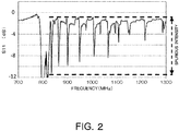
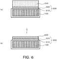
- a first intermediate layer 310 including thermally synthesized silica is formed on the surface of the support substrate 100 ( Fig. 4(b) ).
- a thermally synthesized silica layer having the same material as the first intermediate layer 310 may be formed on the back surface of the support substrate 100.
- the silica layer on the back surface may be appropriately removed using hydrofluoric acid, for example.
- a thermally oxidized silica film to be the first intermediate layer 310 can be formed by thermal oxidation of a silicon substrate. Since thermally oxidized silica is grown at high temperature, the thermally oxidized silica has the properties of being fine with few impurities and can absorb gases to some extent.
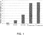
- An LT substrate in a diameter of six inches having a roughness of about 230 nm (in P-V, about 1.7 ⁇ m) in Ra was prepared.
- a process was repeated for a plurality of times in which a solution of an organic silicon compound was spin-coated and heated at a temperature of 350°C, and hence an SiO 2 layer in a thickness of about 5 ⁇ m was obtained.
- the solution of the organic silicon compound used here is two types of perhydropolysilazane (a solvent was dibutylether) and methyltrimethoxysilane (a solvent was propylene glycol monoethyl ether).
- a plasma activation process was applied to both of the SiO 2 film deposited on the LT substrate and the sintered SiO 2 film deposited on the sapphire substrate, the two substrates were bonded to each other and subjected to heat treatment at a temperature of 120°C, the LT was ground and polished to reduce the thickness to 20 ⁇ m, and then a composite substrate was obtained.
Landscapes
- Physics & Mathematics (AREA)
- Acoustics & Sound (AREA)
- Engineering & Computer Science (AREA)
- Manufacturing & Machinery (AREA)
- Chemical & Material Sciences (AREA)
- Organic Chemistry (AREA)
- Inorganic Chemistry (AREA)
- Materials Engineering (AREA)
- Surface Acoustic Wave Elements And Circuit Networks Thereof (AREA)
- Silicon Compounds (AREA)
- Physical Vapour Deposition (AREA)
- Chemical Vapour Deposition (AREA)
Applications Claiming Priority (3)
| Application Number | Priority Date | Filing Date | Title |
|---|---|---|---|
| JP2016220238 | 2016-11-11 | ||
| JP2017089666 | 2017-04-28 | ||
| PCT/JP2017/036707 WO2018088093A1 (ja) | 2016-11-11 | 2017-10-10 | 複合基板、表面弾性波デバイスおよび複合基板の製造方法 |
Publications (3)
| Publication Number | Publication Date |
|---|---|
| EP3540941A1 true EP3540941A1 (de) | 2019-09-18 |
| EP3540941A4 EP3540941A4 (de) | 2020-06-17 |
| EP3540941B1 EP3540941B1 (de) | 2022-09-07 |
Family
ID=62109526
Family Applications (1)
| Application Number | Title | Priority Date | Filing Date |
|---|---|---|---|
| EP17870478.9A Active EP3540941B1 (de) | 2016-11-11 | 2017-10-10 | Verbundsubstrat für oberflächenschallwellenbauelemente und verfahren zur herstellung des verbundsubstrats |
Country Status (7)
| Country | Link |
|---|---|
| US (2) | US11800805B2 (de) |
| EP (1) | EP3540941B1 (de) |
| JP (1) | JP6770089B2 (de) |
| KR (1) | KR102433349B1 (de) |
| CN (1) | CN109891747B (de) |
| TW (1) | TWI776822B (de) |
| WO (1) | WO2018088093A1 (de) |
Cited By (1)
| Publication number | Priority date | Publication date | Assignee | Title |
|---|---|---|---|---|
| EP3846343A4 (de) * | 2018-08-30 | 2022-05-25 | Shin-Etsu Chemical Co., Ltd. | Verbundsubstrat und verfahren zur herstellung des verbundsubstrats |
Families Citing this family (24)
| Publication number | Priority date | Publication date | Assignee | Title |
|---|---|---|---|---|
| US11095266B2 (en) * | 2016-10-07 | 2021-08-17 | Qorvo Us, Inc. | Slanted apodization for acoustic wave devices |
| JP7152711B2 (ja) * | 2018-06-20 | 2022-10-13 | 日本電産マシンツール株式会社 | 接合基板の製造方法及び接合基板 |
| DE112019002418B4 (de) | 2018-06-22 | 2022-06-15 | Ngk Insulators, Ltd. | Verbundener Körper und Elastikwellenelement |
| TWI815970B (zh) * | 2018-11-09 | 2023-09-21 | 日商日本碍子股份有限公司 | 壓電性材料基板與支持基板的接合體、及其製造方法 |
| JP2020090420A (ja) * | 2018-12-07 | 2020-06-11 | 住友金属鉱山株式会社 | 黒鉛製またはセラミックス製の基板、基板の製造方法、炭化珪素の成膜方法および炭化珪素基板の製造方法 |
| WO2021002046A1 (ja) * | 2019-07-03 | 2021-01-07 | 日本碍子株式会社 | 接合体および弾性波素子 |
| US11183987B2 (en) * | 2019-09-26 | 2021-11-23 | Avago Technologies International Sales Pte. Limited | Acoustic resonator device |
| CN114641933A (zh) * | 2019-11-06 | 2022-06-17 | 株式会社村田制作所 | 弹性波装置 |
| JP7271458B2 (ja) * | 2020-02-03 | 2023-05-11 | 信越化学工業株式会社 | 複合基板の製造方法 |
| JP7274442B2 (ja) * | 2020-04-02 | 2023-05-16 | 信越化学工業株式会社 | 複合基板およびその製造方法 |
| JP7262415B2 (ja) * | 2020-04-03 | 2023-04-21 | 信越化学工業株式会社 | 複合基板およびその製造方法 |
| CN113540339B (zh) * | 2020-04-21 | 2024-07-12 | 济南晶正电子科技有限公司 | 一种制备压电复合薄膜的方法及压电复合薄膜 |
| JP7336413B2 (ja) * | 2020-04-30 | 2023-08-31 | 信越化学工業株式会社 | 複合基板の製造方法および複合基板 |
| JP7402112B2 (ja) | 2020-05-08 | 2023-12-20 | 信越化学工業株式会社 | 圧電性単結晶膜を備えた複合基板の製造方法 |
| JP7262421B2 (ja) * | 2020-05-08 | 2023-04-21 | 信越化学工業株式会社 | 圧電体複合基板およびその製造方法 |
| CN111880124B (zh) * | 2020-07-10 | 2021-11-19 | 中国科学院上海微系统与信息技术研究所 | 一种高频可调节磁场探测器的制备方法 |
| KR102430218B1 (ko) * | 2020-10-20 | 2022-08-11 | 한국전자기술연구원 | AlN(질화알루미늄) 박막 증착 방법 |
| CN112382563A (zh) * | 2020-11-13 | 2021-02-19 | 济南晶正电子科技有限公司 | 离子注入薄膜晶圆剥离方法、单晶薄膜及电子元器件 |
| JP7290156B2 (ja) * | 2021-02-05 | 2023-06-13 | 信越半導体株式会社 | 窒化物半導体基板及びその製造方法 |
| JP7695335B2 (ja) * | 2021-02-19 | 2025-06-18 | 信越化学工業株式会社 | 複合ウェーハおよびその製造方法 |
| KR20230128099A (ko) * | 2021-02-19 | 2023-09-01 | 신에쓰 가가꾸 고교 가부시끼가이샤 | 복합 웨이퍼 및 그 제조 방법 |
| FR3130073B1 (fr) * | 2021-12-06 | 2024-09-06 | Commissariat Energie Atomique | Procédé de transfert d’une couche |
| CN117460388B (zh) * | 2023-12-25 | 2024-07-23 | 天通瑞宏科技有限公司 | 一种复合衬底及其制备方法 |
| JP2026045923A (ja) * | 2024-08-30 | 2026-03-13 | グローバルウェーハズ・ジャパン株式会社 | 複合基板の製造方法、複合基板、および弾性波デバイス |
Family Cites Families (20)
| Publication number | Priority date | Publication date | Assignee | Title |
|---|---|---|---|---|
| JP2001053579A (ja) * | 1999-06-02 | 2001-02-23 | Matsushita Electric Ind Co Ltd | 弾性表面波素子と移動体通信機器 |
| WO2003052840A1 (en) | 2001-12-18 | 2003-06-26 | Matsushita Electric Industrial Co., Ltd. | Piezoelectric element, ink jet head, angular velocity sensor, manufacturing method thereof, and ink jet type recording apparatus |
| US7105980B2 (en) * | 2002-07-03 | 2006-09-12 | Sawtek, Inc. | Saw filter device and method employing normal temperature bonding for producing desirable filter production and performance characteristics |
| JP4590854B2 (ja) * | 2003-10-28 | 2010-12-01 | セイコーエプソン株式会社 | 圧電体デバイスの製造方法 |
| JP2005229455A (ja) * | 2004-02-16 | 2005-08-25 | Shin Etsu Chem Co Ltd | 複合圧電基板 |
| JP2006303940A (ja) * | 2005-04-21 | 2006-11-02 | Nec Tokin Corp | 複合圧電基板及びその製造方法 |
| JP3863551B1 (ja) * | 2005-12-24 | 2006-12-27 | 渡邊 隆彌 | 水晶エピタキシャル薄膜 |
| JP5455595B2 (ja) * | 2008-12-11 | 2014-03-26 | 信越化学工業株式会社 | 貼り合わせウェーハの製造方法 |
| JP6074130B2 (ja) * | 2011-03-24 | 2017-02-01 | セイコーエプソン株式会社 | 圧電素子の製造方法、圧電素子、液体噴射ヘッド及び液体噴射装置 |
| JP6137196B2 (ja) * | 2012-12-07 | 2017-05-31 | 信越化学工業株式会社 | インターポーザー用基板及びその製造方法 |
| JP6150038B2 (ja) * | 2013-03-13 | 2017-06-21 | セイコーエプソン株式会社 | 液体噴射ヘッド、液体噴射装置、圧電素子、超音波トランスデューサー及び超音波デバイス |
| JP6193035B2 (ja) * | 2013-07-19 | 2017-09-06 | 太陽誘電株式会社 | 分波器 |
| JP6166170B2 (ja) * | 2013-12-16 | 2017-07-19 | 日本碍子株式会社 | 複合基板及びその製法 |
| JP6497018B2 (ja) | 2014-09-30 | 2019-04-10 | 株式会社村田製作所 | デュプレクサ及びその製造方法 |
| US20170330747A1 (en) * | 2014-12-05 | 2017-11-16 | Shin-Etsu Chemical Co., Ltd. | Composite substrate manufacturing method and composite substrate |
| WO2016103953A1 (ja) * | 2014-12-25 | 2016-06-30 | 株式会社村田製作所 | 弾性波装置 |
| JP6250856B1 (ja) * | 2016-07-20 | 2017-12-20 | 信越化学工業株式会社 | 表面弾性波デバイス用複合基板及びその製造方法とこの複合基板を用いた表面弾性波デバイス |
| JP6621384B2 (ja) * | 2016-07-20 | 2019-12-18 | 信越化学工業株式会社 | 弾性表面波デバイス用複合基板の製造方法 |
| JP6998650B2 (ja) * | 2016-08-10 | 2022-01-18 | 株式会社日本製鋼所 | 接合基板、弾性表面波素子、弾性表面波デバイスおよび接合基板の製造方法 |
| KR20180038369A (ko) * | 2016-10-06 | 2018-04-16 | 신에쓰 가가꾸 고교 가부시끼가이샤 | 복합 기판의 제조 방법 |
-
2017
- 2017-10-10 CN CN201780066532.7A patent/CN109891747B/zh active Active
- 2017-10-10 US US16/348,344 patent/US11800805B2/en active Active
- 2017-10-10 KR KR1020197011638A patent/KR102433349B1/ko active Active
- 2017-10-10 JP JP2018550076A patent/JP6770089B2/ja active Active
- 2017-10-10 EP EP17870478.9A patent/EP3540941B1/de active Active
- 2017-10-10 WO PCT/JP2017/036707 patent/WO2018088093A1/ja not_active Ceased
- 2017-11-02 TW TW106137845A patent/TWI776822B/zh active
-
2023
- 2023-09-08 US US18/244,020 patent/US20230422620A1/en active Pending
Cited By (1)
| Publication number | Priority date | Publication date | Assignee | Title |
|---|---|---|---|---|
| EP3846343A4 (de) * | 2018-08-30 | 2022-05-25 | Shin-Etsu Chemical Co., Ltd. | Verbundsubstrat und verfahren zur herstellung des verbundsubstrats |
Also Published As
| Publication number | Publication date |
|---|---|
| CN109891747B (zh) | 2023-07-14 |
| CN109891747A (zh) | 2019-06-14 |
| US11800805B2 (en) | 2023-10-24 |
| KR102433349B1 (ko) | 2022-08-16 |
| US20230422620A1 (en) | 2023-12-28 |
| EP3540941B1 (de) | 2022-09-07 |
| JP6770089B2 (ja) | 2020-10-14 |
| KR20190075924A (ko) | 2019-07-01 |
| WO2018088093A1 (ja) | 2018-05-17 |
| EP3540941A4 (de) | 2020-06-17 |
| TWI776822B (zh) | 2022-09-11 |
| US20200058842A1 (en) | 2020-02-20 |
| JPWO2018088093A1 (ja) | 2019-09-26 |
| TW201841400A (zh) | 2018-11-16 |
Similar Documents
| Publication | Publication Date | Title |
|---|---|---|
| US20230422620A1 (en) | Composite substrate, surface acoustic wave device, and method for manufacturing composite substrate | |
| US10886890B2 (en) | Composite substrate for surface acoustic wave device, method of producing composite substrate for surface acoustic wave device, and surface acoustic wave device using composite substrate | |
| EP3490144B1 (de) | Verfahren zur herstellung eines verbundsubstrats eines oberflächenwellenbauelements | |
| TWI668958B (zh) | 接合體及彈性波元件 | |
| US11689172B2 (en) | Assembly of piezoelectric material substrate and support substrate, and method for manufacturing said assembly | |
| WO2020044925A1 (ja) | 複合基板および複合基板の製造方法 | |
| EP3920417A2 (de) | Verbundsubstrat für eine akustische oberflächenwellenvorrichtung und herstellungsverfahren dafür | |
| US12451854B2 (en) | Method for manufacturing composite substrate | |
| CN111937306A (zh) | 接合体和弹性波元件 | |
| US11700771B2 (en) | Assembly of piezoelectric material substrate and support substrate, and method for manufacturing said assembly | |
| CN111919385A (zh) | 接合体和弹性波元件 | |
| EP4148812A1 (de) | Piezoelektrisches verbundsubstrat und verfahren zur herstellung davon | |
| JP2020129762A (ja) | 複合基板の製造方法 |
Legal Events
| Date | Code | Title | Description |
|---|---|---|---|
| STAA | Information on the status of an ep patent application or granted ep patent |
Free format text: STATUS: THE INTERNATIONAL PUBLICATION HAS BEEN MADE |
|
| PUAI | Public reference made under article 153(3) epc to a published international application that has entered the european phase |
Free format text: ORIGINAL CODE: 0009012 |
|
| STAA | Information on the status of an ep patent application or granted ep patent |
Free format text: STATUS: REQUEST FOR EXAMINATION WAS MADE |
|
| 17P | Request for examination filed |
Effective date: 20190611 |
|
| AK | Designated contracting states |
Kind code of ref document: A1 Designated state(s): AL AT BE BG CH CY CZ DE DK EE ES FI FR GB GR HR HU IE IS IT LI LT LU LV MC MK MT NL NO PL PT RO RS SE SI SK SM TR |
|
| AX | Request for extension of the european patent |
Extension state: BA ME |
|
| DAV | Request for validation of the european patent (deleted) | ||
| DAX | Request for extension of the european patent (deleted) | ||
| A4 | Supplementary search report drawn up and despatched |
Effective date: 20200514 |
|
| RIC1 | Information provided on ipc code assigned before grant |
Ipc: H03H 3/08 20060101ALI20200508BHEP Ipc: H01L 41/313 20130101AFI20200508BHEP Ipc: H03H 9/25 20060101ALI20200508BHEP |
|
| STAA | Information on the status of an ep patent application or granted ep patent |
Free format text: STATUS: EXAMINATION IS IN PROGRESS |
|
| 17Q | First examination report despatched |
Effective date: 20210224 |
|
| REG | Reference to a national code |
Ref country code: DE Ref legal event code: R079 Ref document number: 602017061655 Country of ref document: DE Free format text: PREVIOUS MAIN CLASS: H03H0009250000 Ipc: H01L0041313000 |
|
| GRAP | Despatch of communication of intention to grant a patent |
Free format text: ORIGINAL CODE: EPIDOSNIGR1 |
|
| STAA | Information on the status of an ep patent application or granted ep patent |
Free format text: STATUS: GRANT OF PATENT IS INTENDED |
|
| RIC1 | Information provided on ipc code assigned before grant |
Ipc: H03H 9/25 20060101ALN20220223BHEP Ipc: H03H 9/02 20060101ALN20220223BHEP Ipc: H03H 3/08 20060101ALN20220223BHEP Ipc: H01L 41/313 20130101AFI20220223BHEP |
|
| INTG | Intention to grant announced |
Effective date: 20220322 |
|
| GRAS | Grant fee paid |
Free format text: ORIGINAL CODE: EPIDOSNIGR3 |
|
| GRAA | (expected) grant |
Free format text: ORIGINAL CODE: 0009210 |
|
| STAA | Information on the status of an ep patent application or granted ep patent |
Free format text: STATUS: THE PATENT HAS BEEN GRANTED |
|
| AK | Designated contracting states |
Kind code of ref document: B1 Designated state(s): AL AT BE BG CH CY CZ DE DK EE ES FI FR GB GR HR HU IE IS IT LI LT LU LV MC MK MT NL NO PL PT RO RS SE SI SK SM TR |
|
| REG | Reference to a national code |
Ref country code: GB Ref legal event code: FG4D |
|
| REG | Reference to a national code |
Ref country code: CH Ref legal event code: EP Ref country code: AT Ref legal event code: REF Ref document number: 1517793 Country of ref document: AT Kind code of ref document: T Effective date: 20220915 |
|
| REG | Reference to a national code |
Ref country code: IE Ref legal event code: FG4D |
|
| REG | Reference to a national code |
Ref country code: DE Ref legal event code: R096 Ref document number: 602017061655 Country of ref document: DE |
|
| REG | Reference to a national code |
Ref country code: DE Ref legal event code: R079 Ref document number: 602017061655 Country of ref document: DE Free format text: PREVIOUS MAIN CLASS: H01L0041313000 Ipc: H10N0030073000 |
|
| REG | Reference to a national code |
Ref country code: LT Ref legal event code: MG9D |
|
| REG | Reference to a national code |
Ref country code: NL Ref legal event code: MP Effective date: 20220907 |
|
| PG25 | Lapsed in a contracting state [announced via postgrant information from national office to epo] |
Ref country code: SE Free format text: LAPSE BECAUSE OF FAILURE TO SUBMIT A TRANSLATION OF THE DESCRIPTION OR TO PAY THE FEE WITHIN THE PRESCRIBED TIME-LIMIT Effective date: 20220907 Ref country code: RS Free format text: LAPSE BECAUSE OF FAILURE TO SUBMIT A TRANSLATION OF THE DESCRIPTION OR TO PAY THE FEE WITHIN THE PRESCRIBED TIME-LIMIT Effective date: 20220907 Ref country code: NO Free format text: LAPSE BECAUSE OF FAILURE TO SUBMIT A TRANSLATION OF THE DESCRIPTION OR TO PAY THE FEE WITHIN THE PRESCRIBED TIME-LIMIT Effective date: 20221207 Ref country code: LV Free format text: LAPSE BECAUSE OF FAILURE TO SUBMIT A TRANSLATION OF THE DESCRIPTION OR TO PAY THE FEE WITHIN THE PRESCRIBED TIME-LIMIT Effective date: 20220907 Ref country code: LT Free format text: LAPSE BECAUSE OF FAILURE TO SUBMIT A TRANSLATION OF THE DESCRIPTION OR TO PAY THE FEE WITHIN THE PRESCRIBED TIME-LIMIT Effective date: 20220907 Ref country code: FI Free format text: LAPSE BECAUSE OF FAILURE TO SUBMIT A TRANSLATION OF THE DESCRIPTION OR TO PAY THE FEE WITHIN THE PRESCRIBED TIME-LIMIT Effective date: 20220907 |
|
| REG | Reference to a national code |
Ref country code: AT Ref legal event code: MK05 Ref document number: 1517793 Country of ref document: AT Kind code of ref document: T Effective date: 20220907 |
|
| PG25 | Lapsed in a contracting state [announced via postgrant information from national office to epo] |
Ref country code: HR Free format text: LAPSE BECAUSE OF FAILURE TO SUBMIT A TRANSLATION OF THE DESCRIPTION OR TO PAY THE FEE WITHIN THE PRESCRIBED TIME-LIMIT Effective date: 20220907 Ref country code: GR Free format text: LAPSE BECAUSE OF FAILURE TO SUBMIT A TRANSLATION OF THE DESCRIPTION OR TO PAY THE FEE WITHIN THE PRESCRIBED TIME-LIMIT Effective date: 20221208 |
|
| PG25 | Lapsed in a contracting state [announced via postgrant information from national office to epo] |
Ref country code: SM Free format text: LAPSE BECAUSE OF FAILURE TO SUBMIT A TRANSLATION OF THE DESCRIPTION OR TO PAY THE FEE WITHIN THE PRESCRIBED TIME-LIMIT Effective date: 20220907 Ref country code: RO Free format text: LAPSE BECAUSE OF FAILURE TO SUBMIT A TRANSLATION OF THE DESCRIPTION OR TO PAY THE FEE WITHIN THE PRESCRIBED TIME-LIMIT Effective date: 20220907 Ref country code: PT Free format text: LAPSE BECAUSE OF FAILURE TO SUBMIT A TRANSLATION OF THE DESCRIPTION OR TO PAY THE FEE WITHIN THE PRESCRIBED TIME-LIMIT Effective date: 20230109 Ref country code: ES Free format text: LAPSE BECAUSE OF FAILURE TO SUBMIT A TRANSLATION OF THE DESCRIPTION OR TO PAY THE FEE WITHIN THE PRESCRIBED TIME-LIMIT Effective date: 20220907 Ref country code: CZ Free format text: LAPSE BECAUSE OF FAILURE TO SUBMIT A TRANSLATION OF THE DESCRIPTION OR TO PAY THE FEE WITHIN THE PRESCRIBED TIME-LIMIT Effective date: 20220907 Ref country code: AT Free format text: LAPSE BECAUSE OF FAILURE TO SUBMIT A TRANSLATION OF THE DESCRIPTION OR TO PAY THE FEE WITHIN THE PRESCRIBED TIME-LIMIT Effective date: 20220907 |
|
| PG25 | Lapsed in a contracting state [announced via postgrant information from national office to epo] |
Ref country code: SK Free format text: LAPSE BECAUSE OF FAILURE TO SUBMIT A TRANSLATION OF THE DESCRIPTION OR TO PAY THE FEE WITHIN THE PRESCRIBED TIME-LIMIT Effective date: 20220907 Ref country code: PL Free format text: LAPSE BECAUSE OF FAILURE TO SUBMIT A TRANSLATION OF THE DESCRIPTION OR TO PAY THE FEE WITHIN THE PRESCRIBED TIME-LIMIT Effective date: 20220907 Ref country code: IS Free format text: LAPSE BECAUSE OF FAILURE TO SUBMIT A TRANSLATION OF THE DESCRIPTION OR TO PAY THE FEE WITHIN THE PRESCRIBED TIME-LIMIT Effective date: 20230107 Ref country code: EE Free format text: LAPSE BECAUSE OF FAILURE TO SUBMIT A TRANSLATION OF THE DESCRIPTION OR TO PAY THE FEE WITHIN THE PRESCRIBED TIME-LIMIT Effective date: 20220907 |
|
| REG | Reference to a national code |
Ref country code: CH Ref legal event code: PL |
|
| REG | Reference to a national code |
Ref country code: DE Ref legal event code: R097 Ref document number: 602017061655 Country of ref document: DE |
|
| REG | Reference to a national code |
Ref country code: BE Ref legal event code: MM Effective date: 20221031 |
|
| PG25 | Lapsed in a contracting state [announced via postgrant information from national office to epo] |
Ref country code: NL Free format text: LAPSE BECAUSE OF FAILURE TO SUBMIT A TRANSLATION OF THE DESCRIPTION OR TO PAY THE FEE WITHIN THE PRESCRIBED TIME-LIMIT Effective date: 20220907 Ref country code: MC Free format text: LAPSE BECAUSE OF FAILURE TO SUBMIT A TRANSLATION OF THE DESCRIPTION OR TO PAY THE FEE WITHIN THE PRESCRIBED TIME-LIMIT Effective date: 20220907 Ref country code: LU Free format text: LAPSE BECAUSE OF NON-PAYMENT OF DUE FEES Effective date: 20221010 Ref country code: AL Free format text: LAPSE BECAUSE OF FAILURE TO SUBMIT A TRANSLATION OF THE DESCRIPTION OR TO PAY THE FEE WITHIN THE PRESCRIBED TIME-LIMIT Effective date: 20220907 |
|
| PLBE | No opposition filed within time limit |
Free format text: ORIGINAL CODE: 0009261 |
|
| STAA | Information on the status of an ep patent application or granted ep patent |
Free format text: STATUS: NO OPPOSITION FILED WITHIN TIME LIMIT |
|
| PG25 | Lapsed in a contracting state [announced via postgrant information from national office to epo] |
Ref country code: LI Free format text: LAPSE BECAUSE OF NON-PAYMENT OF DUE FEES Effective date: 20221031 Ref country code: DK Free format text: LAPSE BECAUSE OF FAILURE TO SUBMIT A TRANSLATION OF THE DESCRIPTION OR TO PAY THE FEE WITHIN THE PRESCRIBED TIME-LIMIT Effective date: 20220907 Ref country code: CH Free format text: LAPSE BECAUSE OF NON-PAYMENT OF DUE FEES Effective date: 20221031 |
|
| 26N | No opposition filed |
Effective date: 20230608 |
|
| GBPC | Gb: european patent ceased through non-payment of renewal fee |
Effective date: 20221207 |
|
| PG25 | Lapsed in a contracting state [announced via postgrant information from national office to epo] |
Ref country code: SI Free format text: LAPSE BECAUSE OF FAILURE TO SUBMIT A TRANSLATION OF THE DESCRIPTION OR TO PAY THE FEE WITHIN THE PRESCRIBED TIME-LIMIT Effective date: 20220907 |
|
| PG25 | Lapsed in a contracting state [announced via postgrant information from national office to epo] |
Ref country code: BE Free format text: LAPSE BECAUSE OF NON-PAYMENT OF DUE FEES Effective date: 20221031 |
|
| PG25 | Lapsed in a contracting state [announced via postgrant information from national office to epo] |
Ref country code: IE Free format text: LAPSE BECAUSE OF NON-PAYMENT OF DUE FEES Effective date: 20221010 Ref country code: GB Free format text: LAPSE BECAUSE OF NON-PAYMENT OF DUE FEES Effective date: 20221207 |
|
| PG25 | Lapsed in a contracting state [announced via postgrant information from national office to epo] |
Ref country code: HU Free format text: LAPSE BECAUSE OF FAILURE TO SUBMIT A TRANSLATION OF THE DESCRIPTION OR TO PAY THE FEE WITHIN THE PRESCRIBED TIME-LIMIT; INVALID AB INITIO Effective date: 20171010 |
|
| PG25 | Lapsed in a contracting state [announced via postgrant information from national office to epo] |
Ref country code: CY Free format text: LAPSE BECAUSE OF FAILURE TO SUBMIT A TRANSLATION OF THE DESCRIPTION OR TO PAY THE FEE WITHIN THE PRESCRIBED TIME-LIMIT Effective date: 20220907 |
|
| PG25 | Lapsed in a contracting state [announced via postgrant information from national office to epo] |
Ref country code: MK Free format text: LAPSE BECAUSE OF FAILURE TO SUBMIT A TRANSLATION OF THE DESCRIPTION OR TO PAY THE FEE WITHIN THE PRESCRIBED TIME-LIMIT Effective date: 20220907 Ref country code: IT Free format text: LAPSE BECAUSE OF FAILURE TO SUBMIT A TRANSLATION OF THE DESCRIPTION OR TO PAY THE FEE WITHIN THE PRESCRIBED TIME-LIMIT Effective date: 20220907 |
|
| PG25 | Lapsed in a contracting state [announced via postgrant information from national office to epo] |
Ref country code: TR Free format text: LAPSE BECAUSE OF FAILURE TO SUBMIT A TRANSLATION OF THE DESCRIPTION OR TO PAY THE FEE WITHIN THE PRESCRIBED TIME-LIMIT Effective date: 20220907 |
|
| PG25 | Lapsed in a contracting state [announced via postgrant information from national office to epo] |
Ref country code: BG Free format text: LAPSE BECAUSE OF FAILURE TO SUBMIT A TRANSLATION OF THE DESCRIPTION OR TO PAY THE FEE WITHIN THE PRESCRIBED TIME-LIMIT Effective date: 20220907 |
|
| PG25 | Lapsed in a contracting state [announced via postgrant information from national office to epo] |
Ref country code: MT Free format text: LAPSE BECAUSE OF FAILURE TO SUBMIT A TRANSLATION OF THE DESCRIPTION OR TO PAY THE FEE WITHIN THE PRESCRIBED TIME-LIMIT Effective date: 20220907 |
|
| PGFP | Annual fee paid to national office [announced via postgrant information from national office to epo] |
Ref country code: FR Payment date: 20250908 Year of fee payment: 9 |
|
| PGFP | Annual fee paid to national office [announced via postgrant information from national office to epo] |
Ref country code: DE Payment date: 20250902 Year of fee payment: 9 |