EP3540941B1 - Substrat composite pour dispositifs à ondes acoustiques de surface et procédé de fabrication du substrat composite - Google Patents
Substrat composite pour dispositifs à ondes acoustiques de surface et procédé de fabrication du substrat composite Download PDFInfo
- Publication number
- EP3540941B1 EP3540941B1 EP17870478.9A EP17870478A EP3540941B1 EP 3540941 B1 EP3540941 B1 EP 3540941B1 EP 17870478 A EP17870478 A EP 17870478A EP 3540941 B1 EP3540941 B1 EP 3540941B1
- Authority
- EP
- European Patent Office
- Prior art keywords
- intermediate layer
- substrate
- composite substrate
- thickness
- substrate according
- Prior art date
- Legal status (The legal status is an assumption and is not a legal conclusion. Google has not performed a legal analysis and makes no representation as to the accuracy of the status listed.)
- Active
Links
Images


Classifications
-
- H—ELECTRICITY
- H03—ELECTRONIC CIRCUITRY
- H03H—IMPEDANCE NETWORKS, e.g. RESONANT CIRCUITS; RESONATORS
- H03H3/00—Apparatus or processes specially adapted for the manufacture of impedance networks, resonating circuits, resonators
- H03H3/007—Apparatus or processes specially adapted for the manufacture of impedance networks, resonating circuits, resonators for the manufacture of electromechanical resonators or networks
- H03H3/08—Apparatus or processes specially adapted for the manufacture of impedance networks, resonating circuits, resonators for the manufacture of electromechanical resonators or networks for the manufacture of resonators or networks using surface acoustic waves
- H03H3/10—Apparatus or processes specially adapted for the manufacture of impedance networks, resonating circuits, resonators for the manufacture of electromechanical resonators or networks for the manufacture of resonators or networks using surface acoustic waves for obtaining desired frequency or temperature coefficient
-
- H—ELECTRICITY
- H10—SEMICONDUCTOR DEVICES; ELECTRIC SOLID-STATE DEVICES NOT OTHERWISE PROVIDED FOR
- H10N—ELECTRIC SOLID-STATE DEVICES NOT OTHERWISE PROVIDED FOR
- H10N30/00—Piezoelectric or electrostrictive devices
- H10N30/01—Manufacture or treatment
- H10N30/07—Forming of piezoelectric or electrostrictive parts or bodies on an electrical element or another base
- H10N30/072—Forming of piezoelectric or electrostrictive parts or bodies on an electrical element or another base by laminating or bonding of piezoelectric or electrostrictive bodies
- H10N30/073—Forming of piezoelectric or electrostrictive parts or bodies on an electrical element or another base by laminating or bonding of piezoelectric or electrostrictive bodies by fusion of metals or by adhesives
-
- H—ELECTRICITY
- H10—SEMICONDUCTOR DEVICES; ELECTRIC SOLID-STATE DEVICES NOT OTHERWISE PROVIDED FOR
- H10N—ELECTRIC SOLID-STATE DEVICES NOT OTHERWISE PROVIDED FOR
- H10N30/00—Piezoelectric or electrostrictive devices
- H10N30/704—Piezoelectric or electrostrictive devices based on piezoelectric or electrostrictive films or coatings
- H10N30/706—Piezoelectric or electrostrictive devices based on piezoelectric or electrostrictive films or coatings characterised by the underlying bases, e.g. substrates
- H10N30/708—Intermediate layers, e.g. barrier, adhesion or growth control buffer layers
-
- C—CHEMISTRY; METALLURGY
- C01—INORGANIC CHEMISTRY
- C01B—NON-METALLIC ELEMENTS; COMPOUNDS THEREOF; METALLOIDS OR COMPOUNDS THEREOF NOT COVERED BY SUBCLASS C01C
- C01B33/00—Silicon; Compounds thereof
- C01B33/113—Silicon oxides; Hydrates thereof
- C01B33/12—Silica; Hydrates thereof, e.g. lepidoic silicic acid
-
- H—ELECTRICITY
- H03—ELECTRONIC CIRCUITRY
- H03H—IMPEDANCE NETWORKS, e.g. RESONANT CIRCUITS; RESONATORS
- H03H3/00—Apparatus or processes specially adapted for the manufacture of impedance networks, resonating circuits, resonators
- H03H3/007—Apparatus or processes specially adapted for the manufacture of impedance networks, resonating circuits, resonators for the manufacture of electromechanical resonators or networks
- H03H3/08—Apparatus or processes specially adapted for the manufacture of impedance networks, resonating circuits, resonators for the manufacture of electromechanical resonators or networks for the manufacture of resonators or networks using surface acoustic waves
-
- H—ELECTRICITY
- H03—ELECTRONIC CIRCUITRY
- H03H—IMPEDANCE NETWORKS, e.g. RESONANT CIRCUITS; RESONATORS
- H03H9/00—Networks comprising electromechanical or electro-acoustic elements; Electromechanical resonators
- H03H9/02—Details
- H03H9/02535—Details of surface acoustic wave devices
- H03H9/02543—Characteristics of substrate, e.g. cutting angles
-
- H—ELECTRICITY
- H03—ELECTRONIC CIRCUITRY
- H03H—IMPEDANCE NETWORKS, e.g. RESONANT CIRCUITS; RESONATORS
- H03H9/00—Networks comprising electromechanical or electro-acoustic elements; Electromechanical resonators
- H03H9/02—Details
- H03H9/02535—Details of surface acoustic wave devices
- H03H9/02818—Means for compensation or elimination of undesirable effects
- H03H9/02826—Means for compensation or elimination of undesirable effects of adherence
-
- H—ELECTRICITY
- H03—ELECTRONIC CIRCUITRY
- H03H—IMPEDANCE NETWORKS, e.g. RESONANT CIRCUITS; RESONATORS
- H03H9/00—Networks comprising electromechanical or electro-acoustic elements; Electromechanical resonators
- H03H9/02—Details
- H03H9/02535—Details of surface acoustic wave devices
- H03H9/02818—Means for compensation or elimination of undesirable effects
- H03H9/02834—Means for compensation or elimination of undesirable effects of temperature influence
-
- H—ELECTRICITY
- H03—ELECTRONIC CIRCUITRY
- H03H—IMPEDANCE NETWORKS, e.g. RESONANT CIRCUITS; RESONATORS
- H03H9/00—Networks comprising electromechanical or electro-acoustic elements; Electromechanical resonators
- H03H9/02—Details
- H03H9/02535—Details of surface acoustic wave devices
- H03H9/02818—Means for compensation or elimination of undesirable effects
- H03H9/02897—Means for compensation or elimination of undesirable effects of strain or mechanical damage, e.g. strain due to bending influence
-
- H—ELECTRICITY
- H03—ELECTRONIC CIRCUITRY
- H03H—IMPEDANCE NETWORKS, e.g. RESONANT CIRCUITS; RESONATORS
- H03H9/00—Networks comprising electromechanical or electro-acoustic elements; Electromechanical resonators
- H03H9/02—Details
- H03H9/02535—Details of surface acoustic wave devices
- H03H9/02984—Protection measures against damaging
-
- H—ELECTRICITY
- H03—ELECTRONIC CIRCUITRY
- H03H—IMPEDANCE NETWORKS, e.g. RESONANT CIRCUITS; RESONATORS
- H03H9/00—Networks comprising electromechanical or electro-acoustic elements; Electromechanical resonators
- H03H9/25—Constructional features of resonators using surface acoustic waves
-
- H—ELECTRICITY
- H10—SEMICONDUCTOR DEVICES; ELECTRIC SOLID-STATE DEVICES NOT OTHERWISE PROVIDED FOR
- H10D—INORGANIC ELECTRIC SEMICONDUCTOR DEVICES
- H10D86/00—Integrated devices formed in or on insulating or conducting substrates, e.g. formed in silicon-on-insulator [SOI] substrates or on stainless steel or glass substrates
-
- H—ELECTRICITY
- H10—SEMICONDUCTOR DEVICES; ELECTRIC SOLID-STATE DEVICES NOT OTHERWISE PROVIDED FOR
- H10N—ELECTRIC SOLID-STATE DEVICES NOT OTHERWISE PROVIDED FOR
- H10N30/00—Piezoelectric or electrostrictive devices
- H10N30/01—Manufacture or treatment
- H10N30/07—Forming of piezoelectric or electrostrictive parts or bodies on an electrical element or another base
- H10N30/072—Forming of piezoelectric or electrostrictive parts or bodies on an electrical element or another base by laminating or bonding of piezoelectric or electrostrictive bodies
-
- H—ELECTRICITY
- H10—SEMICONDUCTOR DEVICES; ELECTRIC SOLID-STATE DEVICES NOT OTHERWISE PROVIDED FOR
- H10N—ELECTRIC SOLID-STATE DEVICES NOT OTHERWISE PROVIDED FOR
- H10N30/00—Piezoelectric or electrostrictive devices
- H10N30/01—Manufacture or treatment
- H10N30/07—Forming of piezoelectric or electrostrictive parts or bodies on an electrical element or another base
- H10N30/074—Forming of piezoelectric or electrostrictive parts or bodies on an electrical element or another base by depositing piezoelectric or electrostrictive layers, e.g. aerosol or screen printing
- H10N30/079—Forming of piezoelectric or electrostrictive parts or bodies on an electrical element or another base by depositing piezoelectric or electrostrictive layers, e.g. aerosol or screen printing using intermediate layers, e.g. for growth control
-
- H—ELECTRICITY
- H10—SEMICONDUCTOR DEVICES; ELECTRIC SOLID-STATE DEVICES NOT OTHERWISE PROVIDED FOR
- H10N—ELECTRIC SOLID-STATE DEVICES NOT OTHERWISE PROVIDED FOR
- H10N30/00—Piezoelectric or electrostrictive devices
- H10N30/01—Manufacture or treatment
- H10N30/08—Shaping or machining of piezoelectric or electrostrictive bodies
- H10N30/085—Shaping or machining of piezoelectric or electrostrictive bodies by machining
- H10N30/086—Shaping or machining of piezoelectric or electrostrictive bodies by machining by polishing or grinding
-
- H—ELECTRICITY
- H10—SEMICONDUCTOR DEVICES; ELECTRIC SOLID-STATE DEVICES NOT OTHERWISE PROVIDED FOR
- H10P—GENERIC PROCESSES OR APPARATUS FOR THE MANUFACTURE OR TREATMENT OF DEVICES COVERED BY CLASS H10
- H10P10/00—Bonding of wafers, substrates or parts of devices
- H10P10/12—Bonding of semiconductor wafers or semiconductor substrates to semiconductor wafers or semiconductor substrates
-
- H—ELECTRICITY
- H10—SEMICONDUCTOR DEVICES; ELECTRIC SOLID-STATE DEVICES NOT OTHERWISE PROVIDED FOR
- H10P—GENERIC PROCESSES OR APPARATUS FOR THE MANUFACTURE OR TREATMENT OF DEVICES COVERED BY CLASS H10
- H10P14/00—Formation of materials, e.g. in the shape of layers or pillars
- H10P14/20—Formation of materials, e.g. in the shape of layers or pillars of semiconductor materials
- H10P14/29—Formation of materials, e.g. in the shape of layers or pillars of semiconductor materials characterised by the substrates
- H10P14/2901—Materials
- H10P14/2902—Materials being Group IVA materials
- H10P14/2905—Silicon, silicon germanium or germanium
-
- H—ELECTRICITY
- H10—SEMICONDUCTOR DEVICES; ELECTRIC SOLID-STATE DEVICES NOT OTHERWISE PROVIDED FOR
- H10P—GENERIC PROCESSES OR APPARATUS FOR THE MANUFACTURE OR TREATMENT OF DEVICES COVERED BY CLASS H10
- H10P14/00—Formation of materials, e.g. in the shape of layers or pillars
- H10P14/20—Formation of materials, e.g. in the shape of layers or pillars of semiconductor materials
- H10P14/34—Deposited materials, e.g. layers
- H10P14/3451—Structure
- H10P14/3452—Microstructure
- H10P14/3458—Monocrystalline
-
- H—ELECTRICITY
- H10—SEMICONDUCTOR DEVICES; ELECTRIC SOLID-STATE DEVICES NOT OTHERWISE PROVIDED FOR
- H10P—GENERIC PROCESSES OR APPARATUS FOR THE MANUFACTURE OR TREATMENT OF DEVICES COVERED BY CLASS H10
- H10P90/00—Preparation of wafers not covered by a single main group of this subclass, e.g. wafer reinforcement
- H10P90/19—Preparing inhomogeneous wafers
- H10P90/1904—Preparing vertically inhomogeneous wafers
- H10P90/1906—Preparing SOI wafers
- H10P90/1914—Preparing SOI wafers using bonding
- H10P90/1916—Preparing SOI wafers using bonding with separation or delamination along an ion implanted layer, e.g. Smart-cut
-
- H—ELECTRICITY
- H10—SEMICONDUCTOR DEVICES; ELECTRIC SOLID-STATE DEVICES NOT OTHERWISE PROVIDED FOR
- H10P—GENERIC PROCESSES OR APPARATUS FOR THE MANUFACTURE OR TREATMENT OF DEVICES COVERED BY CLASS H10
- H10P95/00—Generic processes or apparatus for manufacture or treatments not covered by the other groups of this subclass
-
- H—ELECTRICITY
- H10—SEMICONDUCTOR DEVICES; ELECTRIC SOLID-STATE DEVICES NOT OTHERWISE PROVIDED FOR
- H10W—GENERIC PACKAGES, INTERCONNECTIONS, CONNECTORS OR OTHER CONSTRUCTIONAL DETAILS OF DEVICES COVERED BY CLASS H10
- H10W10/00—Isolation regions in semiconductor bodies between components of integrated devices
- H10W10/10—Isolation regions comprising dielectric materials
- H10W10/181—Semiconductor-on-insulator [SOI] isolation regions, e.g. buried oxide regions of SOI wafers
-
- H—ELECTRICITY
- H03—ELECTRONIC CIRCUITRY
- H03H—IMPEDANCE NETWORKS, e.g. RESONANT CIRCUITS; RESONATORS
- H03H9/00—Networks comprising electromechanical or electro-acoustic elements; Electromechanical resonators
- H03H9/02—Details
- H03H9/02535—Details of surface acoustic wave devices
- H03H9/02543—Characteristics of substrate, e.g. cutting angles
- H03H9/02559—Characteristics of substrate, e.g. cutting angles of lithium niobate or lithium-tantalate substrates
-
- H—ELECTRICITY
- H03—ELECTRONIC CIRCUITRY
- H03H—IMPEDANCE NETWORKS, e.g. RESONANT CIRCUITS; RESONATORS
- H03H9/00—Networks comprising electromechanical or electro-acoustic elements; Electromechanical resonators
- H03H9/02—Details
- H03H9/02535—Details of surface acoustic wave devices
- H03H9/02543—Characteristics of substrate, e.g. cutting angles
- H03H9/02574—Characteristics of substrate, e.g. cutting angles of combined substrates, multilayered substrates, piezoelectrical layers on not-piezoelectrical substrate
-
- H—ELECTRICITY
- H03—ELECTRONIC CIRCUITRY
- H03H—IMPEDANCE NETWORKS, e.g. RESONANT CIRCUITS; RESONATORS
- H03H9/00—Networks comprising electromechanical or electro-acoustic elements; Electromechanical resonators
- H03H9/02—Details
- H03H9/02535—Details of surface acoustic wave devices
- H03H9/02818—Means for compensation or elimination of undesirable effects
- H03H9/02866—Means for compensation or elimination of undesirable effects of bulk wave excitation and reflections
Definitions
- the present invention relates to a composite substrate, particularly for surface acoustic wave devices, and a method for manufacturing the composite substrate.
- Lithium tantalate sometimes abbreviated to LT
- lithium niobate sometimes abbreviated to LN
- SAW surface acoustic wave
- these materials have a large electro-mechanical coupling coefficient, and can provide a wide range of wavelengths.
- the materials have a problem that temperature stability is low and this causes a shift in frequencies at which device can operate. This results from lithium tantalate or lithium niobate having an extremely high expansion coefficient.
- a method is proposed in which a material having a small expansion coefficient, such as sapphire and silicon (Si), is bonded to a piezoelectric single crystal, such as lithium tantalate (LT) and lithium niobate (LN), and the thickness of the piezoelectric single crystal is reduced to a few ⁇ m to a few tens ⁇ m by grinding, for example.
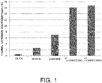
- Fig. 1 is a graph of thermal expansion coefficients of various materials in comparison. The thermal expansion of the piezoelectric single crystal is reduced by bonding the material having a small expansion coefficient, and hence the temperature characteristics are improved (e.g. see Non Patent Document 1) .
- a stack of a thin piezoelectric single crystal film on a support substrate causes noise referred to as spuriousness or ripples in an antiresonance frequency band.
- the noise is caused due to reflection from the interface between the piezoelectric single crystal film and the support substrate.
- Fig. 2 shows an exemplary spectrum at the reflection coefficient (S11) of a resonator prepared using a composite substrate having a stack of an LT film in 20 ⁇ m thickness on a silicon substrate.
- the difference between the peak and bottom of the spectrum is defined as spurious intensity (amplitude).
- Non Patent Document 2 discloses a method in which the bonding surface of LT is roughened with a #1000 grinding wheel to obtain a roughness of 300 nm in the arithmetic average roughness (Ra) and then the LT is bonded to a support substrate through an adhesive.
- the Lt is bonded to the substrate using an organic adhesive, resulting in a problem of the viewpoint of reliability.
- a plurality of processes is scheduled in which the substrate surface is patterned, the substrate is diced, and chips are mounted on devices.
- heating processes at temperatures of 250 to 400°C are repeated.
- organic substances made up of the adhesive are altered, resulting in a problem that a piezoelectric crystal film on the bonded substrate is peeled or cracked.
- an intermediate layer made of an inorganic material is formed on a piezoelectric single crystal substrate formed with an irregular structure and a support substrate is joined such that this intermediate layer is sandwiched.
- inorganic materials that are used as an intermediate layer include SiO x (1.5 ⁇ x ⁇ 2.5), Al 2 O 3 , AlN, SiN, SiON, and Ta 2 O 5 , for example.
- Representative examples of methods for forming this intermediate layer include chemical vapor deposition (CVD) and physical vapor deposition (PVD) represented by sputtering, for example.
- CVD chemical vapor deposition
- PVD physical vapor deposition
- a method can also be adopted in which a solution of an organic silicon compound is applied on a wafer and the solution is hardened by heat treatment to form an SiO 2 film.
- piezoelectric single crystals such as LT and LN
- LT and LN have the upper limit temperature referred to as a Curie temperature at which polarization is destroyed, and can not be heated to higher temperature to maintain the polarization state.
- LT has its Curie temperature near 600°C. It is extremely difficult to fully eliminate out gases even if processing is carried out below this temperature, and it is difficult to attain long-term reliability.
- SiO 2 that is an inorganic material used for an intermediate layer and a piezoelectric crystal, such as LT and LN, have a great difference in their thermal expansion coefficients.
- the thermal expansion coefficient of LT and LN is about 16 ppm, and the thermal expansion coefficient of SiO 2 is about 0.5 ppm. This difference causes cracks after high temperature treatment, and the subsequent processes can not be performed.
- Fig. 3 shows results of out gas analysis on samples in which an inorganic layer simulating an intermediate layer were prepared by three different methods.
- the first one is an analysis result of thermal desorption spectrometry (TDS) in which SiO 2 was deposited in a thickness of 5 ⁇ m on an LT single crystal substrate by CVD and then heat treatment was applied from at ambient temperature to a temperature of 1,000°C. From this result, the peak of the out gas is at near a temperature of 500°C. However, after that, it is shown that gases are continuously generated until the temperature reaches a temperature of 1,000°C.
- TDS thermal desorption spectrometry
- the peak of the out gas is at near a temperature of 500°C, degassing is continued even at a temperature of 600°C or more, and gases are continuously generated even at a temperature of 1,000°C.
- the third one is a TDS analysis result in which SiO 2 was deposited in a thickness of 5 ⁇ m by PVD and then similar heat treatment was applied.
- the peak of the out gas is at near a temperature of 500°C and degassing is continued even at a temperature of 600°C or more and continued until the temperature reaches a temperature of 1,000°C.
- the intermediate layers deposited by these methods have to be subjected to heat treatment at a temperature of 1,000°C or more for degassing.
- Patent Document 1 discloses a composite substrate, wherein an LT substrate having a room temperature CVD deposited SiO 2 layer thereon is bonded to a Si substrate having a 0.3 ⁇ m thick SiO 2 layer and a further 50 nm thick amorphous Si layer thereon (Example 4).
- Patent Document 2 an LT substrate having a silicon oxide film deposited thereon is bonded to a Si substrate having a silicon oxide film thereon, the latter film being formed by thermal oxidation, for example.
- An object is to provide a composite substrate having a piezoelectric single crystal layer bonded to a support substrate using an inorganic material as an intermediate layer in which peeling hardly occurs even though heating and cooling are repeated in processes after bonding.
- the intermediate layer is a film formed of an inorganic material, and at least a part of the film is thermally synthesized silica.
- thermally oxidized silica or thermally synthesized silica such as a synthetic silica sintered body, has the properties that can absorb gasses to some extent. At least a part of the intermediate layer is thermally synthesized silica like the above configuration, and thermally synthesized silica absorbs an out gas possibly generated in heating and cooling in the post-processes even though the rest of the intermediate layer is an inorganic material that insufficiently degases the out gas. Thus, peeling can hardly occur.
- the intermediate layer is constituted by at least two layers along a bonding surface of the composite substrate.
- a first intermediate layer in contact with the support substrate is a layer including the thermally synthesized silica.
- the layer of the intermediate layer in contact with the support substrate can be formed by deposition of thermally synthesized silica.
- the intermediate layer on the piezoelectric single crystal substrate side is an inorganic material that can be formed by deposition at a temperature lower than the Curie temperature.
- a material of the support substrate may be a silicon substrate.
- the thermally synthesized silica may be synthesized by thermal oxidation of the silicon substrate.
- the thermal oxidation layer is formed on the surface of the silicon substrate, and can be used as a part of the intermediate layer. Thermally synthesized silica can be easily formed.
- thermally synthesized silica may be a sintered body of synthetic silica.
- a heat resistant substrate such as sapphire, silicon nitride, aluminum nitride, silicon carbide or quartz glass
- Silica that is deposited on the support substrate by a given method is heated together with the support substrate, sintered silica is formed on the surface of the support substrate, and the sintered silica can be used as a part of the intermediate layer.
- a deposition method of silica may be chemical vapor deposition (CVD), physical vapor deposition (PVD), and applying and baking of a solution of an organic silicon compound, for example.
- CVD chemical vapor deposition
- PVD physical vapor deposition
- sintering may be performed by heat treatment at a temperature of around 1,000°C.
- a material of a second intermediate layer provided on the piezoelectric single crystal substrate side of a first intermediate layer in contact with the support substrate may include at least one of SiO x ,
- Al 2 O 3 , AlN, SiN, SiON, and Ta 2 O 5 are preferable because the substances can be deposited and processed by CVD and PVD, for example, at a temperature of 500°C or less that is relatively low temperature.
- the second intermediate layer may have at least two layers having different materials.
- the at least two layers may be layers of materials having different thermal expansion coefficients.
- a thickness of the first intermediate layer may be 20 nm or more. With this configuration, the first intermediate layer can be provided with a sufficient out gas absorption capability.
- a thickness of the second intermediate layer may be 25 ⁇ m or less. With this configuration, cracks can be prevented from being generated in the piezoelectric single crystal substrate caused by stress due to the difference in the thermal expansion coefficient between the piezoelectric single crystal substrate and the second intermediate layer. Note that there is no constraint specifically on the lower limit of the thickness of the second intermediate layer. In the case in which the interface to the piezoelectric single crystal substrate is flat, the thickness may be 50 nm or more. In the case in which the interface has an irregular structure, the projections of the piezoelectric single crystal substrate may be accommodated in the second intermediate layer.
- a thermally synthesized silica layer may be further provided on a back surface of the support substrate (i.e., the surface on the opposite side of the surface joined to the piezoelectric single crystal as the intermediate layer is sandwiched).
- the thermally synthesized silica layer is formed on both sides of the support substrate, the stress applied to the support substrate achieves a balance, and the warpage of the substrate is mitigated.
- the first intermediate layer is joined to the second intermediate layer by a third intermediate layer formed of amorphous silicon that is sandwiched between the first intermediate layer and the second intermediate layer.
- the thickness of the third intermediate layer is 50 nm or less. With this configuration, an out gas generated on the second intermediate layer side can be excellently transmitted on the first intermediate layer side.
- a thickness of the intermediate layer may be 8 ⁇ m or less. With this configuration, the heat resistance of the composite substrate can be improved. (12) More preferably, the thickness of the intermediate layer may be 7 ⁇ m or less. With this configuration, the heat resistance of the composite substrate can be further improved.
- a thickness of the piezoelectric single crystal may be 20 ⁇ m or less. With this configuration, with this configuration, the heat resistance of the composite substrate can be improved.
- an interface between the piezoelectric single crystal and the intermediate layer may have an irregular structure.
- a surface acoustic wave device may be configured including any one of the composite substrates of the present invention. With this configuration, a small-sized surface acoustic wave device of high performance can be implemented.
- a thickness of the piezoelectric single crystal may be 1.0 times or more and 3.5 times or less of a wavelength of a surface acoustic wave.
- a method for manufacturing a composite substrate according to the present invention includes the steps of: forming a first intermediate layer including thermally synthesized silica on a surface of a support substrate; forming a second intermediate layer including an inorganic material on a surface of a piezoelectric single crystal substrate; flattening a surface of the second intermediate layer; and bonding a surface of the first intermediate layer to the flattened surface of the second intermediate layer using a further layer of amorphous silicon, according to independent claim 9.
- the first intermediate layer that is a part of the intermediate layer includes thermally synthesized silica by the manufacturing method, the first intermediate layer can absorb an out gas possibly generated from the second intermediate layer in heating and cooling in the post-processes. Thus, peeling can hardly occur in the bonded substrates.
- the step of flattening the surface of the first intermediate layer may be further included. With this configuration, even in the case in which the surface of the first intermediate layer obtained by forming thermally synthesized silica is not flat, firm bonding can be implemented. Note that the step of flattening the surface of the first intermediate layer is performed prior to the step of bonding.
- the step of forming irregularities on the surface of the piezoelectric single crystal substrate may be further included.
- the properties of a device prepared from the composite substrate obtained by the manufacturing method can be made excellent. Specifically, for example, the spurious phenomenon of the resonator prepared from the composite substrate obtained by the manufacturing method can be suppressed.
- the first intermediate layer may be thermally synthesized silica in which a silica layer deposited by chemical vapor deposition (CVD) is sintered at a temperature of 800°C or more.
- CVD chemical vapor deposition
- the first intermediate layer may be thermally synthesized silica in which a silica layer deposited by physical vapor deposition (PVD) is sintered at a temperature of 800°C or more.
- PVD physical vapor deposition
- the first intermediate layer may be a layer of thermally synthesized silica in which a solution of an organic silicon compound is applied and sintered at a temperature of 800°C or more.
- the silica layer is sintered at a temperature of 800°C or more.
- the degassing of the silica layer is promoted, and a sintered, fine thermally synthesized silica (sintered silica) film can be formed.
- the thermally synthesized silica has excellent absorption capability.
- the temperature in sintering may be preferably a temperature of 1,000°C or more.
- a material of the support substrate may be selected from silicon, sapphire, silicon carbide, silicon nitride, aluminum nitride, and silica glass.
- the silica layer can be sintered at a high temperature of 800°C or more in the methods of (20) to (22).
- the first intermediate layer may be formed by thermal oxidation of the support substrate. With this configuration, the thermal oxidation layer is formed on the surface of the silicon substrate, and can be used as a part of the intermediate layer. In addition, thermally synthesized silica can be easily formed.
- the step of heating the second intermediate layer at a highest temperature lower than a Curie temperature of the piezoelectric single crystal may be further included.
- a temperature when the second intermediate layer is heated may be preferably a temperature of 600°C or less.
- a thermally synthesized silica layer having a material the same as a material of the first intermediate layer may also be formed on a back surface of the support substrate (i.e., the surface on the opposite side of the surface joined to the piezoelectric single crystal as the intermediate layer is sandwiched).
- the thermally synthesized silica layer is formed on both sides of the support substrate, stress applied to the support substrate achieves a balance, and hence the warpage of the substrate can be mitigated.
- the thermally synthesized silica layer on the back surface of the support substrate may be appropriately removed using hydrofluoric acid, for example.
- an amorphous silicon layer is further deposited on at least one of the surface of the first intermediate layer and the surface of the second intermediate layer, and then the first intermediate layer is bonded to the second intermediate layer.
- the joining strength can be improved, and cracks or peeling can hardly occur.
- a total thickness of the amorphous silicon layer is 50 nm or less. With this configuration, an out gas generated on the second intermediate layer side can be excellently transmitted on the first intermediate layer side.
- an activation process may be applied to at least one surface of the first intermediate layer and the second intermediate layer, and then the surface of the first intermediate layer may be bonded to the surface of the second intermediate layer.
- the surface activation process may be any one of ozone water treatment, UV ozone treatment, ion beam treatment, and plasma treatment. By the surface activation process, firm bonding can be implemented.
- the surface of the first intermediate layer and/or the surface of the second intermediate layer may be flattened by chemical-mechanical polishing.
- a material of the second intermediate layer may include any one of SiO x , Al 2 O 3 , AlN, SiN, SiON, and Ta 2 O 5 .
- the above-mentioned substances are preferable because the substances can be deposited and processed by CVD and PVD, for example, at a temperature of 500°C or less that is relatively low temperature.
- the second intermediate layer may be formed by chemical vapor deposition (CVD).
- the second intermediate layer may be formed by physical vapor deposition (PVD).
- the second intermediate layer may be formed in which a solution of an organic silicon compound is applied and the applied organic silicon compound is hardened.
- a step of performing a process of ion implantation into the piezoelectric single crystal substrate may be included prior to the step of bonding, and peeling may be performed at an interface in a region in which the ions are implanted after the step of bonding.
- hydrogen ions may be implanted in an amount of 6.0 ⁇ 10 16 atoms/cm 2 to 2.75 ⁇ 10 17 atoms/cm 2 .
- hydrogen molecule ions may be implanted in an amount of 3.0 ⁇ 10 16 atoms/cm 2 to 1.37 ⁇ 10 17 atoms/cm 2 .
- step of peeling mechanical peeling may be performed along a region in which the ions are implanted. (41) Alternatively, in the step of peeling, peeling may be performed using a flash lamp annealing.
- a step of grinding and/or polishing the piezoelectric single crystal substrate to reduce a thickness may be included after the step of bonding.
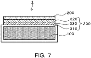
- a composite substrate 1 according to an embodiment is manufactured through processes in which a support substrate 100 and a piezoelectric single crystal substrate 200 are processed before bonding and then these two substrates are bonded to each other. In the following, manufacturing methods will be described with reference to Figs. 4 to 6 .
- the support substrate 100 is prepared ( Fig. 4(a) ).
- the support substrate 100 is selected from silicon, sapphire, silicon carbide, silicon nitride, aluminum nitride, and silica glass.
- a first intermediate layer 310 including thermally synthesized silica is formed on the surface of the support substrate 100 ( Fig. 4(b) ).
- a thermally synthesized silica layer having the same material as the first intermediate layer 310 may be formed on the back surface of the support substrate 100.
- the silica layer on the back surface may be appropriately removed using hydrofluoric acid, for example.
- a thermally oxidized silica film to be the first intermediate layer 310 can be formed by thermal oxidation of a silicon substrate. Since thermally oxidized silica is grown at high temperature, the thermally oxidized silica has the properties of being fine with few impurities and can absorb gases to some extent.
- the first intermediate layer 310 can be formed by methods below regardless of whether the material of the support substrate 100 is silicon or not. That is, the first intermediate layer 310 may be formed by sintering a silica layer deposited by chemical vapor deposition (CVD) at a temperature of 800°C or more. The first intermediate layer 310 may be formed by sintering a silica layer deposited by physical vapor deposition (PVD) at a temperature of 800°C or more. Alternatively, the first intermediate layer 310 may be formed in which a solution of an organic silicon compound is applied and then sintered at a temperature of 800°C or more. In the case in which the first intermediate layer 310 is formed in a silica sintered body, a heat resistant substrate is preferably used such that synthetic silica deposited on the support substrate 100 can be sintered together with the support substrate 100.
- CVD chemical vapor deposition
- PVD physical vapor deposition
- the surface of the first intermediate layer 310 is flattened as necessary ( Fig. 4(c) ).
- This flattening may be performed by chemical-mechanical polishing. Note that in the case in which a silicon substrate having a mirror-finished surface is used as the support substrate 100 and the first intermediate layer 310 is formed by thermal oxidation, the surface of the first intermediate layer 310 has a mirror surface similar to the base, and hence this flattening process is unnecessary.
- amorphous silicon is deposited, for example, on the surface of the first intermediate layer 310.
- Stacking amorphous silicon makes a bonding interface of Si/SiO 2 or Si/Si, and this provides joining strength slightly higher than SiO 2 /SiO 2 bonding (for details see Tong Q.Y. and Gosele U., Semiconductor Wafer Bonding, Science and Technology, Chapter 4.7.1, 1999 ).
- the thickness of the amorphous silicon to be deposited is 50 nm or less such that gas transmission is not inhibited.
- the surface of the first intermediate layer 310 may be subjected to activation.
- the surface activation process may be any one of ozone water treatment, UV ozone treatment, ion beam treatment, and plasma treatment, for example.
- the piezoelectric single crystal substrate 200 is prepared ( Fig. 5 (a) ).
- the piezoelectric single crystal substrate 200 is a piezoelectric single crystal, such as lithium tantalate (LT) and lithium niobate (LN).
- irregularities are formed on the surface of the piezoelectric single crystal substrate 200 as necessary ( Fig. 5 (b) ).
- the irregularities have the effect that suppresses the spurious phenomenon of a resonator prepared from the composite substrate 1. In the case in which the composite substrate 1 is used for the application that spuriousness causes no problem, this process may be omitted.
- a second intermediate layer 320 is formed by depositing the second intermediate layer 320 including an inorganic material on the surface of the piezoelectric single crystal substrate 200 ( Fig. 5 (c) ).
- the material of the second intermediate layer 320 includes any one of SiO x (e.g. SiO 2 ), Al 2 O 3 , AlN, SiN, SiON, and Ta 2 O 5 .
- the second intermediate layer 320 can be formed by methods below. That is, the second intermediate layer 320 may be deposited by chemical vapor deposition (CVD). The second intermediate layer may be deposited by physical vapor deposition (PVD). Alternatively, the second intermediate layer 320 may be deposited in which a solution of an organic silicon compound is applied and then hardened.
- the second intermediate layer 320 formed by any one of the methods may be heated at a temperature lower than the Curie temperature of the piezoelectric crystal.
- a heating temperature is preferably at a temperature of 600°C or less.
- the second intermediate layer 320 may be configured in which the layer 320 has at least two layers having different materials.
- the surface of the formed second intermediate layer 320 is flattened ( Fig. 5 (d) ).
- This flattening may be performed by chemical-mechanical polishing.
- amorphous silicon is deposited, for example, on the surface of the second intermediate layer 320.
- the thickness of the amorphous silicon to be deposited is 50 nm or less such that gas transmission is not inhibited. Note that in the case in which amorphous silicon is also deposited on the first intermediate layer 310, the total thickness is 50 nm or less.
- the surface of the second intermediate layer 320 may be subjected to activation.
- the surface activation process may be any one of ozone water treatment, UV ozone treatment, ion beam treatment, and plasma treatment, for example.
- the surface of the first intermediate layer 310 is bonded to the surface of the second intermediate layer 320 ( Fig. 6 (a) ).
- joining strength may be improved by heating the bonded substrates at a low temperature (e.g., 120°C).
- the piezoelectric single crystal substrate 200 is ground and polished to reduce the thickness.
- the thickness of the piezoelectric single crystal substrate 200 is reduced to a thickness of about 20 ⁇ m ( Fig. 6 (b) ).
- additional heat treatment is performed further as necessary, and joining force may be reinforced.
- the first intermediate layer 310 and the second intermediate layer 320 thus bonded and joined configure an intermediate layer 300.
- the first intermediate layer 310, the second intermediate layer 320, and the third intermediate layer 330 configure the intermediate layer 300, according to the present invention.
- the composite substrate 1 having the piezoelectric single crystal substrate 200 joined to the support substrate 100 with the intermediate layer 300 sandwiched can be manufactured.
- an aluminum (Al) thin film in a thickness of 0.4 ⁇ m was sputtered, electrodes were formed by photolithography, and then a four-stage rudder filter formed of a two-stage parallel resonators and a four-stage series resonator at a wavelength of 5 ⁇ m and a resonator were prepared.
- a g-line stepper was used, and for Al etching, a mixed gas of Cl 2 , BCl 3 , N 2 , and CF 4 was used.
- the reflection coefficient (S11) of the prepared four-stage rudder filter was measured. The difference between the peak and bottom of observed spuriousness was evaluated as spurious intensity.
- ⁇ is the angular frequency
- ⁇ is the group delay time.
- the Q-value is the value indicating the sharpness of the waveform of resonance, and a filter having a higher Q value can be of excellent properties with a small loss. Since the Q-value has frequency dependency, the maximum value (Q max ) of the Q-value was evaluated.
- An LT substrate in a diameter of 15.24 cm (six inches) having a roughness of about 230 nm (in P-V, about 1.7 ⁇ m) at Ra (arithmetic average roughness) was prepared as a piezoelectric single crystal substrate.
- an SiO 2 film was formed by deposition in a thickness of about 10 ⁇ m by plasma CVD using silane and oxygen gas as raw material gases. This SiO 2 film was subjected to heat treatment at a temperature of about 400°C, the surface was polished and mirror-finished, and the SiO 2 film was finished in a film thickness of about 2 ⁇ m.
- An Si substrate in a diameter of 15.24 cm (six inches) having a thermal oxidation film grown in a thickness of 500 nm was prepared as a support substrate. After that, plasma surface activation was applied to both of the LT substrate deposited with the SiO 2 film and the Si substrate having the thermal oxidation film grown. The two substrates were bonded to each other and subjected to heat treatment at a temperature of 120°C, and then the LT was ground and polished to reduce the thickness to about 20 ⁇ m. The cross section of a microphotograph of the composite substrate thus finished is shown in Fig. 8 .
- a heat resistance test was examined in which the wafer of the composite substrate was diced in two-millimeter squares and reciprocated between a hot plate at a temperature of 200°C and a metal cooling stage (the substrate was held for 30 seconds each on the hot plate and on the cooling stage). The wafer was reciprocated for 100 times. However, peeling, for example, was not observed.
- Example 1 An experiment similar to Example 1 was performed using an LT substrate provided with an SiO 2 film similarly to Example 1 and an Si substrate without thermal oxidation. As a result of a heat resistance test similar to Example 1, peeling was observed at edges in the fifth reciprocation. With the comparison between Example 1 and Comparative Example 1, the LT substrate provided with the SiO 2 film by plasma CVD was bonded to the Si substrate having the thermal oxidation film grown, and hence it was shown that peeling can be suppressed compared with the case in which the Si substrate with no thermal oxidation film grown is bonded.
- An LT substrate in a diameter of 15.24 cm (six inches) having a roughness of about 230 nm (in P-V, about 1.7 ⁇ m) in Ra was prepared.
- a process was repeated for a plurality of times in which a solution of an organic silicon compound was spin-coated and heated at a temperature of 350°C, and hence an SiO 2 layer in a thickness of about 5 ⁇ m was obtained.
- the solution of the organic silicon compound used here is two types of perhydropolysilazane (a solvent was dibutylether) and methyltrimethoxysilane (a solvent was propylene glycol monoethyl ether).
- a heat resistance test was examined in which the wafer of the composite substrate was diced in two-millimeter squares and reciprocated between a hot plate at a temperature of 200°C and a metal cooling stage (the substrate was held for 30 seconds each on the hot plate and on the cooling stage). The wafer was reciprocated for 100 times. However, peeling, for example, was not observed.
- Example 2 An experiment similar to Example 2 was performed using an LT substrate provided with an SiO 2 film similarly to Example 2 and an Si substrate without thermal oxidation. As a result of a heat resistance test similar to Example 2, peeling was observed at edges in the seventh reciprocation. With the comparison between Example 2 and Comparative Example 2, the LT substrate provided with the SiO 2 film by spin-coating and heating the solution of the organic silicon compound was bonded to the Si substrate having the thermal oxidation film grown, and hence it was shown that peeling can be suppressed compared with the case in which the Si substrate with no thermal oxidation film grown is bonded.
- An LT substrate in a diameter of 15.24 cm (six inches) having a roughness of about 230 nm (in P-V, about 1.7 ⁇ m) in Ra was prepared.
- an SiO 2 film was deposited in a thickness of about 10 ⁇ m by PVD (here, magnetron sputtering). After heat treatment at a temperature of about 400°C, the surface of this SiO 2 film was polished and mirror-finished.
- An Si substrate in a diameter of 15.24 cm (six inches) having a thermal oxidation film grown in a thickness of 500 nm was prepared. Plasma surface activation was applied to the two substrates. The two substrates were bonded to each other and subjected to heat treatment at a temperature of 120°C, the LT was ground and polished to reduce the thickness to 20 ⁇ m, and then a composite substrate was obtained.
- a heat resistance test was examined in which the wafer of the composite substrate was diced in two-millimeter squares and reciprocated between a hot plate at a temperature of 200°C and a metal cooling stage (the substrate was held for 30 seconds each on the hot plate and on the cooling stage). The wafer was reciprocated for 100 times. However, peeling, for example, was not observed.
- Example 3 An experiment similar to Example 3 was performed using an LT substrate provided with an SiO 2 film similarly to Example 3 and an Si substrate without thermal oxidation. As a result of a heat resistance test similar to Example 3, peeling was observed at edges in the second reciprocation. With the comparison between Example 3 and Comparative Example 3, the LT substrate provided with the SiO 2 film by PVD was bonded to the Si substrate having the thermal oxidation film grown, and hence it was shown that peeling can be suppressed compared with the case in which the Si substrate with no thermal oxidation film grown is bonded.
- a plurality of LT substrates in a diameter of 15.24 cm (six inches) having a roughness of about 230 nm (in P-V, about 1.7 ⁇ m) in Ra was prepared.
- an SiO 2 film was deposited in a thickness of about 10 ⁇ m by plasma CVD.
- Heat treatment at a temperature of about 400°C was applied to the SiO 2 film, the surface was polished and mirror-finished, and then amorphous silicon (a-Si) was deposited in various thicknesses as shown in Table 1.
- the amorphous silicon was deposited by varying thicknesses by PVD (magnetron sputtering) and by CVD.
- Plasma surface activation was applied to both of the LT substrate and the Si substrate in a diameter of 15.24 cm (six inches) having the thermal oxidation film grown in a thickness of 500 nm.
- the two substrates were bonded to each other and subjected to heat treatment at a temperature of 120°C, the LT was ground and polished to reduce the thickness to 20 ⁇ m, and then a composite substrate was obtained.
- Amorphous silicon was deposited on the side of an Si substrate having a thermal oxidation film grown, not on the LT substrate side, and an experiment similar to Example 4 was performed. The result was almost the same as the result in Example 4. From the result, it was shown that amorphous silicon can be provided on any of the LT substrate side and the Si substrate side.
- Amorphous silicon was deposited on both of an LT substrate and an oxidation Si substrate side, and an experiment similar to Example 4 was performed.
- the thickness of the amorphous silicon was the total thickness of the amorphous silicon films deposited on both substrates. The result was almost the same as the result in Example 4. From the result, it was shown that amorphous silicon can be provided on both of the LT substrate side and the Si substrate side.
- the experiment was performed as the surface activation method was changed to ozone water treatment, UV ozone treatment, and ion beam treatment. However, no difference was found in the results of bonding. It is thought that the present invention does not strongly depend on activation methods. No great difference was observed when surface activation was applied to only one substrate.
- a four-stage rudder filter was formed on a composite substrate prepared by the method in Example 1, the spectrum of the reflection coefficient (S11) was measured, and the spurious properties were evaluated. As a result, as shown in Fig. 9 , it was confirmed that spurious strength is 1 dB or less. It was revealed that the resonator prepared by this method can effectively reduce spuriousness.
- Example 2 An experiment similar to Example 1 was performed by changing the thickness of a thermal oxidation film grown on an Si substrate. As a result, an effect was confirmed in the thermal oxidation films in a thickness of 20 nm or more. However, in thermal oxidation films in a thickness of less than 20 nm, out gas absorption capability was insufficient, and peeling was sometimes observed in heating and cooling cycle tests.
- Example 2 An experiment similar to Example 1 was performed by changing the thickness of an SiO 2 film deposited on an LT substrate. The result is shown in Table 2.
- the thickness of the deposited SiO 2 shown in Table 2 is the thickness after the surface was flattened. This result revealed that when the thickness of the SiO 2 film (only the deposited film, the thermal oxidation film is not included) exceeds 25 ⁇ m, cracks were generated in the LT layer. It is thought that the cracks were generated by stress due to the difference in the expansion coefficient between LT and SiO 2 . In the case in which the thickness of SiO 2 is 25 ⁇ m or less, SiO 2 can be deformed following the difference in the expansion coefficient to some extent.
- An LT substrate in a diameter of 15.24 cm (six inches) having a mirror-finished surface on one side was prepared.
- an Al 2 O 3 film was deposited in a thickness of 1 ⁇ m by sputtering.
- an SiO 2 film was deposited in a thickness of about 10 ⁇ m by plasma CVD using silane and oxygen gas as raw material gases.
- the film stack of Al 2 O 3 and SiO 2 was subjected to heat treatment at a temperature of about 400°C, the surface was polished and mirror-finished, and the SiO 2 film was finished in a film thickness of about 2 ⁇ m.
- An Si substrate in a diameter of 15.24 cm (six inches) having a thermal oxidation film grown in a thickness of 500 nm was prepared.
- Plasma surface activation was applied to the two substrates.
- the two substrates were bonded to each other and subjected to heat treatment at a temperature of 120°C, the LT was ground and polished to reduce the thickness to about 6 ⁇ m, and then a composite substrate was obtained.
- a heat resistance test was examined in which the wafer of the composite substrate was diced in two-millimeter squares and reciprocated between a hot plate at a temperature of 200°C and a metal cooling stage (the substrate was held for 30 seconds each on the hot plate and on the cooling stage). The wafer was reciprocated up to 200 reciprocations. However, peeling, for example, was not observed. From the example, it was shown that a multilayered intermediate layer (i.e., the second intermediate layer) may be provided on the LT substrate side before bonding.
- the second intermediate layer may be provided on the LT substrate side before bonding.
- An LT substrate in a diameter of 15.24 cm (six inches) having a roughness of about 230 nm (in P-V, about 1.7 ⁇ m) at Ra (arithmetic average roughness) was prepared.
- an SiO 2 film was formed by deposition in a thickness of about 10 ⁇ m by plasma CVD using silane and oxygen gas as raw material gases. This SiO 2 film was subjected to heat treatment at a temperature of about 400°C, the surface was polished and mirror-finished, and the SiO 2 film was finished in a film thickness of about 2 ⁇ m.
- a sapphire substrate in a diameter of 15.24 cm (six inches) was prepared, and on the substrate, an SiO 2 film was deposited in a thickness of about 5 ⁇ m by plasma CVD.
- the SiO 2 film on the sapphire substrate was sintered by heat treatment at a temperature of 800°C, the surface was polished and mirror-finished, and the SiO 2 film was finished in a film thickness of 1 ⁇ m.
- a plasma activation process was applied to both of the SiO 2 film deposited on the LT substrate and the sintered SiO 2 film deposited on the sapphire substrate, the two substrates were bonded to each other and subjected to heat treatment at a temperature of 120°C, the LT was ground and polished to reduce the thickness to 20 ⁇ m, and then a composite substrate was obtained.
- a heat resistance test was examined in which the wafer of the composite substrate was diced in two-millimeter squares and reciprocated between a hot plate at a temperature of 200°C and a metal cooling stage (the substrate was held for 30 seconds each on the hot plate and on the cooling stage). The wafer was reciprocated for 100 times. However, peeling, for example, was not observed. From the example, it was shown that a sapphire substrate can be used as a support substrate. It was shown that thermally synthesized silica obtained by heating and sintering SiO 2 deposited by CVD can be used for an intermediate layer (i.e., the first intermediate layer) provided on the support substrate side before bonding.
- An LT substrate in a diameter of 15.24 cm (six inches) having a roughness of about 230 nm (in P-V, about 1.7 ⁇ m) at Ra (arithmetic average roughness) was prepared.
- an SiO 2 film was formed by deposition in a thickness of about 10 ⁇ m by plasma CVD using silane and oxygen gas as raw material gases. This SiO 2 film was subjected to heat treatment at a temperature of about 400°C, the surface was polished and mirror-finished, and the SiO 2 film was finished in a film thickness of about 2 ⁇ m.
- a sapphire substrate in a diameter of 15.24 cm (six inches) was prepared, and on the substrate, an SiO 2 film was deposited in a thickness of about 10 ⁇ m by PVD (magnetron sputtering).
- the SiO 2 film on the sapphire substrate was sintered by heat treatment at a temperature of 900°C, the surface was polished and mirror-finished, and SiO 2 film was finished in a film thickness of 1 ⁇ m.
- a plasma activation process was applied to both of the SiO 2 film deposited on the LT substrate and the sintered SiO 2 film deposited on the sapphire substrate, the two substrates were bonded to each other and subjected to heat treatment at a temperature of 120°C, the LT was ground and polished to reduce the thickness to 20 ⁇ m, and then a composite substrate was obtained.
- a heat resistance test was examined in which the wafer of the composite substrate was diced in two-millimeter squares and reciprocated between a hot plate at a temperature of 200°C and a metal cooling stage (the substrate was held for 30 seconds each on the hot plate and on the cooling stage). The wafer was reciprocated for 100 times. However, peeling, for example, was not observed. From the example, it was shown that a sapphire substrate can be used as a support substrate. It was shown that thermally synthesized silica obtained by heating and sintering SiO 2 deposited by PVD can be used for an intermediate layer (i.e., the first intermediate layer) provided on the support substrate side before bonding.
- An LT substrate in a diameter of 15.24 cm (six inches) having a roughness of about 230 nm (in P-V, about 1.7 ⁇ m) at Ra (arithmetic average roughness) was prepared.
- an SiO 2 film was formed by deposition in a thickness of about 10 ⁇ m by plasma CVD using silane and oxygen gas as raw material gases. This SiO 2 film was subjected to heat treatment at a temperature of about 400°C, the surface was polished and mirror-finished, and the SiO 2 film was finished in a film thickness of about 2 ⁇ m.
- a sapphire substrate in a diameter of 15.24 cm (six inches) was prepared, and on the substrate, an SiO 2 film was deposited in a thickness of about 3 ⁇ m by repeating a process of spin coating a solution of the organic silicon compound (a dibutylether solution of perhydropolysilazane) and a process of thermosetting at a temperature of 350°C for a few times.
- the SiO 2 film on the sapphire substrate was sintered by heat treatment at a temperature of 900°C, the surface was polished and mirror-finished, and the thickness of the SiO 2 film was finished to a film thickness of 0.5 ⁇ m.
- a plasma activation process was applied to both of the SiO 2 film deposited on the LT substrate and the sintered SiO 2 film deposited on the sapphire substrate, the two substrates were bonded to each other and subjected to heat treatment at a temperature of 120°C, the LT was ground and polished to reduce the thickness to 20 ⁇ m, and then a composite substrate was obtained.
- a heat resistance test was examined in which the wafer of the composite substrate was diced in two-millimeter squares and reciprocated between a hot plate at a temperature of 200°C and a metal cooling stage (the substrate was held for 30 seconds each on the hot plate and on the cooling stage). The wafer was reciprocated for 100 times. However, peeling, for example, was not observed. From the example, it was shown that a sapphire substrate can be used as a support substrate. It was shown that thermally synthesized silica obtained by applying, heating, and sintering organic silicon can be used for an intermediate layer (i.e., the first intermediate layer) provided on the support substrate side before bonding.
- An LT substrate in a diameter of 15.24 cm (six inches) having a roughness of about 230 nm (in P-V, about 1.7 ⁇ m) at Ra (arithmetic average roughness) was prepared.
- an SiO 2 film was formed by deposition in a thickness of about 10 ⁇ m by plasma CVD using silane and oxygen gas as raw material gases. This SiO 2 film was subjected to heat treatment at a temperature of about 400°C, the surface was polished and mirror-finished, and the SiO 2 film was finished in a film thickness of about 2 ⁇ m.
- a silica glass substrate in a diameter of 15.24 cm (six inches) was prepared, and on the substrate, an SiO 2 film was deposited in a thickness of about 3 ⁇ m by repeating a process of spin coating a solution of the organic silicon compound (a propylene glycol monoethyl ether solution of methyltrimethoxysilane) and a process of thermosetting at a temperature of 350°C for a few times.
- the SiO 2 film on the silica glass substrate was sintered by heat treatment at a temperature of 1,000°C, the surface was polished and mirror-finished, and the thickness of the SiO 2 film was finished to a film thickness of 0.5 ⁇ m.
- a plasma activation process was applied to both of the SiO 2 film deposited on the LT substrate and the sintered SiO 2 film deposited on the silica glass substrate, the two substrates were bonded to each other and subjected to heat treatment at a temperature of 120°C, the LT was ground and polished to reduce the thickness to 20 ⁇ m, and then a composite substrate was obtained.
- a heat resistance test was examined in which the wafer of the composite substrate was diced in two-millimeter squares and reciprocated between a hot plate at a temperature of 200°C and a metal cooling stage (the substrate was held for 30 seconds each on the hot plate and on the cooling stage). The wafer was reciprocated for 100 times. However, peeling, for example, was not observed. From the example, it was shown that a silica glass substrate can be used as a support substrate. It was shown that thermally synthesized silica obtained by applying, heating, and sintering organic silicon can be used for an intermediate layer (i.e., the first intermediate layer) provided on the support substrate side before bonding.
- the irregular structure of the LT substrate was formed by polishing using free abrasive grains.
- the definitions of Ra and RSm were in compliance with JIS B 0601:2001 and ISO 4287:1997, and calculated from the profiles measured using an atomic force microscope (AFM).
- SiO 2 was deposited in a thickness of about 10 ⁇ m at a temperature of 35°C using plasma CVD, the surface having SiO 2 deposited was polished to form a mirror surface. At this time, the polishing amount was changed depending on the LT substrates, and the thickness of SiO 2 was from 1.5 ⁇ m to 9.5 ⁇ m.
- An Si substrate to be a support substrate was subjected to heat treatment at a temperature of 850°C in an oxygen atmosphere, and hence thermally oxidized silica in a thickness of 0.5 ⁇ m was formed on the surface of the Si substrate.
- Thermally oxidized silica formed on both of the SiO 2 mirror surface and the surface of the Si substrate was subjected to plasma surface activation, the LT substrate was bonded to the support substrate, the LT substrate was polished, and then a composite substrate was prepared. At this time, the polishing amount was changed depending on the substrates, and the thickness of the LT substrate was 5 ⁇ m to 25 ⁇ m.
- an LT substrate in a thickness of 15 ⁇ m or less is usable regardless of an intermediate layer in a thickness of 2 to 10 ⁇ m, which is preferable.
- the total thickness of the intermediate layer is preferably 9 ⁇ m or less.
- the total thickness of the intermediate layer is preferably 8 ⁇ m or less.
- the thickness of the LT substrate when the thickness of the LT substrate is 15 ⁇ m or less, the thickness of the intermediate layer is 7 ⁇ m or less, which is more preferable.
- the thickness of the intermediate layer is 6 ⁇ m or less, which is more preferable.
- the Q-value is more increased.
- the Q-value tend to decrease.
- the spurious intensity is suppressed as low as 1.0 dB or less.
- An LT substrate in a diameter of 100 mm and a thickness of 0.35 mm having a roughness of 20 nm in Ra (arithmetic average roughness) was prepared.
- a 200 nm SiO 2 film was deposited in a thickness of about 10 ⁇ m film by PVD, the film was polished to a thickness of 50 nm, the surface was mirror-finished. It was confirmed that the surface roughness was 1.0 nm or less in RMS.
- hydrogen ions H +
- the dose amount was 7. 0 ⁇ 10 16 atoms/cm 2 and the accelerating voltage was 100 KeV.
- An Si substrate is prepared as a support substrate, and the thermal oxidation film in a thickness of 500 nm was grown.
- a plasma activation process was applied to the LT substrate and the Si substrate, and surface activation was performed.
- the two substrates were bonded to each other, and subjected to heat treatment at a temperature of 100°C for 24 hours.
- mechanical peeling was performed in which a blade in a wedge shaped was placed near the ion implantation interface on the side surface of the substrates thus bonded to each other.
- a composite substrate having a stack of the LT thin film in a thickness of about 600 nm on the Si substrate through the SiO 2 layer can be obtained.
- polishing to provide a mirror surface evaluation was performed. However, in a thermal endurance test, peeling was not observed.
- Example 17 the implantation of hydrogen ions to the LT substrate can also be performed before the SiO 2 film is deposited. Also with this configuration, the effect similar to the case can be obtained in which the SiO 2 film was deposited and then hydrogen ions were implanted.
- the dose amount of hydrogen ions ranges from 6.0 ⁇ 10 16 atoms/cm 2 to 2.75 ⁇ 10 17 atoms/cm 2
- the similar effect can be obtained.
- the similar effect can be obtained by implanting hydrogen molecule ions (H 2 + ) in the range of 3.0 ⁇ 10 16 atoms/cm 2 to 1.37 ⁇ 10 17 atoms/cm 2 .
- An LT substrate in a diameter of 100 mm and a thickness of 0.35 mm having a roughness of 20 nm in Ra (arithmetic average roughness) was prepared.
- a 200 nm SiO 2 film was deposited in a thickness of about 10 ⁇ m film by PVD, the film was polished to a thickness of 50 nm, the surface was mirror-finished. It was confirmed that the surface roughness was 1.0 nm or less in RMS.
- hydrogen ions were implanted under in which the dose amount was 7.0 ⁇ 10 16 atoms/cm 2 and the accelerating voltage was 100 KeV.
- An Si substrate is prepared as a support substrate, and the thermal oxidation film in a thickness of 500 nm was grown.
- a plasma activation process was applied to the LT substrate and the Si substrate, and surface activation was performed.
- the two substrates were bonded to each other, and subjected to heat treatment at a temperature of 100°C for 24 hours.
- peeling was performed at the ion implantation interface in which flash light was irradiated to the bonded substrates from the LT side using a flash lamp annealing (FLA) device.
- FLA flash lamp annealing
- Example 18 the implantation of hydrogen ions to the LT substrate can also be performed before the SiO 2 film is deposited. Also with this configuration, the effect similar to the case can be obtained in which the SiO 2 film was deposited and then hydrogen ions were implanted.
- the dose amount of hydrogen ions ranges from 6.0 ⁇ 10 16 atoms/cm 2 to 2.75 ⁇ 10 17 atoms/cm 2
- the similar effect can be obtained.
- the similar effect can be obtained by implanting hydrogen molecule ions (H 2 + ) in the range of 3.0 ⁇ 10 16 atoms/cm 2 to 1.37 ⁇ 10 17 atoms/cm 2 .
- the LT substrate is used as a piezoelectric single crystal substrate.
- results in exactly the same tendency were obtained even using an LN substrate.
- the material of the second intermediate layer was changed from SiO 2 to SiO x , Al 2 O 3 , AlN, SiN, SiON, and Ta 2 O 5 , for example, other than SiO 2 , the similar results were obtained.
- SiO 2 was used for all the investigation. However, the effect was exactly the same even on materials that are not strictly stoichiometric like SiO 2 ⁇ 0.5 . It is considered that the effect is exerted by the intermediate layer mainly burying the irregularities.
- the material of the support substrate was changed to silicon, silicon carbide, silicon nitride, or aluminum nitride, a synthetic silica film was formed on the surface by CVD, PVD, or by applying organic silicon, the substrate was heated and sintered at a temperature of 800°C or more, and then thermally synthesized silica was formed, the substrates were able to be excellently joined to each other. The substrates were diced in two-millimeter squares for a temperature cycle test. However, no peeling was observed.
Landscapes
- Physics & Mathematics (AREA)
- Acoustics & Sound (AREA)
- Engineering & Computer Science (AREA)
- Manufacturing & Machinery (AREA)
- Chemical & Material Sciences (AREA)
- Organic Chemistry (AREA)
- Inorganic Chemistry (AREA)
- Materials Engineering (AREA)
- Surface Acoustic Wave Elements And Circuit Networks Thereof (AREA)
- Silicon Compounds (AREA)
- Physical Vapour Deposition (AREA)
- Chemical Vapour Deposition (AREA)
Claims (23)
- Substrat composite (1) comprenant :un substrat de monocristal piézoélectrique (200) ;un substrat de support (100) ; etune couche intermédiaire (300) fournie entre le substrat de monocristal piézoélectrique et le substrat de support, dans lequella couche intermédiaire est un film formé d'un matériau inorganique, et au moins une partie du film est de la silice thermiquement synthétisée,dans lequel la couche intermédiaire est constituée d'au moins deux couches incluant une première couche intermédiaire (310) et une seconde couche intermédiaire (320) le long d'une surface de liaison du substrat composite, et la première couche intermédiaire en contact avec le substrat de support est une couche incluant la silice thermiquement synthétisée,caractérisé en ce quela première couche intermédiaire est jointe à la seconde couche intermédiaire par une troisième couche intermédiaire (330) formée de silicium amorphe ayant une épaisseur de 50 nm ou inférieure qui est insérée entre la première couche intermédiaire et la seconde couche intermédiaire.
- Substrat composite selon la revendication 1, dans lequel le substrat de support est un substrat de silicium, et la silice thermiquement synthétisée est synthétisée par oxydation thermique du substrat de silicium.
- Substrat composite selon la revendication 1 ou 2, dans lequel la silice thermiquement synthétisée est un corps fritté de silice synthétique.
- Substrat composite selon l'une quelconque des revendications 1 à 3, dans lequel un matériau de la seconde couche intermédiaire fourni sur le côté du substrat de monocristal piézoélectrique inclut au moins un de SiOx, Al2O3, AlN, SiN, SiON, et Ta2O5.
- Substrat composite selon la revendication 4, dans lequel la seconde couche intermédiaire présente au moins deux couches présentant des matériaux différents.
- Substrat composite selon l'une quelconque des revendications 1 à 5, comprenant de plus une couche de silice thermiquement synthétisée sur une surface arrière du substrat de support.
- Substrat composite selon l'une quelconque des revendications 1 à 6, dans lequel une épaisseur du monocristal piézoélectrique est de 20 µm ou inférieure.
- Substrat composite selon l'une quelconque des revendications 1 à 7, dans lequel une interface entre le monocristal piézoélectrique et la couche intermédiaire présente une structure irrégulière.
- Procédé pour la fabrication d'un substrat composite (1) comprenant les étapes de :formation d'une première couche intermédiaire (310) incluant de la silice thermiquement synthétisée sur une surface d'un substrat de support (100) ;formation d'une seconde couche intermédiaire (320) incluant un matériau inorganique sur une surface d'un substrat de monocristal piézoélectrique (200) ;aplanissement d'une surface de la seconde couche intermédiaire ; etliaison d'une surface de la première couche intermédiaire à la surface aplanie de la seconde couche intermédiaire,caractérisé en ce queune couche de silice amorphe (330) ayant une épaisseur de 50 nm ou inférieure est de plus déposée sur au moins une de la surface de la première couche intermédiaire et la surface de la seconde couche intermédiaire, et la première couche intermédiaire est ensuite liée à la seconde couche intermédiaire.
- Procédé pour la fabrication d'un substrat composite selon la revendication 9, comprenant de plus une étape d'aplanissement de la surface de la première couche intermédiaire.
- Procédé pour la fabrication d'un substrat composite selon la revendication 9 ou 10, comprenant de plus une étape de formation d'irrégularités sur la surface du substrat de monocristal piézoélectrique.
- Procédé pour la fabrication d'un substrat composite selon l'une quelconque des revendications 9 à 11, dans lequel la première couche intermédiaire est l'une quelconque d'une couche de silice thermiquement synthétisée dans laquelle une couche de silice déposée par dépôt chimique en phase vapeur est frittée à une température de 800°C ou supérieure, d'une couche de silice thermiquement synthétisée dans laquelle une couche de silice déposée par dépôt physique en phase vapeur est frittée à une température de 800°C ou supérieure, et d'une couche de silice thermiquement synthétisée dans laquelle une solution d'un composé de silicium organique est appliquée et frittée à une température de 800°C ou supérieure.
- Procédé pour la fabrication d'un substrat composite selon l'une quelconque des revendications 9 à 11, dans lequel un matériau du substrat de support est le silicium, et la première couche intermédiaire est formée par oxydation thermique du substrat de support.
- Procédé pour la fabrication d'un substrat composite selon l'une quelconque des revendications 9 à 13, comprenant de plus une étape de chauffage de la seconde couche intermédiaire à la température la plus élevée inférieure à une température de Curie du monocristal piézoélectrique.
- Procédé pour la fabrication d'un substrat composite selon la revendication 14, dans lequel la température la plus élevée dans l'étape de chauffage de la seconde couche intermédiaire est une température de 600°C ou inférieure.
- Procédé pour la fabrication d'un substrat composite selon l'une quelconque des revendications 9 à 15, dans lequel un procédé d'activation est appliqué à au moins une surface de la première couche intermédiaire et la seconde couche intermédiaire, et la surface de la première couche intermédiaire est ensuite liée à la surface de la seconde couche intermédiaire.
- Procédé pour la fabrication d'un substrat composite selon l'une quelconque des revendications 9 à 16, dans lequel la surface de la première couche intermédiaire et/ou la surface de la seconde couche intermédiaire est aplanie par polissage mécanochimique.
- Procédé pour la fabrication d'un substrat composite selon l'une quelconque des revendications 9 à 17, dans lequel un matériau de la seconde couche intermédiaire inclut l'un quelconque de SiOx, Al2O3, AlN, SiN, SiON, et Ta2O5.
- Procédé pour la fabrication d'un substrat composite selon l'une quelconque des revendications 9 à 18, dans lequel la seconde couche intermédiaire est formée par l'un quelconque de dépôt chimique en phase vapeur, dépôt physique en phase vapeur, et un procédé dans lequel une solution d'un composé de silicium organique est appliquée et le composé de silicium organique appliqué est durci.
- Procédé pour la fabrication d'un substrat composite selon l'une quelconque des revendications 9 à 19, comprenant les étapes de :réalisation d'un procédé d'implantation d'ions dans le substrat de monocristal piézoélectrique avant l'étape de liaison ; etréalisation d'une exfoliation à une interface dans une région dans laquelle les ions sont implantés après l'étape de liaison.
- Procédé pour la fabrication d'un substrat composite selon la revendication 20, dans lequel dans l'étape de réalisation du procédé d'implantation d'ions, des ions hydrogène sont implantés dans une quantité de 6,0 × 10¹⁶ atomes/cm2 à 2,75 × 10¹⁷ atomes/cm2, ou des ions de molécule d'hydrogène sont implantés dans une quantité de 3,0 × 10¹⁶ atomes/cm2 à 1,37 × 10¹⁷ atomes/cm2.
- Procédé pour la fabrication d'un substrat composite selon la revendication 20 ou 21, dans lequel, dans l'étape d'exfoliation, une exfoliation mécanique le long de l'interface de la région dans laquelle les ions sont implantés ou une exfoliation en utilisant un recuit à lampe éclair est réalisée.
- Procédé pour la fabrication d'un substrat composite selon l'une quelconque des revendications 9 à 20, comprenant une étape de broyage et/ou polissage du substrat de monocristal piézoélectrique pour réduire une épaisseur après l'étape de liaison.
Applications Claiming Priority (3)
| Application Number | Priority Date | Filing Date | Title |
|---|---|---|---|
| JP2016220238 | 2016-11-11 | ||
| JP2017089666 | 2017-04-28 | ||
| PCT/JP2017/036707 WO2018088093A1 (fr) | 2016-11-11 | 2017-10-10 | Substrat composite, dispositif à ondes acoustiques de surface et procédé de fabrication de substrat composite |
Publications (3)
| Publication Number | Publication Date |
|---|---|
| EP3540941A1 EP3540941A1 (fr) | 2019-09-18 |
| EP3540941A4 EP3540941A4 (fr) | 2020-06-17 |
| EP3540941B1 true EP3540941B1 (fr) | 2022-09-07 |
Family
ID=62109526
Family Applications (1)
| Application Number | Title | Priority Date | Filing Date |
|---|---|---|---|
| EP17870478.9A Active EP3540941B1 (fr) | 2016-11-11 | 2017-10-10 | Substrat composite pour dispositifs à ondes acoustiques de surface et procédé de fabrication du substrat composite |
Country Status (7)
| Country | Link |
|---|---|
| US (2) | US11800805B2 (fr) |
| EP (1) | EP3540941B1 (fr) |
| JP (1) | JP6770089B2 (fr) |
| KR (1) | KR102433349B1 (fr) |
| CN (1) | CN109891747B (fr) |
| TW (1) | TWI776822B (fr) |
| WO (1) | WO2018088093A1 (fr) |
Families Citing this family (25)
| Publication number | Priority date | Publication date | Assignee | Title |
|---|---|---|---|---|
| US11095266B2 (en) * | 2016-10-07 | 2021-08-17 | Qorvo Us, Inc. | Slanted apodization for acoustic wave devices |
| JP7152711B2 (ja) * | 2018-06-20 | 2022-10-13 | 日本電産マシンツール株式会社 | 接合基板の製造方法及び接合基板 |
| DE112019002418B4 (de) | 2018-06-22 | 2022-06-15 | Ngk Insulators, Ltd. | Verbundener Körper und Elastikwellenelement |
| JP2020036212A (ja) * | 2018-08-30 | 2020-03-05 | 信越化学工業株式会社 | 複合基板および複合基板の製造方法 |
| TWI815970B (zh) * | 2018-11-09 | 2023-09-21 | 日商日本碍子股份有限公司 | 壓電性材料基板與支持基板的接合體、及其製造方法 |
| JP2020090420A (ja) * | 2018-12-07 | 2020-06-11 | 住友金属鉱山株式会社 | 黒鉛製またはセラミックス製の基板、基板の製造方法、炭化珪素の成膜方法および炭化珪素基板の製造方法 |
| WO2021002046A1 (fr) * | 2019-07-03 | 2021-01-07 | 日本碍子株式会社 | Corps lié, et élément à ondes élastiques |
| US11183987B2 (en) * | 2019-09-26 | 2021-11-23 | Avago Technologies International Sales Pte. Limited | Acoustic resonator device |
| CN114641933A (zh) * | 2019-11-06 | 2022-06-17 | 株式会社村田制作所 | 弹性波装置 |
| JP7271458B2 (ja) * | 2020-02-03 | 2023-05-11 | 信越化学工業株式会社 | 複合基板の製造方法 |
| JP7274442B2 (ja) * | 2020-04-02 | 2023-05-16 | 信越化学工業株式会社 | 複合基板およびその製造方法 |
| JP7262415B2 (ja) * | 2020-04-03 | 2023-04-21 | 信越化学工業株式会社 | 複合基板およびその製造方法 |
| CN113540339B (zh) * | 2020-04-21 | 2024-07-12 | 济南晶正电子科技有限公司 | 一种制备压电复合薄膜的方法及压电复合薄膜 |
| JP7336413B2 (ja) * | 2020-04-30 | 2023-08-31 | 信越化学工業株式会社 | 複合基板の製造方法および複合基板 |
| JP7402112B2 (ja) | 2020-05-08 | 2023-12-20 | 信越化学工業株式会社 | 圧電性単結晶膜を備えた複合基板の製造方法 |
| JP7262421B2 (ja) * | 2020-05-08 | 2023-04-21 | 信越化学工業株式会社 | 圧電体複合基板およびその製造方法 |
| CN111880124B (zh) * | 2020-07-10 | 2021-11-19 | 中国科学院上海微系统与信息技术研究所 | 一种高频可调节磁场探测器的制备方法 |
| KR102430218B1 (ko) * | 2020-10-20 | 2022-08-11 | 한국전자기술연구원 | AlN(질화알루미늄) 박막 증착 방법 |
| CN112382563A (zh) * | 2020-11-13 | 2021-02-19 | 济南晶正电子科技有限公司 | 离子注入薄膜晶圆剥离方法、单晶薄膜及电子元器件 |
| JP7290156B2 (ja) * | 2021-02-05 | 2023-06-13 | 信越半導体株式会社 | 窒化物半導体基板及びその製造方法 |
| JP7695335B2 (ja) * | 2021-02-19 | 2025-06-18 | 信越化学工業株式会社 | 複合ウェーハおよびその製造方法 |
| KR20230128099A (ko) * | 2021-02-19 | 2023-09-01 | 신에쓰 가가꾸 고교 가부시끼가이샤 | 복합 웨이퍼 및 그 제조 방법 |
| FR3130073B1 (fr) * | 2021-12-06 | 2024-09-06 | Commissariat Energie Atomique | Procédé de transfert d’une couche |
| CN117460388B (zh) * | 2023-12-25 | 2024-07-23 | 天通瑞宏科技有限公司 | 一种复合衬底及其制备方法 |
| JP2026045923A (ja) * | 2024-08-30 | 2026-03-13 | グローバルウェーハズ・ジャパン株式会社 | 複合基板の製造方法、複合基板、および弾性波デバイス |
Family Cites Families (20)
| Publication number | Priority date | Publication date | Assignee | Title |
|---|---|---|---|---|
| JP2001053579A (ja) * | 1999-06-02 | 2001-02-23 | Matsushita Electric Ind Co Ltd | 弾性表面波素子と移動体通信機器 |
| WO2003052840A1 (fr) | 2001-12-18 | 2003-06-26 | Matsushita Electric Industrial Co., Ltd. | Element piezoelectrique, tete d'impression a jet d'encre, capteur de vitesse angulaire, procede de fabrication, et appareil d'enregistrement a jet d'encre |
| US7105980B2 (en) * | 2002-07-03 | 2006-09-12 | Sawtek, Inc. | Saw filter device and method employing normal temperature bonding for producing desirable filter production and performance characteristics |
| JP4590854B2 (ja) * | 2003-10-28 | 2010-12-01 | セイコーエプソン株式会社 | 圧電体デバイスの製造方法 |
| JP2005229455A (ja) * | 2004-02-16 | 2005-08-25 | Shin Etsu Chem Co Ltd | 複合圧電基板 |
| JP2006303940A (ja) * | 2005-04-21 | 2006-11-02 | Nec Tokin Corp | 複合圧電基板及びその製造方法 |
| JP3863551B1 (ja) * | 2005-12-24 | 2006-12-27 | 渡邊 隆彌 | 水晶エピタキシャル薄膜 |
| JP5455595B2 (ja) * | 2008-12-11 | 2014-03-26 | 信越化学工業株式会社 | 貼り合わせウェーハの製造方法 |
| JP6074130B2 (ja) * | 2011-03-24 | 2017-02-01 | セイコーエプソン株式会社 | 圧電素子の製造方法、圧電素子、液体噴射ヘッド及び液体噴射装置 |
| JP6137196B2 (ja) * | 2012-12-07 | 2017-05-31 | 信越化学工業株式会社 | インターポーザー用基板及びその製造方法 |
| JP6150038B2 (ja) * | 2013-03-13 | 2017-06-21 | セイコーエプソン株式会社 | 液体噴射ヘッド、液体噴射装置、圧電素子、超音波トランスデューサー及び超音波デバイス |
| JP6193035B2 (ja) * | 2013-07-19 | 2017-09-06 | 太陽誘電株式会社 | 分波器 |
| JP6166170B2 (ja) * | 2013-12-16 | 2017-07-19 | 日本碍子株式会社 | 複合基板及びその製法 |
| JP6497018B2 (ja) | 2014-09-30 | 2019-04-10 | 株式会社村田製作所 | デュプレクサ及びその製造方法 |
| US20170330747A1 (en) * | 2014-12-05 | 2017-11-16 | Shin-Etsu Chemical Co., Ltd. | Composite substrate manufacturing method and composite substrate |
| WO2016103953A1 (fr) * | 2014-12-25 | 2016-06-30 | 株式会社村田製作所 | Dispositif à ondes acoustiques |
| JP6250856B1 (ja) * | 2016-07-20 | 2017-12-20 | 信越化学工業株式会社 | 表面弾性波デバイス用複合基板及びその製造方法とこの複合基板を用いた表面弾性波デバイス |
| JP6621384B2 (ja) * | 2016-07-20 | 2019-12-18 | 信越化学工業株式会社 | 弾性表面波デバイス用複合基板の製造方法 |
| JP6998650B2 (ja) * | 2016-08-10 | 2022-01-18 | 株式会社日本製鋼所 | 接合基板、弾性表面波素子、弾性表面波デバイスおよび接合基板の製造方法 |
| KR20180038369A (ko) * | 2016-10-06 | 2018-04-16 | 신에쓰 가가꾸 고교 가부시끼가이샤 | 복합 기판의 제조 방법 |
-
2017
- 2017-10-10 CN CN201780066532.7A patent/CN109891747B/zh active Active
- 2017-10-10 US US16/348,344 patent/US11800805B2/en active Active
- 2017-10-10 KR KR1020197011638A patent/KR102433349B1/ko active Active
- 2017-10-10 JP JP2018550076A patent/JP6770089B2/ja active Active
- 2017-10-10 EP EP17870478.9A patent/EP3540941B1/fr active Active
- 2017-10-10 WO PCT/JP2017/036707 patent/WO2018088093A1/fr not_active Ceased
- 2017-11-02 TW TW106137845A patent/TWI776822B/zh active
-
2023
- 2023-09-08 US US18/244,020 patent/US20230422620A1/en active Pending
Non-Patent Citations (2)
| Title |
|---|
| MORITA M ET AL: "Growth of native oxide on a silicon surface", JOURNAL OF APPLIED PHYSICS, vol. 68, no. 3, 1 August 1990 (1990-08-01), pages 1272 - 1281, XP000406227, ISSN: 0021-8979, DOI: 10.1063/1.347181 * |
| RAIDER S I ET AL: "Oxide Growth on Etched Silicon in Air at Room Temperature", JOURNAL OF THE ELECTROCHEMICAL SOCIETY, vol. 122, no. 3, March 1975 (1975-03-01), pages 413 - 418, XP055777471, ISSN: 0013-4651 * |
Also Published As
| Publication number | Publication date |
|---|---|
| CN109891747B (zh) | 2023-07-14 |
| CN109891747A (zh) | 2019-06-14 |
| US11800805B2 (en) | 2023-10-24 |
| KR102433349B1 (ko) | 2022-08-16 |
| US20230422620A1 (en) | 2023-12-28 |
| EP3540941A1 (fr) | 2019-09-18 |
| JP6770089B2 (ja) | 2020-10-14 |
| KR20190075924A (ko) | 2019-07-01 |
| WO2018088093A1 (fr) | 2018-05-17 |
| EP3540941A4 (fr) | 2020-06-17 |
| TWI776822B (zh) | 2022-09-11 |
| US20200058842A1 (en) | 2020-02-20 |
| JPWO2018088093A1 (ja) | 2019-09-26 |
| TW201841400A (zh) | 2018-11-16 |
Similar Documents
| Publication | Publication Date | Title |
|---|---|---|
| EP3540941B1 (fr) | Substrat composite pour dispositifs à ondes acoustiques de surface et procédé de fabrication du substrat composite | |
| EP3490146B1 (fr) | Substrat composite de dispositif à onde acoustique de surface, procédé de fabrication d'un substrat composite de dispositif à onde acoustique de surface et dispositif à onde acoustique de surface utilisant ledit substrat | |
| EP3490144B1 (fr) | Procédé de fabrication d'un substrat composite de dispositif à ondes acoustiques de surface | |
| TW201840128A (zh) | 接合體及彈性波元件 | |
| CN111512549B (zh) | 压电性材料基板与支撑基板的接合体及其制造方法 | |
| WO2020044925A1 (fr) | Substrat composite et procédé de fabrication d'un substrat composite | |
| EP3920417A2 (fr) | Substrat composite pour un dispositif à onde acoustique de surface et son procédé de fabrication | |
| US12451854B2 (en) | Method for manufacturing composite substrate | |
| CN111937306A (zh) | 接合体和弹性波元件 | |
| US11700771B2 (en) | Assembly of piezoelectric material substrate and support substrate, and method for manufacturing said assembly | |
| CN111919385A (zh) | 接合体和弹性波元件 | |
| EP4148812A1 (fr) | Substrat composite piézoélectrique et son procédé de fabrication |
Legal Events
| Date | Code | Title | Description |
|---|---|---|---|
| STAA | Information on the status of an ep patent application or granted ep patent |
Free format text: STATUS: THE INTERNATIONAL PUBLICATION HAS BEEN MADE |
|
| PUAI | Public reference made under article 153(3) epc to a published international application that has entered the european phase |
Free format text: ORIGINAL CODE: 0009012 |
|
| STAA | Information on the status of an ep patent application or granted ep patent |
Free format text: STATUS: REQUEST FOR EXAMINATION WAS MADE |
|
| 17P | Request for examination filed |
Effective date: 20190611 |
|
| AK | Designated contracting states |
Kind code of ref document: A1 Designated state(s): AL AT BE BG CH CY CZ DE DK EE ES FI FR GB GR HR HU IE IS IT LI LT LU LV MC MK MT NL NO PL PT RO RS SE SI SK SM TR |
|
| AX | Request for extension of the european patent |
Extension state: BA ME |
|
| DAV | Request for validation of the european patent (deleted) | ||
| DAX | Request for extension of the european patent (deleted) | ||
| A4 | Supplementary search report drawn up and despatched |
Effective date: 20200514 |
|
| RIC1 | Information provided on ipc code assigned before grant |
Ipc: H03H 3/08 20060101ALI20200508BHEP Ipc: H01L 41/313 20130101AFI20200508BHEP Ipc: H03H 9/25 20060101ALI20200508BHEP |
|
| STAA | Information on the status of an ep patent application or granted ep patent |
Free format text: STATUS: EXAMINATION IS IN PROGRESS |
|
| 17Q | First examination report despatched |
Effective date: 20210224 |
|
| REG | Reference to a national code |
Ref country code: DE Ref legal event code: R079 Ref document number: 602017061655 Country of ref document: DE Free format text: PREVIOUS MAIN CLASS: H03H0009250000 Ipc: H01L0041313000 |
|
| GRAP | Despatch of communication of intention to grant a patent |
Free format text: ORIGINAL CODE: EPIDOSNIGR1 |
|
| STAA | Information on the status of an ep patent application or granted ep patent |
Free format text: STATUS: GRANT OF PATENT IS INTENDED |
|
| RIC1 | Information provided on ipc code assigned before grant |
Ipc: H03H 9/25 20060101ALN20220223BHEP Ipc: H03H 9/02 20060101ALN20220223BHEP Ipc: H03H 3/08 20060101ALN20220223BHEP Ipc: H01L 41/313 20130101AFI20220223BHEP |
|
| INTG | Intention to grant announced |
Effective date: 20220322 |
|
| GRAS | Grant fee paid |
Free format text: ORIGINAL CODE: EPIDOSNIGR3 |
|
| GRAA | (expected) grant |
Free format text: ORIGINAL CODE: 0009210 |
|
| STAA | Information on the status of an ep patent application or granted ep patent |
Free format text: STATUS: THE PATENT HAS BEEN GRANTED |
|
| AK | Designated contracting states |
Kind code of ref document: B1 Designated state(s): AL AT BE BG CH CY CZ DE DK EE ES FI FR GB GR HR HU IE IS IT LI LT LU LV MC MK MT NL NO PL PT RO RS SE SI SK SM TR |
|
| REG | Reference to a national code |
Ref country code: GB Ref legal event code: FG4D |
|
| REG | Reference to a national code |
Ref country code: CH Ref legal event code: EP Ref country code: AT Ref legal event code: REF Ref document number: 1517793 Country of ref document: AT Kind code of ref document: T Effective date: 20220915 |
|
| REG | Reference to a national code |
Ref country code: IE Ref legal event code: FG4D |
|
| REG | Reference to a national code |
Ref country code: DE Ref legal event code: R096 Ref document number: 602017061655 Country of ref document: DE |
|
| REG | Reference to a national code |
Ref country code: DE Ref legal event code: R079 Ref document number: 602017061655 Country of ref document: DE Free format text: PREVIOUS MAIN CLASS: H01L0041313000 Ipc: H10N0030073000 |
|
| REG | Reference to a national code |
Ref country code: LT Ref legal event code: MG9D |
|
| REG | Reference to a national code |
Ref country code: NL Ref legal event code: MP Effective date: 20220907 |
|
| PG25 | Lapsed in a contracting state [announced via postgrant information from national office to epo] |
Ref country code: SE Free format text: LAPSE BECAUSE OF FAILURE TO SUBMIT A TRANSLATION OF THE DESCRIPTION OR TO PAY THE FEE WITHIN THE PRESCRIBED TIME-LIMIT Effective date: 20220907 Ref country code: RS Free format text: LAPSE BECAUSE OF FAILURE TO SUBMIT A TRANSLATION OF THE DESCRIPTION OR TO PAY THE FEE WITHIN THE PRESCRIBED TIME-LIMIT Effective date: 20220907 Ref country code: NO Free format text: LAPSE BECAUSE OF FAILURE TO SUBMIT A TRANSLATION OF THE DESCRIPTION OR TO PAY THE FEE WITHIN THE PRESCRIBED TIME-LIMIT Effective date: 20221207 Ref country code: LV Free format text: LAPSE BECAUSE OF FAILURE TO SUBMIT A TRANSLATION OF THE DESCRIPTION OR TO PAY THE FEE WITHIN THE PRESCRIBED TIME-LIMIT Effective date: 20220907 Ref country code: LT Free format text: LAPSE BECAUSE OF FAILURE TO SUBMIT A TRANSLATION OF THE DESCRIPTION OR TO PAY THE FEE WITHIN THE PRESCRIBED TIME-LIMIT Effective date: 20220907 Ref country code: FI Free format text: LAPSE BECAUSE OF FAILURE TO SUBMIT A TRANSLATION OF THE DESCRIPTION OR TO PAY THE FEE WITHIN THE PRESCRIBED TIME-LIMIT Effective date: 20220907 |
|
| REG | Reference to a national code |
Ref country code: AT Ref legal event code: MK05 Ref document number: 1517793 Country of ref document: AT Kind code of ref document: T Effective date: 20220907 |
|
| PG25 | Lapsed in a contracting state [announced via postgrant information from national office to epo] |
Ref country code: HR Free format text: LAPSE BECAUSE OF FAILURE TO SUBMIT A TRANSLATION OF THE DESCRIPTION OR TO PAY THE FEE WITHIN THE PRESCRIBED TIME-LIMIT Effective date: 20220907 Ref country code: GR Free format text: LAPSE BECAUSE OF FAILURE TO SUBMIT A TRANSLATION OF THE DESCRIPTION OR TO PAY THE FEE WITHIN THE PRESCRIBED TIME-LIMIT Effective date: 20221208 |
|
| PG25 | Lapsed in a contracting state [announced via postgrant information from national office to epo] |
Ref country code: SM Free format text: LAPSE BECAUSE OF FAILURE TO SUBMIT A TRANSLATION OF THE DESCRIPTION OR TO PAY THE FEE WITHIN THE PRESCRIBED TIME-LIMIT Effective date: 20220907 Ref country code: RO Free format text: LAPSE BECAUSE OF FAILURE TO SUBMIT A TRANSLATION OF THE DESCRIPTION OR TO PAY THE FEE WITHIN THE PRESCRIBED TIME-LIMIT Effective date: 20220907 Ref country code: PT Free format text: LAPSE BECAUSE OF FAILURE TO SUBMIT A TRANSLATION OF THE DESCRIPTION OR TO PAY THE FEE WITHIN THE PRESCRIBED TIME-LIMIT Effective date: 20230109 Ref country code: ES Free format text: LAPSE BECAUSE OF FAILURE TO SUBMIT A TRANSLATION OF THE DESCRIPTION OR TO PAY THE FEE WITHIN THE PRESCRIBED TIME-LIMIT Effective date: 20220907 Ref country code: CZ Free format text: LAPSE BECAUSE OF FAILURE TO SUBMIT A TRANSLATION OF THE DESCRIPTION OR TO PAY THE FEE WITHIN THE PRESCRIBED TIME-LIMIT Effective date: 20220907 Ref country code: AT Free format text: LAPSE BECAUSE OF FAILURE TO SUBMIT A TRANSLATION OF THE DESCRIPTION OR TO PAY THE FEE WITHIN THE PRESCRIBED TIME-LIMIT Effective date: 20220907 |
|
| PG25 | Lapsed in a contracting state [announced via postgrant information from national office to epo] |
Ref country code: SK Free format text: LAPSE BECAUSE OF FAILURE TO SUBMIT A TRANSLATION OF THE DESCRIPTION OR TO PAY THE FEE WITHIN THE PRESCRIBED TIME-LIMIT Effective date: 20220907 Ref country code: PL Free format text: LAPSE BECAUSE OF FAILURE TO SUBMIT A TRANSLATION OF THE DESCRIPTION OR TO PAY THE FEE WITHIN THE PRESCRIBED TIME-LIMIT Effective date: 20220907 Ref country code: IS Free format text: LAPSE BECAUSE OF FAILURE TO SUBMIT A TRANSLATION OF THE DESCRIPTION OR TO PAY THE FEE WITHIN THE PRESCRIBED TIME-LIMIT Effective date: 20230107 Ref country code: EE Free format text: LAPSE BECAUSE OF FAILURE TO SUBMIT A TRANSLATION OF THE DESCRIPTION OR TO PAY THE FEE WITHIN THE PRESCRIBED TIME-LIMIT Effective date: 20220907 |
|
| REG | Reference to a national code |
Ref country code: CH Ref legal event code: PL |
|
| REG | Reference to a national code |
Ref country code: DE Ref legal event code: R097 Ref document number: 602017061655 Country of ref document: DE |
|
| REG | Reference to a national code |
Ref country code: BE Ref legal event code: MM Effective date: 20221031 |
|
| PG25 | Lapsed in a contracting state [announced via postgrant information from national office to epo] |
Ref country code: NL Free format text: LAPSE BECAUSE OF FAILURE TO SUBMIT A TRANSLATION OF THE DESCRIPTION OR TO PAY THE FEE WITHIN THE PRESCRIBED TIME-LIMIT Effective date: 20220907 Ref country code: MC Free format text: LAPSE BECAUSE OF FAILURE TO SUBMIT A TRANSLATION OF THE DESCRIPTION OR TO PAY THE FEE WITHIN THE PRESCRIBED TIME-LIMIT Effective date: 20220907 Ref country code: LU Free format text: LAPSE BECAUSE OF NON-PAYMENT OF DUE FEES Effective date: 20221010 Ref country code: AL Free format text: LAPSE BECAUSE OF FAILURE TO SUBMIT A TRANSLATION OF THE DESCRIPTION OR TO PAY THE FEE WITHIN THE PRESCRIBED TIME-LIMIT Effective date: 20220907 |
|
| PLBE | No opposition filed within time limit |
Free format text: ORIGINAL CODE: 0009261 |
|
| STAA | Information on the status of an ep patent application or granted ep patent |
Free format text: STATUS: NO OPPOSITION FILED WITHIN TIME LIMIT |
|
| PG25 | Lapsed in a contracting state [announced via postgrant information from national office to epo] |
Ref country code: LI Free format text: LAPSE BECAUSE OF NON-PAYMENT OF DUE FEES Effective date: 20221031 Ref country code: DK Free format text: LAPSE BECAUSE OF FAILURE TO SUBMIT A TRANSLATION OF THE DESCRIPTION OR TO PAY THE FEE WITHIN THE PRESCRIBED TIME-LIMIT Effective date: 20220907 Ref country code: CH Free format text: LAPSE BECAUSE OF NON-PAYMENT OF DUE FEES Effective date: 20221031 |
|
| 26N | No opposition filed |
Effective date: 20230608 |
|
| GBPC | Gb: european patent ceased through non-payment of renewal fee |
Effective date: 20221207 |
|
| PG25 | Lapsed in a contracting state [announced via postgrant information from national office to epo] |
Ref country code: SI Free format text: LAPSE BECAUSE OF FAILURE TO SUBMIT A TRANSLATION OF THE DESCRIPTION OR TO PAY THE FEE WITHIN THE PRESCRIBED TIME-LIMIT Effective date: 20220907 |
|
| PG25 | Lapsed in a contracting state [announced via postgrant information from national office to epo] |
Ref country code: BE Free format text: LAPSE BECAUSE OF NON-PAYMENT OF DUE FEES Effective date: 20221031 |
|
| PG25 | Lapsed in a contracting state [announced via postgrant information from national office to epo] |
Ref country code: IE Free format text: LAPSE BECAUSE OF NON-PAYMENT OF DUE FEES Effective date: 20221010 Ref country code: GB Free format text: LAPSE BECAUSE OF NON-PAYMENT OF DUE FEES Effective date: 20221207 |
|
| PG25 | Lapsed in a contracting state [announced via postgrant information from national office to epo] |
Ref country code: HU Free format text: LAPSE BECAUSE OF FAILURE TO SUBMIT A TRANSLATION OF THE DESCRIPTION OR TO PAY THE FEE WITHIN THE PRESCRIBED TIME-LIMIT; INVALID AB INITIO Effective date: 20171010 |
|
| PG25 | Lapsed in a contracting state [announced via postgrant information from national office to epo] |
Ref country code: CY Free format text: LAPSE BECAUSE OF FAILURE TO SUBMIT A TRANSLATION OF THE DESCRIPTION OR TO PAY THE FEE WITHIN THE PRESCRIBED TIME-LIMIT Effective date: 20220907 |
|
| PG25 | Lapsed in a contracting state [announced via postgrant information from national office to epo] |
Ref country code: MK Free format text: LAPSE BECAUSE OF FAILURE TO SUBMIT A TRANSLATION OF THE DESCRIPTION OR TO PAY THE FEE WITHIN THE PRESCRIBED TIME-LIMIT Effective date: 20220907 Ref country code: IT Free format text: LAPSE BECAUSE OF FAILURE TO SUBMIT A TRANSLATION OF THE DESCRIPTION OR TO PAY THE FEE WITHIN THE PRESCRIBED TIME-LIMIT Effective date: 20220907 |
|
| PG25 | Lapsed in a contracting state [announced via postgrant information from national office to epo] |
Ref country code: TR Free format text: LAPSE BECAUSE OF FAILURE TO SUBMIT A TRANSLATION OF THE DESCRIPTION OR TO PAY THE FEE WITHIN THE PRESCRIBED TIME-LIMIT Effective date: 20220907 |
|
| PG25 | Lapsed in a contracting state [announced via postgrant information from national office to epo] |
Ref country code: BG Free format text: LAPSE BECAUSE OF FAILURE TO SUBMIT A TRANSLATION OF THE DESCRIPTION OR TO PAY THE FEE WITHIN THE PRESCRIBED TIME-LIMIT Effective date: 20220907 |
|
| PG25 | Lapsed in a contracting state [announced via postgrant information from national office to epo] |
Ref country code: MT Free format text: LAPSE BECAUSE OF FAILURE TO SUBMIT A TRANSLATION OF THE DESCRIPTION OR TO PAY THE FEE WITHIN THE PRESCRIBED TIME-LIMIT Effective date: 20220907 |
|
| PGFP | Annual fee paid to national office [announced via postgrant information from national office to epo] |
Ref country code: FR Payment date: 20250908 Year of fee payment: 9 |
|
| PGFP | Annual fee paid to national office [announced via postgrant information from national office to epo] |
Ref country code: DE Payment date: 20250902 Year of fee payment: 9 |