EP3541971B1 - Modularer reaktor für mikrowellenplasmaunterstützte abscheidung und entsprechendes diamantsyntheseverfahren - Google Patents
Modularer reaktor für mikrowellenplasmaunterstützte abscheidung und entsprechendes diamantsyntheseverfahren Download PDFInfo
- Publication number
- EP3541971B1 EP3541971B1 EP17822395.4A EP17822395A EP3541971B1 EP 3541971 B1 EP3541971 B1 EP 3541971B1 EP 17822395 A EP17822395 A EP 17822395A EP 3541971 B1 EP3541971 B1 EP 3541971B1
- Authority
- EP
- European Patent Office
- Prior art keywords
- gas
- enclosure
- substrate
- module
- removable
- Prior art date
- Legal status (The legal status is an assumption and is not a legal conclusion. Google has not performed a legal analysis and makes no representation as to the accuracy of the status listed.)
- Active
Links
Images


Classifications
-
- H—ELECTRICITY
- H01—ELECTRIC ELEMENTS
- H01J—ELECTRIC DISCHARGE TUBES OR DISCHARGE LAMPS
- H01J37/00—Discharge tubes with provision for introducing objects or material to be exposed to the discharge, e.g. for the purpose of examination or processing thereof
- H01J37/32—Gas-filled discharge tubes
- H01J37/32009—Arrangements for generation of plasma specially adapted for examination or treatment of objects, e.g. plasma sources
- H01J37/32192—Microwave generated discharge
-
- C—CHEMISTRY; METALLURGY
- C23—COATING METALLIC MATERIAL; COATING MATERIAL WITH METALLIC MATERIAL; CHEMICAL SURFACE TREATMENT; DIFFUSION TREATMENT OF METALLIC MATERIAL; COATING BY VACUUM EVAPORATION, BY SPUTTERING, BY ION IMPLANTATION OR BY CHEMICAL VAPOUR DEPOSITION, IN GENERAL; INHIBITING CORROSION OF METALLIC MATERIAL OR INCRUSTATION IN GENERAL
- C23C—COATING METALLIC MATERIAL; COATING MATERIAL WITH METALLIC MATERIAL; SURFACE TREATMENT OF METALLIC MATERIAL BY DIFFUSION INTO THE SURFACE, BY CHEMICAL CONVERSION OR SUBSTITUTION; COATING BY VACUUM EVAPORATION, BY SPUTTERING, BY ION IMPLANTATION OR BY CHEMICAL VAPOUR DEPOSITION, IN GENERAL
- C23C16/00—Chemical coating by decomposition of gaseous compounds, without leaving reaction products of surface material in the coating, i.e. chemical vapour deposition [CVD] processes
- C23C16/22—Chemical coating by decomposition of gaseous compounds, without leaving reaction products of surface material in the coating, i.e. chemical vapour deposition [CVD] processes characterised by the deposition of inorganic material, other than metallic material
- C23C16/26—Deposition of carbon only
- C23C16/27—Diamond only
- C23C16/274—Diamond only using microwave discharges
-
- C—CHEMISTRY; METALLURGY
- C23—COATING METALLIC MATERIAL; COATING MATERIAL WITH METALLIC MATERIAL; CHEMICAL SURFACE TREATMENT; DIFFUSION TREATMENT OF METALLIC MATERIAL; COATING BY VACUUM EVAPORATION, BY SPUTTERING, BY ION IMPLANTATION OR BY CHEMICAL VAPOUR DEPOSITION, IN GENERAL; INHIBITING CORROSION OF METALLIC MATERIAL OR INCRUSTATION IN GENERAL
- C23C—COATING METALLIC MATERIAL; COATING MATERIAL WITH METALLIC MATERIAL; SURFACE TREATMENT OF METALLIC MATERIAL BY DIFFUSION INTO THE SURFACE, BY CHEMICAL CONVERSION OR SUBSTITUTION; COATING BY VACUUM EVAPORATION, BY SPUTTERING, BY ION IMPLANTATION OR BY CHEMICAL VAPOUR DEPOSITION, IN GENERAL
- C23C16/00—Chemical coating by decomposition of gaseous compounds, without leaving reaction products of surface material in the coating, i.e. chemical vapour deposition [CVD] processes
- C23C16/44—Chemical coating by decomposition of gaseous compounds, without leaving reaction products of surface material in the coating, i.e. chemical vapour deposition [CVD] processes characterised by the method of coating
- C23C16/455—Chemical coating by decomposition of gaseous compounds, without leaving reaction products of surface material in the coating, i.e. chemical vapour deposition [CVD] processes characterised by the method of coating characterised by the method used for introducing gases into reaction chamber or for modifying gas flows in reaction chamber
- C23C16/45563—Gas nozzles
-
- C—CHEMISTRY; METALLURGY
- C23—COATING METALLIC MATERIAL; COATING MATERIAL WITH METALLIC MATERIAL; CHEMICAL SURFACE TREATMENT; DIFFUSION TREATMENT OF METALLIC MATERIAL; COATING BY VACUUM EVAPORATION, BY SPUTTERING, BY ION IMPLANTATION OR BY CHEMICAL VAPOUR DEPOSITION, IN GENERAL; INHIBITING CORROSION OF METALLIC MATERIAL OR INCRUSTATION IN GENERAL
- C23C—COATING METALLIC MATERIAL; COATING MATERIAL WITH METALLIC MATERIAL; SURFACE TREATMENT OF METALLIC MATERIAL BY DIFFUSION INTO THE SURFACE, BY CHEMICAL CONVERSION OR SUBSTITUTION; COATING BY VACUUM EVAPORATION, BY SPUTTERING, BY ION IMPLANTATION OR BY CHEMICAL VAPOUR DEPOSITION, IN GENERAL
- C23C16/00—Chemical coating by decomposition of gaseous compounds, without leaving reaction products of surface material in the coating, i.e. chemical vapour deposition [CVD] processes
- C23C16/44—Chemical coating by decomposition of gaseous compounds, without leaving reaction products of surface material in the coating, i.e. chemical vapour deposition [CVD] processes characterised by the method of coating
- C23C16/458—Chemical coating by decomposition of gaseous compounds, without leaving reaction products of surface material in the coating, i.e. chemical vapour deposition [CVD] processes characterised by the method of coating characterised by the method used for supporting substrates in the reaction chamber
- C23C16/4582—Rigid and flat substrates, e.g. plates or discs
- C23C16/4583—Rigid and flat substrates, e.g. plates or discs the substrate being supported substantially horizontally
- C23C16/4586—Elements in the interior of the support, e.g. electrodes, heating or cooling devices
-
- C—CHEMISTRY; METALLURGY
- C23—COATING METALLIC MATERIAL; COATING MATERIAL WITH METALLIC MATERIAL; CHEMICAL SURFACE TREATMENT; DIFFUSION TREATMENT OF METALLIC MATERIAL; COATING BY VACUUM EVAPORATION, BY SPUTTERING, BY ION IMPLANTATION OR BY CHEMICAL VAPOUR DEPOSITION, IN GENERAL; INHIBITING CORROSION OF METALLIC MATERIAL OR INCRUSTATION IN GENERAL
- C23C—COATING METALLIC MATERIAL; COATING MATERIAL WITH METALLIC MATERIAL; SURFACE TREATMENT OF METALLIC MATERIAL BY DIFFUSION INTO THE SURFACE, BY CHEMICAL CONVERSION OR SUBSTITUTION; COATING BY VACUUM EVAPORATION, BY SPUTTERING, BY ION IMPLANTATION OR BY CHEMICAL VAPOUR DEPOSITION, IN GENERAL
- C23C16/00—Chemical coating by decomposition of gaseous compounds, without leaving reaction products of surface material in the coating, i.e. chemical vapour deposition [CVD] processes
- C23C16/44—Chemical coating by decomposition of gaseous compounds, without leaving reaction products of surface material in the coating, i.e. chemical vapour deposition [CVD] processes characterised by the method of coating
- C23C16/46—Chemical coating by decomposition of gaseous compounds, without leaving reaction products of surface material in the coating, i.e. chemical vapour deposition [CVD] processes characterised by the method of coating characterised by the method used for heating the substrate
- C23C16/463—Cooling of the substrate
- C23C16/466—Cooling of the substrate using thermal contact gas
-
- C—CHEMISTRY; METALLURGY
- C23—COATING METALLIC MATERIAL; COATING MATERIAL WITH METALLIC MATERIAL; CHEMICAL SURFACE TREATMENT; DIFFUSION TREATMENT OF METALLIC MATERIAL; COATING BY VACUUM EVAPORATION, BY SPUTTERING, BY ION IMPLANTATION OR BY CHEMICAL VAPOUR DEPOSITION, IN GENERAL; INHIBITING CORROSION OF METALLIC MATERIAL OR INCRUSTATION IN GENERAL
- C23C—COATING METALLIC MATERIAL; COATING MATERIAL WITH METALLIC MATERIAL; SURFACE TREATMENT OF METALLIC MATERIAL BY DIFFUSION INTO THE SURFACE, BY CHEMICAL CONVERSION OR SUBSTITUTION; COATING BY VACUUM EVAPORATION, BY SPUTTERING, BY ION IMPLANTATION OR BY CHEMICAL VAPOUR DEPOSITION, IN GENERAL
- C23C16/00—Chemical coating by decomposition of gaseous compounds, without leaving reaction products of surface material in the coating, i.e. chemical vapour deposition [CVD] processes
- C23C16/44—Chemical coating by decomposition of gaseous compounds, without leaving reaction products of surface material in the coating, i.e. chemical vapour deposition [CVD] processes characterised by the method of coating
- C23C16/50—Chemical coating by decomposition of gaseous compounds, without leaving reaction products of surface material in the coating, i.e. chemical vapour deposition [CVD] processes characterised by the method of coating using electric discharges
- C23C16/511—Chemical coating by decomposition of gaseous compounds, without leaving reaction products of surface material in the coating, i.e. chemical vapour deposition [CVD] processes characterised by the method of coating using electric discharges using microwave discharges
-
- C—CHEMISTRY; METALLURGY
- C23—COATING METALLIC MATERIAL; COATING MATERIAL WITH METALLIC MATERIAL; CHEMICAL SURFACE TREATMENT; DIFFUSION TREATMENT OF METALLIC MATERIAL; COATING BY VACUUM EVAPORATION, BY SPUTTERING, BY ION IMPLANTATION OR BY CHEMICAL VAPOUR DEPOSITION, IN GENERAL; INHIBITING CORROSION OF METALLIC MATERIAL OR INCRUSTATION IN GENERAL
- C23C—COATING METALLIC MATERIAL; COATING MATERIAL WITH METALLIC MATERIAL; SURFACE TREATMENT OF METALLIC MATERIAL BY DIFFUSION INTO THE SURFACE, BY CHEMICAL CONVERSION OR SUBSTITUTION; COATING BY VACUUM EVAPORATION, BY SPUTTERING, BY ION IMPLANTATION OR BY CHEMICAL VAPOUR DEPOSITION, IN GENERAL
- C23C16/00—Chemical coating by decomposition of gaseous compounds, without leaving reaction products of surface material in the coating, i.e. chemical vapour deposition [CVD] processes
- C23C16/44—Chemical coating by decomposition of gaseous compounds, without leaving reaction products of surface material in the coating, i.e. chemical vapour deposition [CVD] processes characterised by the method of coating
- C23C16/54—Apparatus specially adapted for continuous coating
-
- C—CHEMISTRY; METALLURGY
- C30—CRYSTAL GROWTH
- C30B—SINGLE-CRYSTAL GROWTH; UNIDIRECTIONAL SOLIDIFICATION OF EUTECTIC MATERIAL OR UNIDIRECTIONAL DEMIXING OF EUTECTOID MATERIAL; REFINING BY ZONE-MELTING OF MATERIAL; PRODUCTION OF A HOMOGENEOUS POLYCRYSTALLINE MATERIAL WITH DEFINED STRUCTURE; SINGLE CRYSTALS OR HOMOGENEOUS POLYCRYSTALLINE MATERIAL WITH DEFINED STRUCTURE; AFTER-TREATMENT OF SINGLE CRYSTALS OR A HOMOGENEOUS POLYCRYSTALLINE MATERIAL WITH DEFINED STRUCTURE; APPARATUS THEREFOR
- C30B25/00—Single-crystal growth by chemical reaction of reactive gases, e.g. chemical vapour-deposition growth
- C30B25/02—Epitaxial-layer growth
- C30B25/08—Reaction chambers; Selection of materials therefor
-
- C—CHEMISTRY; METALLURGY
- C30—CRYSTAL GROWTH
- C30B—SINGLE-CRYSTAL GROWTH; UNIDIRECTIONAL SOLIDIFICATION OF EUTECTIC MATERIAL OR UNIDIRECTIONAL DEMIXING OF EUTECTOID MATERIAL; REFINING BY ZONE-MELTING OF MATERIAL; PRODUCTION OF A HOMOGENEOUS POLYCRYSTALLINE MATERIAL WITH DEFINED STRUCTURE; SINGLE CRYSTALS OR HOMOGENEOUS POLYCRYSTALLINE MATERIAL WITH DEFINED STRUCTURE; AFTER-TREATMENT OF SINGLE CRYSTALS OR A HOMOGENEOUS POLYCRYSTALLINE MATERIAL WITH DEFINED STRUCTURE; APPARATUS THEREFOR
- C30B25/00—Single-crystal growth by chemical reaction of reactive gases, e.g. chemical vapour-deposition growth
- C30B25/02—Epitaxial-layer growth
- C30B25/12—Substrate holders or susceptors
-
- C—CHEMISTRY; METALLURGY
- C30—CRYSTAL GROWTH
- C30B—SINGLE-CRYSTAL GROWTH; UNIDIRECTIONAL SOLIDIFICATION OF EUTECTIC MATERIAL OR UNIDIRECTIONAL DEMIXING OF EUTECTOID MATERIAL; REFINING BY ZONE-MELTING OF MATERIAL; PRODUCTION OF A HOMOGENEOUS POLYCRYSTALLINE MATERIAL WITH DEFINED STRUCTURE; SINGLE CRYSTALS OR HOMOGENEOUS POLYCRYSTALLINE MATERIAL WITH DEFINED STRUCTURE; AFTER-TREATMENT OF SINGLE CRYSTALS OR A HOMOGENEOUS POLYCRYSTALLINE MATERIAL WITH DEFINED STRUCTURE; APPARATUS THEREFOR
- C30B25/00—Single-crystal growth by chemical reaction of reactive gases, e.g. chemical vapour-deposition growth
- C30B25/02—Epitaxial-layer growth
- C30B25/14—Feed and outlet means for the gases; Modifying the flow of the reactive gases
-
- C—CHEMISTRY; METALLURGY
- C30—CRYSTAL GROWTH
- C30B—SINGLE-CRYSTAL GROWTH; UNIDIRECTIONAL SOLIDIFICATION OF EUTECTIC MATERIAL OR UNIDIRECTIONAL DEMIXING OF EUTECTOID MATERIAL; REFINING BY ZONE-MELTING OF MATERIAL; PRODUCTION OF A HOMOGENEOUS POLYCRYSTALLINE MATERIAL WITH DEFINED STRUCTURE; SINGLE CRYSTALS OR HOMOGENEOUS POLYCRYSTALLINE MATERIAL WITH DEFINED STRUCTURE; AFTER-TREATMENT OF SINGLE CRYSTALS OR A HOMOGENEOUS POLYCRYSTALLINE MATERIAL WITH DEFINED STRUCTURE; APPARATUS THEREFOR
- C30B25/00—Single-crystal growth by chemical reaction of reactive gases, e.g. chemical vapour-deposition growth
- C30B25/02—Epitaxial-layer growth
- C30B25/18—Epitaxial-layer growth characterised by the substrate
- C30B25/20—Epitaxial-layer growth characterised by the substrate the substrate being of the same materials as the epitaxial layer
-
- C—CHEMISTRY; METALLURGY
- C30—CRYSTAL GROWTH
- C30B—SINGLE-CRYSTAL GROWTH; UNIDIRECTIONAL SOLIDIFICATION OF EUTECTIC MATERIAL OR UNIDIRECTIONAL DEMIXING OF EUTECTOID MATERIAL; REFINING BY ZONE-MELTING OF MATERIAL; PRODUCTION OF A HOMOGENEOUS POLYCRYSTALLINE MATERIAL WITH DEFINED STRUCTURE; SINGLE CRYSTALS OR HOMOGENEOUS POLYCRYSTALLINE MATERIAL WITH DEFINED STRUCTURE; AFTER-TREATMENT OF SINGLE CRYSTALS OR A HOMOGENEOUS POLYCRYSTALLINE MATERIAL WITH DEFINED STRUCTURE; APPARATUS THEREFOR
- C30B29/00—Single crystals or homogeneous polycrystalline material with defined structure characterised by the material or by their shape
- C30B29/02—Elements
- C30B29/04—Diamond
-
- H—ELECTRICITY
- H01—ELECTRIC ELEMENTS
- H01J—ELECTRIC DISCHARGE TUBES OR DISCHARGE LAMPS
- H01J37/00—Discharge tubes with provision for introducing objects or material to be exposed to the discharge, e.g. for the purpose of examination or processing thereof
- H01J37/32—Gas-filled discharge tubes
- H01J37/32009—Arrangements for generation of plasma specially adapted for examination or treatment of objects, e.g. plasma sources
- H01J37/32192—Microwave generated discharge
- H01J37/32201—Generating means
-
- H—ELECTRICITY
- H01—ELECTRIC ELEMENTS
- H01J—ELECTRIC DISCHARGE TUBES OR DISCHARGE LAMPS
- H01J37/00—Discharge tubes with provision for introducing objects or material to be exposed to the discharge, e.g. for the purpose of examination or processing thereof
- H01J37/32—Gas-filled discharge tubes
- H01J37/32009—Arrangements for generation of plasma specially adapted for examination or treatment of objects, e.g. plasma sources
- H01J37/32192—Microwave generated discharge
- H01J37/32211—Means for coupling power to the plasma
- H01J37/32247—Resonators
- H01J37/32256—Tuning means
-
- H—ELECTRICITY
- H01—ELECTRIC ELEMENTS
- H01J—ELECTRIC DISCHARGE TUBES OR DISCHARGE LAMPS
- H01J37/00—Discharge tubes with provision for introducing objects or material to be exposed to the discharge, e.g. for the purpose of examination or processing thereof
- H01J37/32—Gas-filled discharge tubes
- H01J37/32009—Arrangements for generation of plasma specially adapted for examination or treatment of objects, e.g. plasma sources
- H01J37/32192—Microwave generated discharge
- H01J37/32266—Means for controlling power transmitted to the plasma
- H01J37/32284—Means for controlling or selecting resonance mode
-
- H—ELECTRICITY
- H01—ELECTRIC ELEMENTS
- H01J—ELECTRIC DISCHARGE TUBES OR DISCHARGE LAMPS
- H01J37/00—Discharge tubes with provision for introducing objects or material to be exposed to the discharge, e.g. for the purpose of examination or processing thereof
- H01J37/32—Gas-filled discharge tubes
- H01J37/32431—Constructional details of the reactor
- H01J37/3244—Gas supply means
-
- H—ELECTRICITY
- H01—ELECTRIC ELEMENTS
- H01J—ELECTRIC DISCHARGE TUBES OR DISCHARGE LAMPS
- H01J37/00—Discharge tubes with provision for introducing objects or material to be exposed to the discharge, e.g. for the purpose of examination or processing thereof
- H01J37/32—Gas-filled discharge tubes
- H01J37/32431—Constructional details of the reactor
- H01J37/32458—Vessel
- H01J37/32513—Sealing means, e.g. sealing between different parts of the vessel
-
- H—ELECTRICITY
- H01—ELECTRIC ELEMENTS
- H01J—ELECTRIC DISCHARGE TUBES OR DISCHARGE LAMPS
- H01J37/00—Discharge tubes with provision for introducing objects or material to be exposed to the discharge, e.g. for the purpose of examination or processing thereof
- H01J37/32—Gas-filled discharge tubes
- H01J37/32431—Constructional details of the reactor
- H01J37/32623—Mechanical discharge control means
-
- H—ELECTRICITY
- H01—ELECTRIC ELEMENTS
- H01J—ELECTRIC DISCHARGE TUBES OR DISCHARGE LAMPS
- H01J37/00—Discharge tubes with provision for introducing objects or material to be exposed to the discharge, e.g. for the purpose of examination or processing thereof
- H01J37/32—Gas-filled discharge tubes
- H01J37/32431—Constructional details of the reactor
- H01J37/32715—Workpiece holder
- H01J37/32724—Temperature
-
- H—ELECTRICITY
- H01—ELECTRIC ELEMENTS
- H01J—ELECTRIC DISCHARGE TUBES OR DISCHARGE LAMPS
- H01J37/00—Discharge tubes with provision for introducing objects or material to be exposed to the discharge, e.g. for the purpose of examination or processing thereof
- H01J37/32—Gas-filled discharge tubes
- H01J37/32431—Constructional details of the reactor
- H01J37/32798—Further details of plasma apparatus not provided for in groups H01J37/3244 - H01J37/32788; special provisions for cleaning or maintenance of the apparatus
- H01J37/32807—Construction (includes replacing parts of the apparatus)
-
- H—ELECTRICITY
- H01—ELECTRIC ELEMENTS
- H01J—ELECTRIC DISCHARGE TUBES OR DISCHARGE LAMPS
- H01J37/00—Discharge tubes with provision for introducing objects or material to be exposed to the discharge, e.g. for the purpose of examination or processing thereof
- H01J37/32—Gas-filled discharge tubes
- H01J37/32431—Constructional details of the reactor
- H01J37/32798—Further details of plasma apparatus not provided for in groups H01J37/3244 - H01J37/32788; special provisions for cleaning or maintenance of the apparatus
- H01J37/32816—Pressure
- H01J37/32834—Exhausting
-
- H—ELECTRICITY
- H01—ELECTRIC ELEMENTS
- H01J—ELECTRIC DISCHARGE TUBES OR DISCHARGE LAMPS
- H01J2237/00—Discharge tubes exposing object to beam, e.g. for analysis treatment, etching, imaging
- H01J2237/20—Positioning, supporting, modifying or maintaining the physical state of objects being observed or treated
- H01J2237/202—Movement
- H01J2237/20214—Rotation
-
- H—ELECTRICITY
- H01—ELECTRIC ELEMENTS
- H01J—ELECTRIC DISCHARGE TUBES OR DISCHARGE LAMPS
- H01J2237/00—Discharge tubes exposing object to beam, e.g. for analysis treatment, etching, imaging
- H01J2237/20—Positioning, supporting, modifying or maintaining the physical state of objects being observed or treated
- H01J2237/202—Movement
- H01J2237/20221—Translation
- H01J2237/20235—Z movement or adjustment
-
- H—ELECTRICITY
- H01—ELECTRIC ELEMENTS
- H01J—ELECTRIC DISCHARGE TUBES OR DISCHARGE LAMPS
- H01J2237/00—Discharge tubes exposing object to beam, e.g. for analysis treatment, etching, imaging
- H01J2237/32—Processing objects by plasma generation
- H01J2237/33—Processing objects by plasma generation characterised by the type of processing
- H01J2237/332—Coating
Definitions
- removable within the meaning of the invention corresponds to the ability to be detached, removed or disassembled easily without having to destroy fixing means either because there is no fixing means or because the means fasteners are easily and quickly removable (eg notch, screw, tab, lug, clips).
- fixing means either because there is no fixing means or because the means fasteners are easily and quickly removable (eg notch, screw, tab, lug, clips).
- removable it should be understood that the object is not fixed by welding or by other means not provided to allow the object to be detached.
- growth within the meaning of the invention corresponds to the stage or stages of depositing carbon in the sp3 form of crystalline diamond (polycrystalline or monocrystalline) contributing to the production of a layer of polycrystalline diamond, of a single crystal diamond or nanocrystalline or ultra-nanocrystalline diamond.
- One or more gas outlets 61 may be located around and under the growth medium 51, in an axisymmetric arrangement.
- the tray 900 may have a sub-part having the shape of a full disc but preferably, the tray 900 may have a sub-part having the shape of a full disc whose center has been removed as presented on the figure 2 .
- the heat resistance gas can for example be a mixture comprising argon, hydrogen and / or helium.
- the use of thermal resistance gases makes it possible to finely control the temperature of the growth support 51 and of the substrate and therefore to optimize the growth of the diamond.
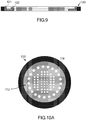
- the removable gas distribution plate 110 can comprise gas distribution nozzles 113 having a diameter of less than 8 mm, preferably less than 5.5 mm, more preferably less than 3 mm.
- the removable gas distribution plate 110 according to the invention can be composed of a porous plate, such as porous ceramic.
- the gas distribution module 100 is connected to gas cylinders positioned outside the reactor. A part of the gas distribution module 100 is preferably located above the resonant cavity 41 and close to the wave coupling module 80. By “located near”, it should be understood that the gas distribution module 100 comprises gas distribution nozzles 113 for injecting the gases into the resonant cavity 41 located less than 15 cm, preferably less than 10 cm, more preferably less than 5 cm from the dielectric window 82.
Landscapes
- Chemical & Material Sciences (AREA)
- Engineering & Computer Science (AREA)
- Physics & Mathematics (AREA)
- Plasma & Fusion (AREA)
- Analytical Chemistry (AREA)
- Materials Engineering (AREA)
- Metallurgy (AREA)
- Organic Chemistry (AREA)
- General Chemical & Material Sciences (AREA)
- Chemical Kinetics & Catalysis (AREA)
- Mechanical Engineering (AREA)
- Crystallography & Structural Chemistry (AREA)
- Inorganic Chemistry (AREA)
- Crystals, And After-Treatments Of Crystals (AREA)
- Chemical Vapour Deposition (AREA)
- Plasma Technology (AREA)
Claims (18)
- Modularer Reaktor für mikrowellenplasmaunterstützte Abscheidung (1) für die Herstellung von synthetischem Diamant, wobei der Reaktor umfasst:- einen Mikrowellengenerator (70), der zur Erzeugung von Mikrowellen mit einer Frequenz zwischen 300 MHz und 3000 MHz konfiguriert ist,- eine Resonanzkavität (41), die mindestens zum Teil von den zylindrischen Innenwänden (420) eines Behälters des Reaktors (400) gebildet ist,- ein Gaseinlasssystem (10), das imstande ist, Gase in die Resonanzkavität (41) zu befördern,- ein Gasauslassmodul (60), das imstande ist, die Gase aus der Resonanzkavität (41) abzuleiten,- ein Wellenkopplungsmodul (80), das imstande ist, die Mikrowellen vom Mikrowellengenerator (70) zur Resonanzkavität (41) weiterzuleiten, so dass die Bildung eines Plasmas gestattet wird, und- eine Wachstumsunterlage (51), die in der Resonanzkavität (41) vorhanden ist,wobei der modulare Reaktor mindestens drei Modulationselemente umfasst, wobei die Modulationselemente ausgewählt sind aus:- einem Kranz (450), der imstande ist, zwischen einem ersten Behälterabschnitt (430) und einem zweiten Behälterabschnitt (440) derart positioniert zu sein, dass die Form und/oder das Volumen der Resonanzkavität (41) verändert werden, und ein Dichtungssystem (460), welches die Dichtigkeit im Hinblick auf das Vakuum und die elektrische Kontinuität der Wände des Behälters erlaubt, zwischen dem Kranz (450) und jeweils dem ersten Behälterabschnitt (430) und dem zweiten Abschnitt (440) des Behälters (400) angeordnet ist;- einem Substratträgermodul (500) und einer Viertelwelle (501), wobei das Substratträgermodul, das vertikal translatorisch und rotatorisch beweglich ist, mit der Viertelwelle (501) im Kontakt ist und mindestens ein Fluidkühlsystem (520) aufweist;- einer Platte (900), die derart vertikal translatorisch beweglich ist, dass die Form und das Volumen der Resonanzkavität (41) verändert werden und Durchgangsöffnungen (911) aufweist, die den Durchgang der Gase erlauben;- einem Gasverteilungsmodul (100), aufweisend:∘ eine lösbare Gasverteilerplatte (110), umfassend eine innere Fläche (111), eine äußere Fläche (112) und eine Vielzahl von Gasverteilerdüsen (113), die Kanäle zwischen den Flächen (111, 112) bilden, die imstande sind, einen Gasstrom zu führen, und∘ eine Stützvorrichtung (120), die mit einem Kühlsystem verbunden ist und imstande, die lösbare Gasverteilerplatte (110) aufzunehmen; und- einem Steuermodul der Kühlung des Substrats (300), aufweisend eine lösbare Einleitungsvorrichtung thermisch resistenter Gase (330), wobei die lösbare Einleitungsvorrichtung thermisch resistenter Gase (330) einen oder mehrere Einlässe thermisch resistenter Gase (333) und einen oder mehrere Auslässe thermisch resistenter Gase (331) aufweist.
- Reaktor nach Anspruch 1, dadurch gekennzeichnet, dass er mindestens vier Modulationselemente umfasst, wobei die Modulationselemente ausgewählt sind aus:- einem Kranz (450), der imstande ist, zwischen einem ersten Behälterabschnitt (430) und einem zweiten Behälterabschnitt (440) derart positioniert zu sein, dass die Form und/oder das Volumen der Resonanzkavität (41) verändert werden, und ein Dichtungssystem (460), welches die Dichtigkeit im Hinblick auf das Vakuum und die elektrische Kontinuität der Wände des Behälters erlaubt, zwischen dem Kranz (450) und jeweils dem ersten Behälterabschnitt (430) und dem zweiten Abschnitt (440) des Behälters (400) angeordnet ist;- einem Substratträgermodul (500) und einer Viertelwelle (501), wobei das Substratträgermodul, das vertikal translatorisch und rotatorisch beweglich ist, mit der Viertelwelle (501) im Kontakt ist und mindestens ein Fluidkühlsystem (520) aufweist;- einer Platte (900), die derart vertikal translatorisch beweglich ist, dass die Form und das Volumen der Resonanzkavität (41) verändert werden und Durchgangsöffnungen (911) aufweist, die den Durchgang der Gase erlauben;- einem Gasverteilungsmodul (100), aufweisend:∘ eine lösbare Gasverteilerplatte (110), umfassend eine innere Fläche (111), eine äußere Fläche (112) und eine Vielzahl von Gasverteilerdüsen (113), die Kanäle zwischen den Flächen (111, 112) bilden, die imstande sind, einen Gasstrom zu führen, und∘ eine Stützvorrichtung (120), die mit einem Kühlsystem verbunden ist und imstande, die lösbare Gasverteilerplatte (110) aufzunehmen; und- einem Steuermodul der Kühlung des Substrats (300), aufweisend eine lösbare Einleitungsvorrichtung thermisch resistenter Gase (330), wobei die lösbare Einleitungsvorrichtung thermisch resistenter Gase (330) einen oder mehrere Einlässe thermisch resistenter Gase (333) und einen oder mehrere Auslässe thermisch resistenter Gase (331) aufweist.
- Reaktor nach einem der Ansprüche 1 oder 2, dadurch gekennzeichnet, dass er mindestens einen Kranz (450) umfasst, der imstande ist, zwischen einem ersten Behälterabschnitt (430) und einem zweiten Behälterabschnitt (440) derart positioniert zu sein, dass die Form und/oder das Volumen der Resonanzkavität (41) verändert werden, und ein Dichtungssystem (460), welches die Dichtigkeit im Hinblick auf das Vakuum und die elektrische Kontinuität der Wände des Behälters erlaubt, zwischen dem Kranz (450) und jeweils dem ersten Behälterabschnitt (430) und dem zweiten Abschnitt (440) des Behälters (400) angeordnet ist.
- Reaktor nach einem der Ansprüche 1 bis 3, dadurch gekennzeichnet, dass er zwei Kränze (450) umfasst.
- Reaktor nach einem der Ansprüche 1 bis 4, dadurch gekennzeichnet, dass der oder die Kränze (450) eine Höhe aufweisen, die zwischen 1 cm und 20 cm liegt.
- Reaktor nach einem der Ansprüche 1 bis 5, dadurch gekennzeichnet, dass der oder die Kränze (450) ein dielektrisches Material, ein Gaseinleitungssystem aufweisen oder aus Metall mit einem Innendurchmesser bestehen, der kleiner als der Innendurchmesser der Resonanzkavität (41) ist.
- Reaktor nach einem der Ansprüche 1 bis 6, dadurch gekennzeichnet, dass er ein Substratträgermodul (500) und eine Viertelwelle (501) umfasst, wobei das Substratträgermodul, das vertikal translatorisch und rotatorisch beweglich ist, mit der Viertelwelle (501) im Kontakt ist und mindestens ein Fluidkühlsystem (520) aufweist.
- Reaktor nach einem der Ansprüche 1 bis 7, dadurch gekennzeichnet, dass das Substratträgermodul (500) vom Behälter (400) und/oder von der Platte (900) elektrisch isoliert ist.
- Reaktor nach einem der Ansprüche 1 bis 8, dadurch gekennzeichnet, dass er eine Platte (900) umfasst, die derart vertikal translatorisch beweglich ist, dass die Form und das Volumen der Resonanzkavität (41) verändert werden und Durchgangsöffnungen (911) aufweist, die den Durchgang der Gase erlauben.
- Reaktor nach einem der Ansprüche 1 bis 9, dadurch gekennzeichnet, dass die Platte (900) mindestens einen Kühlkanal (930) aufweist, der mit einem Kühlsystem (940) verbunden ist und imstande, die Platte (900) zu kühlen.
- Reaktor nach einem der Ansprüche 1 bis 10, dadurch gekennzeichnet, dass er ein Gasverteilungsmodul (100) umfasst, aufweisend:- eine lösbare Gasverteilerplatte (110), umfassend eine innere Fläche (111), eine äußere Fläche (112) und eine Vielzahl von Gasverteilerdüsen (113), die Kanäle zwischen den Flächen (111, 112) bilden, die imstande sind, einen Gasstrom zu führen, und- eine Stützvorrichtung (120), die mit einem Kühlsystem verbunden ist und imstande, die lösbare Gasverteilerplatte (110) aufzunehmen.
- Reaktor nach einem der Ansprüche 1 bis 11, dadurch gekennzeichnet, dass die Stützvorrichtung (120) Kanäle (121) umfasst, die imstande sind, ein Gas oder eine Flüssigkeit in der Stützvorrichtung (120) zirkulieren zu lassen.
- Reaktor nach einem der Ansprüche 1 bis 12, dadurch gekennzeichnet, dass die lösbare Gasverteilerplatte (110) mindestens einen Endabschnitt (116) aufweist, der keine Verteilerdüsen (113) umfasst und imstande ist, mit der Stützvorrichtung (120) auf einer Fläche im Kontakt zu sein, die größer als oder gleich 10 % der Fläche der lösbaren Gasverteilerplatte (110) ist, so dass der thermische Transfer verbessert wird.
- Reaktor nach einem der Ansprüche 1 bis 13, dadurch gekennzeichnet, dass er ein Steuermodul der Kühlung des Substrats (300) umfasst, aufweisend eine lösbare Einleitungsvorrichtung thermisch resistenter Gase (330), wobei die lösbare Einleitungsvorrichtung thermisch resistenter Gase (330) einen oder mehrere Einlässe thermisch resistenter Gase (333) und einen oder mehrere Auslässe thermisch resistenter Gase (331) aufweist.
- Reaktor nach einem der Ansprüche 1 bis 14, dadurch gekennzeichnet, dass das Steuermodul der Kühlung des Substrats (300) Positionierungsmittel (320) umfasst und dass die Wachstumsunterlage (51) auf ihrer unteren Fläche Aussparungen aufweist, die imstande sind, die Positionierungsmittel (320) aufzunehmen.
- Reaktor nach einem der Ansprüche 1 bis 15, dadurch gekennzeichnet, dass das Steuermodul der Kühlung des Substrats (300) vertikal translatorisch bewegliche Positionierungsmittel (320) umfasst.
- Reaktor nach einem der Ansprüche 1 bis 16, dadurch gekennzeichnet, dass sich das Wellenkopplungsmodul (80) im oberen Abschnitt des ersten Abschnitts des Behälters (430) und mindestens 25 cm von unten des zweiten Behälterabschnitts (440) befindet.
- Verfahren zur Diamantsynthese, bei dem ein Reaktor für mikrowellenplasmaunterstützte Abscheidung für die Herstellung von synthetischem Diamant zum Einsatz kommt, wobei das Verfahren die folgenden Schritte umfasst:- Platzieren (810) des oder der Substrate auf die Wachstumsunterlage (51) des modularen Reaktors (1) nach einem der vorangehenden Ansprüche,- Inbetriebsetzen (820) des modularen Reaktors (1), wobei das Inbetriebsetzen die folgenden Schritte umfasst:∘ Erzeugen eines Drucks, der zwischen 0,2 hPa und 500 hPa liegt, innerhalb der Resonanzkavität (41), die im Transmissionsmodus TM011 arbeitet,∘ Einleiten der Mikrowellen mit einer Leistung, die beispielsweise bei einer Leistung zwischen 1 kW und 100 kW liegt,∘ Einleiten der Gase, beispielsweise in einer Gesamtmenge von mindestens 500 cm3 je Minute, und∘ Inbetriebnehmen der Kühlsysteme des Behälters, des Gaseinleitungssystems und des Substratträgers sowie eines Steuerungssystems der Kühlung des Substrats, um die Temperatur der Wachstumsfläche(n) zu steuern, und- Durchführen eines Wachstums (840) des Diamantfilms.
Applications Claiming Priority (2)
| Application Number | Priority Date | Filing Date | Title |
|---|---|---|---|
| FR1670746A FR3060024B1 (fr) | 2016-12-09 | 2016-12-09 | Reacteur modulaire pour le depot assiste par plasma microonde |
| PCT/FR2017/053482 WO2018104689A1 (fr) | 2016-12-09 | 2017-12-08 | Réacteur modulaire pour le dépôt assisté par plasma microonde |
Publications (2)
| Publication Number | Publication Date |
|---|---|
| EP3541971A1 EP3541971A1 (de) | 2019-09-25 |
| EP3541971B1 true EP3541971B1 (de) | 2020-04-01 |
Family
ID=58010109
Family Applications (1)
| Application Number | Title | Priority Date | Filing Date |
|---|---|---|---|
| EP17822395.4A Active EP3541971B1 (de) | 2016-12-09 | 2017-12-08 | Modularer reaktor für mikrowellenplasmaunterstützte abscheidung und entsprechendes diamantsyntheseverfahren |
Country Status (9)
| Country | Link |
|---|---|
| US (1) | US11859279B2 (de) |
| EP (1) | EP3541971B1 (de) |
| JP (1) | JP7045090B2 (de) |
| CN (1) | CN110268095B (de) |
| CA (1) | CA3046528A1 (de) |
| ES (1) | ES2801850T3 (de) |
| FR (1) | FR3060024B1 (de) |
| RU (1) | RU2725428C1 (de) |
| WO (1) | WO2018104689A1 (de) |
Families Citing this family (10)
| Publication number | Priority date | Publication date | Assignee | Title |
|---|---|---|---|---|
| US11469077B2 (en) * | 2018-04-24 | 2022-10-11 | FD3M, Inc. | Microwave plasma chemical vapor deposition device and application thereof |
| US20200263285A1 (en) | 2018-08-02 | 2020-08-20 | Lyten, Inc. | Covetic materials |
| CN110468449B (zh) * | 2019-09-12 | 2021-09-07 | 宁波晨鑫维克工业科技有限公司 | 用于制造单晶金刚石的微波等离子体反应器及其扩散装置 |
| CN113106418B (zh) * | 2020-12-17 | 2025-02-07 | 芯三代半导体科技(苏州)股份有限公司 | 抽气装置 |
| CN113417007A (zh) * | 2021-06-23 | 2021-09-21 | 秦皇岛本征晶体科技有限公司 | 一种基于气流系统结构控制金刚石沉积速率的方法 |
| US20220415668A1 (en) * | 2021-06-24 | 2022-12-29 | Taiwan Semiconductor Manufacturing Co., Lid. | Annealing system and method for using the same |
| CN115110148B (zh) * | 2022-07-01 | 2023-12-05 | 安徽光智科技有限公司 | 一种单晶金刚石的制备方法 |
| CN115537781B (zh) * | 2022-10-27 | 2024-10-22 | 上海埃延半导体有限公司 | 一种弥漫层流反应腔体及控制方法 |
| US20240240354A1 (en) * | 2023-01-17 | 2024-07-18 | Plasmability, Llc | Method of Growing Personalized Single Crystal Diamond |
| US20250210315A1 (en) * | 2023-12-21 | 2025-06-26 | Applied Materials, Inc. | Modular processing chambers and related heating configurations, methods, apparatus, and modules for semiconductor manufacturing |
Family Cites Families (23)
| Publication number | Priority date | Publication date | Assignee | Title |
|---|---|---|---|---|
| JPH01179323A (ja) * | 1988-01-06 | 1989-07-17 | Hitachi Ltd | プラズマ反応装置 |
| JPH10134997A (ja) * | 1996-10-24 | 1998-05-22 | Samsung Electron Co Ltd | 2次電位による放電を除去したプラズマ処理装置 |
| US20040194890A1 (en) | 2001-09-28 | 2004-10-07 | Tokyo Electron Limited | Hybrid plasma processing apparatus |
| US7311784B2 (en) | 2002-11-26 | 2007-12-25 | Tokyo Electron Limited | Plasma processing device |
| TW200537695A (en) * | 2004-03-19 | 2005-11-16 | Adv Lcd Tech Dev Ct Co Ltd | Insulating film forming method, insulating film forming apparatus, and plasma film forming apparatus |
| JP4624856B2 (ja) * | 2005-05-30 | 2011-02-02 | 東京エレクトロン株式会社 | プラズマ処理装置 |
| JP2008262968A (ja) | 2007-04-10 | 2008-10-30 | Tokyo Electron Ltd | プラズマ処理装置およびプラズマ処理方法 |
| WO2009114130A2 (en) | 2008-03-13 | 2009-09-17 | Michigan State University | Process and apparatus for diamond synthesis |
| US9890457B2 (en) | 2008-06-16 | 2018-02-13 | Board Of Trustees Of Michigan State University | Microwave plasma reactors |
| SG191220A1 (en) * | 2010-12-23 | 2013-07-31 | Element Six Ltd | Controlling doping of synthetic diamond material |
| GB201021855D0 (en) | 2010-12-23 | 2011-02-02 | Element Six Ltd | Microwave power delivery system for plasma reactors |
| GB201021853D0 (en) * | 2010-12-23 | 2011-02-02 | Element Six Ltd | A microwave plasma reactor for manufacturing synthetic diamond material |
| GB201021865D0 (en) * | 2010-12-23 | 2011-02-02 | Element Six Ltd | A microwave plasma reactor for manufacturing synthetic diamond material |
| GB201021870D0 (en) | 2010-12-23 | 2011-02-02 | Element Six Ltd | A microwave plasma reactor for manufacturing synthetic diamond material |
| GB201021913D0 (en) * | 2010-12-23 | 2011-02-02 | Element Six Ltd | Microwave plasma reactors and substrates for synthetic diamond manufacture |
| GB201121640D0 (en) * | 2011-12-16 | 2012-01-25 | Element Six Ltd | Large area optical synthetic polycrystalline diamond window |
| US9720133B2 (en) * | 2011-12-16 | 2017-08-01 | Element Six Technologies Limited | Large area optical quality synthetic polycrystalline diamond window |
| GB2523881B (en) | 2011-12-16 | 2016-06-15 | Element Six Tech Ltd | Large area optical quality synthetic polycrystalline diamond window |
| US20140051253A1 (en) | 2012-08-14 | 2014-02-20 | Lam Research Corporation | Plasma baffle ring for a plasma processing apparatus and method of use |
| GB201320304D0 (en) * | 2013-11-18 | 2014-01-01 | Element Six Ltd | Methods of fabricating synthetic diamond materials using microwave plasma actived chemical vapour deposition techniques and products obtained using said |
| US9435031B2 (en) | 2014-01-07 | 2016-09-06 | International Business Machines Corporation | Microwave plasma and ultraviolet assisted deposition apparatus and method for material deposition using the same |
| FR3022563B1 (fr) | 2014-06-23 | 2016-07-15 | Univ Paris Xiii Paris-Nord Villetaneuse | Procede de formation d'un monocristal de materiau a partir d'un substrat monocristallin |
| KR102417178B1 (ko) * | 2015-09-03 | 2022-07-05 | 삼성전자주식회사 | 마이크로파 탐침, 그 탐침을 구비한 플라즈마 모니터링 시스템, 및 그 시스템을 이용한 반도체 소자 제조방법 |
-
2016
- 2016-12-09 FR FR1670746A patent/FR3060024B1/fr active Active
-
2017
- 2017-12-08 ES ES17822395T patent/ES2801850T3/es active Active
- 2017-12-08 JP JP2019551757A patent/JP7045090B2/ja active Active
- 2017-12-08 EP EP17822395.4A patent/EP3541971B1/de active Active
- 2017-12-08 RU RU2019120472A patent/RU2725428C1/ru active
- 2017-12-08 US US16/467,828 patent/US11859279B2/en active Active
- 2017-12-08 CN CN201780086193.9A patent/CN110268095B/zh active Active
- 2017-12-08 WO PCT/FR2017/053482 patent/WO2018104689A1/fr not_active Ceased
- 2017-12-08 CA CA3046528A patent/CA3046528A1/fr active Pending
Also Published As
| Publication number | Publication date |
|---|---|
| CN110268095A (zh) | 2019-09-20 |
| WO2018104689A1 (fr) | 2018-06-14 |
| JP2020520869A (ja) | 2020-07-16 |
| FR3060024B1 (fr) | 2019-05-31 |
| CN110268095B (zh) | 2021-12-28 |
| ES2801850T3 (es) | 2021-01-14 |
| FR3060024A1 (fr) | 2018-06-15 |
| US11859279B2 (en) | 2024-01-02 |
| JP7045090B2 (ja) | 2022-03-31 |
| RU2725428C1 (ru) | 2020-07-02 |
| US20210087676A1 (en) | 2021-03-25 |
| EP3541971A1 (de) | 2019-09-25 |
| CA3046528A1 (fr) | 2018-06-14 |
Similar Documents
| Publication | Publication Date | Title |
|---|---|---|
| EP3541971B1 (de) | Modularer reaktor für mikrowellenplasmaunterstützte abscheidung und entsprechendes diamantsyntheseverfahren | |
| Nad et al. | Growth strategies for large and high quality single crystal diamond substrates | |
| EP2255029B1 (de) | Verfahren zur herstellung von nanostrukturen auf metalloxidsubstrat und dünnfilmvorrichtung | |
| EP0231544B1 (de) | Reaktionskammer für Epitaxiekristallzüchtung aus gasförmiger Phase von Halbleitermaterialien | |
| JP2015504972A (ja) | 大面積高光学的特性型合成多結晶ダイヤモンド窓 | |
| EP0263788B1 (de) | Verfahren und Vorrichtung zum Auftragen von hydriertem, amorphem Silizium auf ein Substrat in Plasmaumgebung | |
| EP4587625A1 (de) | Verfahren zur herstellung einer monokristallinen diamantplatte, monokristalline diamantplatte und einkristalline diamantscheibe grosser grösse | |
| EP2110458B1 (de) | Wärmebehandlungsofen mit Induktionsheizung | |
| EP2978871B1 (de) | Verfahren für eine diamantdampfabscheidung | |
| EP3325696B1 (de) | Beseitigung von versetzungen bei einem einkristall | |
| EP3568505B1 (de) | Behandlungskammer für einen reaktor zur chemischen gasphasenabscheidung (cvd) und in dieser kammer ausgeführter thermalisierungsprozess | |
| EP0522986A1 (de) | Verfahren und Vorrichtung zur Diamantabscheidung mittels Mikrowellen-Plasma CVD | |
| FR2664389A1 (fr) | Articles optiques resistant au rayonnement faits d'un diamant monocristallin a haute purete isotopique. | |
| FR2995913A1 (fr) | Procede de formation d'une couche de silicium epitaxiee. | |
| FR3148444A1 (fr) | Procede de synthese de diamant par plasmas micro-ondes distribues | |
| WO2024089359A1 (fr) | Procédé de formation d'une couche de carbure de silicium | |
| FR2646861A1 (fr) | Appareil de traitement de substrats plans sous vide partiel | |
| EP3129518A1 (de) | Verfahren zur herstellung einer graphenfolie | |
| WO2016024877A1 (ru) | Способ получения легированных халькогенидов цинка | |
| HK40012284B (en) | Modular reactor for microwave plasma-assisted deposition and corresponding diamond synthesis method | |
| HK40012284A (en) | Modular reactor for microwave plasma-assisted deposition and corresponding diamond synthesis method | |
| CH707800B1 (fr) | Procédé de dépôt de diamant en phase vapeur et équipement pour réaliser ce procédé. | |
| FR2606038A1 (fr) | Perfectionnement aux enceintes pour le traitement des substrats semiconducteurs |
Legal Events
| Date | Code | Title | Description |
|---|---|---|---|
| STAA | Information on the status of an ep patent application or granted ep patent |
Free format text: STATUS: UNKNOWN |
|
| STAA | Information on the status of an ep patent application or granted ep patent |
Free format text: STATUS: THE INTERNATIONAL PUBLICATION HAS BEEN MADE |
|
| PUAI | Public reference made under article 153(3) epc to a published international application that has entered the european phase |
Free format text: ORIGINAL CODE: 0009012 |
|
| STAA | Information on the status of an ep patent application or granted ep patent |
Free format text: STATUS: REQUEST FOR EXAMINATION WAS MADE |
|
| GRAP | Despatch of communication of intention to grant a patent |
Free format text: ORIGINAL CODE: EPIDOSNIGR1 |
|
| STAA | Information on the status of an ep patent application or granted ep patent |
Free format text: STATUS: GRANT OF PATENT IS INTENDED |
|
| 17P | Request for examination filed |
Effective date: 20190621 |
|
| AK | Designated contracting states |
Kind code of ref document: A1 Designated state(s): AL AT BE BG CH CY CZ DE DK EE ES FI FR GB GR HR HU IE IS IT LI LT LU LV MC MK MT NL NO PL PT RO RS SE SI SK SM TR |
|
| AX | Request for extension of the european patent |
Extension state: BA ME |
|
| INTG | Intention to grant announced |
Effective date: 20190924 |
|
| GRAS | Grant fee paid |
Free format text: ORIGINAL CODE: EPIDOSNIGR3 |
|
| GRAA | (expected) grant |
Free format text: ORIGINAL CODE: 0009210 |
|
| STAA | Information on the status of an ep patent application or granted ep patent |
Free format text: STATUS: THE PATENT HAS BEEN GRANTED |
|
| DAV | Request for validation of the european patent (deleted) | ||
| DAX | Request for extension of the european patent (deleted) | ||
| AK | Designated contracting states |
Kind code of ref document: B1 Designated state(s): AL AT BE BG CH CY CZ DE DK EE ES FI FR GB GR HR HU IE IS IT LI LT LU LV MC MK MT NL NO PL PT RO RS SE SI SK SM TR |
|
| REG | Reference to a national code |
Ref country code: GB Ref legal event code: FG4D Free format text: NOT ENGLISH |
|
| REG | Reference to a national code |
Ref country code: CH Ref legal event code: EP Ref country code: AT Ref legal event code: REF Ref document number: 1251423 Country of ref document: AT Kind code of ref document: T Effective date: 20200415 |
|
| REG | Reference to a national code |
Ref country code: DE Ref legal event code: R096 Ref document number: 602017014146 Country of ref document: DE |
|
| REG | Reference to a national code |
Ref country code: IE Ref legal event code: FG4D Free format text: LANGUAGE OF EP DOCUMENT: FRENCH |
|
| REG | Reference to a national code |
Ref country code: CH Ref legal event code: NV Representative=s name: DENNEMEYER AG, CH |
|
| REG | Reference to a national code |
Ref country code: HK Ref legal event code: DE Ref document number: 40012284 Country of ref document: HK |
|
| REG | Reference to a national code |
Ref country code: NL Ref legal event code: FP |
|
| PG25 | Lapsed in a contracting state [announced via postgrant information from national office to epo] |
Ref country code: BG Free format text: LAPSE BECAUSE OF FAILURE TO SUBMIT A TRANSLATION OF THE DESCRIPTION OR TO PAY THE FEE WITHIN THE PRESCRIBED TIME-LIMIT Effective date: 20200701 |
|
| REG | Reference to a national code |
Ref country code: LT Ref legal event code: MG4D |
|
| PG25 | Lapsed in a contracting state [announced via postgrant information from national office to epo] |
Ref country code: SE Free format text: LAPSE BECAUSE OF FAILURE TO SUBMIT A TRANSLATION OF THE DESCRIPTION OR TO PAY THE FEE WITHIN THE PRESCRIBED TIME-LIMIT Effective date: 20200401 Ref country code: LT Free format text: LAPSE BECAUSE OF FAILURE TO SUBMIT A TRANSLATION OF THE DESCRIPTION OR TO PAY THE FEE WITHIN THE PRESCRIBED TIME-LIMIT Effective date: 20200401 Ref country code: CZ Free format text: LAPSE BECAUSE OF FAILURE TO SUBMIT A TRANSLATION OF THE DESCRIPTION OR TO PAY THE FEE WITHIN THE PRESCRIBED TIME-LIMIT Effective date: 20200401 Ref country code: FI Free format text: LAPSE BECAUSE OF FAILURE TO SUBMIT A TRANSLATION OF THE DESCRIPTION OR TO PAY THE FEE WITHIN THE PRESCRIBED TIME-LIMIT Effective date: 20200401 Ref country code: GR Free format text: LAPSE BECAUSE OF FAILURE TO SUBMIT A TRANSLATION OF THE DESCRIPTION OR TO PAY THE FEE WITHIN THE PRESCRIBED TIME-LIMIT Effective date: 20200702 Ref country code: PT Free format text: LAPSE BECAUSE OF FAILURE TO SUBMIT A TRANSLATION OF THE DESCRIPTION OR TO PAY THE FEE WITHIN THE PRESCRIBED TIME-LIMIT Effective date: 20200817 Ref country code: IS Free format text: LAPSE BECAUSE OF FAILURE TO SUBMIT A TRANSLATION OF THE DESCRIPTION OR TO PAY THE FEE WITHIN THE PRESCRIBED TIME-LIMIT Effective date: 20200801 Ref country code: NO Free format text: LAPSE BECAUSE OF FAILURE TO SUBMIT A TRANSLATION OF THE DESCRIPTION OR TO PAY THE FEE WITHIN THE PRESCRIBED TIME-LIMIT Effective date: 20200701 |
|
| REG | Reference to a national code |
Ref country code: AT Ref legal event code: MK05 Ref document number: 1251423 Country of ref document: AT Kind code of ref document: T Effective date: 20200401 |
|
| PG25 | Lapsed in a contracting state [announced via postgrant information from national office to epo] |
Ref country code: LV Free format text: LAPSE BECAUSE OF FAILURE TO SUBMIT A TRANSLATION OF THE DESCRIPTION OR TO PAY THE FEE WITHIN THE PRESCRIBED TIME-LIMIT Effective date: 20200401 Ref country code: HR Free format text: LAPSE BECAUSE OF FAILURE TO SUBMIT A TRANSLATION OF THE DESCRIPTION OR TO PAY THE FEE WITHIN THE PRESCRIBED TIME-LIMIT Effective date: 20200401 Ref country code: RS Free format text: LAPSE BECAUSE OF FAILURE TO SUBMIT A TRANSLATION OF THE DESCRIPTION OR TO PAY THE FEE WITHIN THE PRESCRIBED TIME-LIMIT Effective date: 20200401 |
|
| PG25 | Lapsed in a contracting state [announced via postgrant information from national office to epo] |
Ref country code: AL Free format text: LAPSE BECAUSE OF FAILURE TO SUBMIT A TRANSLATION OF THE DESCRIPTION OR TO PAY THE FEE WITHIN THE PRESCRIBED TIME-LIMIT Effective date: 20200401 |
|
| REG | Reference to a national code |
Ref country code: DE Ref legal event code: R097 Ref document number: 602017014146 Country of ref document: DE |
|
| REG | Reference to a national code |
Ref country code: ES Ref legal event code: FG2A Ref document number: 2801850 Country of ref document: ES Kind code of ref document: T3 Effective date: 20210114 |
|
| PG25 | Lapsed in a contracting state [announced via postgrant information from national office to epo] |
Ref country code: RO Free format text: LAPSE BECAUSE OF FAILURE TO SUBMIT A TRANSLATION OF THE DESCRIPTION OR TO PAY THE FEE WITHIN THE PRESCRIBED TIME-LIMIT Effective date: 20200401 Ref country code: DK Free format text: LAPSE BECAUSE OF FAILURE TO SUBMIT A TRANSLATION OF THE DESCRIPTION OR TO PAY THE FEE WITHIN THE PRESCRIBED TIME-LIMIT Effective date: 20200401 Ref country code: SM Free format text: LAPSE BECAUSE OF FAILURE TO SUBMIT A TRANSLATION OF THE DESCRIPTION OR TO PAY THE FEE WITHIN THE PRESCRIBED TIME-LIMIT Effective date: 20200401 Ref country code: EE Free format text: LAPSE BECAUSE OF FAILURE TO SUBMIT A TRANSLATION OF THE DESCRIPTION OR TO PAY THE FEE WITHIN THE PRESCRIBED TIME-LIMIT Effective date: 20200401 Ref country code: AT Free format text: LAPSE BECAUSE OF FAILURE TO SUBMIT A TRANSLATION OF THE DESCRIPTION OR TO PAY THE FEE WITHIN THE PRESCRIBED TIME-LIMIT Effective date: 20200401 |
|
| PLBE | No opposition filed within time limit |
Free format text: ORIGINAL CODE: 0009261 |
|
| STAA | Information on the status of an ep patent application or granted ep patent |
Free format text: STATUS: NO OPPOSITION FILED WITHIN TIME LIMIT |
|
| PG25 | Lapsed in a contracting state [announced via postgrant information from national office to epo] |
Ref country code: PL Free format text: LAPSE BECAUSE OF FAILURE TO SUBMIT A TRANSLATION OF THE DESCRIPTION OR TO PAY THE FEE WITHIN THE PRESCRIBED TIME-LIMIT Effective date: 20200401 Ref country code: SK Free format text: LAPSE BECAUSE OF FAILURE TO SUBMIT A TRANSLATION OF THE DESCRIPTION OR TO PAY THE FEE WITHIN THE PRESCRIBED TIME-LIMIT Effective date: 20200401 |
|
| 26N | No opposition filed |
Effective date: 20210112 |
|
| PG25 | Lapsed in a contracting state [announced via postgrant information from national office to epo] |
Ref country code: MC Free format text: LAPSE BECAUSE OF FAILURE TO SUBMIT A TRANSLATION OF THE DESCRIPTION OR TO PAY THE FEE WITHIN THE PRESCRIBED TIME-LIMIT Effective date: 20200401 |
|
| PG25 | Lapsed in a contracting state [announced via postgrant information from national office to epo] |
Ref country code: LU Free format text: LAPSE BECAUSE OF NON-PAYMENT OF DUE FEES Effective date: 20201208 |
|
| PG25 | Lapsed in a contracting state [announced via postgrant information from national office to epo] |
Ref country code: TR Free format text: LAPSE BECAUSE OF FAILURE TO SUBMIT A TRANSLATION OF THE DESCRIPTION OR TO PAY THE FEE WITHIN THE PRESCRIBED TIME-LIMIT Effective date: 20200401 Ref country code: MT Free format text: LAPSE BECAUSE OF FAILURE TO SUBMIT A TRANSLATION OF THE DESCRIPTION OR TO PAY THE FEE WITHIN THE PRESCRIBED TIME-LIMIT Effective date: 20200401 Ref country code: CY Free format text: LAPSE BECAUSE OF FAILURE TO SUBMIT A TRANSLATION OF THE DESCRIPTION OR TO PAY THE FEE WITHIN THE PRESCRIBED TIME-LIMIT Effective date: 20200401 |
|
| PG25 | Lapsed in a contracting state [announced via postgrant information from national office to epo] |
Ref country code: MK Free format text: LAPSE BECAUSE OF FAILURE TO SUBMIT A TRANSLATION OF THE DESCRIPTION OR TO PAY THE FEE WITHIN THE PRESCRIBED TIME-LIMIT Effective date: 20200401 |
|
| PG25 | Lapsed in a contracting state [announced via postgrant information from national office to epo] |
Ref country code: SI Free format text: LAPSE BECAUSE OF FAILURE TO SUBMIT A TRANSLATION OF THE DESCRIPTION OR TO PAY THE FEE WITHIN THE PRESCRIBED TIME-LIMIT Effective date: 20200401 |
|
| PGFP | Annual fee paid to national office [announced via postgrant information from national office to epo] |
Ref country code: CH Payment date: 20250101 Year of fee payment: 8 |
|
| PGFP | Annual fee paid to national office [announced via postgrant information from national office to epo] |
Ref country code: NL Payment date: 20251119 Year of fee payment: 9 |
|
| REG | Reference to a national code |
Ref country code: CH Ref legal event code: U11 Free format text: ST27 STATUS EVENT CODE: U-0-0-U10-U11 (AS PROVIDED BY THE NATIONAL OFFICE) Effective date: 20260101 |
|
| PGFP | Annual fee paid to national office [announced via postgrant information from national office to epo] |
Ref country code: DE Payment date: 20251126 Year of fee payment: 9 |
|
| PGFP | Annual fee paid to national office [announced via postgrant information from national office to epo] |
Ref country code: GB Payment date: 20251119 Year of fee payment: 9 |
|
| PGFP | Annual fee paid to national office [announced via postgrant information from national office to epo] |
Ref country code: IT Payment date: 20251119 Year of fee payment: 9 |
|
| PGFP | Annual fee paid to national office [announced via postgrant information from national office to epo] |
Ref country code: FR Payment date: 20251231 Year of fee payment: 9 |
|
| PGFP | Annual fee paid to national office [announced via postgrant information from national office to epo] |
Ref country code: BE Payment date: 20251119 Year of fee payment: 9 |
|
| PGFP | Annual fee paid to national office [announced via postgrant information from national office to epo] |
Ref country code: IE Payment date: 20251121 Year of fee payment: 9 |
|
| PGFP | Annual fee paid to national office [announced via postgrant information from national office to epo] |
Ref country code: ES Payment date: 20260102 Year of fee payment: 9 |