EP3543733A1 - Photodétecteur, lidar et procédé de fabrication de photodétecteur - Google Patents
Photodétecteur, lidar et procédé de fabrication de photodétecteur Download PDFInfo
- Publication number
- EP3543733A1 EP3543733A1 EP18193685.7A EP18193685A EP3543733A1 EP 3543733 A1 EP3543733 A1 EP 3543733A1 EP 18193685 A EP18193685 A EP 18193685A EP 3543733 A1 EP3543733 A1 EP 3543733A1
- Authority
- EP
- European Patent Office
- Prior art keywords
- light detection
- photodetector
- semiconductor layer
- light
- detection element
- Prior art date
- Legal status (The legal status is an assumption and is not a legal conclusion. Google has not performed a legal analysis and makes no representation as to the accuracy of the status listed.)
- Withdrawn
Links
Images



Classifications
-
- G—PHYSICS
- G01—MEASURING; TESTING
- G01S—RADIO DIRECTION-FINDING; RADIO NAVIGATION; DETERMINING DISTANCE OR VELOCITY BY USE OF RADIO WAVES; LOCATING OR PRESENCE-DETECTING BY USE OF THE REFLECTION OR RERADIATION OF RADIO WAVES; ANALOGOUS ARRANGEMENTS USING OTHER WAVES
- G01S7/00—Details of systems according to groups G01S13/00, G01S15/00, G01S17/00
- G01S7/48—Details of systems according to groups G01S13/00, G01S15/00, G01S17/00 of systems according to group G01S17/00
- G01S7/483—Details of pulse systems
- G01S7/486—Receivers
- G01S7/4861—Circuits for detection, sampling, integration or read-out
- G01S7/4863—Detector arrays, e.g. charge-transfer gates
-
- G—PHYSICS
- G01—MEASURING; TESTING
- G01S—RADIO DIRECTION-FINDING; RADIO NAVIGATION; DETERMINING DISTANCE OR VELOCITY BY USE OF RADIO WAVES; LOCATING OR PRESENCE-DETECTING BY USE OF THE REFLECTION OR RERADIATION OF RADIO WAVES; ANALOGOUS ARRANGEMENTS USING OTHER WAVES
- G01S17/00—Systems using the reflection or reradiation of electromagnetic waves other than radio waves, e.g. lidar systems
- G01S17/02—Systems using the reflection of electromagnetic waves other than radio waves
- G01S17/06—Systems determining position data of a target
- G01S17/08—Systems determining position data of a target for measuring distance only
-
- G—PHYSICS
- G01—MEASURING; TESTING
- G01S—RADIO DIRECTION-FINDING; RADIO NAVIGATION; DETERMINING DISTANCE OR VELOCITY BY USE OF RADIO WAVES; LOCATING OR PRESENCE-DETECTING BY USE OF THE REFLECTION OR RERADIATION OF RADIO WAVES; ANALOGOUS ARRANGEMENTS USING OTHER WAVES
- G01S17/00—Systems using the reflection or reradiation of electromagnetic waves other than radio waves, e.g. lidar systems
- G01S17/02—Systems using the reflection of electromagnetic waves other than radio waves
- G01S17/06—Systems determining position data of a target
- G01S17/08—Systems determining position data of a target for measuring distance only
- G01S17/10—Systems determining position data of a target for measuring distance only using transmission of interrupted, pulse-modulated waves
-
- H—ELECTRICITY
- H10—SEMICONDUCTOR DEVICES; ELECTRIC SOLID-STATE DEVICES NOT OTHERWISE PROVIDED FOR
- H10F—INORGANIC SEMICONDUCTOR DEVICES SENSITIVE TO INFRARED RADIATION, LIGHT, ELECTROMAGNETIC RADIATION OF SHORTER WAVELENGTH OR CORPUSCULAR RADIATION
- H10F30/00—Individual radiation-sensitive semiconductor devices in which radiation controls the flow of current through the devices, e.g. photodetectors
- H10F30/20—Individual radiation-sensitive semiconductor devices in which radiation controls the flow of current through the devices, e.g. photodetectors the devices having potential barriers, e.g. phototransistors
- H10F30/21—Individual radiation-sensitive semiconductor devices in which radiation controls the flow of current through the devices, e.g. photodetectors the devices having potential barriers, e.g. phototransistors the devices being sensitive to infrared, visible or ultraviolet radiation
- H10F30/22—Individual radiation-sensitive semiconductor devices in which radiation controls the flow of current through the devices, e.g. photodetectors the devices having potential barriers, e.g. phototransistors the devices being sensitive to infrared, visible or ultraviolet radiation the devices having only one potential barrier, e.g. photodiodes
- H10F30/225—Individual radiation-sensitive semiconductor devices in which radiation controls the flow of current through the devices, e.g. photodetectors the devices having potential barriers, e.g. phototransistors the devices being sensitive to infrared, visible or ultraviolet radiation the devices having only one potential barrier, e.g. photodiodes the potential barrier working in avalanche mode, e.g. avalanche photodiodes
-
- H—ELECTRICITY
- H10—SEMICONDUCTOR DEVICES; ELECTRIC SOLID-STATE DEVICES NOT OTHERWISE PROVIDED FOR
- H10F—INORGANIC SEMICONDUCTOR DEVICES SENSITIVE TO INFRARED RADIATION, LIGHT, ELECTROMAGNETIC RADIATION OF SHORTER WAVELENGTH OR CORPUSCULAR RADIATION
- H10F39/00—Integrated devices, or assemblies of multiple devices, comprising at least one element covered by group H10F30/00, e.g. radiation detectors comprising photodiode arrays
- H10F39/10—Integrated devices
- H10F39/107—Integrated devices having multiple elements covered by H10F30/00 in a repetitive configuration, e.g. radiation detectors comprising photodiode arrays
-
- H—ELECTRICITY
- H10—SEMICONDUCTOR DEVICES; ELECTRIC SOLID-STATE DEVICES NOT OTHERWISE PROVIDED FOR
- H10F—INORGANIC SEMICONDUCTOR DEVICES SENSITIVE TO INFRARED RADIATION, LIGHT, ELECTROMAGNETIC RADIATION OF SHORTER WAVELENGTH OR CORPUSCULAR RADIATION
- H10F77/00—Constructional details of devices covered by this subclass
- H10F77/95—Circuit arrangements
- H10F77/953—Circuit arrangements for devices having potential barriers
- H10F77/959—Circuit arrangements for devices having potential barriers for devices working in avalanche mode
-
- G—PHYSICS
- G01—MEASURING; TESTING
- G01S—RADIO DIRECTION-FINDING; RADIO NAVIGATION; DETERMINING DISTANCE OR VELOCITY BY USE OF RADIO WAVES; LOCATING OR PRESENCE-DETECTING BY USE OF THE REFLECTION OR RERADIATION OF RADIO WAVES; ANALOGOUS ARRANGEMENTS USING OTHER WAVES
- G01S17/00—Systems using the reflection or reradiation of electromagnetic waves other than radio waves, e.g. lidar systems
- G01S17/88—Lidar systems specially adapted for specific applications
- G01S17/89—Lidar systems specially adapted for specific applications for mapping or imaging
- G01S17/894—Three-dimensional [3D] imaging with simultaneous measurement of time-of-flight at a two-dimensional [2D] array of receiver pixels, e.g. time-of-flight cameras or flash lidar
Definitions
- Embodiments relate to a photodetector, a Lidar and a method of manufacturing photodetector.
- a laser imaging detection and ranging (LIDAR) device is a distance image sensing system adopting a time-of-flight (TOF) distance measuring method of measuring a time when the laser light reciprocates to a target and converting the time into a distance, and the LIDAR device is applied to an in-vehicle drive-assist system, remote sensing, and the like.
- TOF time-of-flight
- a photodetector used in the LIDAR device includes one or more light detection elements.
- the light detection element is applied with a driving voltage for driving the light detection element to detect light.
- the driving voltage range is almost the same in all elements.
- Embodiments of the invention provide a photodetector having different driving voltage ranges and improved device characteristics.
- a photodetector includes a plurality of first light detection elements having a first driving voltage range, the first light detection elements including first semiconductor layers having a first conductivity type and second semiconductor layers having a second conductivity type different from the first conductivity type; and a second light detection element having a second driving voltage range different from the first driving voltage range, the second light detection element including a third semiconductor layer having the first conductivity type and a fourth semiconductor layer having the second conductivity type.
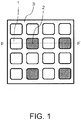
- Fig. 1 is a diagram illustrating a photodetector according to a first embodiment as viewed from a light incident side.
- This photodetector includes two types of light detection elements having different driving voltage ranges.
- the driving voltage range is a range of a voltage in which photoelectric conversion can be performed when light is incident on the light detection element.
- the photodetector includes a plurality of first light detection elements 1, at least one or more second light detection elements 2 provided between the first light detection elements 1, and a non-light detection region 3 provided between the first light detection elements 1 and between the first light detection element 1 and the second light detection element 2.
- the second light detection elements 2 are arranged not to be adjacent to each other, and thus, in this embodiment, the light detection elements are arranged so that the ratio of the number of the first light detection elements 1 and the number of the second light detection elements 2 is 3 : 1.
- the driving voltage range of the first light detection element 1 is set to be wider than the driving voltage range of the second light detection element 2.
- the first light detection element 1 and the second light detection element 2 detect light (for example, near infrared light) by converting the light into an electric signal.
- An avalanche photodiode (APD) may be exemplified.
- the first light detection element 1 and the second light detection element 2 have substantially the same opening area.
- the "substantially same” in this embodiment also includes an error of ⁇ 5%.
- the opening area is an area of the light detection element surrounded by the non-light detection region 3 as viewed from the light incident side.
- the near infrared light denotes light in a wavelength range of, for example, 780 nm or more and 2500 nm or less.
- the non-light detection region 3 is a region where incident light cannot be detected.
- the non-light detection region 3 is also a region where electrodes are present because the electric signals converted by the light detection elements 1 and 2 are respectively wired to a driving/reading unit to be described later.
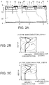
- Fig. 2A is a diagram illustrating a p-p' cross section of the photodetector illustrated in Fig. 1 .
- the photodetector includes a backside electrode 9, a high-concentration p-type substrate 11 provided on the backside electrode 9, and a p-type semiconductor layer 12 provided on the high-concentration p-type substrate 11.
- “on” is the side on which light is incident. The light incident side is the upper side in Fig. 2A .
- the first light detection elements 1 and the second light detection elements 2 are alternately provided on the upper surface of the p-type semiconductor layer 12, and an electrode 10 electrically connected to end portions of the upper surfaces of the first light detection element 1 and the second light detection element 2 and a protective layer 70 provided so as to cover the electrode 10 are provided.
- the electrode 10 is also arranged in the non-light detection region 3 in Fig. 1 .
- the first light detection element 1 includes a p + -type semiconductor layer 5 (corresponding to a first semiconductor layer) and an n + -type semiconductor layer 6 (corresponding to a second semiconductor layer) provided on the light incident side of the p + -type semiconductor layer 5, and the interface between the p + -type semiconductor layer 5 and the n + -type semiconductor layer 6 forms a pn junction.
- the width of the n + -type semiconductor layer 6 is larger than the width of the p + -type semiconductor layer 5.
- crossing denotes nearly perpendicular in this embodiment.
- the electrode 10 is electrically connected to an end portion of the upper surface of the n + -type semiconductor layer 6 of the first light detection element 1.
- the second light detection element 2 includes a p + -type semiconductor layer 7 (corresponding to a third semiconductor layer) and an n + -type semiconductor layer 8 (corresponding to a fourth semiconductor layer) provided on the light incident side of the p + -type semiconductor layer 7, and the interface between the p + -type semiconductor layer 7 and the n + -type semiconductor layer 8 forms a pn junction.
- the width of the n + -type semiconductor layer 8 is larger than the width of the p + -type semiconductor layer 7.
- the electrode 10 is electrically connected to an end portion of the upper surface of the n + -type semiconductor layer 8 of the second light detection element 2.
- the difference between the first light detection element 1 and the second light detection element 2 is that the thickness d1 of the p + -type semiconductor layer 5 in the stacking direction is larger than the thickness d2 of the p + -type semiconductor layer 7 in the stacking direction (d1 > d2). It can also be said that the depth of the p + -type semiconductor layer 7 in the stacking direction is shallower than the depth of the p + -type semiconductor layer 5.
- the depths of the p + -type semiconductor layers 5 and 7 can be adjusted by changing the acceleration energy of ion implantation. When the acceleration energy of ion implantation is increased, the p + -type semiconductor layer can be formed deeply.
- the p + -type semiconductor layers 5 and 7 are obtained, for example, by implanting impurities of boron (B) into silicon.
- the n + -type semiconductor layers 6 and 8 are obtained, for example, by implanting impurities of phosphorus (P), antimony (Sb), or arsenic (As) into silicon.
- the n + -type semiconductor layers 6 and 8 have substantially the same impurity concentration and the same thickness.
- the electrode 10 and the backside electrode 9 apply voltages to the p + -type semiconductor layers 5 and 7 and the n + -type semiconductor layers 6 and 8 to drive the first light detection elements 1 and the second light detection elements 2 and output the electric signals photoelectrically converted between the p + -type semiconductor layers 5 and 7 and the n + -type semiconductor layers 6 and 8 to the driving/reading unit (not illustrated).
- the material of the electrode 10 and the backside electrode 9 is, for example, aluminum or an aluminum-containing material, copper or a copper-containing material, gold or a gold-containing material, indium tin oxide (ITO), or another metallic material combined with the material.
- the protective layer 70 is provided to protect the electrode 10 so as not to be short-circuited due to contact with the outside.
- the material of the protective layer 70 is, for example, a silicon oxide film, a nitride film, or a stacked film thereof.
- Fig. 2B is a diagram illustrating an impurity concentration distribution in an a-a' cross section of the first light detection element 1.
- Fig. 2C is a diagram illustrating an impurity concentration distribution in a b-b' cross section of the second light detection element 2.
- the region where the p + impurity concentration is higher than the n + impurity concentration is the p + -type semiconductor layer 5
- the region where the n + impurity concentration is higher than the p + impurity concentration is the n + -type semiconductor layer 6.
- the region where the p + impurity concentration is higher than the n + impurity concentration is the p + -type semiconductor layer 7
- the region where the n + impurity concentration is higher than the p + impurity concentration is n + -type semiconductor layer 8.
- Fig. 2B has a larger region where the p + impurity concentration is higher than the n + impurity concentration. That is, the depth of the p + -type semiconductor layer 7 is formed to be shallower than the depth of the p + -type semiconductor layer 5.
- n + impurities are implanted with substantially the same implantation energy, the n + impurities exist at substantially the same depth.
- the regions have substantially the same size. That is, the depths of the n + -type semiconductor layer 6 and the n + -type semiconductor layer 8 are substantially the same depth.
- the first light detection elements 1 and the second light detection elements 2 are applied with a reverse voltage higher than a breakdown reverse voltage between the electrode 10 and the backside electrode 9 so as to be driven in a region called a Geiger mode. Since the gain of the light detection element during driving in the Geiger mode is extremely high as 10 to the 5th power to 10 to the 6th power, such weak light as one photon can be measured. Discharge phenomenon that electric charges discharge in this Geiger mode is called Geiger discharge.
- Resistors (not illustrated) are connected in series to each light detection element, and when one photon is incident and Geiger discharge occurs, an amplification effect by a pn junction terminates due to the voltage drop caused by the resistors, so that pulse-shaped charges are obtained between the electrode 10 and the backside electrode 9. These charges are taken out from the electrode 10.
- each light detection element performs this function. Therefore, when Geiger discharge occurs in a plurality of light detection elements, with respect to the charges of the one light detection element, a charge amount which is several times the number of the light detection elements that have Geiger-discharged or a charge of the pulse wave height value can be obtained. Therefore, the number of light detection elements that have Geiger-discharged from the charges, that is, the number of photons incident on the photodetector can be measured, so that it is possible to perform photon measurement photon by photon.
- Fig. 3 is a diagram illustrating a lead-out wireline of the photodetector according to the first embodiment.
- the electrode 10 is provided for leading out electric signals photoelectrically converted by the first light detection elements 1 and the second light detection elements 2.
- the electrode 10 outputs the electric signals output from the first light detection elements 1 and the second light detection elements 2 together to the driving/reading unit 13.
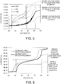
- the horizontal axis represents a voltage applied between the electrode 10 and the backside electrode 9, and the vertical axis represents a current flowing through the photodetector.
- the opening areas of the first light detection element 1 and the second light detection element 2 are substantially the same, and the distance between the elements is also substantially the same.
- the voltage at which the current begins to rise is denoted by a voltage V 1 and the voltage at which the current further sharply rises is denoted by a voltage V 2 .
- the voltage V 1 is the minimum voltage required for photoelectric conversion by the light detection element
- the voltage V 2 is the voltage at which the photoelectric conversion efficiency is the best.
- the driving voltage range tends to become narrow as the number of light detection elements increases.
- the depth of the p + -type semiconductor layer 7 of the second light detection element 2 is shallower than that of the p + -type semiconductor layer 5 of the first light detection element 1. It can be said that there is a tendency that, as the depth of the p + -type semiconductor layer becomes shallower, the voltage V 1 and the voltage V 2 decrease with the driving voltage range remaining substantially unchanged. In addition, it can be understood that the driving voltage range hardly changes even though the depth of the p + -type semiconductor layer changes.
- the voltage V 1 is about 26 V, and the voltage V 2 is about 34 V.
- the voltage V 1 is about 25 V, and the voltage V 2 is about 34 V.
- the voltage V 1 is about 25 V, and the voltage V 2 is about 34 V.
- (b) and (c) are smaller by about 1 V than (a) in voltage V 1 (the range of the voltage between the voltage V 1 of (a) and the voltage V 1 of (b) and (c) is referred to as ⁇ V 1 ). Therefore, it can be said that the photodetectors of (b) and (c) are wider in the driving voltage range.
- the photodetector of (c) includes the light detection elements 1 and 2 having different driving voltage ranges, if the applied voltage is within a range of ⁇ V 1 , the first light detection element 1 is not driven, but the second light detection element 2 is driven. In the range of ⁇ V 1 , since the first light detection element 1 is not driven, the first light detection element 1 serves as a spacer, and even though the second light detection element 2 is driven, the distance between the second light detection elements 2 is separated, so that it is possible to suppress occurrence of noise such as crosstalk.
- the difference between the voltage V 1 and an arbitrary applied voltage of V 1 or more is called an overvoltage.
- an overvoltage For example, in Fig. 4 , when the overvoltage of the first light detection element 1 and the overvoltage of the second light detection element 2 are calculated in a case where the applied voltage is 28 V, the overvoltage of the first light detection element 1 becomes 2 V, and the overvoltage of the second light detection element 2 becomes 3 V. Therefore, the overvoltage of the first light detection element 1 is smaller. As illustrated in Fig. 4 , as the overvoltage is larger, the current flowing through the photodetector easily flows. In a case where noise occurs due to interference between elements that are so adjacent that the current can easily flow, the noise is easily output, so that the crosstalk increases.
- the photodetector of (c) has a wide driving voltage range and can suppress noise such as crosstalk.
- the ratio of the number of the first light detection elements 1 and the number of the second light detection elements 2 is 3 or more and 24 or less.
- the ratio of the number is less than 3
- the proportion of the second light detection elements 2 becomes large, and there is a possibility that noise such as crosstalk occurs due to interference between the second light detection elements 2.
- the ratio of the number is larger than 24, since the number of the second light detection elements 2 is small, the detection error increases. Therefore, when the number ratio is 3 or more and 24 or less, the interference between the second light detection elements 2 is small, and the detection error is also small.
- Fig. 7 is a diagram illustrating a method of manufacturing the photodetector according to the first embodiment.
- the backside electrode 9 is formed on the backside of the high-concentration p-type substrate 11 by chemical vapor deposition (CVD), and the p-type semiconductor layer 12 is formed by epitaxially growing lightly doped p-type silicon on the light incident side.
- CVD chemical vapor deposition
- the p + -type semiconductor layers 5 are formed to be deep in the stacking direction. Subsequently, by implanting boron ions at positions other than the above-mentioned predetermined positions with energy lower than the above-mentioned predetermined energy, the p + -type semiconductor layers 7 are formed to be shallower than the p + -type semiconductor layers 5 in the stacking direction.
- the p + -type semiconductor layers 7 are formed to be shallower than the p + -type semiconductor layers 5 in the stacking direction.
- the second light detection elements 2 are formed so that the distance between the second light detection elements 2 is increased.
- the first light detection elements 1 and the second light detection elements 2 are formed.
- the depths in the stacking direction are different, but since the ion implantation energies of the n + -type semiconductor layers 6 and 8 are substantially the same, the depths are substantially the same.
- the electrode 10 is formed so as to be electrically connected to the n + -type semiconductor layers 6 and 8 by CVD. After that, the mask is removed. In addition, a protective layer 70 is formed by CVD so as to cover the p-type semiconductor layer 12, the first light detection element 1, the second light detection element 2, and the electrode 10.
- the photodetector according to this embodiment can be easily manufactured.
- the photodetector according to the first embodiment has a wide driving voltage range and suppresses noise, so that it is possible to easily manufacture the photodetector.
- the p + -type semiconductor layers 5 and 7 may have different impurity concentrations.
- p type and n type may be reversed.
- Fig. 8 is a diagram illustrating a LIDAR device 5001 according to a second embodiment.
- the LIDAR device 5001 can be applied to long distance subject detection system configured with a line light source and a lens and the like.
- the LIDAR device 5001 includes a light projection unit that projects laser light to a target 501, a light reception unit that receives laser light from the target 501, and a time-of-flight (TOF) distance measurement device (not illustrated) that measures a time when the laser light reciprocates to the target 501 and converts the time into a distance.
- TOF time-of-flight
- a laser light oscillator 304 oscillates laser light.
- a driving circuit 303 drives the laser light oscillator 304.
- the optical system 305 extracts a portion of the laser light as reference light and irradiates the target 501 with the other laser light through a mirror 306.
- a mirror controller 302 controls the mirror 306 to project laser light onto the target 501.
- the light projection denotes hitting with light.
- a reference light photodetector 309 detects the reference light extracted by an optical system 305.
- a photodetector 310 receives reflected light from the target 501.
- a distance measurement circuit 308 measures the distance to the target 501 on the basis of a difference between the time when the reference light photodetector 309 detects the reference light and the time when the photodetector 310 detects the reflected light.
- An image recognition system 307 recognizes the target 501 based on the result measured by the distance measurement circuit 308.
- the LIDAR device 5001 is a distance image sensing system adopting a time-of-flight (TOF) distance measuring method of measuring a time when the laser light reciprocates to the target 501 and converting the time into a distance.
- the LIDAR device 5001 is applied to an in-vehicle drive-assist system, remote sensing, and the like.
- the photodetector according to the first embodiment is used as the photodetector 310, the photodetector exhibits good sensitivity particularly in a near infrared range. For this reason, the LIDAR device 5001 can be applied to a light source in a wavelength band which is invisible to persons.
- the LIDAR device 5001 can be used, for example, for obstacle detection for a vehicle.
- Fig. 9 is a diagram illustrating a measurement system.
- the measurement system includes at least a photodetector 3001 and a light source 3000.
- the light source 3000 of the measurement system emits light 412 to an object 500 to be measured.
- the photodetector 3001 detects the light 413 transmitted through, reflected on, or diffused by the object 500.
- a highly sensitive measurement system is realized by using, for example, the photodetector according to the first embodiment.
Landscapes
- Physics & Mathematics (AREA)
- Engineering & Computer Science (AREA)
- Electromagnetism (AREA)
- Computer Networks & Wireless Communication (AREA)
- General Physics & Mathematics (AREA)
- Radar, Positioning & Navigation (AREA)
- Remote Sensing (AREA)
- Optical Radar Systems And Details Thereof (AREA)
- Light Receiving Elements (AREA)
- Solid State Image Pick-Up Elements (AREA)
- Transforming Light Signals Into Electric Signals (AREA)
Applications Claiming Priority (1)
| Application Number | Priority Date | Filing Date | Title |
|---|---|---|---|
| JP2018054814A JP6862386B2 (ja) | 2018-03-22 | 2018-03-22 | 光検出器、ライダー装置、及び光検出器の製造方法 |
Publications (1)
| Publication Number | Publication Date |
|---|---|
| EP3543733A1 true EP3543733A1 (fr) | 2019-09-25 |
Family
ID=63557290
Family Applications (1)
| Application Number | Title | Priority Date | Filing Date |
|---|---|---|---|
| EP18193685.7A Withdrawn EP3543733A1 (fr) | 2018-03-22 | 2018-09-11 | Photodétecteur, lidar et procédé de fabrication de photodétecteur |
Country Status (3)
| Country | Link |
|---|---|
| US (1) | US11313956B2 (fr) |
| EP (1) | EP3543733A1 (fr) |
| JP (1) | JP6862386B2 (fr) |
Cited By (1)
| Publication number | Priority date | Publication date | Assignee | Title |
|---|---|---|---|---|
| EP3882987A1 (fr) * | 2020-03-19 | 2021-09-22 | Kabushiki Kaisha Toshiba | Détecteur de lumière, système de détection de lumière, dispositif lidar et véhicule |
Families Citing this family (2)
| Publication number | Priority date | Publication date | Assignee | Title |
|---|---|---|---|---|
| US11393870B2 (en) * | 2018-12-18 | 2022-07-19 | Canon Kabushiki Kaisha | Photoelectric conversion device, imaging system, and mobile apparatus |
| CN121619970A (zh) * | 2026-01-29 | 2026-03-06 | 国科大杭州高等研究院 | 雪崩光电探测器及其制备方法 |
Citations (8)
| Publication number | Priority date | Publication date | Assignee | Title |
|---|---|---|---|---|
| US20020195545A1 (en) * | 2001-06-20 | 2002-12-26 | Nishimura Ken A. | Avalanche photodiode array biasing device and avalanche photodiode structure |
| EP2040308A1 (fr) * | 2006-07-03 | 2009-03-25 | Hamamatsu Photonics K.K. | Ensemble photodiode |
| WO2010073137A1 (fr) * | 2008-12-22 | 2010-07-01 | Koninklijke Philips Electronics N.V. | Imageur cmos avec capacité de comptage de photon unique |
| US20130153754A1 (en) * | 2011-12-20 | 2013-06-20 | Stmicroelectronics (Grenoble 2) Sas | Device having spad photodiodes for detecting an object |
| US20140184197A1 (en) * | 2012-12-27 | 2014-07-03 | General Electric Company | Characterization and Calibration of Large Area Solid State Photomultiplier Breakdown Voltage and/or Capacitance |
| US9153608B2 (en) * | 2011-07-04 | 2015-10-06 | Hamamatsu Photonics K.K. | Photodiode array, method for determining reference voltage, and method for determining recommended operating voltage |
| CN106441597A (zh) * | 2016-09-26 | 2017-02-22 | 东南大学 | 一种应用于阵列雪崩二极管的反偏电压调节电路 |
| EP3182154A1 (fr) * | 2015-12-20 | 2017-06-21 | Apple Inc. | Réseau spad avec commande de polarisation au niveau pixel |
Family Cites Families (8)
| Publication number | Priority date | Publication date | Assignee | Title |
|---|---|---|---|---|
| JP3216153B2 (ja) | 1991-07-30 | 2001-10-09 | 株式会社デンソー | 光検出器 |
| JP3304742B2 (ja) | 1996-01-30 | 2002-07-22 | ウシオ電機株式会社 | 紫外光検出器 |
| KR101607356B1 (ko) | 2008-09-03 | 2016-03-29 | 아이아이아이 홀딩스 3, 엘엘씨 | 자기 메모리 소자 및 그것을 이용하는 기억 장치 |
| JP5450295B2 (ja) | 2010-07-05 | 2014-03-26 | オリンパス株式会社 | 撮像装置および撮像装置の製造方法 |
| JP5766062B2 (ja) | 2011-08-05 | 2015-08-19 | キヤノン株式会社 | 軟x線検出装置、及び軟x線検出システム |
| JP2013038174A (ja) | 2011-08-05 | 2013-02-21 | Canon Inc | 軟x線検出装置、及び軟x線検出システム |
| JP6386847B2 (ja) | 2014-09-19 | 2018-09-05 | 浜松ホトニクス株式会社 | 紫外線センサ及び紫外線検出装置 |
| US10324171B2 (en) * | 2015-12-20 | 2019-06-18 | Apple Inc. | Light detection and ranging sensor |
-
2018
- 2018-03-22 JP JP2018054814A patent/JP6862386B2/ja not_active Expired - Fee Related
- 2018-09-11 EP EP18193685.7A patent/EP3543733A1/fr not_active Withdrawn
- 2018-09-12 US US16/129,205 patent/US11313956B2/en active Active
Patent Citations (8)
| Publication number | Priority date | Publication date | Assignee | Title |
|---|---|---|---|---|
| US20020195545A1 (en) * | 2001-06-20 | 2002-12-26 | Nishimura Ken A. | Avalanche photodiode array biasing device and avalanche photodiode structure |
| EP2040308A1 (fr) * | 2006-07-03 | 2009-03-25 | Hamamatsu Photonics K.K. | Ensemble photodiode |
| WO2010073137A1 (fr) * | 2008-12-22 | 2010-07-01 | Koninklijke Philips Electronics N.V. | Imageur cmos avec capacité de comptage de photon unique |
| US9153608B2 (en) * | 2011-07-04 | 2015-10-06 | Hamamatsu Photonics K.K. | Photodiode array, method for determining reference voltage, and method for determining recommended operating voltage |
| US20130153754A1 (en) * | 2011-12-20 | 2013-06-20 | Stmicroelectronics (Grenoble 2) Sas | Device having spad photodiodes for detecting an object |
| US20140184197A1 (en) * | 2012-12-27 | 2014-07-03 | General Electric Company | Characterization and Calibration of Large Area Solid State Photomultiplier Breakdown Voltage and/or Capacitance |
| EP3182154A1 (fr) * | 2015-12-20 | 2017-06-21 | Apple Inc. | Réseau spad avec commande de polarisation au niveau pixel |
| CN106441597A (zh) * | 2016-09-26 | 2017-02-22 | 东南大学 | 一种应用于阵列雪崩二极管的反偏电压调节电路 |
Cited By (1)
| Publication number | Priority date | Publication date | Assignee | Title |
|---|---|---|---|---|
| EP3882987A1 (fr) * | 2020-03-19 | 2021-09-22 | Kabushiki Kaisha Toshiba | Détecteur de lumière, système de détection de lumière, dispositif lidar et véhicule |
Also Published As
| Publication number | Publication date |
|---|---|
| JP2019169793A (ja) | 2019-10-03 |
| JP6862386B2 (ja) | 2021-04-21 |
| US11313956B2 (en) | 2022-04-26 |
| US20190293767A1 (en) | 2019-09-26 |
Similar Documents
| Publication | Publication Date | Title |
|---|---|---|
| JP7328868B2 (ja) | 光検出器、光検出システム、ライダー装置、及び車 | |
| US9691932B2 (en) | Photodetector | |
| JP7039411B2 (ja) | 光検出器、光検出システム、ライダー装置及び車 | |
| EP3544064B1 (fr) | Photodétecteur et détection et télémétrie de la lumière | |
| CN107665886A (zh) | 用于检测红外线辐射的盖革模式雪崩光电二极管阵列 | |
| US11313956B2 (en) | Photodetector, LIDAR, and method of manufactuaring photodetector | |
| KR102774273B1 (ko) | 단일 광자 검출 픽셀 및 이를 포함하는 단일 광자 검출 픽셀 어레이 | |
| US12142616B2 (en) | Light detector, light detection system, LIDAR device, and mobile body | |
| US11189746B2 (en) | Photodetector comprising dual cells with different thickness of interposing substrates, photodetection device, laser imaging detection and ranging apparatus and method of manufacturing a photodetector | |
| JP6975110B2 (ja) | 光検出素子、光検出システム、ライダー装置及び車 | |
| US10782428B1 (en) | Light receiving device and distance measuring apparatus | |
| US20250151429A1 (en) | Single photon avalanche diode | |
| US11139326B2 (en) | Photodetector, photodetection device, laser imaging detection and ranging apparatus | |
| JP6847878B2 (ja) | 光検出器、光検出装置及びライダー装置 | |
| KR20250005020A (ko) | 단일 광자 검출 소자, 전자 장치, 및 라이다 장치 | |
| US20190157479A1 (en) | Photodetection element, photodetector, photodetection system and laser imaging detection and ranging apparatus | |
| US20240072191A1 (en) | Light detector, light detection system, lidar device, and mobile body | |
| JP6975113B2 (ja) | 光検出素子、光検出器、光検出システム、ライダー装置及び車 | |
| US20190088812A1 (en) | Photodetection element, photodetector and laser imaging detection and ranging apparatus | |
| JP7414776B2 (ja) | 光検出器、光検出システム、ライダー装置、及び移動体 | |
| US20260033022A1 (en) | Single photon detection device and electronic device comprising diffraction pattern | |
| US20250040263A1 (en) | SINGLE PHOTON AVALANCHE DIODE, ELECTRONIC DEVICE, AND LiDAR DEVICE | |
| JP7515422B2 (ja) | 光検出器、光検出システム、ライダー装置、及び移動体 | |
| CN114122031A (zh) | 一种传感器及制造方法 |
Legal Events
| Date | Code | Title | Description |
|---|---|---|---|
| PUAI | Public reference made under article 153(3) epc to a published international application that has entered the european phase |
Free format text: ORIGINAL CODE: 0009012 |
|
| STAA | Information on the status of an ep patent application or granted ep patent |
Free format text: STATUS: REQUEST FOR EXAMINATION WAS MADE |
|
| 17P | Request for examination filed |
Effective date: 20180911 |
|
| AK | Designated contracting states |
Kind code of ref document: A1 Designated state(s): AL AT BE BG CH CY CZ DE DK EE ES FI FR GB GR HR HU IE IS IT LI LT LU LV MC MK MT NL NO PL PT RO RS SE SI SK SM TR |
|
| AX | Request for extension of the european patent |
Extension state: BA ME |
|
| STAA | Information on the status of an ep patent application or granted ep patent |
Free format text: STATUS: EXAMINATION IS IN PROGRESS |
|
| 17Q | First examination report despatched |
Effective date: 20200508 |
|
| STAA | Information on the status of an ep patent application or granted ep patent |
Free format text: STATUS: THE APPLICATION IS DEEMED TO BE WITHDRAWN |
|
| 18D | Application deemed to be withdrawn |
Effective date: 20240403 |