EP3547302B1 - Erhöhte pwm-tiefe bei der digitalen ansteuerung von aktivmatrix-displays - Google Patents
Erhöhte pwm-tiefe bei der digitalen ansteuerung von aktivmatrix-displays Download PDFInfo
- Publication number
- EP3547302B1 EP3547302B1 EP18182989.6A EP18182989A EP3547302B1 EP 3547302 B1 EP3547302 B1 EP 3547302B1 EP 18182989 A EP18182989 A EP 18182989A EP 3547302 B1 EP3547302 B1 EP 3547302B1
- Authority
- EP
- European Patent Office
- Prior art keywords
- bit
- time slots
- selection
- sub
- block
- Prior art date
- Legal status (The legal status is an assumption and is not a legal conclusion. Google has not performed a legal analysis and makes no representation as to the accuracy of the status listed.)
- Active
Links
Images












Classifications
-
- G—PHYSICS
- G09—EDUCATION; CRYPTOGRAPHY; DISPLAY; ADVERTISING; SEALS
- G09G—ARRANGEMENTS OR CIRCUITS FOR CONTROL OF INDICATING DEVICES USING STATIC MEANS TO PRESENT VARIABLE INFORMATION
- G09G3/00—Control arrangements or circuits, of interest only in connection with visual indicators other than cathode-ray tubes
- G09G3/20—Control arrangements or circuits, of interest only in connection with visual indicators other than cathode-ray tubes for presentation of an assembly of a number of characters, e.g. a page, by composing the assembly by combination of individual elements arranged in a matrix no fixed position being assigned to or needed to be assigned to the individual characters or partial characters
- G09G3/22—Control arrangements or circuits, of interest only in connection with visual indicators other than cathode-ray tubes for presentation of an assembly of a number of characters, e.g. a page, by composing the assembly by combination of individual elements arranged in a matrix no fixed position being assigned to or needed to be assigned to the individual characters or partial characters using controlled light sources
- G09G3/30—Control arrangements or circuits, of interest only in connection with visual indicators other than cathode-ray tubes for presentation of an assembly of a number of characters, e.g. a page, by composing the assembly by combination of individual elements arranged in a matrix no fixed position being assigned to or needed to be assigned to the individual characters or partial characters using controlled light sources using electroluminescent panels
- G09G3/32—Control arrangements or circuits, of interest only in connection with visual indicators other than cathode-ray tubes for presentation of an assembly of a number of characters, e.g. a page, by composing the assembly by combination of individual elements arranged in a matrix no fixed position being assigned to or needed to be assigned to the individual characters or partial characters using controlled light sources using electroluminescent panels semiconductive, e.g. using light-emitting diodes [LED]
- G09G3/3208—Control arrangements or circuits, of interest only in connection with visual indicators other than cathode-ray tubes for presentation of an assembly of a number of characters, e.g. a page, by composing the assembly by combination of individual elements arranged in a matrix no fixed position being assigned to or needed to be assigned to the individual characters or partial characters using controlled light sources using electroluminescent panels semiconductive, e.g. using light-emitting diodes [LED] organic, e.g. using organic light-emitting diodes [OLED]
- G09G3/3225—Control arrangements or circuits, of interest only in connection with visual indicators other than cathode-ray tubes for presentation of an assembly of a number of characters, e.g. a page, by composing the assembly by combination of individual elements arranged in a matrix no fixed position being assigned to or needed to be assigned to the individual characters or partial characters using controlled light sources using electroluminescent panels semiconductive, e.g. using light-emitting diodes [LED] organic, e.g. using organic light-emitting diodes [OLED] using an active matrix
- G09G3/3258—Control arrangements or circuits, of interest only in connection with visual indicators other than cathode-ray tubes for presentation of an assembly of a number of characters, e.g. a page, by composing the assembly by combination of individual elements arranged in a matrix no fixed position being assigned to or needed to be assigned to the individual characters or partial characters using controlled light sources using electroluminescent panels semiconductive, e.g. using light-emitting diodes [LED] organic, e.g. using organic light-emitting diodes [OLED] using an active matrix with pixel circuitry controlling the voltage across the light-emitting element
-
- G—PHYSICS
- G09—EDUCATION; CRYPTOGRAPHY; DISPLAY; ADVERTISING; SEALS
- G09G—ARRANGEMENTS OR CIRCUITS FOR CONTROL OF INDICATING DEVICES USING STATIC MEANS TO PRESENT VARIABLE INFORMATION
- G09G3/00—Control arrangements or circuits, of interest only in connection with visual indicators other than cathode-ray tubes
- G09G3/20—Control arrangements or circuits, of interest only in connection with visual indicators other than cathode-ray tubes for presentation of an assembly of a number of characters, e.g. a page, by composing the assembly by combination of individual elements arranged in a matrix no fixed position being assigned to or needed to be assigned to the individual characters or partial characters
- G09G3/2003—Display of colours
-
- G—PHYSICS
- G09—EDUCATION; CRYPTOGRAPHY; DISPLAY; ADVERTISING; SEALS
- G09G—ARRANGEMENTS OR CIRCUITS FOR CONTROL OF INDICATING DEVICES USING STATIC MEANS TO PRESENT VARIABLE INFORMATION
- G09G3/00—Control arrangements or circuits, of interest only in connection with visual indicators other than cathode-ray tubes
- G09G3/20—Control arrangements or circuits, of interest only in connection with visual indicators other than cathode-ray tubes for presentation of an assembly of a number of characters, e.g. a page, by composing the assembly by combination of individual elements arranged in a matrix no fixed position being assigned to or needed to be assigned to the individual characters or partial characters
- G09G3/2007—Display of intermediate tones
- G09G3/2018—Display of intermediate tones by time modulation using two or more time intervals
-
- G—PHYSICS
- G09—EDUCATION; CRYPTOGRAPHY; DISPLAY; ADVERTISING; SEALS
- G09G—ARRANGEMENTS OR CIRCUITS FOR CONTROL OF INDICATING DEVICES USING STATIC MEANS TO PRESENT VARIABLE INFORMATION
- G09G3/00—Control arrangements or circuits, of interest only in connection with visual indicators other than cathode-ray tubes
- G09G3/20—Control arrangements or circuits, of interest only in connection with visual indicators other than cathode-ray tubes for presentation of an assembly of a number of characters, e.g. a page, by composing the assembly by combination of individual elements arranged in a matrix no fixed position being assigned to or needed to be assigned to the individual characters or partial characters
- G09G3/2007—Display of intermediate tones
- G09G3/2018—Display of intermediate tones by time modulation using two or more time intervals
- G09G3/2022—Display of intermediate tones by time modulation using two or more time intervals using sub-frames
- G09G3/2025—Display of intermediate tones by time modulation using two or more time intervals using sub-frames the sub-frames having all the same time duration
-
- G—PHYSICS
- G09—EDUCATION; CRYPTOGRAPHY; DISPLAY; ADVERTISING; SEALS
- G09G—ARRANGEMENTS OR CIRCUITS FOR CONTROL OF INDICATING DEVICES USING STATIC MEANS TO PRESENT VARIABLE INFORMATION
- G09G3/00—Control arrangements or circuits, of interest only in connection with visual indicators other than cathode-ray tubes
- G09G3/20—Control arrangements or circuits, of interest only in connection with visual indicators other than cathode-ray tubes for presentation of an assembly of a number of characters, e.g. a page, by composing the assembly by combination of individual elements arranged in a matrix no fixed position being assigned to or needed to be assigned to the individual characters or partial characters
- G09G3/2007—Display of intermediate tones
- G09G3/2018—Display of intermediate tones by time modulation using two or more time intervals
- G09G3/2022—Display of intermediate tones by time modulation using two or more time intervals using sub-frames
- G09G3/2033—Display of intermediate tones by time modulation using two or more time intervals using sub-frames with splitting one or more sub-frames corresponding to the most significant bits into two or more sub-frames
-
- G—PHYSICS
- G09—EDUCATION; CRYPTOGRAPHY; DISPLAY; ADVERTISING; SEALS
- G09G—ARRANGEMENTS OR CIRCUITS FOR CONTROL OF INDICATING DEVICES USING STATIC MEANS TO PRESENT VARIABLE INFORMATION
- G09G3/00—Control arrangements or circuits, of interest only in connection with visual indicators other than cathode-ray tubes
- G09G3/20—Control arrangements or circuits, of interest only in connection with visual indicators other than cathode-ray tubes for presentation of an assembly of a number of characters, e.g. a page, by composing the assembly by combination of individual elements arranged in a matrix no fixed position being assigned to or needed to be assigned to the individual characters or partial characters
- G09G3/22—Control arrangements or circuits, of interest only in connection with visual indicators other than cathode-ray tubes for presentation of an assembly of a number of characters, e.g. a page, by composing the assembly by combination of individual elements arranged in a matrix no fixed position being assigned to or needed to be assigned to the individual characters or partial characters using controlled light sources
- G09G3/30—Control arrangements or circuits, of interest only in connection with visual indicators other than cathode-ray tubes for presentation of an assembly of a number of characters, e.g. a page, by composing the assembly by combination of individual elements arranged in a matrix no fixed position being assigned to or needed to be assigned to the individual characters or partial characters using controlled light sources using electroluminescent panels
- G09G3/32—Control arrangements or circuits, of interest only in connection with visual indicators other than cathode-ray tubes for presentation of an assembly of a number of characters, e.g. a page, by composing the assembly by combination of individual elements arranged in a matrix no fixed position being assigned to or needed to be assigned to the individual characters or partial characters using controlled light sources using electroluminescent panels semiconductive, e.g. using light-emitting diodes [LED]
- G09G3/3208—Control arrangements or circuits, of interest only in connection with visual indicators other than cathode-ray tubes for presentation of an assembly of a number of characters, e.g. a page, by composing the assembly by combination of individual elements arranged in a matrix no fixed position being assigned to or needed to be assigned to the individual characters or partial characters using controlled light sources using electroluminescent panels semiconductive, e.g. using light-emitting diodes [LED] organic, e.g. using organic light-emitting diodes [OLED]
- G09G3/3266—Details of drivers for scan electrodes
-
- G—PHYSICS
- G09—EDUCATION; CRYPTOGRAPHY; DISPLAY; ADVERTISING; SEALS
- G09G—ARRANGEMENTS OR CIRCUITS FOR CONTROL OF INDICATING DEVICES USING STATIC MEANS TO PRESENT VARIABLE INFORMATION
- G09G2310/00—Command of the display device
- G09G2310/02—Addressing, scanning or driving the display screen or processing steps related thereto
- G09G2310/0264—Details of driving circuits
- G09G2310/0286—Details of a shift registers arranged for use in a driving circuit
-
- G—PHYSICS
- G09—EDUCATION; CRYPTOGRAPHY; DISPLAY; ADVERTISING; SEALS
- G09G—ARRANGEMENTS OR CIRCUITS FOR CONTROL OF INDICATING DEVICES USING STATIC MEANS TO PRESENT VARIABLE INFORMATION
- G09G2310/00—Command of the display device
- G09G2310/06—Details of flat display driving waveforms
- G09G2310/061—Details of flat display driving waveforms for resetting or blanking
-
- G—PHYSICS
- G09—EDUCATION; CRYPTOGRAPHY; DISPLAY; ADVERTISING; SEALS
- G09G—ARRANGEMENTS OR CIRCUITS FOR CONTROL OF INDICATING DEVICES USING STATIC MEANS TO PRESENT VARIABLE INFORMATION
- G09G2320/00—Control of display operating conditions
- G09G2320/04—Maintaining the quality of display appearance
- G09G2320/043—Preventing or counteracting the effects of ageing
Definitions
- the present invention relates to the field of digital driving of displays. More specifically it relates to methods for digitally driving active matrix displays, for instance AMOLED (Active Matrix Organic Light Emitting Diode) displays, so as to obtain high color accuracy, and to digital driving circuitry for active matrix displays, for instance AMOLED displays, providing high color accuracy.
- AMOLED Active Matrix Organic Light Emitting Diode
- Prior art backplanes for AMOLED displays use a pixel driver circuit for each OLED, each pixel driver circuit driving a predetermined current through the corresponding OLED.
- Multiple pixel driver circuit schematics are being implemented, which all comprise a drive transistor (such as M1 in FIG. 1 ) driving the predetermined current through the OLED.
- an amplitude modulation approach is used, wherein each OLED emits light during a full frame period with an intensity corresponding to the required gray level.
- the current through the OLED is determined in accordance with an analog data voltage on the floating gate of the drive transistor M1.
- this transistor M1 preferably operates in saturation for accurate current control, the current through the OLED (and thus the OLED luminance) varies with the square of the M1 gate voltage. This introduces non-linearity in the display response, limits accuracy and makes the display sensitive to noise.
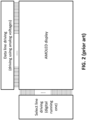
- An overall display architecture as schematically shown in FIG. 2 is currently used for analog driven displays. At one edge of the display, a select line driver integrated circuit is provided.
- the select lines are digitally driven, for instance by a running one, cycling at a rate corresponding to the frame rate.
- data line driver circuitry is provided for driving the data lines.
- the data lines are driven by an analog voltage, keeping the pixels at a constant luminance during an entire image frame.
- a Pulse Width Modulation approach can be used, wherein each OLED emits light during a portion of a frame period, at a single luminance.
- the portion of the frame period during which an OLED emits light has a duration corresponding to the required gray level.
- a pulse current having a duty ratio in accordance with the data voltage is supplied to each OLED.
- a frame is divided into n sub-frames, wherein n is the number of bits used for digitally representing the image data. These n sub-frames may have a different duration, there being a ratio 1:2:4:8:....:2 n-1 between the different sub-frame durations.
- a pixel In each sub-frame a pixel (OLED) is either ON or OFF. In this way 2 n different gray levels can be created.
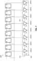
- a display architecture is used wherein select lines (for instance rows) are digitally driven by dedicated timing control circuitry and wherein data lines (for instance columns) are driven by a digital voltage, as schematically illustrated in FIG. 3 .
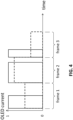
- FIG. 4 shows a comparison between a typical analog pixel driving method (dashed lines) and a digital pixel driving method (full lines).
- an analog driven pixel the pixel luminance is constant during each image frame period and it can be different from frame to frame.
- the pixel luminance can have 2 n different levels.
- a digital driven pixel a pixel is at full luminance(ON) during part of a frame period and at zero luminance (OFF) during the remaining part of the frame period.
- FIG. 4 is only a schematic representation, not showing a division in sub-frames for the digital driving approach.
- WO 2014/068017 describes a method and digital driving circuitry for digital driving of an active matrix display with a predetermined frame rate, by means of pulse width modulation (PWM).
- PWM pulse width modulation
- the described method includes representing each of the plurality of pixels of an image to be displayed within a frame by an n-bit digital code.
- the image frame is divided into sub-frames, which may be of substantially equal duration.
- the method includes sequentially selecting at least one of the plurality of rows twice. Upon a first selection, a first digital code is written to the selected row, and upon a second selection, a second digital code is written to the selected row.
- This alternation of driving between both lines causes that the line driven first is typically half a time unit longer active than the other line.
- One way to avoid this half time unit difference is to swap the sequence of both lines during the next image frame, such that on average they have equal length.
- this implementation is not preferred, because it again gives a variation at half the frame refresh rate, which leads to possible subharmonics (e.g. a 30 Hz signal component in a display driven at 60 Hz), which may lead to causing flickering and hence should be avoided.
- OLED displays are displays comprising an array of light-emitting diodes in which the emissive electroluminescent layer is a film of organic compound which emits light in response to an electric current.
- OLED displays can either use passive-matrix (PMOLED) or active-matrix (AMOLED) addressing schemes.
- PMOLED passive-matrix
- AMOLED active-matrix
- the present invention relates to AMOLED displays.
- the corresponding addressing scheme makes use of a thin-film transistor backplane to switch each individual OLED pixel on or off.
- AMOLED displays allow for higher resolution and larger display sizes than PMOLED displays.
- the present invention is not limited to AMOLED displays, but in a broader concept relates to active matrix displays. Any type of active matrix displays may use the concepts of embodiments of the present invention, although AMOLED displays are particularly advantageous in view of the current switching speeds of their pixel elements. It is advantageous if the pixel elements of the active matrix displays can switch faster, as this allows to obtain higher frame rates, hence less flickering images.
- An active matrix display e.g. an AMOLED display, according to embodiments of the present invention comprises a plurality of pixels, each comprising a pixel element, e.g. an OLED element.
- the pixel elements are arranged in an array, and are logically organised in rows and columns.
- horizontal and vertical are used to provide a co-ordinate system and for ease of explanation only. They do not need to, but may, refer to an actual physical direction of the device.
- the terms “column” and “row” or “line” are used to describe sets of array elements which are linked together.
- the linking can be in the form of a Cartesian array of lines and columns; however, the present invention is not limited thereto. As will be understood by those skilled in the art, columns and lines can be easily interchanged and it is intended in this disclosure that these terms be interchangeable. Also, non-Cartesian arrays may be constructed and are included within the scope of the invention. Accordingly the terms "row” or “line” and “column” should be interpreted widely. To facilitate in this wide interpretation, the claims refer to logically organised in rows and columns. By this is meant that sets of pixel elements are linked together in a topologically linear intersecting manner; however, that the physical or topographical arrangement need not be so.
- the rows may be circles and the columns radii of these circles and the circles and radii are described in this invention as "logically organised" rows and columns.
- specific names of the various lines e.g. select line and data line, are intended to be generic names used to facilitate the explanation and to refer to a particular function and this specific choice of words is not intended to in any way limit the invention. It should be understood that all these terms are used only to facilitate a better understanding of the specific structure being described, and are in no way intended to limit the invention.
- selection in “first selection” and “second selection”
- action in the circuit that enables data to be introduced. This could be, for example, multiplying a bit from a data code by one in a logical implementation. Alternatively, it may be seen as running a one in a select line of a circuit, changing the state of a transistor to introduce data from a data line.
- a first selection followed by a second selection may comprise introducing data a first time, followed by introducing data a second time.
- a frame is a single picture or single image that is shown as part of a sequence of pictures.
- the frame rate or frame frequency is the rate or frequency at which consecutive images (frames) are formed and displayed.
- the frame period (fp) is a time interval equal to the reciprocal of the frame frequency. It corresponds to the display period of a single frame or image.
- a frame can be divided into sub-frames.
- each pixel is addressed once each frame.
- different pulse with different lengths are needed to obtain the different grey scales.
- the different timing moments to drive a pixel are grouped into sub-frames.
- the sub-frames which together form a frame each have a subframe duration which lasts for only part of the total frame period; the sum of these parts of all sub-frames together forming a frame being equal to one frame period.
- Pixels in the frame which are very bright may give a lot of intensity in all sub-frames, while pixels which are less bright may give more intensity in some sub-frames, and less intensity in other sub-frames, and pixels which are very dark may give little intensity in all sub-frames.
- the duration of each of the sub-frames of a frame may be, but does not have to be, substantially equal. In those embodiments in which each sub-frame duration is substantially equal, each frame, which has a duration of one frame period fp, may be divided in N sub-frames with a duration of fp/N. Nonetheless, the present invention is not limited by equal duration of the sub-frames.
- the present invention relates to methods for digital driving of pixels of active matrix displays, for instance AMOLED displays, with a predetermined frame rate.
- the display comprises a plurality of pixels logically organized in a plurality of rows and columns.
- the method comprises representing each of the plurality of pixels of an image to be displayed within a frame by an n-bit digital image code, and dividing the image into a natural number N (>1) of sub-frames. Each sub-frame is further divided into time slots, and a number of time slots are assigned to each bit of the n-bit image code according to each bit's significance in the code.
- the method further comprises selecting each of the plurality of rows one first time per sub-frame, and subsequently for at least one sub-frame, a second time. This implies that at least one sub-frame will be sequentially selected twice.
- Data code corresponding to pixel data of image pixels to be represented and, in some embodiments, dummy data or reset data (a zero) is introduced with each selection.
- this sequence of first selection and second selection takes place in at least 35% of the sub-frames, or in at least half of the sub-frames. In certain embodiments, at least 75%, 80% or even more than 90% of sub-frames are selected twice.
- the first selection and the second selection are performed sequentially for at least one and preferably more of the sub-frames. This means that there is a time delay between the first selection and the second selection, and this time delay may be different for each sub-frame.
- the time delay in at least one of the sub-frames may equal 1 more or 1 less than 1/2 N-x of the sub-frame duration.
- the data introduced in each sub-frame is the bits in order from the least significant bit LSB to the most significant bit MSB.
- a frame is divided into 2 n time slots, from which only 2 n -1 time slots are used for effective driving. There remains one time slot that is unused.
- the present invention will use that one unused time slot for improving the driving scheme.
- each sub-frame may be considered with the same duration.
- Each sub-frame is divided in time slots, which may also have the same duration.
- each bit is assigned to a number of time slots according to their position, so the m th bit (1 ⁇ m ⁇ n), the first bit being the LSB and the n-th bit being the MSB, will be assigned to 2 m-1 time slots.
- the introduction of the data is performed twice per sub-frame, for instance according to Table 1. Each of the first three sub-frames are run with two selections.
- the first sub-frame is run with a zero for one time slot, the rest of the sub-frame is run with data bit B4.
- the second sub-frame is run with two selections, one time slot for bit B0, and the remaining three time slots for B4.
- the third sub-frame is selected twice, the first 2 time slots for driving bit B1, the second 2 time slots for driving B4.
- the remainder of the sub-frames are selected only once, for the bits B2, B3 and B4, the second selection not being needed. This way, all bits are represented longer according to their significance in the data code, and this in a homogeneous way, and utilizing most of the time slots (most of the frame) for driving data in the pixel.
- each sub-frame may be considered with the same duration.
- Each sub-frame is divided in time slots, which may also have the same duration.
- each bit is assigned to a number of time slots according to their position, so the m th bit (1 ⁇ m ⁇ n), the first bit being the LSB and the n-th bit being the MSB, will be assigned to 2 m-1 time slots.
- bit B9 will be assigned 512 time slots
- B8 will be assigned 256 time slots
- B7 will be assigned 128 time slots
- B6 will be assigned 64 time slots
- B5 will be assigned 32 time slots
- B4 will be assigned 16 time slots
- B3 will be assigned to 8 time slots
- B2 will be assigned to 4
- each sub-frame may be considered with the same duration.
- Each sub-frame is divided in time slots, which may also have the same duration.
- each bit is assigned to a number of time slots according to their position, so the m th bit (1 ⁇ m ⁇ n), the first bit being the LSB and the n-th bit being the MSB, will be assigned to 2 m-1 time slots.
- a data code with 12 bits may be represented as B11 B10 B9 B8 B7 B6 B5 B4 B3 B2 B1 B0, the MSB bit B11 and LSB B0. The introduction of the data is performed twice per sub-frame, for instance according to Table 3.
- the coding method according to embodiments of the present invention is explained in more detail.
- the remaining unused time slot is used as an additional minimal length block (length 1).
- This block is indicated CX in Table 4 below.
- each of the bits will be assigned to a number of time slots according to their position, with bits closer to the LSB bit having less time slots assigned than bits closer to the MSB.
- a difference compared to the method described in WO 2014/068017 is that the number of time slots assigned to a bit value now no longer is a power of 2, but deviates therefrom.
- the most significant bits are implemented as in the prior art, with the number of time slots assigned being a power of 2 of the value of the position of that bit in the image code.
- the first least significant bit is assigned 1 time slot.
- the further least significant bits are assigned a number of time slots which is larger than the number of time slots (larger than 2 m-1 for the m th bit) which would be assigned if a power of 2 of the value of the position of that bit in the image code would be taken, and the middle significant bits are assigned a number of time slots which is smaller than the number of time slots (smaller than 2 m-1 for the m th bit) which would be assigned if a power of 2 of the value of the position of that bit in the image code would be taken.
- each subframe comprises maximal (any multiple of) 128 lines.
- Each image comprises in this approach typically 128 lines. If the image consists of more than 128 lines, the lines are grouped in blocks. e.g. a display of 1000 lines will be driven with this code as 128 blocks of 8 lines.
- Driving each subframe comprises driving maximum 2 pulses of in total 256 timeslots.
- Time slots acc to prior art 1 2 4 8 16 32 64 128 256 512 1024 2048 Bit number B0 B1 B2 B3 B4 B5 B6 B7 B8 B9 B10 B11
- the number of time slots assigned to each bit value can be as follows: Time slots acc to invention 1 3 5 11 15 31 63 127 255 512 1024 2048 1 Bit number C0 C1 C2 C3 C4 C5 C6 C7 C8 C9 C10 C11 CX
- the least significant bit B0 is assigned 1 time slot (indicated by C0)
- bit B2 is assigned 5 time slots
- bit B3 is assigned 11 time slots.
- bits C1 to C3 are the ones being assigned more time slots than would have been the case in the prior art.
- the number of time slots assigned to the least significant bits should always be uneven.
- the middle significant bits B4 to B8 each are assigned less time slots, for instance one time slot less, than would have been the case in the prior art.
- the number of time slots assigned to the middle significant bits can be uneven.
- the most significant bits B9 to B11 are implemented just at their actual value according to their position in the code, if a power of 2 is taken.
- the assigning of the number of time slots to each of the bit values must be such that all intensity values can be covered. In accordance with embodiments of the present invention, this can be done by assigning a value 1 to the otherwise unused time slot CX.
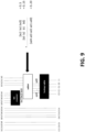
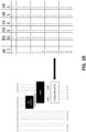
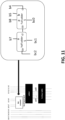
- the coding table may be implemented as illustrated in FIG. 8 to FIG. 10 .
- the driving bits which code the same amount of time slots as if they would have been coded in a prior art power of 2 coding or less, i.e. in this embodiment C11, C10, C9, ..., C5, C4 are directly connected to the input bits B11, B10, B9, ..., B5, B4.
- the driving bits C8, C7, C6, C5, C4 are each one time slot short compared to the time slots that would be assigned in the prior art. Hence 5 time slots need to be compensated for in the least significant bits.
- the active bits in this range having 1 time slot short are counted, B3 B2 B1 B0 (input) covers [0 ...
- C3 C2 C1 C0 covers [0 ... 21].
- CX has a value 1 or 0, to be able to compensate for the lacking time slots, as illustrated in FIG. 10 .
- One implementation of a coding table for this example may be as illustrated in Table 4.
- the first column gives the definition in old time slots, corresponding to the shifting of the line.
- the last two columns give the definition in terms of new time slots, taking into account the additional delay between driving the 1st line and the second line.
- the second and the third column give the value of the code driven in each of the blocks, respectively.
- the proposed value for the first subframe is 128. This means that the bit C10 is run for 256 time slots upon the first selection, and that no second selection is required.
- the proposed values are 0 for the first selection and 128 for the second selection. This means that the bit C0 is run for 1 time slot upon the first selection, and the bit C11 is run for 255 time slots upon the second selection.
- a 9-bit input string may be coded as if it were an 8-bit input string.
- 8 subframes are used.
- Each subframe comprises maximal (any multiple of) 32 lines
- Each image comprises in this approach typically 32 lines. If the image consists of more than 32 lines, the lines are grouped in blocks. e.g. a display of 1000 lines will be driven with this code as 32 blocks of 32 lines, whereas the last 24 lines are virtual lines.
- Driving each subframe comprises driving maximum 2 pulses of in total 64 timeslots.
- the 9-bit input code may have a binary representation B8 B7 B6 B5 B4 B3 B2 B1 B0.
- Time slots acc to prior art 1 2 4 8 16 32 64 128 256 Bit number B0 B1 B2 B3 B4 B5 B6 B7 B8 the number of time slots assigned to each bit value can be as follows: Time slots acc to invention 1 3 5 11 15 31 64 126 255 1 Bit number C0 C1 C2 C3 C4 C5 C6 C7 C8 CX
- bit B0 is assigned 1 time slot (indicated by C0)
- bit B2 is assigned 5 time slots
- bit B3 is assigned 11 time slots.
- bits C1 to C3 are being assigned more time slots than would have been the case in the prior art.
- the number of time slots assigned to the least significant bits is uneven.
- the middle significant bits B4, B5 and the most significant bits B7, B8 each are assigned less time slots, for instance one time slot less for B4, B5 and B8 (indicated C4, C5 and C8), and 2 time slots less for B7 (indicated C7), than would have been the case in the prior art.
- An intermediate significant bit between the middle significant bits and the most significant bit, B6 is implemented just at its actual value according to its position in the code, if a power of 2 is taken.
- the assigning of the number of time slots to each of the bit values (e.g. more than 2 m-1 for at least one of the least significant bits, in this embodiment is less than 2 m-1 for at least one of the middle significant bits and for at least one of the most significant bits, and exactly 2 m-1 for an intermediate significant bits, m being the position of the corresponding bit in the image code) must be such that all intensity values can be covered. In accordance with embodiments of the present invention, this can be done by assigning a value 1 to the otherwise unused time slot CX.
- the coding table may be implemented as illustrated in FIG. 11 to FIG. 13 .
- the driving bits which code the same amount of time slots as if they would have been coded in a prior art power of 2 coding or less, i.e. in this embodiment C8, C7, C6, C5, C4 are directly connected to the input bits B8, B7, B6, B5, B4.
- the driving bits C8, C5, C4 are each one time slot short compared to the time slots that would be assigned in the prior art, and C7 is two time slots short. Hence 5 time slots need to be compensated for in the least significant bits.
- the active bits in this range having time slots short are counted, B3 B2 B1 B0 (input) covers [0 ... 15].
- C3 C2 C1 C0 covers [0 ... 21].
- CX has a value 1 or 0, to be able to compensate for the lacking time slots, as illustrated in FIG. 12 .
- One implementation of a coding table for this example may be as illustrated in Table 5.
- the first column gives the definition in old time slots, corresponding to the shifting of the line.
- the last two columns give the definition in terms of new time slots, taking into account the additional delay between driving the 1st line and the second line.
- the second and the third column give the value of the code driven in each of the blocks, respectively.
- the proposed values for the first subframe are 0 for the first selection and 32 for the second selection. This means that the bit C0 is run for 1 time slot upon the first selection, and that during a second selection the bit C7 is run for 63 time slots.
- the proposed values are 1 for the first selection and 31 for the second selection. This means that the bit C1 is run for 3 time slots upon the first selection, and the bit C8 is run for 61 time slots upon the second selection.
- Each subframe comprises maximal (any multiple of) 256 lines.
- Each image comprises in this approach typically 256 lines. If there are less lines in the display, virtual lines are added up to 256 lines. In the timing they are considered to be present, but they are not actually driven. If the image consists of more than 256 lines, the lines are grouped in blocks. e.g. a display of 1000 lines will be driven with this code as 256 blocks of 4 lines.
- Driving each subframe comprises driving maximum 2 pulses of in total 512 timeslots.
- Time slots acc to prior art 1 2 4 8 16 32 64 128 256 512 1024 2048 4096 Bit number B0 B1 B2 B3 B4 B5 B6 B7 B8 B9 B10 B11 B12
- the number of time slots assigned to each bit value can be as follows: Time slots acc to invention 1 3 5 11 15 31 63 127 255 512 1024 2048 4096 1 Bit number C0 C1 C2 C3 C4 C5 C6 C7 C8 C9 C10 C11 C12 CX
- bit B0 is assigned 1 time slot (indicated by C0)
- bit B2 is assigned 5 time slots
- bit B3 is assigned 11 time slots.
- bits C1 to C3 are the ones being assigned more time slots than would have been the case in the prior art.
- the number of time slots assigned to the least significant bits should always be uneven.
- the middle significant bits B4 to B8 each are assigned less time slots, for instance one time slot less, than would have been the case in the prior art.
- the number of time slots assigned to the middle significant bits in this embodiment can be uneven.
- the most significant bits B9 to B12 are implemented just at their actual value according to their position in the code, if a power of 2 is taken.
- the assigning of the number of time slots to each of the bit values must be such that all intensity values can be covered. In accordance with embodiments of the present invention, this can be done by assigning a value 1 to the otherwise unused time slot CX.
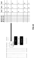
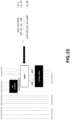
- the coding table may be implemented as illustrated in FIG. 14 to FIG. 16 .
- the driving bits which code the same amount of time slots as if they would have been coded in a prior art power of 2 coding or less, i.e. in this embodiment C12, C11, C10, C9, ..., C5, C4 are directly connected to the input bits B12, B11, B10, B9, ..., B5, B4.
- the driving bits C8, C7, C6, C5, C4 are each one time slot short compared to the time slots that would be assigned in the prior art. Hence 5 time slots need to be compensated for in the least significant bits. As illustrated in FIG.
- B3 B2 B1 B0 (input) covers [0 ... 15].
- the needed range to be covered for compensating for the 5 time slots which are short in the middle significant bits is the sum of both, as illustrated in FIG.15 , hence [0 ... 20].
- C3 C2 C1 C0, including the extra CX covers [0 ... 21].
- CX has a value 1 or 0, to be able to compensate for the lacking time slots, as illustrated in FIG. 16 .
- One implementation of a coding table for this example may be as illustrated in Table 6.
- the first column gives the definition in old time slots, corresponding to the shifting of the line.
- the last two columns give the definition in terms of new time slots, taking into account the additional delay between driving the 1st line and the second line.
- the second and the third column give the value of the code driven in each of the blocks, respectively.
- the proposed values for the first subframe are 0 for the first selection and 256 for the second selection. This means that the bit CX is run for 1 time slot upon the first selection, and that during a second selection the bit C12 is run for 511 time slots.
- the proposed values are again 0 for the first selection and 256 for the second selection. This means that the bit C0 is run for 1 time slot upon the first selection, and the bit C12 is run for 511 time slots upon the second selection.
- the proposed values for the third subframe are 1 for the first selection and 255 for the second selection. This means that the bit C1 is run for 3 time slots upon the first selection, and the bit C12 is run for 509 time slots upon the second selection.
- an additional bit of color depth may be obtained, without having to increase the data rate.
- the demanded driver speed is only half the prior art implementation for an equal color depth.
- Each subframe comprises maximal (any multiple of) 512 lines.
- Each image comprises in this approach typically 512 lines. If there are less lines in the display, virtual lines are added up to 512 lines. In the timing they are considered to be present, but they are not actually driven. If the image consists of more than 512 lines, the lines are grouped in blocks. e.g. a display of 1000 lines will be driven with this code as 512 blocks of 2 lines, whereas the last 24 lines are virtual lines.
- Driving each subframe comprises driving maximum 2 pulses of in total 1024 timeslots.
- the number of time slots assigned to each bit value can be as follows: Time slots acc to invention 1 3 5 11 17 31 63 127 255 511 Bit number C0 C1 C2 C3 C4 C5 C6 C7 C8 C9 Time slots acc to invention 1024 2048 4096 8191 1 Bit number C10 C11 C12 C13 CX
- bits B1, B2, B3, B4 are assigned 3, 5, 11, 17 time slots, respectively (indicated by C1, C2, C3, C4).
- bits C1 to C4 are the ones being assigned more time slots than would have been the case in the prior art.
- the number of time slots assigned to the least significant bits is uneven.
- the middle significant bits B5 to B9 and the most significant bit B13 each are assigned less time slots, for instance one time slot less, than would have been the case in the prior art.
- the number of time slots assigned to the middle significant bits and to the most significant bit in this embodiment is uneven.
- the most significant bits B10 to B12 are implemented just at their actual value according to their position in the code, if a power of 2 is taken.
- the assigning of the number of time slots to each of the bit values must be such that all intensity values can be covered. In accordance with embodiments of the present invention, this can be done by assigning a value 1 to the otherwise unused time slot CX.
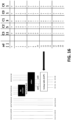
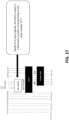
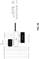
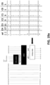
- the coding table may be implemented as illustrated in FIG. 17 , FIG. 18 , FIG. 19a and FIG. 19b .
- the driving bits which code the same amount of time slots as if they would have been coded in a prior art power of 2 coding or less, i.e. in this embodiment C13, C12, C11, C10, C9, ..., C5 are directly connected to the input bits B13, B12, B11, B10, B9, ..., B5.
- the driving bits C13, C9, C8, C7, C6, C5 are each one time slot short compared to the time slots that would be assigned in the prior art. Hence 6 time slots need to be compensated for in the least significant bits. As illustrated in FIG.
- One implementation of a coding table for this example may be as illustrated in Table 7.
- the first column gives the definition in old time slots, corresponding to the shifting of the line.
- the last two columns give the definition in terms of new time slots, taking into account the additional delay between driving the 1st line and the second line.
- the second and the third column give the value of the code driven in each of the blocks, respectively.
- each subframe comprises maximal (any multiple of) 1024 lines.
- Each image comprises in this approach typically 1024 lines. If there are less lines in the display, virtual lines are added up to 1024 lines. In the timing they are considered to be present, but they are not actually driven. If the image consists of more than 1024 lines, the lines are grouped in blocks. e.g. a display of 4000 lines will be driven with this code as 1024 blocks of 4 lines, whereas the last 96 lines are virtual lines.
- Driving each subframe comprises driving maximum 2 pulses of in total 2048 timeslots.
- Time slots acc to prior art 1 2 4 8 16 32 64 128 256 512 1024 Bit number B0 B1 B2 B3 B4 B5 B6 B7 B8 B9 B10
- Time slots acc to prior art 2048 4096 8192 16384 Bit number B11 B12 B13 B14
- the number of time slots assigned to each bit value can be as follows: Time slots acc to invention 1 3 5 11 19 31 63 127 255 511 1023 Bit number C0 C1 C2 C3 C4 C5 C6 C7 C8 C9 C10 Time slots acc to invention 2048 4096 8191 16383 1 Bit number C11 C12 C13 C14 CX
- bits B1, B2, B3, B4 are assigned 3, 5, 11, 19 time slots, respectively (indicated by C1, C2, C3, C4).
- bits C1 to C4 are the ones being assigned more time slots than would have been the case in the prior art.
- the number of time slots assigned to the least significant bits is uneven.
- the middle significant bits B5 to B10 and the most significant bits B13 and B14 each are assigned less time slots, for instance one time slot less, than would have been the case in the prior art.
- the number of time slots assigned to the middle significant bits and to the most significant bits in this embodiment is uneven.
- the intermediate significant bits B11 and B12 between the middle significant bits and the most significant bits are implemented just at their actual value according to their position in the code, if a power of 2 is taken.
- the assigning of the number of time slots to each of the bit values must be such that all intensity values can be covered. In accordance with embodiments of the present invention, this can be done by assigning a value 1 to the otherwise unused time slot CX.
- the coding table may be implemented as illustrated in FIG. 20 , FIG. 21 , FIG. 22a and FIG. 22b .
- the driving bits which code the same amount of time slots as if they would have been coded in a prior art power of 2 coding or less, i.e. in this embodiment C14, C13, C10, C9, ..., C5 are directly connected to the input bits B14, B13, B10, B9, ..., B5.
- the driving bits C14, C13, C10, C9, C8, C7, C6, C5 are each one time slot short compared to the time slots that would be assigned in the prior art. Hence 8 time slots need to be compensated for in the least significant bits. As illustrated in FIG.
- One implementation of a coding table for this example may be as illustrated in Table 8.
- the first column gives the definition in old time slots, corresponding to the shifting of the line.
- the last two columns give the definition in terms of new time slots, taking into account the additional delay between driving the 1st line and the second line.
- the second and the third column give the value of the code driven in each of the blocks, respectively.
- each subframe comprises maximal (any multiple of) 2048 lines.
- Each image comprises in this approach typically 2048 lines. If there are less lines in the display, virtual lines are added up to 2048 lines. In the timing they are considered to be present, but they are not actually driven. If the image consists of more than 2048 lines, the lines are grouped in blocks. e.g. a display of 4000 lines will be driven with this code as 2048 blocks of 2 lines, whereas the last 96 lines are virtual lines.
- Driving each subframe comprises driving maximum 2 pulses of in total 4096 timeslots.
- Time slots acc to prior art 1 2 4 8 16 32 64 128 256 512 1024 2048 Bit number B0 B1 B2 B3 B4 B5 B6 B7 B8 B9 B10 B11
- the number of time slots assigned to each bit value can be as follows: Time slots acc to invention 1 3 5 11 21 31 63 127 255 511 1023 2047 Bit number C0 C1 C2 C3 C4 C5 C6 C7 C8 C9 C10 C11 Time slots acc to invention 4096 8191 16383 32767 1 Bit number C12 C13 C14 C15 CX
- bits B1, B2, B3, B4 are assigned 3, 5, 11, 21 time slots, respectively (indicated by C1, C2, C3, C4).
- bits C1 to C4 are the ones being assigned more time slots than would have been the case in the prior art.
- the number of time slots assigned to the least significant bits is uneven.
- the middle significant bits B5 to B11 and the most significant bits B13 to B15 each are assigned less time slots, for instance each one time slot less, than would have been the case in the prior art.
- the number of time slots assigned to the middle significant bits and to the most significant bits in this embodiment is uneven.
- the intermediate significant bit B12 between the middle significant bits and the most significant bits is implemented just at its actual value according to its position in the code, if a power of 2 is taken.
- the assigning of the number of time slots to each of the bit values must be such that all intensity values can be covered. In accordance with embodiments of the present invention, this can be done by assigning a value 1 to the otherwise unused time slot CX.
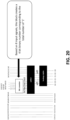
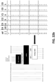
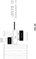
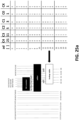
- the coding table may be implemented as illustrated in FIG. 23 , FIG. 24 , FIG. 25a and FIG. 25b .
- the driving bits which code the same amount of time slots as if they would have been coded in a prior art power of 2 coding or less, i.e. in this embodiment C15, C14, C13, C10, C9, ..., C5 are directly connected to the input bits B15, B14, B13, B10, B9, ..., B5.
- the driving bits C15, C14, C13, C10, C9, C8, C7, C6, C5 are each one time slot short compared to the time slots that would be assigned in the prior art. Hence 10 time slots need to be compensated for in the least significant bits. As illustrated in FIG.
- B4 B3 B2 B1 B0 (input) covers [0 ... 31].
- the needed range to be covered for compensating for the 10 time slots which are short in the middle significant bits and most significant bits is the sum of both, as illustrated in FIG.24 , hence [0 ... 41].
- C4 C3 C2 C1 C0, including the extra CX covers [0 ... 42].
- CX has a value 1 or 0, to be able to compensate for the lacking time slots, as illustrated in FIG. 25a and FIG. 25b .
- One implementation of a coding table for this example may be as illustrated in Table 9.
- the first column gives the definition in old time slots, corresponding to the shifting of the line.
- the last two columns give the definition in terms of new time slots, taking into account the additional delay between driving the 1st line and the second line.
- the second and the third column give the value of the code driven in each of the blocks, respectively.
- FIG. 5 schematically shows a digital driven AMOLED display architecture 50, as a particular type of active matrix display, in accordance with an aspect of the present invention.
- This architecture 50 comprises an AMOLED display 55 comprising an array of OLED pixel elements (not illustrated in detail in FIG. 5 ) logically organised in rows and columns.
- the driving circuitry for driving these OLED pixel elements is based on digital select line (row) driving circuitry 51 using two select signals for at least one of the rows, for instance implemented by running ones, and digital data line (column) driving circuitry 52.
- Digital driving can be done for instance using Pulse Density Modulation methods, for instance Pulse Width Modulation. It is an advantage of this architecture as compared to existing digital driving architectures that switching of the transistors in the backplane of the display can be slower and that the driving circuitry can be less complex and less space consuming.
- the select line driving circuitry 51 provides two select signals, for instance two running ones, providing a first selection and a second selection, thereby sequentially selecting at least one, and preferably at least 35% of the plurality of rows, twice within each sub-frame.
- the second select signal for instance the second running one, has a fixed predetermined delay with respect to the first running one. This predetermined delay can be different for each sub-frame, thus enabling different digital output combinations, as further explained.
- the method first and second selection of rows is as described in WO 2014/068017 , The only difference is the number of time slots assigned to the bit values, as explained above.
- the fixed delay between the first running one and the second running one corresponds to the duration of 256 time slots. This means that no second selection will be made.
- the pixel is driven by one of the most significant bits (C10). If C10 is a logical 1, the pixel is ON during these 256 time slots; if C10 is a logical 0, the pixel is OFF.
- the fixed delay between the first running one and the second running one corresponds to the duration of 1 time slot (i.e., 2k+1).
- the pixel In the first time slot of the second sub-frame the pixel has bit value C0 and in the remaining 255 time slots of the second sub-frame the most significant bit (C11) drives the pixel. If the most significant bit is a logical 1, the pixel is ON during these 255 time slots; if the most significant bit is a logical 0, the pixel is OFF.
- the fixed delay between the first running one and the second running one corresponds to the duration of 3 time slots (i.e., 2k+1).
- the most significant bit (C1) drives the pixel, and in the remaining 253 time slots of the third sub-frame again the most significant bit (C11) drives the pixel. This continues similarly for the other subframes.
- the present invention relates to digital driving circuitry for driving an active matrix display such as, but not limited thereto, an AMOLED display arranged with pixels, the display comprising, for instance, LED pixel elements or OLED pixel elements such as fluorescent OLEDs, phosphorescent OLEDs, or light-emitting polymers, or Quantum dot LEDs (QLEDs).
- the pixels can be logically arranged in rows and columns, so the display forms a matrix capable of displaying images in consecutive frames of a certain duration.
- the digital driving circuitry may comprise digital select line driving circuitry 51 for sequentially selecting the plurality of rows and digital data line driving circuitry 52 for writing the digital image code, represented by an n-bit image code, to corresponding pixels in a selected row.
- the digital select line driving circuitry 51 is adapted for sequentially selecting, within one sub-frame, at least one of the plurality of rows twice, so as to, upon a first selection, write a first digital code to the selected row and, upon a second selection, write a second digital code to the selected row, there being a predetermined time delay between the second selection and the first selection.
- FIG. 6 shows an exemplary select line driving circuit 90 that can be used for generating a first and a second select signal under the form of a first running one and a second running one.
- the first running one and the second running one are each generated using a linear array 91, 92 of D-flip-flops, each array 91, 92 comprising maximum a single logical one, which advances through the array of flip-flops 91, 92 by one position each clock pulse.
- the first running one advances row by row through the lines of the display 55, progressing one row at each clock pulse.
- the second running one also advances row by row through the lines of the display 55, progressing one row at each clock pulse, but with a delay corresponding to a predetermined number of clock pulses with respect to the first running one.
- the invention is not restricted to D-flip-flops; any other suitable implementation of a dynamic or static shift register can be used.
- An even more compact implementation of the time delay determination circuit is a transparent latch with, for instance, two or three clocks.
- a number of selectors e.g. multiplexers 93 i , are provided, having as input both the first and the second select signal, and as output any of the first or second select signal, depending on a control signal for controlling the selectors 93 i , which control signal may be emanating from a controller and may be generated taking into account the number of time slots the code needs to be applied.
- the control signal to the selectors 93 i may be such that during a first time period, equal to a first predetermined number of time slots, the first running one is applied to the rows, and during a second time period, equal to a second predetermined number of time slots, the second running one is applied to the rows.
- the first running one will be applied to the row corresponding and connected to selector 93 2 , and image data present on and provided by the data line driving circuitry 52 will be put on this corresponding row.
- the second running one will be applied to the row corresponding and connected to selector 93 1 , and image data present on and provided by the data line driving circuitry 52 will be put on this corresponding row. This way, data cannot be written to two rows simultaneously, despite the two select signals, e.g. two running ones, being present in the digital select line driving circuitry 51.
- a select line driving circuit 100 as illustrated in FIG. 7 can be used, in which the multiplexers 93 i have been substituted by output enable circuitry 101, grouped in blocks according to the minimum delay between selections. An odd number of clocks may be provided for driving the output enable circuitry 101.
Landscapes
- Engineering & Computer Science (AREA)
- Physics & Mathematics (AREA)
- Computer Hardware Design (AREA)
- General Physics & Mathematics (AREA)
- Theoretical Computer Science (AREA)
- Control Of Indicators Other Than Cathode Ray Tubes (AREA)
Claims (15)
- Ein Verfahren zur digitalen Ansteuerung einer Aktivmatrixanzeige (55), die eine Vielzahl von Pixeln umfasst, die logisch in einer Vielzahl von Reihen und einer Vielzahl von Spalten organisiert sind, wobei die Anzeige (55) mit einer vorbestimmten Bildrate und Reihenzeit angesteuert wird, wobei das Verfahren umfasst:- Darstellen von n-Bit breiten Pixeldaten für jedes der Vielzahl von Pixeln eines anzuzeigenden Einzelbildes durch ein entsprechendes binäres Codewort der Bitlänge n+1, wobei ein erstes (CX) der das Codewort bildenden Bits einen ersten Block bildet und die verbleibenden n Bits (C0, ..., Cn-1) des Codewortes einen zweiten Block bilden;- Unterteilung des Einzelbildes in eine natürliche Anzahl N von Teilbildern, wobei jedes Teilbild weiter in Zeitschlitze unterteilt wird, wobei jeder Zeitschlitz eine Dauer aufweist, die gleich einer Hälfte der Reihenzeit während der digitalen Ansteuerung ist;- Zuordnen einer Anzahl der genannten Zeitschlitze zu jedem Bit des Codeworts;- innerhalb mindestens eines Teilbildes, sequentielles Auswählen mindestens einer der Vielzahl von Reihen zweimal, wobei bei einer ersten Auswahl ein erstes Bit der Codewörter, die für Pixel der ausgewählten Reihe repräsentativ sind, in die Pixel der ausgewählten Reihe geschrieben wird, und bei einer zweiten Auswahl ein zweites Bit der Codewörter, die für Pixel der ausgewählten Reihe repräsentativ sind, das sich von dem geschriebenen ersten Bit unterscheidet, in die Pixel der ausgewählten Reihe geschrieben wird, wobei zwischen der zweiten Auswahl und der ersten Auswahl eine vorbestimmte Zeitverzögerung besteht;dadurch gekennzeichnet, dassder Schritt des Zuordnens ferner das Zuordnen eines Zeitschlitzes zu dem Bit (CX) des ersten Blocks des Codeworts und das Zuordnen eines oder mehrerer Zeitschlitze zu jedem Bit (C0, ..., Cn-1) des zweiten Blocks des Codeworts in Übereinstimmung mit der Bitposition in dem zweiten Block umfasst, wobei die Anzahl der Zeitschlitze, die den höchstwertigen Bits des zweiten Blocks zugeordnet sind, natürliche Potenzen von zwei sind und die Anzahl der Zeitschlitze, die den niedrigstwertigen Bits des zweiten Blocks zugeordnet sind, ungerade positive ganze Zahlen sind; unddie Zeitverzögerung zwischen der zweiten Auswahl und der ersten Auswahl in mindestens einem der Teilbilder, ausgedrückt in einer Anzahl von Zeitschlitzen, von einer natürlichen Potenz von zwei abweicht.
- Ein Verfahren nach Anspruch 1, wobei die Zeitverzögerung zwischen der zweiten Auswahl und der ersten Auswahl in dem mindestens einen Teilbild um einen Zeitschlitz länger ist als die Verzögerung 2k, die für die sequentielle Auswahl von k Reihen benötigt wird, wobei k eine nicht negative ganze Zahl ist.
- Ein Verfahren nach Anspruch 2, wobei bei der zweiten Auswahl in diesem mindestens einen Teilbild das zweite Bit der Codewörter in die jeweiligen Pixel der ausgewählten Reihe während einer Anzahl von Zeitschlitzen geschrieben wird, die um eins geringer ist als die Verzögerung 2k, die für die sequentielle Auswahl der k Reihen benötigt wird.
- Ein Verfahren nach einem der vorstehenden Ansprüche, wobei die Aufteilung des Einzelbildes die Aufteilung des Einzelbildes in Teilbilder von im Wesentlichen gleicher Dauer umfasst.
- Ein Verfahren nach einem der Ansprüche 1 bis 4, wobei n keine natürliche Potenz von zwei ist, wobei das Aufteilen des Einzelbildes in Teilbilder das Aufteilen des Einzelbildes in N Teilbilder umfasst, wobei N die Potenz von 2 ist, die größer und am nächsten zu n ist.
- Ein Verfahren nach Anspruch 5, wobei jedes Teilbild weiter in 2n/N Zeitschlitze unterteilt ist.
- Ein Verfahren nach Anspruch 6, wobei ferner dem m-ten Bit des zweiten Blocks des Codeworts mehr als 2m-1 Zeitschlitze, m≥0, zugeordnet werden, wenn das m-te Bit zu den niederwertigsten Bits des zweiten Blocks gehört.
- Ein Verfahren nach einem der Ansprüche 6 oder 7, wobei ferner dem m-ten Bit des zweiten Blocks des Codeworts weniger als 2m-1 Zeitschlitze, m≥0, zugeordnet werden, wenn das m-te Bit zu den mittelwertigen Bits des zweiten Blocks gehört.
- Ein Verfahren nach einem der Ansprüche 6 bis 8, wobei ferner dem m-ten Bit des zweiten Blocks des Codeworts 2m-1 Zeitschlitze, m≥0, zugeordnet werden, wenn das m-te Bit zu den höchstwertigen Bits des zweiten Blocks gehört.
- Ein Verfahren nach einem der vorstehenden Ansprüche, wobei das Schreiben des ersten Bits des Codeworts und das Schreiben des zweiten Bits des Codeworts die Verwendung von Pulsbreitenmodulation umfasst.
- Digitale Ansteuerungsschaltung zum Ansteuern einer Aktivmatrixanzeige (55) mit einer Vielzahl von Pixeln, die logisch in einer Vielzahl von Reihen und einer Vielzahl von Spalten organisiert sind, mit einer vorbestimmten Bildrate und Reihenzeit, um aufeinanderfolgende Teilbilder eines anzuzeigenden Einzelbildes anzuzeigen, wobei die digitale Ansteuerungsschaltung umfasst:- Bitumkodierungshardware, die dazu ausgelegt ist, n-Bit breite Pixeldaten (B0, ..., Bn-1) des anzuzeigenden Einzelbildes in ein entsprechendes binäres Codewort der Bitlänge n+1 umzuwandeln, wobei ein erstes (CX) der Bits, aus denen jedes Codewort besteht, einen ersten Block bildet und die restlichen n Bits (C0, ..., Cn-1) jedes Codeworts einen zweiten Block bilden,- digitale Auswahlleitungs-Treiberschaltung (51) zum sequentiellen Auswählen der Vielzahl von Reihen in Intervallen, die einer Reihenzeit entsprechen, wobei die Reihenzeit in zwei Zeitschlitze gleicher Dauer unterteilt ist,wobei die digitale Auswahlleitungs-Treiberschaltung (51) dazu ausgelegt ist, innerhalb eines Teilbildes mindestens eine der Vielzahl von Reihen zweimal sequentiell auszuwählen, um bei einer ersten Auswahl ein erstes Bit des Codeworts in die ausgewählte Reihe zu schreiben und bei einer zweiten Auswahl ein zweites Bit des Codeworts, das sich von dem ersten geschriebenen Bit unterscheidet, in die ausgewählte Reihe zu schreiben, wobei zwischen der zweiten Auswahl und der ersten Auswahl eine vorbestimmte Zeitverzögerung besteht,- digitale Datenleitungs-Treiberschaltung (52) zum Schreiben der Codewörter in entsprechende Pixel in einer ausgewählten Reihe,dadurch gekennzeichnet, dassein Zeitschlitz dem Bit (CX) des ersten Blocks des Codeworts zugeordnet ist und ein oder mehrere Zeitschlitze jedem Bit (C0, ..., Cn-1) des zweiten Blocks des Codeworts in Übereinstimmung mit der Bitposition im zweiten Block zugeordnet sind, wobei eine ungerade ganze Zahl von Zeitschlitzen jedem der niederwertigsten Bits im zweiten Block zugeordnet ist und 2m Zeitschlitze jedem der höchstwertigen Bits des zweiten Blocks zugeordnet sind, wobei m die Bitposition im zweiten Block bezeichnet,die Zeitverzögerung zwischen der zweiten Auswahl und der ersten Auswahl in mindestens einem der Teilbilder, ausgedrückt in einer Anzahl von Zeitschlitzen, von einer natürlichen Potenz von zwei abweicht,die Bitumkodierungshardware so konfiguriert ist, dass sie die höchstwertigen Bits der n-Bit breiten Pixeldaten von entsprechenden Eingangsanschlüssen der Bitumkodierungshardware an entsprechende Ausgangsanschlüsse der Bitumkodierungshardware weiterleitet,die Bitumcodierungshardware eine Bitzählschaltung umfasst, die so konfiguriert ist, dass sie aktive Bits innerhalb des Bereichs der mittelwertigen Bits der n-Bit breiten Pixeldaten bestimmt und die Differenzen in Zeitschlitzen zwischen den 2m Zeitschlitzen, die durch die Position m jedes aktiven Bits in den Pixeldaten dargestellt werden, und der Anzahl der Zeitschlitze zählt, die dem mittelwertigen Bit des zweiten Blocks, der dem aktiven Bit entspricht, zugeordnet sind,die Bitumkodierungshardware einen Addierer umfasst, der so konfiguriert ist, dass er die gezählten Differenzen in Zeitschlitzen zu der Binärzahl addiert, die durch die niedrigstwertigen Bits der n-Bit breiten Pixeldaten dargestellt wird, unddie Bitumkodierungshardware eine Nachschlagetabelle umfasst, die einen entsprechenden Codewortteil für jeden möglichen Ausgang des Addierers speichert, wobei der Codewortteil das Bit des ersten Blocks und das mittlere und das niedrigstwertige Bit des zweiten Blocks umfasst.
- Digitale Treiberschaltung nach Anspruch 11, wobei die digitale Auswahlleitungs-Treiberschaltung (51) eine Zeitverzögerungs-Implementierungsschaltung zur Implementierung der vorbestimmten Zeitverzögerung zwischen der zweiten Auswahl und der ersten Auswahl umfasst.
- Aktivmatrixanzeige (55), umfassend eine Anordnung von lichtemittierenden Elementen, die so angeordnet sind, dass sie von einer digitalen Ansteuerungsschaltung nach einem der Ansprüche 11 oder 12 angesteuert werden.
- Aktivmatrixanzeige (55) nach Anspruch 13, wobei die Aktivmatrixanzeige eine AMLED-Anzeige, eine AMOLED-Anzeige oder eine AMQLED-Anzeige ist.
- Aktivmatrixanzeige (55) nach Anspruch 14, wobei die lichtemittierenden Elemente kristalline halbleitende LEDs, fluoreszierende OLEDs, phosphoreszierende OLEDs, lichtemittierende Polymere und Quantenpunkt-QLEDs sind.
Priority Applications (2)
| Application Number | Priority Date | Filing Date | Title |
|---|---|---|---|
| TW108107076A TW201942893A (zh) | 2018-03-30 | 2019-03-04 | 可增加脈波寬度調變深度之主動式矩陣顯示器的數位驅動 |
| PCT/EP2019/058173 WO2019185947A1 (en) | 2018-03-30 | 2019-04-01 | Increased pwm depth in digital driving of active matrix displays |
Applications Claiming Priority (1)
| Application Number | Priority Date | Filing Date | Title |
|---|---|---|---|
| EP18165323 | 2018-03-30 |
Publications (2)
| Publication Number | Publication Date |
|---|---|
| EP3547302A1 EP3547302A1 (de) | 2019-10-02 |
| EP3547302B1 true EP3547302B1 (de) | 2024-04-24 |
Family
ID=61868389
Family Applications (1)
| Application Number | Title | Priority Date | Filing Date |
|---|---|---|---|
| EP18182989.6A Active EP3547302B1 (de) | 2018-03-30 | 2018-07-11 | Erhöhte pwm-tiefe bei der digitalen ansteuerung von aktivmatrix-displays |
Country Status (3)
| Country | Link |
|---|---|
| EP (1) | EP3547302B1 (de) |
| TW (1) | TW201942893A (de) |
| WO (1) | WO2019185947A1 (de) |
Families Citing this family (5)
| Publication number | Priority date | Publication date | Assignee | Title |
|---|---|---|---|---|
| US12342430B2 (en) * | 2019-12-20 | 2025-06-24 | Lumileds Llc | MicroLED array with adaptive PWM phase shift |
| US11357087B2 (en) * | 2020-07-02 | 2022-06-07 | Solomon Systech (Shenzhen) Limited | Method for driving a passive matrix LED display |
| TWI761087B (zh) * | 2021-02-23 | 2022-04-11 | 友達光電股份有限公司 | 驅動電路 |
| TWI804331B (zh) * | 2022-05-27 | 2023-06-01 | 大陸商北京集創北方科技股份有限公司 | 灰度分配控制電路、led顯示驅動晶片及led顯示裝置 |
| TWI838950B (zh) * | 2022-11-09 | 2024-04-11 | 聚積科技股份有限公司 | 發光二極體陣列交錯驅動方法及發光二極體裝置 |
Family Cites Families (4)
| Publication number | Priority date | Publication date | Assignee | Title |
|---|---|---|---|---|
| WO2008018113A1 (en) * | 2006-08-07 | 2008-02-14 | Pioneer Corporation | Pixel driving apparatus and pixel driving method |
| JP5755045B2 (ja) * | 2011-06-20 | 2015-07-29 | キヤノン株式会社 | 表示装置 |
| CN104781870B (zh) | 2012-11-01 | 2018-04-03 | Imec 非营利协会 | 有源矩阵显示器的数字驱动 |
| US9640108B2 (en) * | 2015-08-25 | 2017-05-02 | X-Celeprint Limited | Bit-plane pulse width modulated digital display system |
-
2018
- 2018-07-11 EP EP18182989.6A patent/EP3547302B1/de active Active
-
2019
- 2019-03-04 TW TW108107076A patent/TW201942893A/zh unknown
- 2019-04-01 WO PCT/EP2019/058173 patent/WO2019185947A1/en not_active Ceased
Also Published As
| Publication number | Publication date |
|---|---|
| TW201942893A (zh) | 2019-11-01 |
| WO2019185947A1 (en) | 2019-10-03 |
| EP3547302A1 (de) | 2019-10-02 |
Similar Documents
| Publication | Publication Date | Title |
|---|---|---|
| US9905159B2 (en) | Digital driving of active matrix displays | |
| EP3547302B1 (de) | Erhöhte pwm-tiefe bei der digitalen ansteuerung von aktivmatrix-displays | |
| US11295657B2 (en) | Method and system for switched display of grayscale of multi-line scan led | |
| CN1320514C (zh) | 用于伽马校正的方法与设备 | |
| US20080246703A1 (en) | Display Driving Methods and Apparatus for Driving a Passive Matrix Multicolor Electroluminescent Display | |
| US20220076619A1 (en) | Display device | |
| EP3671707A1 (de) | Verbesserte codierung zur vermeidung von bewegungsartefakten | |
| EP2325830A1 (de) | Organische lichtemittierende Anzeige, Ansteuerverfahren und Pixeleinheit dafür | |
| US7884813B2 (en) | Apparatus and method for driving self-luminescent display panel | |
| US20090134814A1 (en) | Backlight unit, display device comprising the same, and control method thereof | |
| KR20060046711A (ko) | 자발광 표시 패널의 구동 장치, 구동 방법 및 그 구동장치를 구비한 전자 기기 | |
| US20090128459A1 (en) | Image Processing Systems | |
| US11776468B2 (en) | Optoelectronic light emitting device with a programming device and method for controlling an optoelectronic light emitting device | |
| US10152909B2 (en) | Display apparatus | |
| US20120194536A1 (en) | Data processing method and display apparatus for performing the same | |
| KR20060050700A (ko) | 자발광 표시 패널의 구동 장치, 구동 방법 및 그 구동장치를 구비한 전자 기기 | |
| US20250316209A1 (en) | Display pixel comprising light-emitting diodes and display screen having such display pixels | |
| JP6540720B2 (ja) | 表示装置 | |
| JP3414204B2 (ja) | 画像表示方法及び画像表示装置 | |
| KR20090023653A (ko) | 능동 매트릭스 유기 발광 디스플레이(amoled) 디바이스 | |
| KR20230047156A (ko) | 디스플레이 디바이스의 블랭크 서브필드 구동 방법 | |
| JP4757987B2 (ja) | El表示装置およびその駆動方法 | |
| JP2009516223A (ja) | アクティブマトリクス表示デバイスにおける表示方法 |
Legal Events
| Date | Code | Title | Description |
|---|---|---|---|
| PUAI | Public reference made under article 153(3) epc to a published international application that has entered the european phase |
Free format text: ORIGINAL CODE: 0009012 |
|
| STAA | Information on the status of an ep patent application or granted ep patent |
Free format text: STATUS: THE APPLICATION HAS BEEN PUBLISHED |
|
| AK | Designated contracting states |
Kind code of ref document: A1 Designated state(s): AL AT BE BG CH CY CZ DE DK EE ES FI FR GB GR HR HU IE IS IT LI LT LU LV MC MK MT NL NO PL PT RO RS SE SI SK SM TR |
|
| AX | Request for extension of the european patent |
Extension state: BA ME |
|
| STAA | Information on the status of an ep patent application or granted ep patent |
Free format text: STATUS: REQUEST FOR EXAMINATION WAS MADE |
|
| 17P | Request for examination filed |
Effective date: 20200417 |
|
| RBV | Designated contracting states (corrected) |
Designated state(s): AL AT BE BG CH CY CZ DE DK EE ES FI FR GB GR HR HU IE IS IT LI LT LU LV MC MK MT NL NO PL PT RO RS SE SI SK SM TR |
|
| STAA | Information on the status of an ep patent application or granted ep patent |
Free format text: STATUS: EXAMINATION IS IN PROGRESS |
|
| 17Q | First examination report despatched |
Effective date: 20211202 |
|
| GRAP | Despatch of communication of intention to grant a patent |
Free format text: ORIGINAL CODE: EPIDOSNIGR1 |
|
| STAA | Information on the status of an ep patent application or granted ep patent |
Free format text: STATUS: GRANT OF PATENT IS INTENDED |
|
| INTG | Intention to grant announced |
Effective date: 20231211 |
|
| GRAS | Grant fee paid |
Free format text: ORIGINAL CODE: EPIDOSNIGR3 |
|
| P01 | Opt-out of the competence of the unified patent court (upc) registered |
Effective date: 20240208 |
|
| GRAA | (expected) grant |
Free format text: ORIGINAL CODE: 0009210 |
|
| STAA | Information on the status of an ep patent application or granted ep patent |
Free format text: STATUS: THE PATENT HAS BEEN GRANTED |
|
| AK | Designated contracting states |
Kind code of ref document: B1 Designated state(s): AL AT BE BG CH CY CZ DE DK EE ES FI FR GB GR HR HU IE IS IT LI LT LU LV MC MK MT NL NO PL PT RO RS SE SI SK SM TR |
|
| REG | Reference to a national code |
Ref country code: GB Ref legal event code: FG4D |
|
| REG | Reference to a national code |
Ref country code: CH Ref legal event code: EP |
|
| REG | Reference to a national code |
Ref country code: DE Ref legal event code: R096 Ref document number: 602018068466 Country of ref document: DE |
|
| REG | Reference to a national code |
Ref country code: IE Ref legal event code: FG4D |
|
| REG | Reference to a national code |
Ref country code: LT Ref legal event code: MG9D |
|
| REG | Reference to a national code |
Ref country code: NL Ref legal event code: MP Effective date: 20240424 |
|
| REG | Reference to a national code |
Ref country code: AT Ref legal event code: MK05 Ref document number: 1680496 Country of ref document: AT Kind code of ref document: T Effective date: 20240424 |
|
| PG25 | Lapsed in a contracting state [announced via postgrant information from national office to epo] |
Ref country code: NL Free format text: LAPSE BECAUSE OF FAILURE TO SUBMIT A TRANSLATION OF THE DESCRIPTION OR TO PAY THE FEE WITHIN THE PRESCRIBED TIME-LIMIT Effective date: 20240424 |
|
| PG25 | Lapsed in a contracting state [announced via postgrant information from national office to epo] |
Ref country code: NL Free format text: LAPSE BECAUSE OF FAILURE TO SUBMIT A TRANSLATION OF THE DESCRIPTION OR TO PAY THE FEE WITHIN THE PRESCRIBED TIME-LIMIT Effective date: 20240424 |
|
| PG25 | Lapsed in a contracting state [announced via postgrant information from national office to epo] |
Ref country code: IS Free format text: LAPSE BECAUSE OF FAILURE TO SUBMIT A TRANSLATION OF THE DESCRIPTION OR TO PAY THE FEE WITHIN THE PRESCRIBED TIME-LIMIT Effective date: 20240824 |
|
| PG25 | Lapsed in a contracting state [announced via postgrant information from national office to epo] |
Ref country code: BG Free format text: LAPSE BECAUSE OF FAILURE TO SUBMIT A TRANSLATION OF THE DESCRIPTION OR TO PAY THE FEE WITHIN THE PRESCRIBED TIME-LIMIT Effective date: 20240424 |
|
| PG25 | Lapsed in a contracting state [announced via postgrant information from national office to epo] |
Ref country code: HR Free format text: LAPSE BECAUSE OF FAILURE TO SUBMIT A TRANSLATION OF THE DESCRIPTION OR TO PAY THE FEE WITHIN THE PRESCRIBED TIME-LIMIT Effective date: 20240424 Ref country code: FI Free format text: LAPSE BECAUSE OF FAILURE TO SUBMIT A TRANSLATION OF THE DESCRIPTION OR TO PAY THE FEE WITHIN THE PRESCRIBED TIME-LIMIT Effective date: 20240424 |
|
| PG25 | Lapsed in a contracting state [announced via postgrant information from national office to epo] |
Ref country code: GR Free format text: LAPSE BECAUSE OF FAILURE TO SUBMIT A TRANSLATION OF THE DESCRIPTION OR TO PAY THE FEE WITHIN THE PRESCRIBED TIME-LIMIT Effective date: 20240725 |
|
| PG25 | Lapsed in a contracting state [announced via postgrant information from national office to epo] |
Ref country code: PT Free format text: LAPSE BECAUSE OF FAILURE TO SUBMIT A TRANSLATION OF THE DESCRIPTION OR TO PAY THE FEE WITHIN THE PRESCRIBED TIME-LIMIT Effective date: 20240826 |
|
| PG25 | Lapsed in a contracting state [announced via postgrant information from national office to epo] |
Ref country code: ES Free format text: LAPSE BECAUSE OF FAILURE TO SUBMIT A TRANSLATION OF THE DESCRIPTION OR TO PAY THE FEE WITHIN THE PRESCRIBED TIME-LIMIT Effective date: 20240424 |
|
| PG25 | Lapsed in a contracting state [announced via postgrant information from national office to epo] |
Ref country code: AT Free format text: LAPSE BECAUSE OF FAILURE TO SUBMIT A TRANSLATION OF THE DESCRIPTION OR TO PAY THE FEE WITHIN THE PRESCRIBED TIME-LIMIT Effective date: 20240424 |
|
| PG25 | Lapsed in a contracting state [announced via postgrant information from national office to epo] |
Ref country code: PL Free format text: LAPSE BECAUSE OF FAILURE TO SUBMIT A TRANSLATION OF THE DESCRIPTION OR TO PAY THE FEE WITHIN THE PRESCRIBED TIME-LIMIT Effective date: 20240424 |
|
| PG25 | Lapsed in a contracting state [announced via postgrant information from national office to epo] |
Ref country code: LV Free format text: LAPSE BECAUSE OF FAILURE TO SUBMIT A TRANSLATION OF THE DESCRIPTION OR TO PAY THE FEE WITHIN THE PRESCRIBED TIME-LIMIT Effective date: 20240424 |
|
| PG25 | Lapsed in a contracting state [announced via postgrant information from national office to epo] |
Ref country code: PT Free format text: LAPSE BECAUSE OF FAILURE TO SUBMIT A TRANSLATION OF THE DESCRIPTION OR TO PAY THE FEE WITHIN THE PRESCRIBED TIME-LIMIT Effective date: 20240826 Ref country code: PL Free format text: LAPSE BECAUSE OF FAILURE TO SUBMIT A TRANSLATION OF THE DESCRIPTION OR TO PAY THE FEE WITHIN THE PRESCRIBED TIME-LIMIT Effective date: 20240424 Ref country code: NO Free format text: LAPSE BECAUSE OF FAILURE TO SUBMIT A TRANSLATION OF THE DESCRIPTION OR TO PAY THE FEE WITHIN THE PRESCRIBED TIME-LIMIT Effective date: 20240724 Ref country code: LV Free format text: LAPSE BECAUSE OF FAILURE TO SUBMIT A TRANSLATION OF THE DESCRIPTION OR TO PAY THE FEE WITHIN THE PRESCRIBED TIME-LIMIT Effective date: 20240424 Ref country code: IS Free format text: LAPSE BECAUSE OF FAILURE TO SUBMIT A TRANSLATION OF THE DESCRIPTION OR TO PAY THE FEE WITHIN THE PRESCRIBED TIME-LIMIT Effective date: 20240824 Ref country code: HR Free format text: LAPSE BECAUSE OF FAILURE TO SUBMIT A TRANSLATION OF THE DESCRIPTION OR TO PAY THE FEE WITHIN THE PRESCRIBED TIME-LIMIT Effective date: 20240424 Ref country code: GR Free format text: LAPSE BECAUSE OF FAILURE TO SUBMIT A TRANSLATION OF THE DESCRIPTION OR TO PAY THE FEE WITHIN THE PRESCRIBED TIME-LIMIT Effective date: 20240725 Ref country code: FI Free format text: LAPSE BECAUSE OF FAILURE TO SUBMIT A TRANSLATION OF THE DESCRIPTION OR TO PAY THE FEE WITHIN THE PRESCRIBED TIME-LIMIT Effective date: 20240424 Ref country code: ES Free format text: LAPSE BECAUSE OF FAILURE TO SUBMIT A TRANSLATION OF THE DESCRIPTION OR TO PAY THE FEE WITHIN THE PRESCRIBED TIME-LIMIT Effective date: 20240424 Ref country code: BG Free format text: LAPSE BECAUSE OF FAILURE TO SUBMIT A TRANSLATION OF THE DESCRIPTION OR TO PAY THE FEE WITHIN THE PRESCRIBED TIME-LIMIT Effective date: 20240424 Ref country code: AT Free format text: LAPSE BECAUSE OF FAILURE TO SUBMIT A TRANSLATION OF THE DESCRIPTION OR TO PAY THE FEE WITHIN THE PRESCRIBED TIME-LIMIT Effective date: 20240424 Ref country code: RS Free format text: LAPSE BECAUSE OF FAILURE TO SUBMIT A TRANSLATION OF THE DESCRIPTION OR TO PAY THE FEE WITHIN THE PRESCRIBED TIME-LIMIT Effective date: 20240724 |
|
| PG25 | Lapsed in a contracting state [announced via postgrant information from national office to epo] |
Ref country code: DK Free format text: LAPSE BECAUSE OF FAILURE TO SUBMIT A TRANSLATION OF THE DESCRIPTION OR TO PAY THE FEE WITHIN THE PRESCRIBED TIME-LIMIT Effective date: 20240424 |
|
| PG25 | Lapsed in a contracting state [announced via postgrant information from national office to epo] |
Ref country code: EE Free format text: LAPSE BECAUSE OF FAILURE TO SUBMIT A TRANSLATION OF THE DESCRIPTION OR TO PAY THE FEE WITHIN THE PRESCRIBED TIME-LIMIT Effective date: 20240424 |
|
| PG25 | Lapsed in a contracting state [announced via postgrant information from national office to epo] |
Ref country code: CZ Free format text: LAPSE BECAUSE OF FAILURE TO SUBMIT A TRANSLATION OF THE DESCRIPTION OR TO PAY THE FEE WITHIN THE PRESCRIBED TIME-LIMIT Effective date: 20240424 |
|
| PG25 | Lapsed in a contracting state [announced via postgrant information from national office to epo] |
Ref country code: RO Free format text: LAPSE BECAUSE OF FAILURE TO SUBMIT A TRANSLATION OF THE DESCRIPTION OR TO PAY THE FEE WITHIN THE PRESCRIBED TIME-LIMIT Effective date: 20240424 Ref country code: SK Free format text: LAPSE BECAUSE OF FAILURE TO SUBMIT A TRANSLATION OF THE DESCRIPTION OR TO PAY THE FEE WITHIN THE PRESCRIBED TIME-LIMIT Effective date: 20240424 |
|
| REG | Reference to a national code |
Ref country code: DE Ref legal event code: R097 Ref document number: 602018068466 Country of ref document: DE |
|
| PG25 | Lapsed in a contracting state [announced via postgrant information from national office to epo] |
Ref country code: SM Free format text: LAPSE BECAUSE OF FAILURE TO SUBMIT A TRANSLATION OF THE DESCRIPTION OR TO PAY THE FEE WITHIN THE PRESCRIBED TIME-LIMIT Effective date: 20240424 |
|
| PG25 | Lapsed in a contracting state [announced via postgrant information from national office to epo] |
Ref country code: SM Free format text: LAPSE BECAUSE OF FAILURE TO SUBMIT A TRANSLATION OF THE DESCRIPTION OR TO PAY THE FEE WITHIN THE PRESCRIBED TIME-LIMIT Effective date: 20240424 Ref country code: SK Free format text: LAPSE BECAUSE OF FAILURE TO SUBMIT A TRANSLATION OF THE DESCRIPTION OR TO PAY THE FEE WITHIN THE PRESCRIBED TIME-LIMIT Effective date: 20240424 Ref country code: RO Free format text: LAPSE BECAUSE OF FAILURE TO SUBMIT A TRANSLATION OF THE DESCRIPTION OR TO PAY THE FEE WITHIN THE PRESCRIBED TIME-LIMIT Effective date: 20240424 Ref country code: EE Free format text: LAPSE BECAUSE OF FAILURE TO SUBMIT A TRANSLATION OF THE DESCRIPTION OR TO PAY THE FEE WITHIN THE PRESCRIBED TIME-LIMIT Effective date: 20240424 Ref country code: DK Free format text: LAPSE BECAUSE OF FAILURE TO SUBMIT A TRANSLATION OF THE DESCRIPTION OR TO PAY THE FEE WITHIN THE PRESCRIBED TIME-LIMIT Effective date: 20240424 Ref country code: CZ Free format text: LAPSE BECAUSE OF FAILURE TO SUBMIT A TRANSLATION OF THE DESCRIPTION OR TO PAY THE FEE WITHIN THE PRESCRIBED TIME-LIMIT Effective date: 20240424 |
|
| PG25 | Lapsed in a contracting state [announced via postgrant information from national office to epo] |
Ref country code: MC Free format text: LAPSE BECAUSE OF FAILURE TO SUBMIT A TRANSLATION OF THE DESCRIPTION OR TO PAY THE FEE WITHIN THE PRESCRIBED TIME-LIMIT Effective date: 20240424 |
|
| PLBE | No opposition filed within time limit |
Free format text: ORIGINAL CODE: 0009261 |
|
| REG | Reference to a national code |
Ref country code: CH Ref legal event code: PL |
|
| STAA | Information on the status of an ep patent application or granted ep patent |
Free format text: STATUS: NO OPPOSITION FILED WITHIN TIME LIMIT |
|
| PG25 | Lapsed in a contracting state [announced via postgrant information from national office to epo] |
Ref country code: LU Free format text: LAPSE BECAUSE OF NON-PAYMENT OF DUE FEES Effective date: 20240711 |
|
| GBPC | Gb: european patent ceased through non-payment of renewal fee |
Effective date: 20240724 |
|
| PG25 | Lapsed in a contracting state [announced via postgrant information from national office to epo] |
Ref country code: LU Free format text: LAPSE BECAUSE OF NON-PAYMENT OF DUE FEES Effective date: 20240711 |
|
| 26N | No opposition filed |
Effective date: 20250127 |
|
| PG25 | Lapsed in a contracting state [announced via postgrant information from national office to epo] |
Ref country code: SI Free format text: LAPSE BECAUSE OF FAILURE TO SUBMIT A TRANSLATION OF THE DESCRIPTION OR TO PAY THE FEE WITHIN THE PRESCRIBED TIME-LIMIT Effective date: 20240424 Ref country code: CH Free format text: LAPSE BECAUSE OF NON-PAYMENT OF DUE FEES Effective date: 20240731 Ref country code: BE Free format text: LAPSE BECAUSE OF NON-PAYMENT OF DUE FEES Effective date: 20240731 |
|
| PG25 | Lapsed in a contracting state [announced via postgrant information from national office to epo] |
Ref country code: FR Free format text: LAPSE BECAUSE OF NON-PAYMENT OF DUE FEES Effective date: 20240731 |
|
| PG25 | Lapsed in a contracting state [announced via postgrant information from national office to epo] |
Ref country code: GB Free format text: LAPSE BECAUSE OF NON-PAYMENT OF DUE FEES Effective date: 20240724 |
|
| REG | Reference to a national code |
Ref country code: BE Ref legal event code: MM Effective date: 20240731 |
|
| PG25 | Lapsed in a contracting state [announced via postgrant information from national office to epo] |
Ref country code: IE Free format text: LAPSE BECAUSE OF NON-PAYMENT OF DUE FEES Effective date: 20240711 |
|
| PG25 | Lapsed in a contracting state [announced via postgrant information from national office to epo] |
Ref country code: SE Free format text: LAPSE BECAUSE OF FAILURE TO SUBMIT A TRANSLATION OF THE DESCRIPTION OR TO PAY THE FEE WITHIN THE PRESCRIBED TIME-LIMIT Effective date: 20240424 |
|
| PGFP | Annual fee paid to national office [announced via postgrant information from national office to epo] |
Ref country code: DE Payment date: 20250620 Year of fee payment: 8 |
|
| PG25 | Lapsed in a contracting state [announced via postgrant information from national office to epo] |
Ref country code: CY Free format text: LAPSE BECAUSE OF FAILURE TO SUBMIT A TRANSLATION OF THE DESCRIPTION OR TO PAY THE FEE WITHIN THE PRESCRIBED TIME-LIMIT; INVALID AB INITIO Effective date: 20180711 |
|
| PG25 | Lapsed in a contracting state [announced via postgrant information from national office to epo] |
Ref country code: IT Free format text: LAPSE BECAUSE OF FAILURE TO SUBMIT A TRANSLATION OF THE DESCRIPTION OR TO PAY THE FEE WITHIN THE PRESCRIBED TIME-LIMIT Effective date: 20240424 |
|
| PG25 | Lapsed in a contracting state [announced via postgrant information from national office to epo] |
Ref country code: HU Free format text: LAPSE BECAUSE OF FAILURE TO SUBMIT A TRANSLATION OF THE DESCRIPTION OR TO PAY THE FEE WITHIN THE PRESCRIBED TIME-LIMIT; INVALID AB INITIO Effective date: 20180711 |